EP1367619A2 - Vakuumschalter - Google Patents
Vakuumschalter Download PDFInfo
- Publication number
- EP1367619A2 EP1367619A2 EP03017501A EP03017501A EP1367619A2 EP 1367619 A2 EP1367619 A2 EP 1367619A2 EP 03017501 A EP03017501 A EP 03017501A EP 03017501 A EP03017501 A EP 03017501A EP 1367619 A2 EP1367619 A2 EP 1367619A2
- Authority
- EP
- European Patent Office
- Prior art keywords
- electrode
- flux density
- arc
- current
- center
- Prior art date
- Legal status (The legal status is an assumption and is not a legal conclusion. Google has not performed a legal analysis and makes no representation as to the accuracy of the status listed.)
- Granted
Links
Images


Classifications
-
- H—ELECTRICITY
- H01—ELECTRIC ELEMENTS
- H01H—ELECTRIC SWITCHES; RELAYS; SELECTORS; EMERGENCY PROTECTIVE DEVICES
- H01H33/00—High-tension or heavy-current switches with arc-extinguishing or arc-preventing means
- H01H33/60—Switches wherein the means for extinguishing or preventing the arc do not include separate means for obtaining or increasing flow of arc-extinguishing fluid
- H01H33/66—Vacuum switches
- H01H33/664—Contacts; Arc-extinguishing means, e.g. arcing rings
- H01H33/6644—Contacts; Arc-extinguishing means, e.g. arcing rings having coil-like electrical connections between contact rod and the proper contact
-
- H—ELECTRICITY
- H01—ELECTRIC ELEMENTS
- H01H—ELECTRIC SWITCHES; RELAYS; SELECTORS; EMERGENCY PROTECTIVE DEVICES
- H01H33/00—High-tension or heavy-current switches with arc-extinguishing or arc-preventing means
- H01H33/02—Details
- H01H33/04—Means for extinguishing or preventing arc between current-carrying parts
- H01H33/18—Means for extinguishing or preventing arc between current-carrying parts using blow-out magnet
- H01H33/185—Means for extinguishing or preventing arc between current-carrying parts using blow-out magnet using magnetisable elements associated with the contacts
-
- H—ELECTRICITY
- H01—ELECTRIC ELEMENTS
- H01H—ELECTRIC SWITCHES; RELAYS; SELECTORS; EMERGENCY PROTECTIVE DEVICES
- H01H33/00—High-tension or heavy-current switches with arc-extinguishing or arc-preventing means
- H01H33/60—Switches wherein the means for extinguishing or preventing the arc do not include separate means for obtaining or increasing flow of arc-extinguishing fluid
- H01H33/66—Vacuum switches
- H01H33/664—Contacts; Arc-extinguishing means, e.g. arcing rings
- H01H33/6644—Contacts; Arc-extinguishing means, e.g. arcing rings having coil-like electrical connections between contact rod and the proper contact
- H01H33/6645—Contacts; Arc-extinguishing means, e.g. arcing rings having coil-like electrical connections between contact rod and the proper contact in which the coil like electrical connections encircle at least once the contact rod
-
- H—ELECTRICITY
- H01—ELECTRIC ELEMENTS
- H01H—ELECTRIC SWITCHES; RELAYS; SELECTORS; EMERGENCY PROTECTIVE DEVICES
- H01H1/00—Contacts
- H01H1/02—Contacts characterised by the material thereof
- H01H1/0203—Contacts characterised by the material thereof specially adapted for vacuum switches
- H01H1/0206—Contacts characterised by the material thereof specially adapted for vacuum switches containing as major components Cu and Cr
Definitions
- This invention relates to a vacuum valve.
- an arc control method of applying a magnetic field parallel to a vacuum arc generated between electrodes has been used to suppress the arc.
- a typical vacuum valve using the method is a longitudinal-flux-type vacuum valve.
- One of electrode structures of the longitudinal-flux-type vacuum valve is shown in Fig.11.
- Fig.11 shows a structure of a movable electrode.
- a structure of a stationary electrode is the same with the structure of the movable electrode and the stationary electrode is arranged to face the movable electrode for contacting thereto.
- a round concave 6a is dug at an top of a movable conduction column 6B of copper.
- a ring-shaped reinforcing element 18 of stainless steel has a collar 18a of its lower portion and the collar 18a is engaged in the round concave 6a and brazed to it.
- a bush 14a of copper projecting from a center of a coil electrode 14 is inserted around the collar 18a and brazed with the collar 18a and the movable conduction column 6B.
- arms 14b projects from the bush 14a in a radial pattern as to space 90° each other around the bush 14a and in the direction perpendicular to the axial direction of the bush 14a.
- a base portion of an arc coil element 14c is brazed to each end of the arms 14b.
- a through hole 14d is bored at a top of the coil element 14c along the axial direction.
- a disk-shaped contact element 13 made of copper and having a center column is provided to the top of the coil element 14c and the center column of which is inserted into the top of the coil element 14c and is brazed thereto.
- a breaking current from the movable conduction column 6B to the contact element 1A mainly flows from the bush 14a through the arms 14b to the end of the coil element 14c of the coil electrode 14 and the small part of the current flows through the reinforcing element 18 to the electrode plate 2B.
- the current flowing into the coil element 14c runs there half round so as to produce a longitudinal magnetic field and flows into the electrode plate 2B via the contact element 13 at the end of the coil element 14c and the lower surface of the electrode plate 2B.
- the current further runs through the upper surface of the electrode plate 2B and comes out from the contact element 1A.
- This current coming out from the contact element 1A flows into a contact element of the stationary electrode (not shown in Fig.11) contacting to the surface of the contact element 1A and it runs through an electrode plate, a contact element and coil element of the stationary electrode and flows out into a stationary conduction column.
- Fig.12 shows a distribution of magnetic flux density between the electrodes produced by the coil electrode 14 (given at an area halfway between the movable and stationary electrodes when they are pulled apart).
- the longitudinal flux density between the electrodes is greatest at the center area of the electrode and it gradually lowers toward the circumference thereof.
- slits are made in the electrode plate 2B and the contact element 1A.
- the coil electrode 14 is designed as the flux density to be larger even at the circumference of the electrode than a flux density Bcr which causes the lowest arc voltage to respective breaking currents.
- the breaking current that causes an arc concentration is greatly improved comparing to that to be caused under the condition without the magnetic field, and the breaking efficiency is also greatly improved.
- the arc concentration can be prevented to the indefinitely great current under the condition that the diameter of the electrode is defined.
- the arc concentration tends to occur in the center area of the electrode (in the neighborhood of an anode) in a strong magnetic field that is produced by a greater current than a critical value.
- the current density in the center area of the electrode has been detected very great even in the lower current region than the critical current. This tends to cause the current density in the center area to reach to the critical current density so that the arc shifts from its dispersed state to concentrated state and finally falls into non-breakable state.
- Fig.13 shows curves of radial-direction distribution of flux density between the electrodes, which is cited from the paper (IEEE Transs. on Power Delivery, Vol. PWTD-1, No.4, October 1986) presented by the inventors. These curves show that, although the distribution of flux density differs according to the gap distance between the electrodes, the maximum value of flux density always appears at the circumferential side of the electrode. However, the maximum density in the radial direction appears at around 55% point of the radius 28.5mm of the electrode and it is out of the scope of the distribution characteristic of flux density proposed by this invention. Further, the conventional distribution characteristic of flux density can not effectively disperse the arc generated between the electrodes to their circumferential areas.
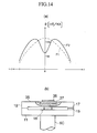
- Japanese Laid Open Application PS57-212719 discloses an electrode structure using the method (1).
- Fig. 14(a) shows a distribution of flux density of this electrode and
- Fig.14(b) shows the structure of the electrode.
- a coil electrode 11 is joined to an end of a movable conduction column 6C and a join port 15 is made therein and a spacer 18 is joined in the center area thereof.
- An electrode plate 12 is joined to the coil electrode 11 via the join port 15 and the spacer 18.
- a field adjust plate 36 of pure copper is buried in a surface 35 of the electrode plate 12 so as the reverse magnetic field to be produced by the eddy current generated by this field adjust plate 36.
- a contact element 37 is joined on the upper surface of the field adjust plate 36.
- dotted line F1 shows a distribution of flux density produced by an electrode having no such a field adjust plate like the plate 36.
- the maximum density of the flux comes to appear at the circumferential area by the reverse current generated by the field adjust plate 36, but the radial position of the maximum density is about 40% of the radius of the electrode and it is out of the scope of this invention.
- Japanese Patent Publication PH4-3611 shows an electrode which produces the similar distribution of flux density.
- Fig.15 shows the structure of the electrode and the characteristic of the distribution of flux density produced by the electrode.
- a coil 31 provided at an external place of an electrode 32 for producing a magnetic field
- the distribution of flux density of the electrode 32 becomes like a curved line G2 by an eddy current generated by a contact element 1B and the point of the maximum flux density appears at the circumference of the electrode 32.
- a dotted curve G1 shows a distribution characteristic of flux density produced solely by the coil 31.
- Japanese Laid Open Application PS57-20206 discloses an electrode structure using the method (2) set forth above.
- Fig.16 shows a characteristic of a distribution of flux density between electrodes using the method (2).
- the position giving the maximum flux density seems to fall in to the scope of this invention.
- the flux density produced by a coil for generating magnetic field at the center area of the electrode is reverse and the value at the center area of the electrode differs from that required by this invention.
- Japanese Patent Publication PH2-30132 discloses an electrode structure using the method (3).
- Fig.17 shows a distribution characteristic of flux density between electrodes using the method (3).
- the flux density at the center area of the electrode is not minus and the radial position giving the maximum flux density seems to fall in to the scope of this invention.
- the maximum value of flux density is about 2.5 times greater than that of given at the radial position 40% from the center of the electrode and this characteristic is out of the scope of this invention.
- an axial flux density distribution from the center to the circumference of the electrode is not monotonously increasing and at this point, it differs from this invention.
- One of the objects of this invention is to provide a vacuum valve which can raise the critical current that starts the arc concentration by means of unifying the flux density along the surface of the electrode.
- Another object of this invention is to provide a vacuum valve which improves the efficiency of current breaking by means of making the arc concentrate to plural points on the circumferential area of the electrode so as to decrease the current density at the area where the arc current is concentrating even if the current density on the surface of the electrode becomes higher than the critical current value and begins to concentrate.
- voltage drop Vcolm in an arc column relates to axial flux density Bz and current density Jz as expressed below.
- the voltage drop Vcolm tends to decrease even when a current of the same density flows.
- the degree of the voltage drop Vcolm between the electrodes is constant on the whole surface of the electrode and balances with the Vcolm on the circumferential area of the electrode, the current density Jz becomes high at the center area where the flux density is also high. This results in, in the conventional art, that the current density between the electrodes becomes high in the center area thereof as same as the flux density and it gradually decreases toward the circumference thereof as shown in Fig.12.
- this invention proposes to lower the axial flux density in the center area and to make the voltage drop large in the arc column at the center of the electrode so as to make the current flow uneasily.
- the vacuum arc is carried its current mainly by an electron flow and, in the region of flux density intensified, Lamor radius is small and the arc is effectively captured by the magnetic line of force.
- the current comes to steadily flow in the circumferential area of the electrode which producing strong magnetic field and it becomes possible to unify the current density between the electrodes compared to the conventional art.
- an invention claimed in claim 1 is a vacuum valve characterized by producing an axial magnetic field parallel to an arc generated between a movable and a stationary electrodes facing each other, and being adjusted a magnitude of an axial flux density between the electrodes as to increase gradually from a center area toward a circumferential area of each electrode, a point giving the maximum flux (Bp) density as to appear at a location equal to or outer than 70% of a radius from the center of each electrode, a flux density of a circumferential end of each electrode as to be equal to or greater than 2mT/KA and the maximum value (Bp) in a radial line from the center to the circumferential end as to be 1.4 to 2.4 times greater than a flux density (Bct) of the center of each electrode
- An invention claimed in claim 2 is a vacuum valve according to claim 1 characterized by the flux density (Bct) of the center of each electrode being adjusted as to be 0.75 to 0.9 times greater than a flux density (Bcr) which is produced when an arc voltage becomes the lowest according to a relationship between the arc voltage and the axial flux density, where the arc voltage is defined by the radius of each electrode and a breaking current.
- An invention claimed in claim 3 is a vacuum vale according to claim 2 characterized by a radial position producing the flux density (Bcr) according to the lowest arc voltage being adjusted as to locate within 20% to 40% area of the radius of each electrode.
- An invention claimed in claim 4 is a vacuum valve according to claims 1 to 3 characterized by proving plural portions on a circular line passing through a radial point on each electrode at which the maximum flux density (Bp) is to be produced, where flux densities are to be 0.6 to 0.9 times greater than the greatest value (Bmax) among the maximum flux densities (Bp).
- An invention claimed in claim 5 is a vacuum valve according to claim 4 characterized by a distribution of an axial flux density along the circular line passing through the radial point on each electrode at which the maximum flux density (Bp) is produced being adjusted as to have more than half portion of the circular line where, when the greatest value of flux density is set as Bmax and the smallest value of flux density as Bmin among the maximum flux densities (Bp), the flux density to be produced is greater than (Bmax+Bmin)/2.
- An invention claimed in claim 6 is a vacuum valve having a pair of electrodes each of which is accommodated in a vacuum chamber and joined to a conduction column for electrical connection with an external element and both of which are facing each other for contacting, and characterized by having a contact element on a surface of each electrode, the contact element having a graded characteristic that a degree of a cathode voltage drop continuously or gradually reduces from the center to the circumference thereof.
- An invention claimed in claim 7 is a vacuum valve according to claim 6 characterized by the contact element being made of copper-chrome (CuCr), and a weight percent of the chrome therein being adjusted to increase gradually from the center area to the outer side.
- CuCr copper-chrome
- An invention claimed in claim 8 is a vacuum valve having a pair of electrodes each of which is accommodated in a vacuum chamber and joined to a conduction column for electrical connection with an external element and both of which are facing each other for contacting, and characterized by having a plurality of magnetic field producing means at a position corresponding to a circumferential portion of each electrode.
- An invention claimed in claim 9 is a vacuum valve according to claim 8 characterized by each magnetic field generating means being made by a coil.
- An invention claimed in claim 10 is a vacuum valve according to claim 8 characterized by each magnetic field generating means being constructed by a conduction stud and a magnetic member arranged around the conduction stud.
- Fig.1 shows a distribution of an axial flux density between electrodes given along a radial direction of the electrodes of the first embodiment of this invention of a vacuum valve.
- the invention realizes the distribution of flux density that gives a low axial flux density Bct at the center of the electrode and increases gradually toward the circumference of the electrode, and it gives the maximum value Bp at the near point to the outer-most of the electrode by using a structure of electrode as shown in Fig.5
- Fig.2 shows a distribution characteristic of the axial flux density given along the circle passing the radial point of the vacuum valve of this invention, where the point gives the maximum value Bp.
- the distribution characteristic gives three concavities and convexities along the circle. The characteristic will be precisely explained after.
- this invention of a vacuum valve proposes to apply a flux density Bct at the center area of the electrode.
- the flux density Bct is adjusted within a range A of 0.75 to 0.9 times greater than the axial flux density Bcr (shown in Fig.3) which gives the lowest arc voltage between the electrodes against each breaking current.
- This invention also proposes to monotonously raise the axial flux density from the center to the circumferential area of the electrode.
- a radial position where the axial flux density Bcr which gives the lowest arc voltage Vmin is adjusted within a region B of 20% to 40% of the radius of the electrode.
- the axial flux density is made monotonously increase in an outer area from the region B and give the maximum value Bp in a circumferential area equal to or beyond 70% of the radius of the electrode.
- the maximum value Bp is adjusted within a range C of 1.4 to 2.4 times greater than the flux density Bct given at the electrode center.
- a circumferential distribution of flux density passing the radial position where the axial flux density gives the maximum value is made fluctuate high and low.
- the circumferential distribution of flux density is adjusted to give at least two peaks on the circle.
- the greatest value Bmax and the smallest value Bmin in the circumferential distribution of flux density are adjusted within a range of 1.4 to 2.4 times greater than the axial flux density Bct of the electrode center and also adjusted to have a region D equal to or broader than 50% of the circle where a flux density value shows equal to or greater than (Bmax+Bmin)/2.
- the axial flux density tends to increase from the center area toward the circumferential area of the electrode as shown in Fig.1, an arc generation in the circumferential area of the electrode becomes easier than the conventional electrode.
- the arc voltage does not rise so high even when the axial flux density becomes higher than the flux density Bcr which gives the lowest voltage Vmin, the arc to be generated can spread widely toward the circumferential end of the electrode.
- the breaking current increases, the arc voltage goes high in the region of high flux density as the relationship between the arc voltage and the flux density shown in Fig.3.
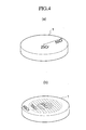
- copper-chrome (CuCr) material is used for the contact element 1, and the element 1 contains chrome of about 25wt% in the center area and about 50wt% in the most circumferential area, and the contamination rate of chrome is continuously raised from the center area toward the circumferential area in the contact element.
- Other usable material for the contact element is that of shown in Fig.4(b), wherein copper-chrome (CuCr) material is used for the contact element 1, and the element 1 contains chrome of about 25wt% in the center area, about 35wt% in the mid area and about 45wt% in the most circumferential area, that is the contamination rate of chrome is gradually raised by several steps from the center area toward the circumferential area in the contact element.
- each magnitude of the current density of the concentrated portions becomes relatively low because the arc does not concentrate to one point like the conventional structure but disperses to the several portions.
- the critical current value which starts the arc concentration is effectively raised.
- the portions of the arc concentration are to be in the circumferential area of the electrode, the area is broader than that in the center of the electrode and the damage caused by the arc energy is to be effectively reduced on the surface of the anode electrode.
- Fig.6 shows a model electrode of an embodiment of this invention. Breaking efficiency test was carried out between the model electrode, the conventional electrode of longitudinal magnetic field shown in Fig. 11 and a flat electrode shown in Fig.5.
- the flat electrode shown in Fig.5 is a simplified model of a contact element 1 with a conduction column 6, and an external coil 9 was used for producing a uniform magnetic field between the electrodes under the test.
- the different point of the model electrode for the vacuum valve of this invention shown in Fig.6 from the conventional one shown in Fig.11 is that a coil-shaped copper wire is used for a conducting path of current flow between a contact element and a conduction column in the former model.
- Other parts of the model are common to those of the conventional electrode shown in Fig.11.
- a collar 18a of a reinforcing element 18 is brazed to the upper end of a movable conduction column 6.
- a coil support ring 5 made of copper is engaged and brazed with the top of the reinforcing element 18 in a positioning hole 5a.
- a circular narrow groove is cut on the upper surface of support ring 5 and six circular spot-faces 5b are dug spacing 60® each other in the circumferential direction.
- a center coil 7 made of oxygen-free copper wire is mounted on the upper end of the reinforcing element 18 and brazed thereto.
- Each of six peripheral coils 3, which is the same with the center coil 7, is mounted in each spot-face 5b of the coil support ring 5 and brazed therein.
- a support cylinder 8 made of stainless steel is inserted at its bottom into the circular narrow groove cut around the positioning hole 5a of the coil support ring 5 and brazed therein.
- An electrode disk plate 2 is mounted on the tops of the support cylinder 8 and the peripheral coils 3.
- a through hole 2a is bored in the center of the electrode plate 2 and a circular narrow groove is cut as to face to the circular narrow groove of the coil support ring 5.
- the upper end of the support cylinder 8 is inserted into this circular narrow groove of the electrode plate 2 and brazed therein.
- Each spot-face 2b has the same diameter with spot-faces 5b and is located as to face to each spot-face 5b on the coil support ring 5.
- the top end of each peripheral coil 3 is brazed into each spot-face 2b.
- a projecting portion of a small base element 4 made of stainless steel is inserted into the through hole 2a in the center of the electrode plate 2 and brazed therein.
- the top end of the center coil 7 contacts to the lower surface of the small base element 4 and is brazed thereto.
- a diameter of a contact element 1 is the same with the diameter of the conventional contact element 1A shown in Fig.11. However, a shallow trapezoidal concave 1a is dug at the upper center of the contact element 1. The upper circumferential end of the contact element 1 is roundly chamfered.
- a vacuum valve constructed from this model electrode works as below. Referring to Fig. 6, most arc current generated between the contact element 1 of the movable electrode and the contact element of the stationary electrode flows from the contact element 1 through each peripheral coil 3 provided between the electrode plate 2 and the coil support ring 5, and the remnant of the arc current flows through the center coil 7.
- the current flowing through the center coil 7 is about one fourth of the total current flowing through the peripheral coils 3 since the resistance of the small base element affects to regulate the current flowing into the center coil 7.
- the stationary electrode is not shown in Fig.6, but it is arranged to face to the movable electrode so that the movable electrode comes to move back and forth against the stationary electrode.
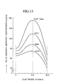
- Fig. 7 shows the result of breaking test.
- the test was carried out by using three kind of electrodes shown in Fig.5, Fig. 6 and Fig. 11.
- Fig. 7 shows the result of breaking test.
- the test was carried out by using three kind of electrodes shown in Fig.5, Fig. 6 and Fig. 11.
- this test by using the external coil 9 and superposing the uniform magnetic field produced by the external coil 9 over a magnetic field produced by each trial electrode so as to realize the best distribution of flux density since the distribution of flux density produced by each trial electrode is uncontrollable strictly by itself.
- the breaking characteristic D1 of the conventional longitudinal magnetic field electrode shown in Fig. 11 when the breaking characteristic D1 of the conventional longitudinal magnetic field electrode shown in Fig. 11 is set to 1, then the flat electrode shown in Fig.5 gives the maximum breaking limit D2 by 1.15 times higher than that of the conventional electrode under the condition that the external coil 9 produces the uniform magnetic field and the strength of the magnetic field produced by the external coil 9 is varied addequately.
- the model electrode of this invention shown in Fig.6 gives the maximum breaking limit D3 by 1.4 times higher than that of the conventional electrode and this apparently shows the breaking efficiency is to be improved by this model electrode.
- FIG. 8 A structure of an electrode shown in Fig.8 is also usable in a vacuum valve of this invention as well as that of shown Fig.6.
- the conduction studs 21 are placed circumferentially on the upper surface of the conduction column 6 and the outer portion of each conduction stud 21 is adjusted as to locate at the point of about 90% from the center in a radial direction of the electrode.
- Each magnetic member 22 is made as a right angle or an arc-shaped member with an angle of utmost 120° and is arranged around each conduction stud 21.
- this electrode of the structure By adoption of this electrode of the structure, moreover, it becomes possible to produce the axial magnetic field on the whole surface of the contact element 1 so as to effectively utilize the whole surface thereof. And the electrode shows efficient conductivity as the length of current path is shortened and the resistance between terminals is lowered.
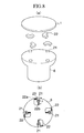
- Fig.9 shows the third embodiment of an electrode structure of this invention of a vacuum valve.
- plural conduction studs 24 with a small diameter are circumferentially arranged to be spaced each other between a contact element 1 and a conduction column 6.
- a magnetic member 25 having plural projections 25a from its disk body 25b is arranged on the top of the conduction column 6 so as each projection 25a to locate adjacent to each conduction stud 24.
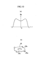
- a magnetic member 25 of a construction shown in Fig.10(b) of the fourth embodiment of this invention is usable as the substitute for the magnetic member 25 of the third embodiment shown in Fig.9.
- the magnetic member 25 shown in Fig. 10(b) is characterized by a disc body 25b having a center hole 25c which can improve the axial distribution Bz of flux density as shown in Fig.10(a). That is, the center hole 25c affects to lower the flux density of the center area of the electrode than that of the circumferential area thereof and to prevent the tendency of arc concentration to the center area of the electrode in breaking a large current, where the arc concentration tends to occur when the flux density is high in the center area.
- adoption of this magnetic member 25 of the construction shown in Fig.10(b) to the electrode accordingly, it becomes possible to broaden the arc over the whole surface of the contact element 1 even in breaking the large current near the critical limit and to improve the breaking efficiency.
- the relation between the number N of the conduction studs of small diameter and the diameter D (mm) of the electrode can be set as 0.05 D ⁇ N and as a result, it becomes possible to restrain the spatial fluctuation of flux and to let the arc break out uniformly over the surface of the contact element.
- each two conduction stud 21 or conduction stud 24 locating at both sides of each magnetic member 22 or each projection 25a of the magnetic member 25 by setting respective distances between the stud 21 and the magnetic member 22 or between the stud 24 and the projection 25a to differ each other, the flux produced around the conduction stud located at the nearer side by the current flowing therethrough tends to mainly pass through each magnetic member 22 or each projection 25a and, the affection from the flux of the reverse direction produced around the conduction stud located at the farther side by the current flowing therethrough is restrained. Therefore, the intensity of the magnetic pole appearing at each end of the magnetic member is strengthened and the high axial flux density is available.
- the contact element of graded characteristic where the material of the contact element is adjusted so as the cathode voltage drop to be continuously or gradually lowered from the center area to the circumferential area, the arc concentration to the center of the electrode is prevented and the distribution of current density in the arc is unified over the whole surface of the electrode and as a result, the critical current value of the arc concentration is improved and the breaking efficiency is raised.
Applications Claiming Priority (3)
| Application Number | Priority Date | Filing Date | Title |
|---|---|---|---|
| JP22643195 | 1995-09-04 | ||
| JP22643195 | 1995-09-04 | ||
| EP96929516A EP0790629B1 (de) | 1995-09-04 | 1996-09-04 | Vakuumschalter |
Related Parent Applications (1)
| Application Number | Title | Priority Date | Filing Date |
|---|---|---|---|
| EP96929516A Division EP0790629B1 (de) | 1995-09-04 | 1996-09-04 | Vakuumschalter |
Publications (3)
| Publication Number | Publication Date |
|---|---|
| EP1367619A2 true EP1367619A2 (de) | 2003-12-03 |
| EP1367619A3 EP1367619A3 (de) | 2003-12-10 |
| EP1367619B1 EP1367619B1 (de) | 2005-03-09 |
Family
ID=16845014
Family Applications (2)
| Application Number | Title | Priority Date | Filing Date |
|---|---|---|---|
| EP03017501A Expired - Lifetime EP1367619B1 (de) | 1995-09-04 | 1996-09-04 | Vakuumschalter |
| EP96929516A Expired - Lifetime EP0790629B1 (de) | 1995-09-04 | 1996-09-04 | Vakuumschalter |
Family Applications After (1)
| Application Number | Title | Priority Date | Filing Date |
|---|---|---|---|
| EP96929516A Expired - Lifetime EP0790629B1 (de) | 1995-09-04 | 1996-09-04 | Vakuumschalter |
Country Status (6)
| Country | Link |
|---|---|
| US (3) | US20020050485A1 (de) |
| EP (2) | EP1367619B1 (de) |
| KR (1) | KR100252839B1 (de) |
| CN (1) | CN1114220C (de) |
| DE (2) | DE69634458T2 (de) |
| WO (1) | WO1997009729A1 (de) |
Cited By (1)
| Publication number | Priority date | Publication date | Assignee | Title |
|---|---|---|---|---|
| FR2950729A1 (fr) * | 2009-09-29 | 2011-04-01 | Areva T & D Sas | Enroulement pour contact d'ampoule a vide a moyenne tension a coupure d'arc amelioree, ampoule a vide et disjoncteur, tel qu'un disjoncteur sectionneur d'alternateur associes |
Families Citing this family (13)
| Publication number | Priority date | Publication date | Assignee | Title |
|---|---|---|---|---|
| US6747233B1 (en) * | 2001-12-28 | 2004-06-08 | Abb Technology Ag | Non-linear magnetic field distribution in vacuum interrupter contacts |
| DE102005003812A1 (de) * | 2005-01-27 | 2006-10-05 | Abb Technology Ag | Verfahren zur Herstellung eines Kontaktstückes, sowie Kontaktstück für eine Vakuumschaltkammer selbst |
| CA2598440A1 (en) * | 2005-02-23 | 2006-08-31 | 3M Innovative Properties Company | Polymer blends |
| US7772515B2 (en) * | 2005-11-14 | 2010-08-10 | Cooper Technologies Company | Vacuum switchgear assembly and system |
| US7488916B2 (en) * | 2005-11-14 | 2009-02-10 | Cooper Technologies Company | Vacuum switchgear assembly, system and method |
| US8450630B2 (en) * | 2007-06-05 | 2013-05-28 | Cooper Technologies Company | Contact backing for a vacuum interrupter |
| US7781694B2 (en) * | 2007-06-05 | 2010-08-24 | Cooper Technologies Company | Vacuum fault interrupter |
| WO2011104751A1 (ja) * | 2010-02-24 | 2011-09-01 | 三菱電機株式会社 | 真空バルブ |
| KR101115639B1 (ko) * | 2010-10-18 | 2012-02-15 | 엘에스산전 주식회사 | 진공 인터럽터의 접점 어셈블리 |
| DE102011006899A1 (de) * | 2011-04-06 | 2012-10-11 | Tyco Electronics Amp Gmbh | Verfahren zur Herstellung von Kontaktelementen durch mechanisches Aufbringen von Materialschicht mit hoher Auflösung sowie Kontaktelement |
| US8653396B2 (en) * | 2011-09-28 | 2014-02-18 | Eaton Corporation | Vacuum switch and hybrid switch assembly therefor |
| EP2624273B1 (de) * | 2012-02-03 | 2015-04-01 | ABB Technology AG | Vakuumschaltröhre mit Übergangsbereichen zwischen Metallgehäuseteilen und Keramikgehäuseteilen, die mit Isoliermaterial bedeckt sind |
| US9777678B2 (en) * | 2015-02-02 | 2017-10-03 | Ford Global Technologies, Llc | Latchable valve and method for operation of the latchable valve |
Citations (4)
| Publication number | Priority date | Publication date | Assignee | Title |
|---|---|---|---|---|
| DE2242816A1 (de) * | 1971-09-06 | 1973-03-15 | Inst Prueffeld Elekt | Kontaktanordnung fuer vakuumschalter |
| DE3535066A1 (de) * | 1985-09-27 | 1986-02-27 | Ernst Prof. Dr.techn.habil. 1000 Berlin Slamecka | Erregerkontaktstueckanordnung fuer vakuumschalter |
| US4636600A (en) * | 1984-03-19 | 1987-01-13 | Holec Systemen Componenten B.V. | Vacuum switch provided with horseshoe-shaped elements for generating an axial magnetic field |
| JPH0757595A (ja) * | 1993-08-19 | 1995-03-03 | Toshiba Corp | 真空バルブ |
Family Cites Families (16)
| Publication number | Priority date | Publication date | Assignee | Title |
|---|---|---|---|---|
| US3622724A (en) * | 1970-02-24 | 1971-11-23 | Gen Electric | Vacuum-type circuit interrupter having contacts with improved arc-revolving means |
| GB1425641A (en) * | 1972-07-19 | 1976-02-18 | Siemens Ag | Vacuum switches |
| FR2242767B1 (de) * | 1973-08-30 | 1977-02-25 | Merlin Gerin | |
| JPS58810B2 (ja) * | 1976-12-06 | 1983-01-08 | 株式会社日立製作所 | 真空しや断器 |
| GB2050060B (en) * | 1979-05-22 | 1983-05-18 | Tokyo Shibaura Electric Co | Vacuum switches |
| JPS5772527U (de) * | 1980-10-21 | 1982-05-04 | ||
| JPS57212719A (en) * | 1981-06-24 | 1982-12-27 | Hitachi Ltd | Vacuum breaker |
| JPS58100325A (ja) * | 1981-12-09 | 1983-06-15 | 三菱電機株式会社 | 真空しや断器 |
| US4588879A (en) * | 1982-11-30 | 1986-05-13 | Kabushika Kaisha Meidensha | Vacuum interrupter |
| JPS59207523A (ja) * | 1983-05-09 | 1984-11-24 | 三菱電機株式会社 | 真空しや断器用電極 |
| JPS60220521A (ja) * | 1984-04-18 | 1985-11-05 | 株式会社東芝 | 真空バルブ |
| JPS6158124A (ja) * | 1984-08-30 | 1986-03-25 | 株式会社明電舎 | 真空インタラプタ |
| JPH01163938A (ja) * | 1987-12-21 | 1989-06-28 | Toshiba Corp | 真空バルブ |
| DE4002933A1 (de) * | 1990-02-01 | 1991-08-08 | Sachsenwerk Ag | Vakuumschaltkammer |
| JP3101329B2 (ja) * | 1991-01-10 | 2000-10-23 | 株式会社東芝 | 真空バルブ |
| KR100361390B1 (ko) * | 1994-11-16 | 2003-02-19 | 이턴 코포레이션 | 진공차단기,진공차단기용접점코일조립체및원주전극코일의제조방법 |
-
1996
- 1996-09-04 EP EP03017501A patent/EP1367619B1/de not_active Expired - Lifetime
- 1996-09-04 US US08/836,520 patent/US20020050485A1/en active Granted
- 1996-09-04 US US08/836,520 patent/US6376791B1/en not_active Expired - Fee Related
- 1996-09-04 DE DE69634458T patent/DE69634458T2/de not_active Expired - Lifetime
- 1996-09-04 WO PCT/JP1996/002498 patent/WO1997009729A1/ja active IP Right Grant
- 1996-09-04 DE DE69635605T patent/DE69635605T2/de not_active Expired - Lifetime
- 1996-09-04 KR KR1019970702935A patent/KR100252839B1/ko not_active IP Right Cessation
- 1996-09-04 CN CN96191162A patent/CN1114220C/zh not_active Expired - Fee Related
- 1996-09-04 EP EP96929516A patent/EP0790629B1/de not_active Expired - Lifetime
-
2001
- 2001-06-14 US US09/880,035 patent/US6426475B2/en not_active Expired - Fee Related
Patent Citations (4)
| Publication number | Priority date | Publication date | Assignee | Title |
|---|---|---|---|---|
| DE2242816A1 (de) * | 1971-09-06 | 1973-03-15 | Inst Prueffeld Elekt | Kontaktanordnung fuer vakuumschalter |
| US4636600A (en) * | 1984-03-19 | 1987-01-13 | Holec Systemen Componenten B.V. | Vacuum switch provided with horseshoe-shaped elements for generating an axial magnetic field |
| DE3535066A1 (de) * | 1985-09-27 | 1986-02-27 | Ernst Prof. Dr.techn.habil. 1000 Berlin Slamecka | Erregerkontaktstueckanordnung fuer vakuumschalter |
| JPH0757595A (ja) * | 1993-08-19 | 1995-03-03 | Toshiba Corp | 真空バルブ |
Cited By (3)
| Publication number | Priority date | Publication date | Assignee | Title |
|---|---|---|---|---|
| FR2950729A1 (fr) * | 2009-09-29 | 2011-04-01 | Areva T & D Sas | Enroulement pour contact d'ampoule a vide a moyenne tension a coupure d'arc amelioree, ampoule a vide et disjoncteur, tel qu'un disjoncteur sectionneur d'alternateur associes |
| WO2011039133A1 (fr) * | 2009-09-29 | 2011-04-07 | Areva T&D Sas | Enroulement pour contact d'ampoule à vide à moyenne tension à coupure d'arc ameliorée, ampoule à vide et disjoncteur, tel qu'un disjoncteur sectionneur d'alternateur associés |
| US8835790B2 (en) | 2009-09-29 | 2014-09-16 | Schneider Electric Energy France | Winding for a contact of a medium-voltage vacuum circuit-breaker with improved arc extinction, and an associated circuit-breaker and vacuum circuit-breaker, such as an AC generator disconnector circuit-breaker |
Also Published As
| Publication number | Publication date |
|---|---|
| EP0790629B1 (de) | 2005-12-21 |
| EP1367619B1 (de) | 2005-03-09 |
| US20010030174A1 (en) | 2001-10-18 |
| DE69635605D1 (de) | 2006-01-26 |
| CN1166232A (zh) | 1997-11-26 |
| US6376791B1 (en) | 2002-04-23 |
| EP0790629A4 (de) | 1999-06-09 |
| US20020050485A1 (en) | 2002-05-02 |
| WO1997009729A1 (fr) | 1997-03-13 |
| CN1114220C (zh) | 2003-07-09 |
| DE69635605T2 (de) | 2006-10-05 |
| KR100252839B1 (ko) | 2000-04-15 |
| DE69634458T2 (de) | 2006-01-05 |
| DE69634458D1 (de) | 2005-04-14 |
| EP1367619A3 (de) | 2003-12-10 |
| US6426475B2 (en) | 2002-07-30 |
| EP0790629A1 (de) | 1997-08-20 |
| KR970707564A (ko) | 1997-12-01 |
Similar Documents
| Publication | Publication Date | Title |
|---|---|---|
| EP0790629B1 (de) | Vakuumschalter | |
| US7173208B2 (en) | Vacuum interrupter | |
| JPH0322007B2 (de) | ||
| US20040050819A1 (en) | Contact for vacuum interrupter and vacuum interrupter using the contact | |
| JPS6171520A (ja) | 真空開閉器具の接触子装置 | |
| JPH0133013B2 (de) | ||
| JP2937881B2 (ja) | 真空バルブ | |
| KR101480845B1 (ko) | 진공 인터럽터 | |
| JPS58157017A (ja) | しや断器用真空バルブ | |
| US4855547A (en) | Vacuum interrupter | |
| JP3231595B2 (ja) | 真空バルブ | |
| SU1345271A1 (ru) | Контактна система вакуумной дугогасительной камеры | |
| WO2023276217A1 (ja) | 真空バルブ | |
| JP3243162B2 (ja) | 真空バルブ | |
| JPH11162302A (ja) | 真空バルブ | |
| JP3441224B2 (ja) | 真空バルブ及びその製造方法 | |
| JP2895449B2 (ja) | 真空バルブ | |
| JP2003092050A (ja) | 真空インタラプタ用接触子及び真空インタラプタ | |
| JP3219483B2 (ja) | 真空バルブ | |
| JPH01315914A (ja) | 真空バルブ | |
| JP2002270073A (ja) | 真空遮断器の電極 | |
| JPH06150784A (ja) | 真空バルブ | |
| JPH02270233A (ja) | 真空バルブ | |
| JPS6336916Y2 (de) | ||
| JP2003100184A (ja) | 真空インタラプタ用接触子及び真空インタラプタ |
Legal Events
| Date | Code | Title | Description |
|---|---|---|---|
| PUAI | Public reference made under article 153(3) epc to a published international application that has entered the european phase |
Free format text: ORIGINAL CODE: 0009012 |
|
| PUAL | Search report despatched |
Free format text: ORIGINAL CODE: 0009013 |
|
| 17P | Request for examination filed |
Effective date: 20030804 |
|
| AC | Divisional application: reference to earlier application |
Ref document number: 0790629 Country of ref document: EP Kind code of ref document: P |
|
| AK | Designated contracting states |
Kind code of ref document: A2 Designated state(s): DE FR |
|
| AK | Designated contracting states |
Kind code of ref document: A3 Designated state(s): DE FR |
|
| RIC1 | Information provided on ipc code assigned before grant |
Ipc: 7H 01H 33/18 B Ipc: 7H 01H 33/66 A |
|
| RIN1 | Information on inventor provided before grant (corrected) |
Inventor name: SOMEI, HIROMICHI Inventor name: HONMA, MITSUTAKA Inventor name: KANEKO, EIJI Inventor name: KAGENAGA, KIYOSHI Inventor name: WATANABE, KENJI Inventor name: SATO, JUNICHI Inventor name: UCHIYAMA, KUMI |
|
| 17Q | First examination report despatched |
Effective date: 20040225 |
|
| RIN1 | Information on inventor provided before grant (corrected) |
Inventor name: HONMA, MITSUTAKA Inventor name: KANEKO, EIJI Inventor name: SATO, JUNICHI Inventor name: KAGENAGA, KIYOSHI Inventor name: UCHIYAMA, KUMI Inventor name: SOMEI, HIROMICHI Inventor name: WATANABE, KENJI |
|
| AKX | Designation fees paid |
Designated state(s): DE FR |
|
| GRAP | Despatch of communication of intention to grant a patent |
Free format text: ORIGINAL CODE: EPIDOSNIGR1 |
|
| GRAS | Grant fee paid |
Free format text: ORIGINAL CODE: EPIDOSNIGR3 |
|
| GRAA | (expected) grant |
Free format text: ORIGINAL CODE: 0009210 |
|
| AC | Divisional application: reference to earlier application |
Ref document number: 0790629 Country of ref document: EP Kind code of ref document: P |
|
| AK | Designated contracting states |
Kind code of ref document: B1 Designated state(s): DE FR |
|
| REF | Corresponds to: |
Ref document number: 69634458 Country of ref document: DE Date of ref document: 20050414 Kind code of ref document: P |
|
| PLBE | No opposition filed within time limit |
Free format text: ORIGINAL CODE: 0009261 |
|
| STAA | Information on the status of an ep patent application or granted ep patent |
Free format text: STATUS: NO OPPOSITION FILED WITHIN TIME LIMIT |
|
| 26N | No opposition filed |
Effective date: 20051212 |
|
| ET | Fr: translation filed | ||
| PGFP | Annual fee paid to national office [announced via postgrant information from national office to epo] |
Ref country code: DE Payment date: 20130829 Year of fee payment: 18 |
|
| PGFP | Annual fee paid to national office [announced via postgrant information from national office to epo] |
Ref country code: FR Payment date: 20130910 Year of fee payment: 18 |
|
| REG | Reference to a national code |
Ref country code: DE Ref legal event code: R119 Ref document number: 69634458 Country of ref document: DE |
|
| REG | Reference to a national code |
Ref country code: DE Ref legal event code: R119 Ref document number: 69634458 Country of ref document: DE Effective date: 20150401 |
|
| REG | Reference to a national code |
Ref country code: FR Ref legal event code: ST Effective date: 20150529 |
|
| PG25 | Lapsed in a contracting state [announced via postgrant information from national office to epo] |
Ref country code: DE Free format text: LAPSE BECAUSE OF NON-PAYMENT OF DUE FEES Effective date: 20150401 |
|
| PG25 | Lapsed in a contracting state [announced via postgrant information from national office to epo] |
Ref country code: FR Free format text: LAPSE BECAUSE OF NON-PAYMENT OF DUE FEES Effective date: 20140930 |