EP1361511A1 - Data processing method and its apparatus - Google Patents
Data processing method and its apparatus Download PDFInfo
- Publication number
- EP1361511A1 EP1361511A1 EP02700588A EP02700588A EP1361511A1 EP 1361511 A1 EP1361511 A1 EP 1361511A1 EP 02700588 A EP02700588 A EP 02700588A EP 02700588 A EP02700588 A EP 02700588A EP 1361511 A1 EP1361511 A1 EP 1361511A1
- Authority
- EP
- European Patent Office
- Prior art keywords
- data
- circuit
- processing
- program
- set forth
- Prior art date
- Legal status (The legal status is an assumption and is not a legal conclusion. Google has not performed a legal analysis and makes no representation as to the accuracy of the status listed.)
- Ceased
Links
Images














































Classifications
-
- G—PHYSICS
- G06—COMPUTING OR CALCULATING; COUNTING
- G06F—ELECTRIC DIGITAL DATA PROCESSING
- G06F21/00—Security arrangements for protecting computers, components thereof, programs or data against unauthorised activity
- G06F21/30—Authentication, i.e. establishing the identity or authorisation of security principals
- G06F21/31—User authentication
- G06F21/34—User authentication involving the use of external additional devices, e.g. dongles or smart cards
-
- G—PHYSICS
- G06—COMPUTING OR CALCULATING; COUNTING
- G06F—ELECTRIC DIGITAL DATA PROCESSING
- G06F21/00—Security arrangements for protecting computers, components thereof, programs or data against unauthorised activity
- G06F21/50—Monitoring users, programs or devices to maintain the integrity of platforms, e.g. of processors, firmware or operating systems
- G06F21/52—Monitoring users, programs or devices to maintain the integrity of platforms, e.g. of processors, firmware or operating systems during program execution, e.g. stack integrity ; Preventing unwanted data erasure; Buffer overflow
- G06F21/53—Monitoring users, programs or devices to maintain the integrity of platforms, e.g. of processors, firmware or operating systems during program execution, e.g. stack integrity ; Preventing unwanted data erasure; Buffer overflow by executing in a restricted environment, e.g. sandbox or secure virtual machine
-
- G—PHYSICS
- G06—COMPUTING OR CALCULATING; COUNTING
- G06F—ELECTRIC DIGITAL DATA PROCESSING
- G06F9/00—Arrangements for program control, e.g. control units
- G06F9/06—Arrangements for program control, e.g. control units using stored programs, i.e. using an internal store of processing equipment to receive or retain programs
- G06F9/46—Multiprogramming arrangements
- G06F9/50—Allocation of resources, e.g. of the central processing unit [CPU]
- G06F9/5005—Allocation of resources, e.g. of the central processing unit [CPU] to service a request
- G06F9/5027—Allocation of resources, e.g. of the central processing unit [CPU] to service a request the resource being a machine, e.g. CPUs, Servers, Terminals
- G06F9/5038—Allocation of resources, e.g. of the central processing unit [CPU] to service a request the resource being a machine, e.g. CPUs, Servers, Terminals considering the execution order of a plurality of tasks, e.g. taking priority or time dependency constraints into consideration
-
- G—PHYSICS
- G06—COMPUTING OR CALCULATING; COUNTING
- G06Q—INFORMATION AND COMMUNICATION TECHNOLOGY [ICT] SPECIALLY ADAPTED FOR ADMINISTRATIVE, COMMERCIAL, FINANCIAL, MANAGERIAL OR SUPERVISORY PURPOSES; SYSTEMS OR METHODS SPECIALLY ADAPTED FOR ADMINISTRATIVE, COMMERCIAL, FINANCIAL, MANAGERIAL OR SUPERVISORY PURPOSES, NOT OTHERWISE PROVIDED FOR
- G06Q20/00—Payment architectures, schemes or protocols
- G06Q20/30—Payment architectures, schemes or protocols characterised by the use of specific devices or networks
- G06Q20/34—Payment architectures, schemes or protocols characterised by the use of specific devices or networks using cards, e.g. integrated circuit [IC] cards or magnetic cards
- G06Q20/341—Active cards, i.e. cards including their own processing means, e.g. including an IC or chip
-
- G—PHYSICS
- G07—CHECKING-DEVICES
- G07F—COIN-FREED OR LIKE APPARATUS
- G07F7/00—Mechanisms actuated by objects other than coins to free or to actuate vending, hiring, coin or paper currency dispensing or refunding apparatus
- G07F7/08—Mechanisms actuated by objects other than coins to free or to actuate vending, hiring, coin or paper currency dispensing or refunding apparatus by coded identity card or credit card or other personal identification means
- G07F7/0806—Details of the card
- G07F7/0813—Specific details related to card security
- G07F7/082—Features insuring the integrity of the data on or in the card
-
- G—PHYSICS
- G07—CHECKING-DEVICES
- G07F—COIN-FREED OR LIKE APPARATUS
- G07F7/00—Mechanisms actuated by objects other than coins to free or to actuate vending, hiring, coin or paper currency dispensing or refunding apparatus
- G07F7/08—Mechanisms actuated by objects other than coins to free or to actuate vending, hiring, coin or paper currency dispensing or refunding apparatus by coded identity card or credit card or other personal identification means
- G07F7/10—Mechanisms actuated by objects other than coins to free or to actuate vending, hiring, coin or paper currency dispensing or refunding apparatus by coded identity card or credit card or other personal identification means together with a coded signal, e.g. in the form of personal identification information, like personal identification number [PIN] or biometric data
- G07F7/1008—Active credit-cards provided with means to personalise their use, e.g. with PIN-introduction/comparison system
Definitions
- the present invention relates to a data processing method, its apparatus, its program, a semiconductor circuit, and an authentication apparatus useful in the case of conducting a transaction through a network using an IC (integrated circuit) built into a card or a mobile terminal apparatus.
- IC integrated circuit
- a server receives from for example reader/writers of IC cards or PCs (personal computers) processing requests using the IC cards and performs user authentication, data encryption and decryption, and other processing.
- the server has to be able to efficiently handle such processing requests.
- a server sometimes executes a plurality of application programs for processing for procedures relating to a plurality of settlement businesses and performs processing using selected application programs in accordance with the processing requests. Such processing requests also have to be efficiently handled.
- the application program executed by the server has to describe codes using key information for accessing IC cards and operational commands for operating the IC cards.
- the key information and operational commands can be known only by the manager of the server if expecting security of transactions using the IC cards.
- the manager of the server produced and customized the application programs upon request from the above service providers.
- application programs of a plurality of credit card companies or other businesses run.
- Such application programs are produced by the individual businesses and downloaded to the server using personal computers etc.
- the LSI forming the above explained server has a built-in CPU.
- the CPU sometimes accesses a memory outside of the LSI chip.
- the above explained server is sometimes comprised of a single computer.
- a single computer runs a plurality of programs relating to a plurality of services provided by different businesses.
- those services handle highly confidential data such as with settlements, there is the problem that there is a possibility of the highly confidential data owned by each business being illicitly acquired or tampered with by another business.
- FIG. 133 shows the basic configuration of a general computer 601.
- a CPU 602 performs processing using the instructions and data of a program read from a memory 603.
- the CPU 602 outputs an address for access in the memory 603 to an address bus 604.
- the CPU 602 reads from the memory 603 or writes in it according to a control signal S602.
- the module A, module B, and module C stored in the memory 603 are processing units of a program having specific functions.
- a debugger 605 checks the operation of the CPU 602 at the time of development of a program. It uses a HALT signal to temporarily halt the operation of the CPU 602, read internal information of the CPU 602, and inform that information to the program developer.
- the module A has a basic function used by the module B or the module C.
- the basic module (in this example, the module A) is stored in the memory 603 in advance and, rather than using it as a library, the developer develops the software assuming that the basic module is present at a specific location.
- the read content is in a machine language of a level which the CPU 602 executes, but there are tools for converting this machine language to an assembly language.
- the routine can be analyzed relatively easily.
- an application program running on the above explained server handles key data, charging data, log data, and other high security data set by the service provider, so there has been a demand for protecting it from illicit tampering or monitoring.
- a first object of the present invention is to provide a data processing method, semiconductor circuit, and program able to efficiently perform processing in accordance with a large number of processing requests.
- a second object of the present invention is to provide a data processing method, semiconductor circuit, and program enabling a user to produce and customize an application program of the user to be executed by a server without allowing the user to learn highly confidential information.
- a third object of the present invention is to provide a data processing method, semiconductor circuit, and program able to prevent each individual application program from being influenced by another application program when the same semiconductor circuit runs a plurality of application programs.
- a fourth object of the present invention is to provide a data processing method, semiconductor circuit, and program allowing transfer of data between application programs in accordance with need while preventing each application program from being illicitly tampered with, monitored, etc. by the user of another application program when the same semiconductor circuit runs a plurality of application programs.
- a fifth object of the present invention is to provide a data processing method, semiconductor circuit, authentication apparatus, and program enabling the content of access to a server or other semiconductor circuit to be restricted in accordance with rights to the same.
- a sixth object of the present invention is to provide a semiconductor circuit and data processing method enabling the confidentiality of data to be maintained even when transmitting highly confidential data between the semiconductor circuit and a semiconductor storage circuit through an external bus.
- a seventh object of the present invention is to provide a data processing apparatus enabling the confidentiality of instructions and data to be maintained between programs when executing a plurality of programs.
- An eighth object of the present invention is to provide a semiconductor circuit enabling the confidentiality of a program to be executed to be improved.
- a ninth object of the present invention is to provide a data processing apparatus, its method, and its program enabling the security of an application program running on the server to be improved when providing a service using an IC or other integrated circuit.
- the data processing method of the first aspect of the invention is a data processing method performed by a semiconductor circuit in accordance with a plurality of processing requests, comprising the steps of: generating job management data including job execution order data showing an order of execution of a plurality of jobs forming processing in accordance with a processing request and status data showing the state of progress of execution of the plurality of jobs for each of the plurality of processing requests, selecting one job management data from the generated plurality of job management data based on a predetermined rule, selecting a job to be executed next based on the status data and the processing order data of the selected job management data, executing the selected job, and updating the status data of the selected job management data in accordance with the execution of that job.
- the semiconductor circuit generates job management data including job execution order data showing an order of execution of a plurality of jobs forming processing in accordance with a processing request and status data showing the state of progress of execution of the plurality of jobs for each of the plurality of processing requests.
- the semiconductor circuit selects one job management data from the generated plurality of job management data based on a predetermined rule.
- the semiconductor circuit selects the job to be executed next based on the status data and the processing order data of the selected job management data.
- the semiconductor circuit executes the selected job.
- the semiconductor circuit updates the status data of the selected job management data in accordance with execution of that job.
- the data processing method of the first aspect of the invention preferably further comprises a step of updating the status data of the selected job management data, then selecting one job management data from the plurality of data modules.
- the data processing method of the first aspect of the invention preferably further comprises a step of selecting one job management data from the plurality of data modules after updating the status data of the selected job management data.
- the data processing method of the first aspect of the invention preferably further comprises a step of deleting the job management data when all jobs forming the processing in accordance with the processing request finish being executed.
- the data processing method of the first aspect of the invention preferably further comprises a step of receiving the processing requests from an integrated circuit having a storage unit storing data to be used for processing for a procedure performed with the semiconductor circuit or a communication apparatus inputting and outputting data with the integrated circuit.
- a semiconductor circuit of a second aspect of the invention is a semiconductor circuit for processing data in accordance with a plurality of processing requests, comprising an interface for inputting the plurality of processing requests, a storage circuit for storing job management data including job execution order data showing an order of execution of a plurality of jobs forming processing in accordance with a processing request and status data showing a state of progress of execution of the plurality of jobs, and a control circuit for generating the job management data for each of the input plurality of processing requests and storing it in the storage circuit, selecting one job management data from the generated plurality of job management data, selecting and executing the job to be executed next based on the status data and the processing order data of the selected job management data, and updating the status data of the selected job management data in accordance with the execution of that job.
- the interface inputs a plurality of processing requests.
- control circuit generates job management data including job execution order data showing an order of execution of a plurality of jobs forming processing in accordance with a processing request and status data showing a state of progress of execution of the plurality of jobs in accordance with the plurality of processing requests and stores them in the storage circuit.
- control circuit selects one job management data from the plurality of job management data.
- control circuit selects and executes the job to be executed next based on the status data and the processing order data of the selected job management data and updates the status data of the selected job management data in accordance with execution of that job.
- a program of a third aspect of the invention is a program to be executed by a semiconductor circuit for processing data in accordance with a plurality of processing requests, comprising a routine for generating job management data including job execution order data showing an order of execution of a plurality of jobs forming processing in accordance with a processing request and status data showing the state of progress of execution of the plurality of jobs for each of the plurality of processing requests, a routine for selecting one job management data from the generated plurality of job management data, a routine for selecting the job to be executed next based on the status data and the processing order data of the selected job management data, a routine for executing the selected job, and a routine for updating the status data of the selected job management data in accordance with the execution of the job.
- a data processing method of a fourth aspect of the invention is a data processing method performed by a semiconductor circuit running an application program for processing relating to a procedure using an integrated circuit, wherein the semiconductor circuit can view correspondence instructing data indicating correspondence between operation codes used for the application program to operate the integrated circuit and the names of the operations, that is, the operation names, having the semiconductor circuit receive as input an operation describing program describing the operations of the application program using the operation names, and having the semiconductor circuit obtain the operation codes corresponding to the operation names described in the operation describing program by viewing the correspondence instructing data and use the obtained operation codes to define the processing of the application program.
- the data processing method preferably further comprises having the correspondence instructing data further show the correspondence between the operation names and key information used when the integrated circuit performs operations corresponding to those operation names and having the semiconductor circuit obtain the key information corresponding to the operation names described in the operation describing program by viewing the correspondence instructing data and use that obtained key information to define the processing of the application program.
- the data processing method of the fourth aspect of the invention preferably further comprises having the semiconductor circuit generate job management data including job execution order data showing an order of execution of a plurality of jobs forming processing of the application program and status data showing the state of progress of execution of the plurality of jobs, select the job to be executed next based on the status data and the processing order data of the job management data, execute the selected job, and update the status data of the selected job management data in accordance with the execution of that job.
- a semiconductor circuit of a fifth aspect of the invention is a semiconductor circuit for running an application program for performing processing relating to a procedure using an integrated circuit, comprising a storage circuit for storing correspondence instructing data indicating correspondence between operation codes used for the application program to operate the integrated circuit and names of the operations, that is, operation names, an interface for inputting an operation describing program describing the operation of the application program using the operation names, and a control circuit for obtaining the operation codes corresponding to the operation names described in the input operation describing program by viewing the correspondence instructing data and using the obtained operation codes to define the processing of the application program.
- the interface inputs the operation describing program describing the operation of the application program using the operation names.
- control circuit obtains the operation codes corresponding to the operation names described in the input operation describing program by viewing the correspondence instructing data.
- control circuit uses the obtained operation codes to define the processing of the application program.
- a program of a sixth aspect of the invention is a program to be executed by a semiconductor circuit running an application program for performing processing relating to a procedure using an integrated circuit, comprising: a routine for inputting an operation describing program describing an operation of the application program using names of operations for the integrated circuit, that is, operation names, a routine for viewing correspondence instructing data indicating correspondence between operation codes used by the application program for operating the integrated circuit and the operation names to obtain the operation codes corresponding to the operation names described in the operation describing program, and a routine for using the obtained operation codes to define processing of the application program.
- a data processing method of a seventh aspect of the invention is a data processing method performed by a semiconductor circuit executing an application program, comprising the steps of: protecting each of a plurality of program modules forming the application program by a firewall allocated to the program module in advance in a plurality of firewalls, registering a program module linked with firewall identification information for identifying the firewall allocated to the program module, and executing the program module conditional on the registration being performed.
- the data processing method of the seventh aspect of the invention preferably further comprises a step of allowing data transfer or data viewing among a plurality of program modules registered linked with the same firewall identification information and prohibiting data transfer or data viewing among a plurality of program modules registered linked with different firewall identification information.
- the data processing method of the seventh aspect of the invention preferably further comprises the steps of: registering a program module further linked with download key information to be used when downloading the program module from the outside of the semiconductor circuit to the semiconductor circuit and, when receiving a download request for the program module, using the download key information registered linked with the program module to judge if download is possible and downloading the program module when judging that download is possible.
- a semiconductor circuit of an eighth aspect of the invention is a semiconductor circuit for running an application program, protecting each of a plurality of program modules forming the application program by a firewall allocated to each program module in advance in a plurality of firewalls, registering a program module linked with firewall identification information for identifying the firewall allocated to the program module, and executing the program module conditional on the registration being performed.
- a program of a ninth aspect of the invention is a program to be executed by a semiconductor circuit for executing an application program, comprising a routine for protecting each of a plurality of program modules forming the application program by a firewall allocated to each program module in advance in a plurality of firewalls, a routine for registering a program module linked with firewall identification information for identifying the firewall allocated to the program module, and a routine for executing the program module conditional on the registration being performed.
- a data processing method of a 10th aspect of the invention is a data processing method performed by a semiconductor circuit for executing an application program, comprising the steps of: independently executing a plurality of application programs protected by firewalls, registering in advance a condition for allowing communication between the application programs performed through the firewalls, judging if a communication request satisfies the registered condition when an application program generates a request for communication with another application program, and executing communication between the application programs in accordance with the communication request when judging that it satisfies the registered condition.
- a semiconductor circuit of an 11th aspect of the invention is a semiconductor circuit which independently executes a plurality of application programs protected by firewalls, registers in advance a condition for allowing communication between the application programs performed through the firewalls, judges if a communication request satisfies the registered condition when an application program generates a request for communication with another application program, and executes communication between the application programs in accordance with the communication request when judging that it satisfies the registered condition.
- the semiconductor circuit of the 11th aspect independently executes a plurality of application programs protected by firewalls.
- semiconductor circuit registers in advance a condition for allowing communication between the application programs performed through the firewalls.
- semiconductor circuit judges if a communication request satisfies the registered condition when an application program generates a request for communication with another application program.
- semiconductor circuit executes communication between the application programs in accordance with the communication request when judging that it satisfies the registered condition.
- a program of the 12th aspect of the invention is a program for making a semiconductor circuit execute a routine for independently executing a plurality of application programs protected by firewalls, a routine for registering in advance a condition for allowing communication between the application programs performed through the firewalls, a routine for judging if a communication request satisfies the registered condition when an application program generates a request for communication with another application program, and a routine for executing communication between the application programs in accordance with the communication request when judging that it satisfies the registered condition.
- a data processing method of a 13th aspect of the invention is a data processing method by which a semiconductor circuit or a semiconductor storage apparatus accessible by the semiconductor circuit downloads a program running in the semiconductor circuit, comprising the steps of: having the semiconductor circuit have a software structure comprised of a plurality of layers and having download signature verification key information corresponding to each layer able to be viewed by the semiconductor circuit, having the semiconductor circuit verify download signature information generated in accordance with a download request using the download signature verification key information when receiving the download request, and having the semiconductor apparatus allow the issuer of the download request to download a program of a layer corresponding to the download signature verification key information used for that verification conditional on the download signature information being legitimate.
- the data processing method of the 13th aspect of the invention further comprises a steps of: having an authentication apparatus store access master key information corresponding to a layer to which a program allowed to be downloaded belongs, having the authentication apparatus transmit the download request to the semiconductor circuit, and having the authentication apparatus use that access master key information to generate the download signature information and transmit that download signature information to the semiconductor circuit.
- the data processing method of the 13th aspect of the invention further comprises a steps of: having an authentication apparatus store identification information of the semiconductor circuit and having the authentication apparatus encrypt use the identification information as plain text using the access master key information to generate download master key information and use that download master key information to generate the download signature information.
- a semiconductor circuit of a 14th aspect of the invention is a semiconductor circuit having a software structure comprised of a plurality of layers, wherein the semiconductor circuit is able to view download signature verification key information corresponding to each layer, verifies download signature information generated in accordance with a download request using the download signature verification key information when receiving a download request, and allows the issuer of the download request to download a program of a layer corresponding to the download signature verification key information used for that verification to that semiconductor circuit or a semiconductor storage circuit accessible by the semiconductor circuit conditional on the download signature information being legitimate.
- the semiconductor circuit of the 14th aspect of the invention when receiving a download request, verifies the download signal information generated corresponding to that download request using download signature verification key information.
- semiconductor circuit allows the issuer of the download request to download a program of a layer corresponding the download signature verification key information used for that verification to that semiconductor circuit or a semiconductor storage circuit accessible by the semiconductor circuit conditional on the download signature information being legitimate.
- An authentication apparatus of a 15th aspect of the invention is an authentication apparatus used for authentication when downloading a program running in a semiconductor circuit to a semiconductor circuit having a software structure comprised of a plurality of layers or a semiconductor storage apparatus accessible by that semiconductor circuit, storing access master key information corresponding to a layer to which a program allowed to be downloaded belongs, transmitting the download request to the semiconductor circuit, and using that access master key information to generate the download signature information and transmitting that download signature information to the semiconductor circuit.
- the authentication apparatus of the 15th aspect of the invention first transmits the download request to the semiconductor circuit.
- the authentication apparatus uses access master key information to generate download signature information.
- the authentication apparatus transmits the download signature information to the semiconductor circuit.
- a program of a 16th aspect of the invention is a program to be executed by a semiconductor circuit having a software structure comprised of a plurality of layers, comprising a routine for verifying download signature information generated in accordance with a download request when receiving such a download request using the download signature verification key information of a corresponding layer in the plurality of layers, and a routine for allowing the issuer of the download request to download a program of a layer corresponding to the download signature verification key information used for that verification to that semiconductor circuit or a semiconductor storage circuit accessible by the semiconductor circuit conditional on the download signature information being legitimate.
- the semiconductor circuit of the 17th aspect of the invention inputs and outputs data with a bus outside of the semiconductor circuit through the data input/output processing circuit.
- the data input/output circuit encrypts the data input from the data processing circuit in units of predetermined data lengths and outputs the same to the bus.
- the data input/output circuit decrypts data input from the bus and outputs it to the data processing circuit.
- the data input/output circuit when accessing a semiconductor storage circuit based on a first address input from the data processing circuit, converts the first address to a second address so as to access the semiconductor storage circuit in units of storage areas in which the data of Nc is stored and uses that second address to access the semiconductor storage circuit.
- a data processing apparatus of a 19th aspect of the invention comprises a storage circuit for storing instructions and data of a plurality of programs, a computation circuit for accessing the storage circuit through a transmission line and using the instructions and data of the plurality of programs to execute the plurality of programs, a connection switching circuit interposed between the transmission line and the storage circuit for setting the transmission line and the storage circuit to one of a connection state and disconnection state based on a control signal, a connection control circuit for generating the control signal for control to set the transmission line and the storage circuit to one of a connection state and disconnection state based on access range defining data defining an address range in the storage circuit able to be accessed while the computation circuit is executing the plurality of programs for each of the plurality of programs, an address in the storage circuit for which the computation circuit issues an access request, and executing program instructing information which which program in a plurality of programs the computation circuit is executing, and an input/output interface circuit for inputting and outputting data with the computation circuit through the transmission line and inputting and
- connection control circuit preferably the connection control circuit generates the control signal indicating to set the transmission line and the storage circuit in a connection state when the address in the storage circuit for which the computation circuit issues an access request is inside the address range corresponding to a program being executed defined by the access range defining data and generates the control signal indicating to set the transmission line and the storage circuit in a disconnection state when it is not inside that address range.
- a semiconductor circuit of a 20th aspect of the invention is a semiconductor circuit for executing a program, comprising a first transmission line, a storage circuit for storing instructions or data for executing the program, a computation circuit for operating based on the instructions read through the first transmission line from the storage circuit, a first connection switching circuit for setting the first transmission line and the storage circuit in one of a connection state and disconnection state based on a first control signal, a second connection switching circuit for setting a second transmission line outside of that semiconductor circuit and the first transmission line in one of a connection state and disconnection state based on a second control signal, and a connection control circuit for outputting the second control signal instructing disconnection to the second connection switching circuit when outputting the first control signal instructing connection to the first connection switching circuit and outputting the second control signal instructing connection to the second connection switching circuit when outputting the first control signal instructing disconnection to the first connection switching circuit.
- the second connection switching circuit is connected through the second transmission line to a storage apparatus at the outside of the semiconductor circuit.
- the connection control circuit when the computation circuit reads instructions from the storage circuit, the connection control circuit outputs the first control signal instructing connection to the first connection switching circuit and outputs the second control signal instructing disconnection to the second connection switching circuit.
- a semiconductor circuit of a 21st aspect of the invention is a semiconductor circuit for executing a program, comprising an encryption/decryption circuit for storing encrypted instructions or data of the program, encrypting data to be output through a first transmission line outside of that semiconductor circuit to a storage apparatus, and decrypting encrypted instructions or data input through the first transmission line from the storage apparatus, a computation circuit for performing computation using the decrypted instructions or data, a selection circuit for selecting whether to allow communication between a second transmission line outside of the semiconductor circuit and the computation circuit based on a control signal, and a control circuit for outputting to the selection circuit the control signal for instructing to disallow communication between the second transmission line and the computation circuit while the computation circuit is performing processing using instructions or data of the program.
- a data processing apparatus of a 22nd aspect of the invention is a data processing apparatus comprising a storage circuit for storing in predetermined storage areas a plurality of application programs each comprised of a plurality of data modules including processing routine data describing processing routines for communicating with an integrated circuit to provide a service and storing management data showing linked together a data module, first key data used for using another data module in processing according to that data module, and second key data used for transferring data with the integrated circuit in processing according to that data module and a semiconductor circuit performing processing relating to a service based on a data modules, viewing the management data in that processing, using the first key data corresponding to that data module to use another data module, and using the second key data corresponding to that data module to transfer data with the integrated circuit.
- the storage circuit stores as a data module at least one of log data of processing performed performed using the data module, program data showing a routine for registering the data module in a storage area, program data showing a routine for deleting registration of the data module from the storage area, and program data showing a routine for defining the storage area for storing the application program.
- the semiconductor circuit uses the management data to obtain first key data corresponding to the predetermined data module and the first key data corresponding to the other data module and uses the other data module from the predetermined data module being executed conditional on the obtained two first key data matching.
- a data processing method of a 23rd aspect of the invention is a data processing method whereby a semiconductor circuit for communicating with an integrated circuit to perform processing to provide a service transfers data with a storage circuit, comprising the steps of: , when the storage circuit stores in predetermined storage areas a plurality of application programs each comprised of a plurality of data modules including processing routine data describing processing routines for communicating with an integrated circuit to providing a service and stores management data showing linked together a data module, first key data used for using another data module in processing in accordance with that data module, and second key data used for transferring data with the integrated circuit in processing according to that data module, having the semiconductor circuit perform processing relating to a service based on the data modules, having the semiconductor circuit view the management data in the processing relating to the service and use the first key data corresponding to a data module to use another data module, and having the semiconductor circuit use the second key data corresponding to the data module in processing relating to the service to transfer data with the integrated circuit.
- a program of a 24th aspect of the invention is a program to be executed by a semiconductor circuit for communicating with an integrated circuit to perform processing for providing services and transferring data with a storage circuit, comprising, when the storage circuit stores in predetermined storage areas a plurality of application programs each comprised of a plurality of data modules including processing routine data describing processing routines for communicating with an integrated circuit to provide services and stores management data showing linked together a data module, first key data used for using another the data module in processing according to that data module, and second key data used for transfer of data with the integrated circuit in processing according to that data module, a routine for performing processing relating to the service based on the data module, a routine for viewing the management data in processing relating to the service and using the first key data corresponding to that data module to use the other data module, and a routine for using the second key data corresponding to that data module in processing relating to the service to transfer data with the integrated circuit.
- a data processing apparatus able to maintain the confidentiality of instructions and data between programs when executing a plurality of programs.
- the present embodiment is an embodiment corresponding to the first to sixth aspects of the invention.
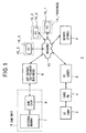
- FIG. 1 is a view of the overall configuration of a communication system 1 of the present embodiment.
- the communication system 1 uses a server 2 , IC card 3, card reader/writer 4 , personal computer 5, ASP (application service provider) server 6, and SAM (secure application module) unit 9 to communicate through the Internet 10 and perform settlement processing or processing for other procedures using the IC card 3 (integrated circuit of the present invention).
- server 2 IC card 3, card reader/writer 4 , personal computer 5, ASP (application service provider) server 6, and SAM (secure application module) unit 9 to communicate through the Internet 10 and perform settlement processing or processing for other procedures using the IC card 3 (integrated circuit of the present invention).
- ASP application service provider
- SAM secure application module
- the SAM unit 9 has an external memory 7 and a SAM chip (semiconductor circuit of the present invention) 8.
- the SAM chip 8 has the software configuration as shown in FIG. 2.
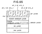
- the SAM chip 8 has, from a bottom layer toward a top layer, an HW (hardware) layer, OS layer, lower handler layer, higher handler layer, and AP layer.
- HW hardware
- the lower handler layer includes a driver layer.
- the AP layer includes application programs AP_1, AP_2, and AP_3 defining procedures for use of the IC card 3 by credit card companies or other businesses 15_1, 15_2, and 15_3 shown in FIG. 1.
- the application programs AP_1, AP_2, and AP_3 and the higher handler layer are provided between them with firewalls FW.
- the application program AP_1 is defined by a later explained service definition table data (correspondence instructing data) 20_1 and script program (operation describing program) 21_1 stored in an external memory 7.
- the application program AP_2 is defined by a later explained service definition table data (correspondence instructing data) 20_2 and script program (operation describing program) 21_2 stored in the external memory 7.
- the application program AP_3 is defined by a later explained service definition table data (correspondence instructing data) 20_3 and script program (operation describing program) 21_3 stored in the external memory 7.
- the SAM chip 8 is connected through a SCSI port, the Ethernet, etc. to the ASP server 6.
- the ASP server 6 is connected through the Internet 10 to a plurality of terminal apparatuses including a personal computer 5 of the end user and personal computers 16_1, 16_2, and 16_3 of the businesses 15_1, 15_2, and 15_3.
- the personal computer 5 for example, is connected through a serial port or USB port to a Dumb type card reader/writer 4.
- the card reader/writer 4 realizes for example wireless communication corresponding to the physical level with the IC card 3.
- Operational commands to the IC card 3 and response packets from the IC card 3 are generated and analyzed at the SAM unit 9 side. Therefore, the card reader/writer 4, personal computer 5, and ASP server 6 interposed between them only act to store the commands or response content in data payload portions and relay the same. They are not involved in encryption or decryption of data, authentication, and other actual operations in the IC card 3.
- the personal computers 16_1, 16_2, and 16_3 can download the later explained script program to the SAM chip 8 to customize their application programs AP_1, AP_2, and AP_3.
- FIG. 3 is a functional block diagram of an IC card 3.
- the IC card 3 has an IC (integrated circuit) 3a provided with a storage unit 50 and processing unit 51.
- the storage unit 50 has a storage area 55_1 used by a credit card company or other business 15_1, a storage area 55_2 used by a business 15_2, and a storage area 55_3 used by a business 15_3.
- the storage unit 50 stores key information used for judging the access right to the storage area 55_1, key information used for judging the access right to the storage area 55_2, and key information used for judging the access right to the storage area storage area 55_3. That key information is used for mutual authentication, encryption and decryption of data, etc.
- the storage unit 50 stores identification information of the IC card 3 or the user of the IC card 3.
- FIG. 5 is a view for explaining the data and programs stored in the external memory 7 shown in FIG. 1.
- the external memory 7 stores service definition table data 20_1 and IC card operation macro command script program 21_1 of the business 15_1.
- the external memory 7 stores service definition table data 20_2 and IC card operation macro command script program 21_2 of the business 15_2.
- the external memory 7 stores service definition table data 20_3 and IC card operation macro command script program 21_3 of the business 15_3.
- the service definition table data 20_1, 20_2, and 20_3 have the same format.
- IC card operation macro command script programs 21_1, 21_2, and 21_3 are written using common macro commands.
- service definition table data 20_1, 20_ 2, and 20_ 3 and IC card operation macro command script programs 21_1, 21_2, and 21_3 are scrambled to be stored in the external memory 7.
- the scrambled data and programs are descrambled at the SAM chip 8.
- script programs 21_1, 21_2, and 21_3 are produced using the personal computers 16_1, 16_2, and 16_3 shown in FIG. 1 by the businesses 15_1, 15_2, and 15 3 and are downloaded through the SAM chip 8 to the external memory 7.
- service definition table data 20_1, 20_2, and 20_3 are produced by the manager of the SAM unit 9 upon instruction from the businesses 15_1, 15_2, and 15_3.
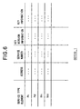
- FIG. 6 is a view for explaining the service definition table data 20_1.
- the service definition table data 20_1 has entries of service type elements (operation names) , addresses, service numbers (operation codes), key version information, and key information.
- the "service type element” shows the name assigned to the service provided by the application program of the business 15_1.
- the service type element is an identifier viewed instead of the service number of the service which the application program of the business 15_1 can use.
- the IC card operation macro command script program 21_1 define service content combining a plurality of service type elements and reflects this into the later explained IC card entity data (job management data) so as to be able to provide a service combining services corresponding to a plurality of service type elements.
- a service combining a service for reading data from the IC card 3 and a service for writing data in the server 2 can be defined in the IC card entity data.
- the service number in the service definition table data 20_1 is an operational command issued to the IC card 3 and analyzable by the IC card 3 when performing a service provided by the business 15_1.
- the "address" in the service definition table data 20_1 indicates the address at which data relating to a procedure relating to the corresponding service type element is stored.
- the "key version information" in the service definition table data 20_1 shows the version of the key information used when providing that service.
- the "key information" in the service definition table data 20_1 is the key information used when providing that service.
- key information used when accessing the storage area 55_1 of the IC 3a of the IC card 3 shown in FIG. 3 by the service definition table data 20_1 is set.
- the script program 21_1 is a program for defining the application program of the business 15_1 running on the SAM chip 8 and the procedure of processing performed by the IC card 3 when executing that application program.
- the SAM chip 8 uses the service definition table data 20_1 and script program 21_1 to generate IC card entity template data 30_1, an input data block 31_x1 output data block 32_x2, log data block 33_x3, and computation defining data block 34_x4 used for the procedure relating to the business 15_1.
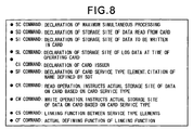
- FIG. 8 is a view for explaining the commands used for describing the IC card operation macro command script programs 21_1, 21_2, and 21_3.
- commands for the SAM chip 8 itself are given the first letter "S"
- commands relating to operation of the IC card 3 are given the first letter "C”.
- the second letter is selectively used in accordance with the application.
- I for an issuer setting declaration of the IC card 3, it is "I”
- S for a service type element declaration
- R for a simple read declaration from the IC card 3
- W for a simple write declaration to the IC card 3
- F for a service type element computation definition
- the commands used for describing the script programs 21_1, 21_2, and 21_3 include an SC command, SO command, SI command, SL command, SF command, CI command, CS command, CR command, and CW command.
- the SC command is a command declaring the number of the maximum number of IC card entity data which the SAM chip 8 can process simultaneously.
- the SO command is a command for declaring the data block for forming the output data block 32_x2 in which the data read from the IC card 3 is stored among the data blocks provided in the SAM chip 8 when performing processing using the IC card 3 based on the later explained IC card entity data.
- the SI command is a command for declaring the data block for forming the input data block 31_x1 in which the data to be written in the IC card 3 is stored among the data blocks provided in the SAM chip 8 when performing processing using the IC card 3 based on the later explained IC card entity data.
- the SL command is a command for declaring the data block forming the log data block 33_x3 for storing the log data relating to an operation among the data blocks provided in the SAM chip 8 when performing processing using the IC card 3 based on the later explained IC card entity data.
- the SF command is a command for providing the data block forming the computation defining data block 34_x4 describing the definition of the relation between the service type elements relating to the IC card 3.
- the content of the computation defining data block 34_x4 becomes the pre-processing information of the IC card entity data.
- the CI command is a command for declaring the issuer of the IC card 3 (business).
- the information specifying the business defined by the CI command becomes the IC card type information of the IC card entity data.
- the CS command is a command for declaring simultaneous operation of a plurality of services to the IC card 3 by citing service type elements.
- the CS command can also declare a function defining processing among service type elements.
- service type element designating information of the IC card entity data and processing order information are determined.
- the CR command declares to store data read from the IC card 3 in a designated data block when the relation among service type elements is not defined (when SF command is not described).
- the CW command declares to write data stored in a designated data block to the IC card 3 when the relation among service type elements is not defined.
- the CF command declares the data block describing computation content spanning services.
- This formula expresses the operation of subtracting 10 from the value of Wc when the remaining number of services Wc is larger than 10 and adding a number of points corresponding to 8% of Wc as cumulative points to Wd.
- FIG. 9 is a functional block diagram of the SAM chip 8 shown in FIG. 1.
- the SAM chip 8 has an ASPS communication interface unit 60, external memory communication interface unit 61, bus scramble unit 62, random number generation unit 63, encryption/decryption unit 64, storage unit 65, and CPU 66.
- the SAM chip 8 is a tamper-resistant module.
- the ASPS communication interface unit 60 is an interface used for input and output of data with the ASP server 6 shown in FIG. 1.
- the external memory communication interface unit 61 is an interface used for input and output of data with the external memory 7.
- the bus scramble unit 62 scrambles output data and descrambles input data when inputting and outputting data through the external memory communication interface unit 61.
- the random number generation unit 63 generates random numbers used at the time of authentication processing.
- the encryption/decryption unit 64 encrypts data and decrypts encrypted data.
- the storage unit 65 stores tasks, programs, and data used by the CPU 66.
- the CPU 66 executes a predetermined program (program of the present invention) to execute the later explained script download task, script interpretation task, entity generation task (job management data production task) and IC card procedure management task (job management data management task), and other tasks.
- a predetermined program program of the present invention
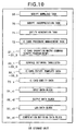
- FIG. 10 is a view for explaining the tasks, programs, and data stored in the storage unit 65.
- FIG. 10 it stores a script download task 69, script interpretation task 70, entity generation task 71, IC card procedure management task 72, IC card operation macro command script programs 21_1 to 21_3, service definition tables 20_1 to 20_3, IC card entity template data 30_1 to 30_3, IC card entity data 73_x, an input data block 31_x1, output data block 32_x2, log data block 33_x3, and computation defining data block 34_x4.
- the script download task 69 downloads the service definition table data 20_1 to 20_3 from, for example, the computers of businesses and loads them in the SAM chip 8.
- the script interpretation task 70 uses the service definition table data and script program to generate the IC card entity plate data, an input data block, output data block, log data block, and computation defining data block for each business.
- the number of data blocks generated for each business is not particularly limited.
- the entity generation task 71 When the entity generation task 71 receives from, for example, the ASP server 6 an entity production request, it conducts polling with the IC card 3, then generates the IC card entity data used for processing of a procedure between that IC card 3 and a business using the IC card entity plate data corresponding to that business. At this time, the IC card entity plate data becomes the class, and IC card entity data is generated as an instance of that class.
- the IC card procedure management task 72 uses the one or more IC card entity data 73_x present in the storage unit 65 to execute processing for a procedure between the IC card 3 and businesses 15_1 to 15_3.
- a plurality of processing for procedures performed between a plurality of IC cards 3 and the businesses 15_1 to 15_3 proceed simultaneously.
- the IC card procedure management task 72 executes the plurality of processing for procedures in parallel.
- the IC card procedure management task 72 deletes the IC card entity data 73_x when the series of procedures have been completed.
- the script programs 21_1 to 21_3 are input by the script download task 69 from, for example, the external memory 7 to the storage unit 65.
- the service definition table data 20_1 to 20 3 are input by the script download task 69 from, for example, the external memory 7 and stored in the storage unit 65.
- the IC card entity template data 30_1 to 30_3 are generated by the script interpretation task 70 and used as templates (classes) when generating the IC card entity data 73_x of the procedures relating to the respective businesses.
- the IC card entity data 73_x is generated by the entity generation task 71 using the IC card entity template data 30_1 to 30_3 as for example classes as an instance of the classes.
- the input data block 31_x1 output data block 32_x2, log data block 33_x3, and computation defining data block 34_x4 are generated by the script interpretation task 70.
- the IC card entity data 73_x is generated using IC card entity template data of a corresponding business already generated by entity generation task 71 in the SAM chip 8 when for example the SAM chip 8 receives a processing request for processing using the IC card 3 and the application program of a predetermined business from the ASP server 6.
- FIG. 11 is a view for explaining the format of the IC card entity data 73_x.
- the IC card entity data 73_x has management pointer information 80, entity ID information 81, entity status information (status data) 82, IC card type information 83, service type element designating information 84, processing order information (processing order data) 85, pre-processing information 86, and post-processing information 87.
- the management pointer information 80 is a bidirectional pointer for managing the IC card entity data 73_x in the storage unit 65.
- the entity ID information 81 is used for a request for generation of IC card entity data 73_x, confirmation of the state of progress, deletion, or the rest of a series of processing using the IC card entity data 73_x.
- the entity ID information 81 also becomes a return value given to the end user.
- the entity ID information 81 corresponds to the descriptor when opening a file in a general file system.
- the entity status information 82 shows the state of progress of a procedure relating to an IC card 3.
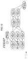
- the basic states of the IC card entity data 73_x include, as shown in FIG. 12, the state of processing for investigating the services which the IC card 3 can use (RS), the state of processing by which the SAM chip 8 authenticates the IC card 3 (A1), the state of processing by which the IC card 3 authenticates the SAM chip 8 (A2), the state of processing for reading data from the IC card 3 (R), and the state of processing for writing data in the IC card 3 (W).
- the processing for investigating the business, the processing for the SAM chip 8 to authenticate the IC card 3, the processing for the IC card 3 to authenticate the SAM chip 8, the processing for reading data from the IC card 3, and the processing for writing data in the IC card 3 correspond to jobs.
- a "job”, as explained later, is a unit of processing for which an order of execution is determined by the IC card procedure management task 72.
- A1 and A2 form the mutual authentication processing between the IC card 3 and SAM chip 8.
- the above-mentioned basic states are, as shown in the state transition chart of FIG. 12, managed divided into post-startup (after issuance of command) states and completed (after receiving response) states.
- the state of processing using the IC card entity data 73_x is managed by the instance generation (IC card entity data generation) state, RS post-startup state, RS completed state, A1 post-startup state, A1 completed state, A2 post-startup state, A2 completed state, R post-startup state, R completed state, W post-startup state, W completed state, and instance (IC card entity data) deletion state.
- instance generation IC card entity data generation
- the IC card type information 83 is information for specifying the business issuing that IC card 3.
- the IC card type information 83 is set with information defined by the CI command in the above-mentioned script program at the time of generation of the IC card entity data 73_x.
- the service type element designating information 84 shows the service type elements of the service defined in the service definition table data used in processing using the IC card entity data 73_x.
- the service type element designating information 84 is set with one or more service type elements designated by the CS command in the above-mentioned script program at the time of generation of the IC card entity data 73_x.
- the processing order information 85 shows the order of execution of services (jobs) used in the processing using the IC card entity data 73_x, that is, the state transition shown in FIG. 12.
- the processing order information 85 uses the service type elements to show the order of execution of jobs corresponding to the basic operations of the IC card 3.
- the jobs correspond to the RS, A1, A2, R, and W shown in FIG. 12.
- Specific operations on the IC card 3 are realized by the order of processing designated using the jobs.
- the processing order information 85 is set with "RS->R”.
- the processing order information 85 is set with "RS->A1->A2->R->W".
- the processing order information 85 is set with the order of jobs shown in FIG. 12 corresponding to the order of service elements designated in the CS command in the above-mentioned script program when generating the IC card entity data 73_x.
- the pre-processing information 86 is set from the ASP server 6 side with management data for performing processing using the IC card entity data 73_x.
- the pre-processing information 86 is set with points of a computation formula of a service designated in the SF data block.
- the pre-processing information 86 is set with the requested processing charge.
- the state relating to the amount of charge or number of points given etc. is set.
- the post-processing information 87 is set with data of the processing result of the IC card entity data 73_x required at the ASP server 6 side. For example, in the case of settlement, it is set with data showing the existence of a normal end to the settlement.
- the IC card procedure management task 72 is for example constantly being started up on the CPU 66 of the SAM chip 8 shown in FIG. 9.
- FIG. 13 is a flow chart of the processing performed by the IC card procedure management task 72.
- the IC card procedure management task 72 selects one IC card entity data 73_x for executing the next processing out of the plurality of IC card entity data 73_x present in the storage unit 65.
- the method of selection of that IC card entity data 73_x may be to successively select IC card entity data 73_x present in the storage unit 65 or to assign a priority order and select by priority in the order of the highest priority.
- the IC card procedure management task 72 judges if the job of the IC card entity data 73_x selected at step ST1 has already been started up. When judging that it has been started up, it proceeds to the processing of step ST5, while when judging that it has not been started up, proceeds to the processing of step ST3.
- the IC card procedure management task 72 judges from the entity status information 82 shown in FIG. 11 of the IC card entity data 73_x selected at step ST1 which state of the state transition chart shown in FIG. 12 the processing relating to that entity data is in and decides on the job to be executed next from the processing order information 85.
- the processing order information 85 defines the order of execution of jobs using the service elements set in the service definition table data as explained earlier.
- the IC card procedure management task 72 starts up the job selected at step ST3.
- the IC card procedure management task 72 executes the job using the data blocks relating to that job in the above-mentioned input data block 31_x1, output data block 32_x2, log data block 33_x3, and computation defining data block 34_x4.
- the IC card procedure management task 72 when issuing a command to the IC card 3 in execution of a job, uses the service element corresponding to that job as a key to search through the service definition table data to obtain the service number corresponding to that service element (operational command of IC card 3 able to be analyzed by the IC card 3) . Further, the IC card procedure management task 72 uses the obtained service number to issue a command to the IC card 3.
- the IC card procedure management task 72 when key information is required for accessing a storage area of the IC card 3a, uses the service element corresponding to that job to search through the service definition table data and obtain the key information corresponding to that service element. Further, the IC card procedure management task 72 uses that key information to perform mutual authentication with the IC card 3, encryption and decryption of data, and other processing and obtain the right to access a predetermined storage area of the IC card 3.
- Step ST5 is performed when the IC card procedure management task 72 issues a command to the IC card 3 and is waiting for the processing result of the IC card 3.
- the IC card procedure management task 72 When the IC card procedure management task 72 receives the processing result from the IC card 3, it sets this in the IC card entity data 73_x.
- the IC card procedure management task 72 updates the entity status information 82 of the IC card entity data 73_x shown in FIG. 11.
- the IC card procedure management task 72 performs processing for a plurality of IC cards 3 present in the SAM chip 8 in parallel while selecting in order the IC card entity data 73_x for the plurality of IC cards 3. Therefore, the SAM chip 8 can simultaneously proceed with the processing even when receiving processing requests for procedures using a plurality of IC cards 3.
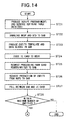
- FIG. 14 and FIG. 15 are views for explaining the overall operation of the communication system 1 shown in FIG. 1.
- the businesses 15_1 to 15_3 or a party requested by those businesses produce script programs 21_1, 21_2, and 21_3 describing processing for transactions performed by the businesses using the IC card 3 for example on the personal computers 16_1, 16_2, and 16_3 shown in FIG. 1.
- the manager of the SAM chip 8 produces service definition table data 20_1, 20_2, and 20_3 corresponding to the businesses 15_1 to 15_3.
- the service definition table data 20_1, 20_2, and 20_3 produced in step ST21 are stored in the external memory 7.
- script programs 21_1, 21_2, and 21_3 produced at step ST21 are downloaded from the personal computers 16_1, 16_2, and 16_3 through the Internet 10, ASP server 6, and SAM chip 8 to the external memory 7. That download processing is managed, as shown in FIG. 7, by the script download task 69 in the SAM chip 8.
- the script interpretation task 70 in the SAM chip shown in FIG. 7 uses the service definition table data and script program to generate the IC card entity plate data, input data block, output data block, log data block, and computation defining data block for each business.
- the generated data is stored in the storage unit 65 of the SAM chip 8 shown in FIG. 9.
- the user is issued the IC card 3.
- the storage unit 50 of the IC 3a of the IC card 3 stores key information used for transactions with the business the user contracts with.
- the server 2 issues a processing request through the Internet 10 to the ASP server 6.
- the ASP server 6 When the ASP server 6 receives a processing request from the server 2, it accesses the personal computer 5 through the Internet 10. Further, as shown in FIG. 16A, a processing request issued by the card reader/writer 4 for the IC card 3 is transmitted through the personal computer 5, Internet 10, and ASP server 6 to the SAM chip 8.
- the ASP server 6 outputs to the SAM chip 8 an entity production request.
- That entity production request stores information showing the issuer of the IC card 3.
- the SAM chip 8 When the SAM chip 8 receives an entity production request, as shown in FIG. 16B, it conducts polling with the IC card 3.
- the entity generation task 71 of the SAM chip 8 judges if the number of the IC card entity data 73_x present in the SAM chip 8 after the end of the polling is within the maximum number defined by the SC command of the script program. If within the maximum number, it proceeds to the processing of step ST29, while if not, it ends the processing.
- the entity generation task 71 specifies which business' IC card entity plate data to use based on the information showing the issuer of the IC card 3 stored in the entity production request for example and uses that specified IC card entity plate data to generate the IC card entity data 73_x.
- the SAM chip 8 outputs to the ASP server 6 the entity ID of the IC card entity data 73_x generated at step ST29.
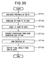
- the IC card procedure management task 72 of the SAM chip 8 investigates the services which the IC card 3 can use.
- the IC card procedure management task 72 of the SAM chip 8 authenticates the legitimacy of the IC card 3.
- the IC card 3 authenticates the legitimacy of the SAM chip 8.
- steps ST32 and ST33 the IC card 3 and SAM chip 8 mutually authenticate each other. This corresponds to FIG. 16C.
- the IC card procedure management task 72 of the SAM chip 8 reads and writes data necessary for the procedure with the IC card 3.
- the IC card procedure management task 72 uses a computation formula specified based on the pre-processing information 86 of the IC card entity data 73_x to perform predetermined processing for computation using the data read from the IC card 3.
- the IC card procedure management task 72 of the SAM chip 8 outputs the processing result of step ST34 to the ASP server 6.
- the IC card procedure management task 72 deletes the IC card entity data 73_x.
- the authentication system 1 since it is sufficient to store the IC card entity data 73_3 actually used for the processing of the IC cards 3 in the storage unit 65, it is possible to use the storage areas of the storage unit 65 efficiently.
- the IC card procedure management task 72 manages the states of execution of the jobs processed divided into post-startup states and completed states, it is possible to start the execution of one job, then start the processing relating to another job in the state while waiting for data from the IC card 3. Therefore, it is possible to eliminate the wait time caused by transfer of data with the IC card 3 through the Internet 10.
- the service definition table data describes a name showing the type of service provided by each business, that is, the service type element, the number of that service used in the IC card 3, and the key information used when providing that service. This is held in the external memory 7 . Therefore, businesses 15_1 to 15_3 not developers of the SAM chip 8 can produce their own application programs for running on the SAM chip 8 by the script programs 21_1, 21_2, and 21_3 and download them through the SAM chip 8 into the external memory 7 for customization. That is, without being informed of key information, operational commands for directly operating the IC card 3, or other highly confidential information to the businesses 15_1 to 15_3, these businesses can customize their own application programs. Further, when a business customizes its application program, it does not need to know the key information or card operational commands, so the load on the business is lightened.
- the authentication system 1 since it is possible to define computation content spanning a plurality of services, it is possible to provide diverse services combining a plurality of services in a range of services executed simultaneously with approval at the IC card 3 side.
- the authentication system 1 by introducing the concept of a data block, the data input and output with the IC card 3 and the log data can be easily managed.
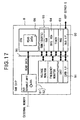
- FIG. 17 is a functional block diagram showing more specifically the function blocks of the SAM chip 8 shown in FIG. 9.
- the SAM chip 8 is connected through an internal bus 90 to an ASPS communication interface unit 60, external memory communication interface unit 61, bus scramble unit 62, random number generation unit 63, encryption/decryption unit 64, storage unit 65, and CPU 66.
- the present embodiment is an embodiment corresponding to the seventh to ninth aspects of the invention.
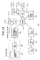
- FIG. 19 is a view of the overall configuration of a communication system 101 of the present embodiment.
- the communication system 101 uses the server 102 , IC card 103 (integrated circuit of the present invention), card reader/writer 104, personal computer 105, ASP (application service provider) server 106, SAM (secure application module) unit 109, personal computers 116_1, 116_2, and 116_3, and authentication units 117_1, 117_2, and 117_3 to communicate through the Internet 110 and perform settlement processing or other processing for a procedure using an IC card 103.
- IC card 103 integrated circuit of the present invention
- ASP application service provider
- SAM secure application module
- the SAM unit 109 has an external memory 107 (semiconductor storage circuit of the present invention) and SAM chip 108 (semiconductor circuit of the present invention).
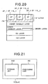
- the SAM chip 108 has the software configuration shown in FIG. 20.
- the SAM chip 108 has, from the bottom layer toward the top layer, an HW (hardware) layer, OS layer, lower handler layer, higher handler layer, and AP layer in that order.
- HW hardware
- the lower handler layer includes a driver layer.
- the AP layer has application programs AP_1, AP_2, and AP_3 defining procedures using the IC card 103 by the credit card companies or other businesses 115_1, 115_2, and 115_3 shown in FIG. 19.
- firewalls FW firewalls of the present invention
- the SAM chip 108 is connected through a SCSI port, the Ethernet, etc. to the ASP server 106.
- the ASP server 106 is connected through the Internet 110 to a plurality of terminal apparatus including a personal computer 105 of an end user and personal computers 116_1, 116_2, and 116_3 of businesses 115_1, 115_2, and 115_3.
- the personal computer 105 for example, is connected through a serial port or USB port to a Dumb type card reader/writer 104.
- the card reader/writer 104 realizes for example wireless communication corresponding to the physical level with the IC card 103.
- the operational commands to the IC card 103 and response packets from the IC card 103 are generated and analyzed at the SAM unit 109 side. Therefore, the card reader/writer 104, personal computer 105, and ASP server 106 between them only act to store the commands and response content in the data payload portion and relay the same and are not involved in the encryption or decryption of data, authentication, or other actual operations in the IC card 103.
- the businesses 115_1, 115_2, and 115_3 use their personal computers 116_1, 116_2, and 116_3 to produce the application programs AP_1, AP_2, and AP_3 and download the produced application programs through the authentication units 117_1, 117_2, and 117_3 through the SAM chip 108 to predetermined storage areas in the external memory 107.
- the storage areas in the external memory 107 where the application programs AP_1, AP_2, and AP_3 can be downloaded to are decided in advance and whether one has the right to download to such a storage area is verified by the SAM chip 108.
- firewalls FW restrict the transfer and viewing of data among the application programs AP_1, AP_2, and AP_3.
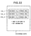
- FIG. 21 is a functional block diagram of the IC card 103.
- the IC card 103 has an IC (integrated circuit) 103a provided with a storage unit 150 and processing unit 151.
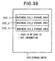
- the storage unit 150 has a storage area 155_1 used by a credit card company or other business 115_1, a storage area 155_2 used by a business 115_2, and a storage area 155_3 used by a business 115_3.
- the storage unit 150 stores key information used for judging the existence of the right to the storage area 155_1, key information used for judging the access right to the storage area 155_2, and key information used for judging the access right to the storage area 155_3. That key information is specifically used for mutual authentication, encryption and decryption of data, etc.
- the storage unit 150 stores identification information of the IC card 103 or IC card 103 user.
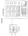
- FIG. 23 is a view for explaining the storage areas of the external memory 107.
- the storage areas of the external memory 107 include an AP storage area 120_1 storage area for storing the application program AP_1 of the business 115_1, an AP storage area 120_2 for storing the application program AP_2 of the business 115_2, an AP storage area 120_3 for storing the application program AP_3 of the business 115_3, an AP management storage area 121 used by the manager of the SAM chip 108, and a key information storage area 122.
- the application program AP_1 stored in the AP storage area 120_1 is comprised of a plurality of program modules. Access to the AP storage area 120_1 is restricted by the firewall FW_1.
- the application program AP_2 stored in the AP storage area 120_2 is comprised of a plurality of program modules. Access to the AP storage area 120_2 is restricted by the firewall FW_2.
- the application program AP_3 stored in the AP storage area 120_3 is comprised of a plurality of program modules. Access to the AP storage area 120_3 is restricted by the firewall FW_3.
- the above program module is the minimum unit downloaded for example from the outside of the SAM unit 109 to the external memory 107.
- the number of the program modules forming each application program can be freely determined by the corresponding business.
- the application programs AP_1, AP_2, and AP_3 stored in the external memory 107 are scrambled. They are descrambled when read into the SAM chip 108.
- the application programs AP_1, AP_2, and AP_3 are, for example, produced by the businesses 115_1, 115_2, and 115_3 using the personal computers 116_1, 116_2, and 116_3 shown in FIG. 19 and are downloaded through the SAM chip 108 to the external memory 107.
- Access to the AP management storage area 121 is restricted by the firewall FW_4.
- firewalls FW_1, FW_2, FW_3, and FW_4 correspond to the firewalls FW shown in FIG. 20.
- the AP management storage area 121 stores the module management data 130 shown in FIG. 24.
- the module management data 130 registers the module names of the program modules downloaded from the personal computers 116_1, 116_2, and 116_3 in advance and the download signature verification key information (download key information of the present invention).
- download of a program module is allowed conditional on the module management data 130 having the download signature verification key information registered in it in advance.
- module management data 130 has the module names of the program modules executed by the SAM chip 108 and the execution signature verification key information registered in it.
- the right for a program module to be executed by the SAM chip 108 is obtained conditional on the module management data 130 having the execution signature verification key information registered in it in advance.
- the module management data 130 shows the correspondence of the firewall number of the firewall restricting access to the program module (firewall identification information of the present invention), start address, address length, download signature verification key information, execution signature verification key information, and module name for each program module of the application programs AP_1, AP_2, and AP_3 stored in the AP storage areas 120_1, 120_2, and 120_3.
- the firewall number shows the number of the firewall by which access to that program module is restricted.
- the start address shows the start address of the storage area for which access is restricted by that firewall.
- the address length shows the address length of the storage area for which access is restricted by that firewall.
- the download signature verification key information is the key information used for the signature verification performed when downloading a program module through the SAM chip 108 to the external memory 107.
- the execution signature verification key information is used for verifying the signature information given to a program module when executing that program module by the SAM chip 108.
- each program module is given signature information showing its legitimacy.
- the execution signature verification key information it is possible to use the execution signature verification key information to verify that signature information to confirm the legitimacy of that program module.
- the module name is the name assigned to that program module.
- the key information storage area 122 stores the encrypted key information K_C1 used when accessing the storage area 155_1 of the IC card 103 shown in FIG. 22 by execution of the application program AP_1, the encrypted key information K_C2 used when accessing the storage area 155_2 of the IC card 103 shown in FIG. 22 by execution of the application program AP_2, and the encrypted key information K_C3 used when accessing the storage area 155_3 of the IC card 103 shown FIG. 22 by execution of the application program AP_3.
- the key information K_C1, K_C2, and K_C3 are encrypted by the key information K_X.
- Access to the key information storage area 122 is allowed only by the manager of the SAM chip 108.
- FIG. 25 is a functional block diagram of the SAM chip 108 shown in FIG. 19.
- the SAM chip 108 has an ASPS communication interface unit 160, external memory communication interface unit 161, bus scramble unit 162, signature processing unit 163, authentication processing unit 164, encryption/decryption unit 165, storage unit 166, and CPU 167.
- the SAM chip 108 is a tamper-resistant module.
- the ASPS communication interface unit 160 is an interface used for input and output of data with the ASP server 106 shown in FIG. 19.
- the external memory communication interface unit 161 is an interface used for input and output of data with the external memory 107.
- the bus scramble unit 162 scrambles output data and descrambles input data when inputting and outputting data through the external memory communication interface unit 161.
- the signature processing unit 163 as explained later produces a signature and verifies a signature when downloading an application program through the Internet 110 in the external memory 107 and when executing the application program.
- the authentication processing unit 164 as explained later performs mutual authentication with the other party when downloading an application program through the Internet 110 to the external memory 107.
- the encryption/decryption unit 165 encrypts data and decrypts encrypted data.
- the storage unit 166 for example stores the key information K_X for decrypting the key information K_C1, K_C2, and K_C3 stored in the key information storage area 122 of the above-mentioned external memory 107.
- the CPU 167 executes tasks as explained later based on a predetermined program (program of the present invention) and executes a designated application program in accordance with execution of the tasks.
- FIG. 26 is a view for explaining the tasks executed by the CPU 167.
- the CPU 167 executes the download task 170, system task 171, AP task 172 (program of the present invention), and settlement processing routine task 173.
- the download task 170 performs processing for downloading tan application program from outside of the SAM unit 109 through the SAM chip 108 to the external memory 107.
- the system task 171 is a task for performing driver management, operations unique to the IC card 103, and other processing.
- the AP task 172 comprehensively manages the execution of the application programs AP_1, AP_2, and AP_3 performed when the SAM chip 108 receives a processing request from the ASP server 106 or elsewhere outside of the SAM chip 108.
- the settlement processing routine task 173 decides which of the application programs AP_1, AP_2, and AP_3 to use when for example the SAM chip 108 receives a processing request relating to the IC card 103 from the ASP server 106.
- FIG. 27 is a flow chart for explaining the operation of downloading an application program AP_1 from the personal computer 116_1 shown in FIG. 19 to the external memory 107.
- the personal computer 116_1 shown in FIG. 19 transmits to the SAM chip 108 a download request designating the module name of each program module to be downloaded through the authentication unit 117_1.
- the download task 170 running on the SAM chip 108 shown in FIG. 26 performs mutual authentication with the authentication unit 117_1 connected to the personal computer 116_1. Further, when each others legitimacy is confirmed by the mutual authentication, the processing of step ST103 is performed.
- Both of the authentication unit 117_1 and SAM chip 108 hold identification information of the SAM chip 108, that is, the SAM_ID, and the mutual authentication master key information.
- the authentication unit 117_1 encrypts the SAM_ID by the mutual authentication master key information and transmits it to the SAM chip 108 .
- the SAM chip 108 decrypts the received encrypted SAM_ID by the mutual authentication master key and compares it with the SAM_ID it holds itself. If matching, it confirms the legitimacy of the authentication unit 117_1. Further, reverse to this, the SAM chip 108 encrypts the SAM_ID by the mutual authentication master key information and transmits it to the authentication unit 117_1.
- the authentication unit 117_1 decrypts the received encrypted SAM_ID by the mutual authentication master key and compares it with the SAM_ID it holds itself. If matching, it confirms the legitimacy of the SAM chip 108.
- the download task 170 judges whether each module name designated by the download request at step ST101 is registered in the module management data 130 stored in the AP management storage area 121 of the external memory 107.
- the download task 170 when judging at step ST103 that it is not registered, ends the processing without performing the download processing, while when judging that it is registered, performs the processing of step ST105.
- the authentication unit 117_1 encrypts the SAM_ID as plain text using the AP master key KEY-A to generate the download signature verification key information.
- the download task 170 when receiving the download signature verification key information at step ST105, judges if the received download signature verification key information matches with the download signature verification key information of the corresponding module name in the module management data 130.
- the download task 170 when receiving the signature information at step ST105, uses the download signature verification key information of the corresponding module name in the module management data 130 to judge the legitimacy of that signature information.
- the download task 170 proceeds to the processing of step ST108 when judging that they match at step ST106 or when judging that the signature information is legitimate and ends the processing in other cases.
- the download task 170 specifies the address in the external memory 107 corresponding to the module name designated at step ST101 by viewing the module management data 130 and downloads the program module from the personal computer 116_1 to the specified address on the external memory 107.
- FIG. 28 is a flow chart for explaining the operation by which the SAM chip 108 shown in FIG. 19 executes the application program AP_1.
- the SAM chip 108 When the SAM chip 108 receives a request for execution of the application program AP_1 for example from the ASP server 106, the AP task 172 shown in FIG. 26 executes the processing of step ST112.
- the AP task 172 Before the AP task 172 executes a program module of the application program AP_1, it can obtain execution signature verification key information corresponding to the module names of the program module by referring to the module management data 130.
- the AP task 172 uses the execution signature verification key information obtained at step ST112 to verify the legitimacy of the signal information of that program module.
- step ST113 When the AP task 172 verifies at step ST113 that the signature information is legitimate, it proceeds to the processing of step ST115, while when it judges it is not legitimate, it ends the processing.
- the AP task 172 executes the program module for which the signature information has been judged to be legitimate.
- program module may also be executed by the CPU 167 shown in FIG. 25 as a subroutine in the program.
- FIG. 29 is a view for explaining the operation for execution of an application program.
- the AP task 172 executes a code in a program module through the processing shown in FIG. 28, it judges whether the code to be executed next is a code instructing data transfer or data viewing with another program module.
- step ST124 When the AP task 172 judges that the code to be executed next does not instruct data transfer or data viewing with another program module, it proceeds to the processing of step ST124, while when it judges that it does instruct the same, proceeds to the processing of step ST123.
- the AP task 172 executes that code.
- the AP task 172 for example performs error processing without executing that code.
- FIG. 30 is a view for explaining the overall operation of the communication system 101 shown in FIG. 19.
- the businesses 115_1 to 115_3 or a party requested by these businesses produces the application programs AP_1, AP_2, and AP_3 for enabling the businesses to perform processing relating to transactions performed using the IC card 103 on the personal computers 116_1, 116_2, and 116_3 shown in FIG. 19.
- the manager of the SAM chip 108 generates the module management data 130 shown in FIG. 23, scrambles it, and stores it in the external memory 107.
- the application programs AP_1, AP_2, and AP_3 are downloaded through the authentication units 117_1, 117_2, and 117_3 from the personal computers 116_1, 116_2, and 116_3 to the SAM chip 108.
- the user is issued the IC card 103.
- the storage unit 150 of the IC 103a of the IC card 103 stores the key information used for transactions by the user with the contracting business.
- the user and a business may also conclude a contract through the Internet 110 etc. after issuance of the IC card 103.
- the server 102 sends a processing request through the Internet 110 to the ASP server 106.
- the ASP server 106 when receiving a processing request from the server 102, accesses the personal computer 105 through the Internet 110. Further, the processing request for the IC card 103 issued by the card reader/writer 104 is transmitted through the personal computer 105, Internet 110, and ASP server 106 to the SAM chip 108.
- the SAM chip 108 selects an application program by the settlement processing routine task 173 in accordance with the processing request received at step ST134 and executes that selected application program.
- the SAM chip 108 outputs the result of execution of the application program to the ASP server 106.
- the SAM chip 108 uses the authentication units 117_1, 117_2, and 117_3 to authenticate the downloader of the application program and allows the download of the application program only to an authorized storage area in the external memory 107, it is possible to prevent an unauthorized party from illicitly exchanging or tampering with an application program in the external memory 107.
- the SAM chip 108 runs a plurality of application programs, since data transfer and data and code viewing among application programs are restricted by the firewalls FW_1, FW_2, and FW_3, it is possible to prevent processing of each application program from being illicitly interfered with or tampered with by another application program. Further, it is possible to improve the confidentiality of each application program.
- the communication system 101 by comprising each application program by a plurality of program modules, it is possible to download to an external memory 107 in units of program modules.
- the communication system 101 by performing the usual scrambling on the highly confidential key information used for operations on an IC card 103 to encrypt it and storing it in the external memory 107, it is possible to improve the security level of that key information.
- the application program since the application program performs encryption and decryption at the time of code access by a bus scramble function, it is possible to prevent an application program stored in the external memory 107 from being illicitly analyzed etc. while halting the processing of the SAM chip 108.
- FIG. 31 is a functional block diagram showing more specifically the function blocks of the SAM chip 108 shown in FIG. 25.
- the SAM chip 108 is connected through an internal bus 190 to the ASPS communication interface unit 160, external memory communication interface unit 161, bus scramble unit 162, encryption/decryption unit 165, storage unit 166, and CPU 167.
- Part of the functions of the signature processing unit 163 and authentication processing unit 164 shown in FIG. 25 are realized by, for example, the CPU 167.
- the card I/F unit 191 connected to the internal bus 190 to an RF reception/transmission unit 192 outside of the SAM chip 108 and transfer data with the IC card 103 by a noncontact system through an antenna 192a of the RF reception/transmission unit 192.
- the present embodiment is an embodiment corresponding to the 10th to 12th aspects of the invention.
- FIG. 33 is a view of the overall configuration of a communication system 201 of the present embodiment.
- the communication system 201 uses a server 202, IC card 203, card reader/writer 204, personal computer 205, ASP (application service provider) server 206, SAM (secure application module) unit 209, personal computers 216_1, 216_2, and 216_3, and authentication units 217_1, 217_2, and 217_3 to communicate through the Internet 210 and perform settlement processing or other processing for a procedure using the IC card 203.
- server 202 IC card 203
- card reader/writer 204 personal computer
- personal computer 205 personal computer 205
- ASP application service provider
- SAM secure application module
- the SAM unit 209 has an external memory 207 and SAM chip 208.
- the SAM chip 208 has the software configuration shown in FIG. 34.
- the SAM chip 208 has, from the bottom layer toward the top layer, an HW (hardware) layer, OS layer, lower handler layer, higher handler layer, and AP layer in that order.
- HW hardware
- the lower handler layer includes a driver layer.
- AP layer includes application programs AP_1, AP_2, and AP_3 defining procedures using the IC card 203 by the credit card companies or other businesses 215_1, 215_2, and 215_3 shown in FIG. 33.
- the application programs AP_1, AP_2, and AP_3 and the higher handler layer are provided between them with firewalls FW.
- the SAM chip 208 is connected through a SCSI port, the Ethernet, etc. to the ASP server 206.
- the ASP server 206 is connected through the Internet 210 to a plurality of terminal apparatuses including the personal computer 205 of the end user and personal computers 216_1, 216_2, and 216_3 of the businesses 215_1, 215_2, and 215_3.
- the personal computer 205 for example, is connected through the serial port or USB port to a Dumb type card reader/writer 204.
- the card reader/writer 204 realizes for example wireless communication corresponding to the physical level with the IC card 203.
- the operational commands to the IC card 203 and the response packets from the IC card 203 are generated and analyzed at the SAM unit 209 side. Therefore, the card reader/writer 204, personal computer 205, and ASP server 206 interposed between them only act to store the commands or response contents in data payload portions and relay the same. They are not involved in the encryption or decryption of data, authentication, or other actual operations in the IC card 203.
- the businesses 215_1, 215_2, and 215_3 use the personal computers 216_1, 216_2, and 216_3 to produce the application programs AP_1, AP_2, and AP_3 and download the produced application programs through the authentication units 217_1, 217_2, and 217_3 and through the SAM chip 208 to predetermined storage areas in the external memory 207.
- the storage areas in the external memory 207 where the application programs AP_1, AP_ 2, and AP_3 can be downloaded are predetermined. Whether they have the right to download to those storage areas is verified by the SAM chip 208.
- FIG. 35 is a functional block diagram of the IC card 203.
- the IC card 203 has an IC (integrated circuit) 203a provided with a storage unit 250 and processing unit 251.
- the storage unit 250 has a storage area 255_1 used by a credit card company or other business 215_1, a storage area 255_2 used by a business 215_2, and a storage area 255_3 used by a business 215_3. Further, the storage unit 250 stores key information used for judging the existence of a right to the storage area 255_1, key information used for judging an access right to the storage area 255_2, and key information used for judging an access right to the storage area 255_3. That key information is specifically used for mutual authentication, encryption and decryption of data, etc.
- the storage unit 250 stores the identification information of the IC card 203 or the user of the IC card 203.
- FIG. 37 is a view for explaining the storage areas of the external memory 207.
- the storage areas of the external memory 207 include a storage area 220_1 in which the application program AP_1 of the business 215_1 is stored, a storage area 220_2 in which the application program AP_2 of the business 215_2 is stored, a storage area 220_3 in which the application program AP_3 of the business 215_3 is stored, and an AP management storage area 221 used by the manager of the SAM chip 208.
- the application program AP_1 stored in the AP storage area 220_1 is comprised of a plurality of program modules. Access to the AP storage area 220_1 is restricted by the firewall FW_1.
- the application program AP_2 stored in the AP storage area 220_2 is comprised of a plurality of program modules. Access to the AP storage area 220_2 is restricted by the firewall FW_2.
- the application program AP_3 stored in the AP storage area 220_3 is comprised of a plurality of program modules. Access to the AP storage area 220_3 is restricted by the firewall FW_3.
- the above program module is the minimum unit downloaded for example from the outside of the SAM unit 209 to the external memory 207.
- the number of the program modules forming each application program can be freely determined by the corresponding business.
- the application programs AP_1, AP_2, and AP_3 stored in the external memory 207 are scrambled. They are descrambled when read into the SAM chip 208.
- the application programs AP_1, AP_2, and AP_3 are, for example, produced by the businesses 215_1, 215_2, and 215_3 using the personal computers 216_1, 216_2, and 216_3 shown in FIG. 33 and are downloaded through the SAM chip 208 to the external memory 207.
- Access to the AP management storage area 221 is restricted by the firewall FW_4.
- firewalls FW_1, FW_2, FW_3, and FW_4 correspond to the firewalls FW shown in FIG. 34.
- the AP management storage area 221 stores the AP selection data 231 and the inter-AP communication data 232 as shown in FIG. 37.
- AP selection data 231 and inter-AP communication data 232 are, for example, registered in advance at the time of setting up the SAM chip 208. Further, the AP selection data 231 and inter-AP communication data 232 can only be rewritten by the manager of the SAM chip 208.
- FIG. 38 is a view for explaining the AP selection data 231.
- the AP selection data 231 shows the IC card type information and AP identification information linked together.
- the IC card type information shows the type of the IC card 203 shown in FIG. 33 and, for example, is identification information of the credit card company performing the settlement for a transaction using the IC card 203.
- the AP identification information is identification information of the application program operating at the AP layer of the SAM chip 208.
- FIG. 39 is a view for explaining the inter-AP communication data 232.
- the inter-AP communication data 232 shows whether communication among the application programs AP_1, AP_2, and AP_3 shown in FIG. 34 is possible
- this shows if the communication request to an application program at a row item issued by an application program at a column item shown in FIG. 39 is allowed or not.
- a communication request by the application program AP_3 to the application program AP_1 is allowed, but a communication request to the application program AP_2 is rejected.
- the AP management storage area 221 has an inter-AP communication storage area 233 used for communication (transfer of data) with an application program.
- FIG. 40 is a functional block diagram of the SAM chip 208 shown in FIG. 33.
- the SAM chip 208 has an ASPS communication interface unit 260, external memory communication interface unit 261, bus scramble unit 262, signature processing unit 263, authentication processing unit 264, encryption/decryption unit 265, storage unit 266, and CPU 267.
- the SAM chip 208 is a tamper-resistant module.
- the ASPS communication interface unit 260 is an interface used for input and output of data with the ASP server 206 shown in FIG. 33.
- the external memory communication interface unit 261 is an interface used for input and output of data with the external memory 207.
- the bus scramble unit 262 scrambles output data and descrambles input data when inputting and outputting data through the external memory communication interface unit 261.
- the external memory 207 stores data in a scrambled state.
- the signature processing unit 263 produces a signature and verifies a signature when downloading an application program through the Internet 210 to the external memory 207 and when executing an application program.
- the authentication processing unit 264 performs mutual authentication with the other party when downloading an application program through the Internet 210 to the external memory 207.
- the encryption/decryption unit 265 encrypts data and decrypts encrypted data.
- the storage unit 266 stores the data required for the processing of the CPU 267.
- the CPU 267 executes later explained tasks based on a predetermined program (program of the present invention) and executes an application program designated in accordance with execution of the tasks.
- FIG. 41 is a view for explaining tasks executed by the CPU 267.
- the CPU 267 executes a download task 270, system task 271, AP task 272, settlement processing routine task 273, inter-AP communication task 274, and inter-SAM communication task 275.
- the download task 270 performs processing for downloading an application program from outside of the SAM unit 209 through the SAM chip 208 to the external memory 207.
- the system task 271 is a task performing driver management, operations unique to the IC card 203, or other processing.
- the AP task 272 for example, comprehensively manages the execution of the application programs AP_1, AP_2, and AP_3 performed when a program request is received by the SAM chip 208 from the ASP server 206 or other place outside of the SAM chip 208.
- the settlement processing routine task 273 obtains identification information of the AP corresponding to the IC card type information included in that processing request based on the AP selection data 231 shown in FIG. 38 and selects and executes the application programs AP_1, AP_2, and AP_3 corresponding to that AP identification information.
- the inter-AP communication task 274 manages communication among the application programs.
- FIG. 43 is a flow chart for explaining the processing of the inter-AP communication task 274.
- step ST202 When an application program AP_1 being executed issues a communication request for writing data to AP_2, the processing of step ST202 is performed.
- the communication request issued at step ST201 is received by the inter-AP communication task 274.
- the inter-AP communication task 274 views the inter-AP communication data 232 shown in FIG. 39 and judges if the application program AP_1 can communicate with the AP_2.
- the inter-AP communication task 274 judges at step ST203 that communication is possible, it executes the processing of step ST205 while when it does not, it ends the processing.
- the application program AP_1 can communicate with the AP_2, so the processing of step ST205 is executed.
- the application program AP_1 Under the control of the inter-AP communication task 274, the application program AP_1 writes data in the inter-AP communication storage area 233 shown in FIG. 37.
- the inter-AP communication task 274 notifies the fact of the data being written to the application program AP_2.
- the application program AP_2 reads data from the inter-AP communication storage area 233 in accordance with the notification received at step ST206.
- the inter-SAM communication task 275 can for example start up the inter-SAM communication task 275 of an SAM chip 208x outside of the SAM chip 208 and issue a remote command to the inter-SAM communication task 275 of that SAM chip 208x.
- Such a remote command is issued by the inter-SAM communication task 275 of the SAM chip 208 to the inter-SAM communication task 275 of the SAM chip 208x to request that the SAM chip 208x execute at least part of the processing assigned to the SAM chip 208 when for example the processing load of the SAM chip 208 becomes large and it cannot suitably perform the processing.
- FIG. 45 is a view for explaining the overall operation of the communication system 201 shown in FIG. 33.
- the businesses 215_1 to 215_3 or a party requested by these businesses produce application programs AP_1, AP_2, and AP_3 for those businesses to perform processing for transactions using the IC card 203 on the personal computers 216_1, 216_2, and 216_3 shown in FIG. 33.
- the application programs AP_1, AP_2, and AP_3 are downloaded through the authentication units 217_1, 217_2, and 217_3 from the personal computers 216_1, 216_2, and 216_3 to the SAM chip 208.
- the user is issued the IC card 203.
- the IC 203a of the IC card 203 stores the key information used for transactions with a business which the user has contracted with.
- the server 202 issues a processing request through the Internet 210 to the ASP server 206.
- the ASP server 206 When the ASP server 206 receives a processing request from the server 202, it accesses the personal computer 205 through the Internet 210. Further, the processing request for the IC card 203 issued by the card reader/writer 204 is sent through the personal computer 205, Internet 210, and ASP server 206 to the SAM chip 208.
- the SAM chip 208 in accordance with the processing request received at step ST234, selects the application program by the settlement processing routine task 273 and executes the selected application program.
- any communication performed between application programs is performed by the inter-AP communication task 274 as shown in the above-mentioned FIG. 43.
- the SAM chip 208 outputs the results of execution of the application program to the ASP server 206.
- the application programs AP_1, AP_2, and AP_3 are restricted from accessing each other by firewalls, so it is possible to prevent application programs from being illicitly monitored and tampered with. Further, it is possible to improve the confidentiality of each application program.
- the settlement processing routine task 273 shown in FIG. 41 there is the automatic selection of application programs by the settlement processing routine task 273 shown in FIG. 41. That is, while the same level of computation content, for settlement processing differing in settlement protocol according to the issuer of the IC card 203, if the type of the IC card 203 is known, the corresponding application program can be automatically determined. Therefore, by registering the settlement processing at the level of the settlement processing routine task 273, the type of the IC card 203 and the corresponding application program can be automatically determined. Due to this, the load on the developer of the application program can be lightened.
- the communication system 201 since the information stored in the external memory 207 is scrambled by the bus scramble unit 262 of the SAM chip 208 shown in FIG. 40, there is confidentiality with respect to analysis from the outside.
- the communication system 201 by the provision of the inter-SAM communication task 275 shown in FIG. 41, it is possible to disperse the processing load of the SAM chip 208 to other SAM chips. Therefore, when mounting the SAM chip 208 in a store server etc. which has to simultaneously handle processing requests for settlement processing from a plurality of terminal apparatuses, it is possible to use the function of the inter-SAM communication task 275 to improve the settlement processing capability using a plurality of SAM chips 208.
- FIG. 46 is a functional block diagram showing more specifically the function blocks of the SAM chip 208 shown in FIG. 40.
- the SAM chip 208 is connected through an internal bus 290 to the ASPS communication interface unit 260, external memory communication interface unit 261, bus scramble unit 262, encryption/decryption unit 265, storage unit 266, and CPU 267.
- Part of the functions of the signature processing unit 263 and authentication processing unit 264 shown in FIG. 40 are for example realized by the CPU 267.
- the SAM chip 208 shown in FIG. 46 may also connect the card I/F unit 291 connected to the internal bus 290 to an RF reception/transmission unit 292 outside of the SAM chip 208 and transfer data with the IC card 203 by a noncontact system through an antenna 292a of the RF reception/transmission unit 292.
- This embodiment is an embodiment corresponding to the 13th to 16th aspects of the invention.
- FIG. 48 is a view of the overall configuration of the communication system 301 of the present embodiment.
- the communication system 301 uses the server 302, IC card 303 (integrated circuit of the present invention), card reader/writer 304, personal computer 305, ASP (application service provider) server 306, SAM (secure application module) unit 309, personal computers 316_1, 316_2, 316_3, 316_4, and 316_5, authentication units 317_1, 317_2, 317_3, 317_4, and 317_5 (authentication apparatuses of the present invention) , and the ICE (in-circuit emulator) 318 to communicate through the Internet 310 and develop or customize software of the SAM chip 308, perform settlement processing using the IC card 303, etc.
- server 302 IC card 303 (integrated circuit of the present invention), card reader/writer 304, personal computer 305, ASP (application service provider) server 306, SAM (secure application module) unit 309, personal computers 316_1, 316_2, 316_3, 316_4, and 316_5, authentication units 317_1, 317_2, 317_3, 317_4,
- the SAM unit 309 has an external memory 307 (semiconductor storage circuit of the present invention) and SAM chip 308 (semiconductor circuit of the present invention).
- the SAM chip 308 has a software configuration such as shown in FIG. 49.
- the SAM chip 308 has, from the lower layer to the upper layer, an HW (hardware) layer, OS layer, lower handler layer, higher handler layer, and application (AP) layer in that order.
- HW hardware
- OS OS layer
- AP application
- the lower handler layer is a layer defining the processing not dependent on the application program and corresponds to the transport layer, network layer, and data link layer in the OSI protocol.
- the lower handler layer includes a driver layer.
- the driver layer is a layer performing processing relating to the operation of the LSI.
- the higher handler layer is a layer defining the processing dependent on the application program and corresponds to a layer higher than the transport layer in OSI protocol.
- the OS layer corresponds to the first layer of the present invention
- the lower handler layer, driver layer, and higher handler layer correspond to the second layer of the present invention
- the AP layer corresponds to the third layer of the present invention.
- the AP layer includes the application programs AP_1, AP_2, and AP_3 defining the procedures for use of the IC card 303 by credit card companies and other businesses 315_AP1, 315_AP2, and 315_AP3 shown in FIG. 48.
- firewalls FW firewalls of the present invention
- the AP layer defines processing specific to each business, for example, the content of settlement processing using the IC card 303.
- the processing for directly operating the IC card 303 is defined by the layers of the higher handler layer on down.
- the SAM chip 308 is connected with the ASP server 306 through a SCSI port, the Ethernet, etc.
- the ASP server 306 is connected through the Internet 310 with the personal computers 305, 316_1, 316_2, 316_3, 316_4, and 316_5.
- the personal computer 316_1 is used by the business 315_AP1 of the application program AP_1 executed by the SAM chip 308.
- the personal computer 316_2 is used by the business 315_AP2 of the application program AP_1 executed by the SAM chip 308.
- the personal computer 316_3 is used by the business 315_AP3 of the application program AP_1 executed by the SAM chip 308.
- the personal computer 316_4 is used by the software developer 315_MID able to develop a higher handler layer and lower handler layer including the driver layer shown in FIG. 49 of the SAM chip 308.
- the personal computer 316_5 is used by the manufacturer of the SAM chip 308, that is, the software developer 315_SUP having the right to manage the SAM chips 308 as a whole.
- the businesses 315_AP1, 315_AP2, and 315_AP3 use the personal computers 316_1, 316_2, and 316_3 to produce the application programs AP_ 1, AP_2, and AP_3 and download the produced application programs through the authentication units 317_ 1, 317_ 2, and 317_3 to storage areas allocated in advance in the external memory 307 through the SAM chip 308.
- the businesses 315_AP1, 315_AP2, and 315_ AP3 are parties with no relation with each other, so the storage areas in the external memory 307 to which the application programs AP_1, AP_2, and AP_3 can be downloaded are determined in advance. Whether or not one has the right to download to such a storage area is verified by the SAM chip 308.
- firewalls FW restrict the transfer and viewing of data between the application programs AP_1, AP_2, and AP_3.
- the software developer 315 MID downloads a predetermined program into the SAM chip 308 through the authentication unit 317_4 in accordance with need to customize the higher handler layer and lower handler layer including the driver layer shown in FIG. 49 of the SAM chip 308 etc.
- the personal computer 305 for example, is used by the owner of the IC card 303, that is, the end user.
- the personal computer 305 for example, is connected through a serial port or USB port to a Dumb type card reader/writer 304.
- the card reader/writer 304 realizes for example wireless communication corresponding to the physical level with the IC card 303.
- the operational commands to the IC card 303 and the response packets from the IC card 303 are generated and analyzed at the SAM unit 309 side. Therefore, the card reader/writer 304, personal computer 305, and ASP server 306 interposed between them only act to store the commands or response contents in the data payload portions and relay the same. They are not involved in the encryption or decryption of data, authentication, or other operations in the IC card 303.
- ICE 318 is an emulator used when debugging a program running on the SAM chip 308.
- the IC card 303 stores the key information etc. necessary for the settlement processing using the SAM chip 308.
- FIG. 50 is a functional block diagram of the authentication unit 317_1.
- the authentication unit 317_1 has a storage unit 350_1 and processing unit 351_1.
- the storage unit 350_1 stores a SAM_ID, mutual authentication master key information K1, and access master key information KA.
- the SAM_ID is identification information of the SAM chip 308.
- the mutual authentication master key information K1 is, as explained later, used for generating mutual authentication key information K2.
- the access master key information KA is used for generating download signature information used when downloading a program in the external memory 307.
- the access master key information KA is key information necessary for downloading to the external memory 307 a program of the AP layer of the software structure of the SAM chip 308 shown in FIG. 49.
- the processing unit 351_1 has a mutual authentication unit 352_1 and download processing unit 353_1.
- the mutual authentication unit 352_1 when downloading a program to the external memory 307, encrypts the SAM_ID as plain text using the mutual authentication master key information K1 to generate the mutual authentication key information K2 and uses that mutual authentication key information K2 for mutual authentication with the SAM chip 308.
- the download processing unit 353_1 when downloading a program to the external memory 307, as shown in FIG. 52, encrypts the SAM_ID as plain text using the access master key information KA to generate the download key information K_DA. Further, the download processing unit 353_1 uses the download key information K_DA to generate the download signature information and transmits it to the SAM chip 308.
- the authentication units 317_2 and 317_3 are configured the same as the above explained authentication unit 317_1. However, for example, the content of the access master key information KA differs for each authentication unit.
- FIG. 53 is a functional block diagram of the authentication unit 317_4.
- the authentication unit 317_4 has a storage unit 350_4 and processing unit 351_4.
- the storage unit 350_4 stores a SAM_ID, mutual authentication master key information K1, and access master key information KA and KM.
- the SAM_ID, mutual authentication master key information K1, and access master key information KA are the same as those explained above.
- the access master key information KM is key information for downloading a program of the higher handler layer and the lower handler layer including the driver layer of the software structure of the SAM chip 308 shown in FIG. 49 to the external memory 307 or SAM chip 308.
- the processing unit 351_4 has a mutual authentication unit 352_4 and download processing unit 353_4.
- the mutual authentication unit 352_4 is the same as the mutual authentication unit 352_1 explained in FIG. 51.
- the download processing unit 353_4 when downloading a program to the external memory 307, as shown in FIG. 54, encrypts the SAM_ID as plain text using the access master key information KA to generate the download key information K_DA. Next, the download processing unit 353_4 encrypts the download key information K_DA as plain text using the access master key information KM to generate the download key information K_DM. Next, the download processing unit 353_4 uses the download key information K_DM to generate the download signature information and transmits it to the SAM chip 308.
- FIG. 55 is a functional block diagram of the authentication unit 317_5.
- the authentication unit 317_5 has a storage unit 350_5 and processing unit 351_5.
- the storage unit 350_5 stores a SAM_ID, mutual authentication master key information K1, and access master key information KA, KM, and KS.
- the SAM_ID, mutual authentication master key information K1, and access master key information KA and KM are the same as those explained above.
- the access master key information KS is the key information required for downloading a program of the OS layer of the software structure of the SAM chip 308 shown in FIG. 49 to the external memory 307 or SAM chip 308.
- the processing unit 351_5, as shown in FIG. 55, has a mutual authentication unit 352_5 and download processing unit 353_5.
- the mutual authentication unit 352_5 is the same as the mutual authentication unit 352_1 shown in the above-mentioned FIG. 51.
- the download processing unit 353_5 when downloading a program to the external memory 307, as shown in FIG. 56, encrypts the SAM_ID as plain text using the access master key information KA to generate the download key information K_DA.
- the download processing unit 353_5 encrypts the download key information K_DA as plain text using the access master key information KM to generate the download key information K_DM.
- the download processing unit 353_5 encrypts the download key information K_DM as plain text using the access master key information KS to generate the download key information K_DS.
- the download processing unit 353_5 uses the download key information K_DS to generate the download signature information and transmits this to the SAM chip 308.
- the authentication units 317_1, 317_4, and 317_5 store information in the storage units 350_1, 350_4, and 350_5 in a secure state. When these units are destroyed by outside factors or forced open, this is detected by a detection unit and the information stored in the storage units 350_1, 350_4, and 350_5 is deleted.
- FIG. 57 is a view for explaining the storage areas of the external memory 307.
- the storage areas of the external memory 307 include an AP storage area 320_1 in which the application program AP_1 of the business 315_1 is stored, an AP storage area 320_2 in which the application program AP_2 of the business 315_2 is stored, an AP storage area 320_3 in which the application program AP_3 of the business 315_3 is stored, and an AP management storage area 321 used by the manager of the SAM chip 308.
- the application program AP_1 stored in the AP storage area 320_1 is comprised of a plurality of program modules. Access to the AP storage area 320_1 is restricted by the firewall FW_1.
- the application program AP_2 stored in the AP storage area 320_2 is comprised of a plurality of program modules. Access to the AP storage area 320_2 is restricted by the firewall FW_2.
- the application program AP_3 stored in the AP storage area 320_3 is comprised of a plurality of program modules. Access to the AP storage area 120_3 is restricted by the firewall FW_3.
- the above program module is the minimum unit downloaded for example from the outside of the SAM unit 309 to the external memory 307.
- the number of the program modules forming each application program can be freely determined by the corresponding business.
- the application programs AP_1, AP_2 , and AP_3 stored in the external memory 307 are scrambled. They are descrambled when read into the SAM chip 308.
- the application programs AP_1, AP_2, and AP_3 are, for example, produced by the businesses 315_1, 315_2, and 315_3 using the personal computers 316_1, 316_2, and 316_3 shown in FIG. 48 and are downloaded through the SAM chip 308 to the external memory 307.
- Access to the AP management storage area 321 is restricted by the firewall FW_4.
- firewalls FW_1, FW_2, FW_3, and FW_4 correspond to the firewalls FW shown in FIG. 49.
- the AP management storage area 321 stores the AP management data 330.
- the AP management data 330 includes for example the SAM_ID, mutual authentication key information K2 (or mutual authentication master key information K1) and download signature verification key information K_DA, KDVM, and KDVS.
- the download signature verification key information K_DVA is key information for verifying the legitimacy of the signature information generated using the download key information K_DA.
- the download signature verification key information K_DVM is key information for verifying the legitimacy of the signature information generated using the download key information K_DM.
- the download signature verification key information K_DVS is key information for verifying the legitimacy of the signature information generated using the download key information K_DS.
- the download signature verification key information is key information used for signature verification performed when downloading that program module through the SAM chip 308 to the external memory 307.
- FIG. 58 is a functional block diagram of the SAM chip 308 shown in FIG. 48.
- the SAM chip 308 has an ASPS communication interface unit 360, external memory communication interface unit 361, bus scramble unit 362, encryption/decryption unit 363, storage unit 364, and CPU 365.
- the SAM chip 308 is a tamper-resistant module.
- the ASPS communication interface unit 360 is an interface used for input and output of data with the ASP server 306 shown in FIG. 48.
- the external memory communication interface unit 361 is an interface used for input and output of data with the external memory 307.
- the bus scramble unit 362 scrambles output data and descrambles input data when inputting and outputting data through the external memory communication interface unit 361.
- the encryption/decryption unit 363 encrypts data and decrypts encrypted data.
- the storage unit 364 stores data used for the processing by the CPU 365.
- the CPU 365 executes various processing including execution of an application program by the SAM chip 308 based on a predetermined program (program of the present invention) in the form of tasks etc.
- the CPU 365 for example, executes a download task 365a for performing processing for downloading program modules through the Internet 310.
- FIG. 59 is a flow chart for explaining that download operation.
- the personal computer 316_1 shown in FIG. 48 transmits a download request designating the module name of each program module to be downloaded comprising the application program AP_1 through the authentication unit 317_1, Internet 310, ASP server 306, and ICE 318 to the SAM chip 308.
- the mutual authentication unit 352_1 of the processing unit 351_1 of the authentication unit 317_1 performs mutual authentication with the download task 365a of the CPU 365 of the SAM chip 308 using the mutual authentication key information K2 generated at step ST302.
- step ST303 When the mutual legitimacy in the mutual authentication of step ST303 is confirmed, the unit proceeds to the processing of step ST305, while when not, it ends the processing.
- the download processing unit 353_1 uses the download key information K_DA generated at step ST305 to generate the download signature information.
- the download processing unit 353_1 transmits the download signature information generated at step ST306 to the SAM chip 308.
- the download task 365a of the CPU 365 of the SAM chip 308 shown in FIG. 58 uses the download signature verification key information K_DVA shown in FIG. 57 to judge the legitimacy of the download signature information received at step ST307 .
- the download task 365a judges if the download request has been made at the AP layer based on the module names received at step ST301 and specifies the download signature verification key information K_DVA.
- step ST308 If it is judged at step ST308 that the download signature information is legitimate, the task proceeds to the processing of step ST310, while if not, it ends the processing.
- the download task 365a of the CPU 365 of the SAM chip 308 shown in FIG. 58 specifies the address in the external memory 307 corresponding to a module name designated at step ST301 by viewing the module management data 330 and downloads the program module received from the personal computer 316_1 to that specified address on the external memory 307.
- the download key information K_ DM is generated by the routine explained using FIG. 54.
- the download signature information is generated.
- the download signature verification key information K_DVM shown in FIG. 57 is used to verify the download signature information.
- step ST305 when the software developer 315_SUP downloads a program module of the OS layer shown in FIG. 49 to the external memory 307, at step ST305, the routine explained using FIG. 56 is used to generate the download key information K_DS. Using this, at step ST306, the download signature information is generated. Further, at step ST308, in the SAM chip 308, the download signature verification key information K_DVS shown in FIG. 57 is used to verify the download signature information.
- the software developers 315_MID and 315_SUP can use the access master key information KA to download the program module of the AP layer to the external memory 307.
- the software developer 315_SUP can use the access master key information KA and KM to download program modules of the higher handler layer and lower handler layer to the external memory 307.
- FIG. 60 is a view for explaining the overall operation of the communication system 301 shown in FIG. 48.
- the businesses 315_1 to 315_3 or a part requested by these businesses produce application programs AP_1, AP_2, and AP_3 for those businesses to perform processing for transactions using the IC card 303 on the personal computers 316_1, 316_2, and 316_3 shown in FIG. 48.
- the application programs AP_1, AP_2, and AP_3 are downloaded through the authentication units 317 1, 317_2, and 317_3 from the personal computers 316_1, 316_2, and 316_3 to the SAM chip 308.
- the user is issued the IC card 303.
- the IC card 303 stores the key information used for transactions with a business which the user has contracted with.
- the server 302 issues a processing request through the Internet 310 to the ASP server 306.
- the ASP server 306 When the ASP server 306 receives a processing request from the server 302, it accesses the personal computer 305 through the Internet 310. Further, the processing request for the IC card 303 issued by the card reader/writer 304 is sent through the personal computer 305, Internet 310, and ASP server 306 to the SAM chip 308.
- the SAM chip 308 in accordance with the processing request received at step ST334, selects an application program by the settlement processing routine task and executes the selected application program.
- the SAM chip 308 outputs the result of execution of the application program to the ASP server 306.
- the authentication units 317_1, 317_4, and 317_5 store information in a secure state in the storage units 350_1, 350_4, and 350_5.
- a detection unit When such a unit is destroyed by an external factor or forced open, this is detected by a detection unit and the stored information in the storage units 350_1, 350_4, and 350_5 is deleted. Therefore, illicit use of the key information used for downloading to the SAM chip 308 can be avoided.
- the SAM chip 308 when the SAM chip 308 operates a plurality of application programs, since data transfer or viewing of data and codes between application programs is restricted by the firewalls FW_1, FW_2, and FW_3, illicit interference or tampering with the processing of each application program by another application program can be prevented. Further, it is possible to enhance the secrecy of each application program.
- each application program by configuring each application program by a plurality of program modules, it is possible to download to the external memory 307 in program modules units.
- the communication system 301 by encrypting the highly confidential key information used for operation of the IC card 303 in addition to the usual scrambling and storing it in the external memory 307, it is possible to improve the security level of the key information.
- the application program can execute encryption and decryption when accessing codes by the bus scramble function, so it is possible to prevent an application program stored in the external memory 307 from being illicitly analyzed etc. while processing of the SAM chip 308 is halted.
- FIG. 61 is a functional block diagram showing more specifically the function blocks of the SAM chip 308 shown in FIG. 58.
- the SAM chip 308 is connected through an internal bus 390 to the ASPS communication interface unit 360, external memory communication interface unit 361, bus scramble unit 362, encryption/decryption unit 365, storage unit 364, and CPU 366.
- the card I/F unit 391 connected to the internal bus 390 to an RF reception/transmission unit 392 outside of the SAM chip 308 and transfer data with the IF card 303 by a noncontact system through an antenna 392a of the RF reception/transmission unit 392.
- the present invention is not limited to the above explained embodiment.
- the case of providing the authentication units 317_1 to 317_5 for the Internet 310 at the personal computer 316_1 to 316_6 side was illustrated, but as shown in FIG. 63, it is also possible to provide the authentication units 317_1 to 317_5 in the SAM chip 308 and allow access to the authentication units 317_1 to 317_5 to the corresponding personal computers 316_1 to 316_5.
- the present embodiment is an embodiment corresponding to the 17th and 18th aspects of the invention.
- FIG. 64 is a view of the overall configuration of the communication system 401 of the present embodiment.
- the communication system 401 uses the server 402, IC card 403, card reader/writer 404, personal computer 405, ASP (application service provider) server 406, SAM (secure application module) unit 409, personal computers 416_1, 416_2, and 416_3, and authentication units 417_1, 417_2, and 417_3 to communicate through the Internet 410 and perform settlement processing or other processing for a procedure using the IC card 403.
- server 402 IC card 403, card reader/writer 404
- personal computer 405 personal computer 405
- ASP application service provider
- SAM secure application module
- the SAM unit 409 has an external memory 407 and SAM chip 408.
- the SAM chip 408 has a software configuration shown in FIG. 65. As shown in FIG. 65, the SAM chip 408 has, from a bottom layer toward a top layer, an HW (hardware) layer, OS layer, lower handler layer, higher handler layer, and AP layer.
- HW hardware
- the lower handler layer includes a driver layer.
- the AP layer includes application programs AP_1, AP_2, and AP_3 defining procedures for use of the IC card 403 by credit card companies or other businesses 415_1, 415_2, and 415_3 shown in FIG. 64.
- the application programs AP_1, AP_2, and AP_3 and the higher handler layer are provided between them with firewalls FW.
- the SAM chip 408 is connected through a bus 419 using a SCSI port, the Ethernet, etc. to the ASP server 406.
- the ASP server 406 is connected through the Internet 410 to a plurality of terminal apparatuses including a personal computer 405 of the end user and personal computers 416_1, 416_2, and 416_3 of the businesses 415_1, 415_2, and 415_3.
- the personal computer 405 is connected through a serial port or USB port to a Dumb type card reader/writer 404.
- the card reader/writer 404 realizes for example wireless communication corresponding to the physical level with the IC card 403.
- Operational commands to the IC card 403 and response packets from the IC card 403 are generated and analyzed at the SAM unit 409 side. Therefore, the card reader/writer 404, personal computer 405, and ASP server 406 interposed between them only act to store the commands or response content in data payload portions and relay the same. They are not involved in encryption or decryption of data, authentication, and other actual operations in the IC card 403.
- the businesses 415_1, 415_2, and 415_3 use the personal computers 416_ 1, 416_2, and 416_3 to produce the application programs AP_1, AP_2, and AP_3 and download the produced application programs through the authentication units 417_1, 417_2, and 417_3 through the SAM chip 408 to preassigned storage areas in the external memory 407.
- the storage areas in the external memory 407 where the application programs AP_1, AP_2 , and AP_3 can be downloaded are decided in advance and whether one has the right to download to such a storage area is verified by the SAM chip 408.
- FIG. 66 is a view for explaining the storage areas of the external memory 407.
- the storage areas of the external memory 407 include an AP storage area 420_1 for storing the application program AP_1 of the business 415_1, an AP storage area 420_2 for storing the application program AP_2 of the business 415_2, an AP storage area 420_3 for storing the application program AP_3 of the business 415_3, and an AP management storage area 421 used by the manager of the SAM chip 408.
- the application program AP_1 stored in the AP storage area 420_1 is comprised of a plurality of program modules. Access to the AP storage area 420_1 is restricted by the firewall FW_1.
- the application program AP_2 stored in the AP storage area 420_2 is comprised of a plurality of program modules. Access to the AP storage area 420_2 is restricted by the firewall FW_2.
- the application program AP_3 stored in the AP storage area 420_3 is comprised of a plurality of program modules. Access to the AP storage area 420_3 is restricted by the firewall FW_3.
- the above program module is the minimum unit downloaded for example from the outside of the SAM unit 409 to the external memory 407.
- the number of the program modules forming each application program can be freely determined by the corresponding business.
- the application programs AP_1, AP_2, and AP_3 are, for example, produced by the businesses 415_1, 415_2, and 415_3 using the personal computers 416_1, 416_2, and 416_3 shown in FIG. 64 and are downloaded through the SAM chip 408 to the external memory 407.
- Access to the AP management storage area 421a is allowed only by the manager of the SAM chip 408 by the firewall FW_4.
- firewalls FW_1, FW_2, FW_3, and FW_4 correspond to the firewalls FW shown in FIG. 65.
- the AP management storage area 421 stores the module management data 421 shown in FIG. 66.
- the AP management data 421 is used by the SAM chip 408 for managing execution of the application programs AP_1, AP_2, and AP_3.
- the application programs AP_1, AP_2, and AP_3 and AP management data 421 stored in the external memory 407 are, as explained later, scrambled by the bus scramble unit 461 in the SAM chip 408 using the scramble key K.
- the SAM chip 408 When read into the SAM chip 408, they are descrambled using the scramble key K.
- FIG. 67 is a functional block diagram of the SAM chip 408 shown in FIG. 64.
- the SAM chip 408 has an ASPS communication interface unit 460, bus scramble unit 461, signature processing unit 462, authentication processing unit 463, encryption/decryption unit 464, storage unit 465, and CPU 466.
- the SAM chip 408 is a tamper-resistant module.
- the CPU 466 corresponds to the data processing circuit of the present invention
- the bus scramble unit 461 corresponds to the data input/output circuit of the present invention.
- the SAM chip 408 corresponds to the semiconductor circuit of the present invention
- the external memory 407 corresponds to the semiconductor storage circuit of the present invention.
- the ASPS communication interface unit 460 is an interface used for input and output of data with the ASP server 406 shown in FIG. 64.
- the bus scramble unit 461 scrambles data to be written in the external memory 407 and descrambles data read from the external memory 407.
- the external memory 407 stores data in a scrambled state.
- bus scramble unit 461 The processing of the bus scramble unit 461 will be explained in detail later.
- the signature processing unit 462 produces a signature and verifies a signature when downloading an application program through the Internet 410 and when executing an application program.
- the authentication processing unit 463 as explained later performs mutual authentication with the other party when downloading an application program through the Internet 410 to the external memory 407.
- the encryption/decryption unit 464 encrypts data and decrypts encrypted data.
- the storage unit 465 for example stores the data necessary for the processing of the CPU 466.
- the CPU 466 executes the application programs AP_1, AP_2, and AP_3 while accessing the external memory 407 through the bus scramble unit 461 and performs various processing corresponding to the services of the SAM chip 408.
- bus scramble unit 461 when accessing the external memory 407 is illustrated, but the bus scramble unit 461 can also be applied in the case of inputting and outputting data with the outside by another SAM chip 408 through an I/O bus etc.
- the bus scramble unit 461 encrypts the data input from the CPU 466 using a predetermined scramble key K, then writes it through the bus 419 in the external memory 407.
- bus scramble unit 461 decrypts the data read through the bus 419 from the external memory 407 using the scramble key K and outputs it to the CPU 466.
- the encryption block length of the encryption algorithm used by the bus scramble unit 461 is made Nc, while the data bus width of the bus 419 is made Nb.
- the address space of the CPU 466 (address space in SAM chip 408) and the address space used when the bus scramble unit 461 accesses the external memory 407 (hereinafter also referred to as the "external memory address space") differ due to the addition of parity and scrambling of the address.
- the bus scramble unit 461 converts an address CPU_ADR input from the CPU 466 (first address of the present invention) to an address MEM_ADR of the external memory address space (second address of the present invention) using a predefined map f (address conversion algorithm).
- the bus scramble unit 461 uses the address MEM_ADR to access the external memory 407.
- x mod y is the remainder after dividing x by y.
- the bus scramble unit 461 reads and writes data with the external memory 407 in units of the encryption block length Nc.
- the bus scramble unit 461 performs transactions accessing the external memory 407 through the bus 419 (data input/output transactions of the present invention) in units of m number of transactions.
- FIG. 70 is a functional block diagram of the bus scramble unit 461.
- the bus scramble unit 461 has an encryption unit 431, decryption unit 432, address management unit 433, scramble key management unit 434, parity processing unit 435, pipeline processing control unit 436, work memory 437, and control unit 438.
- the encryption unit 431 encrypts data input from the CPU 466 using a predetermined scramble key K.
- the decryption unit 432 decrypts data read from the external memory 407 using the predetermined scramble key K.
- the address management unit 433 converts the address CPU_ADR input from the CPU 466 to the address MEM_ADR explained above.
- the scramble key management unit 434 manages the scramble key K used at the encryption unit 431 and decryption unit 432 and suitably switches the scramble key K.
- the parity processing unit 435 adds parity data to the data to be written in the external memory 407 and verifies the parity data added to data read from the external memory 407.
- the pipeline processing control unit 436 divides the processing of the bus scramble unit 461 into a plurality of stages and controls the system so that the pipeline processing is performed in units of stages.
- the work memory 437 is used for the processing of the bus scramble unit 461.
- the control unit 438 comprehensively controls the processing of the bus scramble unit 461.
- FIG. 71 is a view for explaining the operation of the bus scramble unit 461 when the CPU 466 shown in FIG. 67 writes data in the external memory 407.
- FIG. 72 is a flow chart for explaining the operation shown in FIG. 71.
- the CPU 466 outputs to the bus scramble unit 461 the data DATA to be written, that is, "d32", and the address CPU_ADR, that is, "a3".
- That data "d32" is written in the work memory 437 shown in FIG. 70 of the bus scramble unit 461.
- the address management unit 433 shown in FIG. 70 uses the address "a3" to find the map f (a3-(a3 mod Nc/ Nb) ) , that is, the map f (a3-1) and uses that map f (a3-1) as the address MEM_ADR of the external memory address space.
- the control unit 438 shown in FIG. 70 uses the address MEM_ADR f (a3-1) obtained at step ST402 to read from the external memory 407 the encrypted data block e ( ⁇ X1, X2 ⁇ ) and writes this in the work memory 437.
- the decryption unit 432 shown in FIG. 70 decrypts the data block e ( ⁇ X1 X2 ⁇ ) read from the work memory 437 to generate the data block ⁇ X1, X2 ⁇ . Further, the parity processing unit 435 uses the parity data added to the data block e ( ⁇ X1, X2 ⁇ ) for parity processing, then writes the data block ⁇ X1, X2 ⁇ again in the work memory 437.
- the control unit 438 rewrites the "X2" corresponding to the address "a3" in the data block ⁇ X1, X2 ⁇ corresponding to the address read from the work memory 437 and already decrypted to the write data "d32" to generate the data block ⁇ X1, d32 ⁇ and writes this in the work memory 437.
- the parity processing unit 435 generates the parity data of the data block ⁇ X1, d32 ⁇ .
- the encryption unit 431 encrypts the data block ⁇ X1, d32 ⁇ read from the work memory 437 using the scramble key K.
- the control unit 438 writes the data block ⁇ X1, d32 ⁇ at the address MEM_ADR f (a3-1) of the external memory 407 and writes parity data generated at step ST406 in a predetermined area of the external memory 407.
- control unit 438 judges if the address next input from the CPU 466 is "a3-1" before encrypting the data block at step ST407. If "a3-1", it rewrites the data block X1 by the write data, then encrypts it and writes it in the external memory 407.
- control unit 438 pads data by the data of (Nc-Nb) to obtain data of the data length Nc, then encrypts it and writes it in the external memory 407.
- a storage area of a data length Nc in the external memory 407 is assigned even to data of a data length Nb.
- FIG. 73 is a view for explaining a read operation from the external memory 407 to the bus scramble unit 461.
- FIG. 74 is a flow chart for explaining that read operation.
- the CPU 466 outputs to the bus scramble unit 461 the address CPU_ADR "a3" to be read from.
- the address management unit 433 shown in FIG. 70 uses the address "a3" to find the map f (a3-(a3 mod Nc/ Nb)), that is, the map f (a3-1), and uses that map f (a3-1) as the address MEM_ADR of the external memory address space.
- the CPU 466 shown in FIG. 67 uses the address MEM_ADR f (a3-1) obtained at step ST402 to read the encrypted (scrambled) data block e ( ⁇ d31, d32 ⁇ ) from the external memory 407 and writes this in the work memory 437.
- the decryption unit 432 shown in FIG. 70 decrypts the data block e ( ⁇ d31, d32 ⁇ ) read from the work memory 437 to generate ⁇ d31, d32 ⁇ . Further, the parity processing unit 435 uses the parity data added to the data block e ( ⁇ d31, d32 ⁇ ) for parity processing, then writes the data block ⁇ d31, d32 ⁇ again in the work memory 437.
- the control unit 438 fetches the data "d32" corresponding to the CPU_ADR "a3" in the data block ⁇ d31, d32 ⁇ read from the work memory 437 and already decrypted and outputs the same to the CPU 466.
- the scramble key management unit 434 shown in FIG. 70 manages a scramble key used in the encryption unit 431 and decryption unit 432 as follows.
- the scramble key management unit 434 may use a different key for every address in the external memory 407. Therefore, it is necessary to hold a plurality of scramble keys.
- One example of the method for this is shown below.
- the scramble key management unit 434 stores a plurality of scramble keys K1, K2, and K3. It switches the key used according to the address from the CPU 466 and outputs the same to the encryption unit 431 and decryption unit 432.
- the computation circuit 434a in the scramble key management unit 434 performs processing using the key Ks forming the class and the address input from the CPU 466 and outputs the computation result as the scramble key K to the encryption unit 431 and decryption unit 432.
- That computation may include encryption or decryption of a padding address number by Ks, finding the exclusive OR (XOR), or other computation.
- the bus scramble unit 461 may hold the scramble keys at a predetermined location of the bus and input the scramble key corresponding to the address issued by the CPU 466 through that bus. In this case, since the data bus for transmitting the scramble key is the same as the bus of the bus scrambler, control by a memory controller becomes necessary.
- the location for holding the scramble keys may be anywhere inside or outside of the SAM chip 408, but if outside of the chip, to ensure the security of the path to the chip, the key is encrypted by a transport key and decrypted at the time of arrival at the bus scramble unit 461.
- the bus scramble unit 461 holds the transport key in the form of hardware or software.
- the scramble key is not a constant one. It is made variable by a technique as shown below for example.
- the scramble key management unit 434 for example, causes the generation of a random number when powering up the SAM chip 408 or the like so as to generate a scramble key.
- the scramble key basically need only be known by the bus scrambler, so the problems of delivery of the key, synchronization, etc. do not arise.
- the scramble key management unit 434 switches the scramble key used for every access to the external memory 407. In this case, it is necessary that the key for encrypting data already in the external memory 407 and the currently held key not be the same.
- the scramble key is updated as shown in FIG. 77 and FIG. 78.
- the parity processing unit calculates in advance the parity data of the data before encryption and writes that parity data in the external memory 407 along with the encrypted data.
- the address space of the CPU 466 and address space of the external memory 407 will never completely match. This is because, for example, when writing at the address "a1" the data "d1" , at the same time as writing the Nc portion at f (a1), it is necessary to write the parity "p1 (size Np) of the data "d1" somewhere in the external memory 407.
- the parity data is stored at any storage area in the external memory 407 in for example the following case.
- the parity data is placed immediately next to the data obtained by encrypting the corresponding plain text.
- the bus scramble unit 461 reads the data "e (d1)” from the address "f (a1)” of the external memory 407, then reads the parity data "p1" from the address "f (a1) + Nc/Nb". In this case, the bus scramble unit 461 does not have to perform any special calculations other than the map f of the address.
- the external memory 407 has secured in it in advance a storage area exclusively for the parity data.
- the parity data "p1" is written in that exclusive storage area.
- the bus scramble unit 461 has to perform processing based on the parity address map fp.
- the parity data "p1” is written in the address "fp (a1)" in the external memory 407.
- the parity processing unit 435 When the parity processing unit 435 detects a parity error, it halts the processing of the CPU 466 etc. to prevent illicit processing of the data or program. Note that the content of the parity processing is not particularly limited.
- processing of the bus scramble unit 461 is divided into a plurality of stages and a pipeline is formed using the stages as units so as to enable the access time to the external memory 407 as seen from the CPU 466 to be shortened.
- bus scramble unit 461 For example, if forming a pipeline for the processing performed by bus scramble unit 461 in accordance with a read instruction of data of the address "a1" issued by the CPU 466, for example, when the CPU 466 requests data of a higher address continuously from the address "a1” by program codes etc., if the bus scramble unit 461 reads in advance the data of the address "f (a1+Nc/ Nb)" after the address "f (a1)", it is possible to eliminate the overhead of the encryption and decryption processing.
- the CPU 466 issues instructions designating the addresses "a1", "a1+1", and "a1+2" for reading data consecutively from the external memory 407.
- the pipeline processing control unit 436 converts the decryption processing of the decryption unit 432 into pipeline processing in three stages as shown in FIG. 79B using each round as a stage.
- the address bus between the CPU 466 and SAM chip 408 is passed through the bus scramble unit 461 and the address management unit 433 is made to scramble the addresses as well so as to make it possible to prevent access to consecutive areas in the external memory 407.
- p is the alignment size of the parity data.
- FIG. 80 is a view for explaining the overall operation of the communication system 401 shown in FIG. 64.
- the businesses 415_1 to 415_3 or a party requested by these businesses produce the application programs AP_1, AP_ 2, and AP_ 3 for the processing for transactions performed by the businesses using the IC card 403 for example on the personal computers 416_1, 416_2, and 416_3 shown in FIG. 64.
- the manager of the SAM chip 408 generates AP management data 421, scrambles it, and stores it in the external memory 407.
- the application programs AP_1, AP_2, and AP_3 are downloaded through the authentication units 417_1, 417_2, and 417_3 from the personal computers 416_1, 416_2, and 416_3 to the SAM chip 408.
- the user is issued the IC card 403
- the IC of the IC card 403 stores the key information used for transactions by the user with the business contracted with.
- the contract between the user and a business may also be concluded after issuance of the IC card 403 through the Internet 410 etc.
- the server 402 issues a processing request through the Internet 410 to the ASP server 406.
- the ASP server 406 When the ASP server 406 receives a processing request from the server 402, it accesses the personal computer 405 through the Internet 410. Further, a processing requesting relating to the IC card 403 issued from the card reader/writer 404 is transmitted through the personal computer 405, Internet 410, and ASP server 406 to the SAM chip 408.
- the SAM chip 408 selections an application program in accordance with the processing request received at step ST434 and executes that selected application program.
- the SAM chip 408 and external memory 407 communicate based on the processing of the above-mentioned bus scramble unit 461.
- the SAM chip 408 outputs the execution results of the application program to the ASP server 406.
- FIG. 81 is a functional block diagram showing more specifically the function blocks of the SAM chip 408 shown in FIG. 67.
- the SAM chip 408 is connected through an internal bus 490 to a card I/F unit 491, ASP communication interface unit 460, bus scramble unit 461, encryption/decryption unit 465, storage unit 463, and CPU 466.
- Part of the functions of the signature processing unit 462 and authentication processing unit 463 shown in FIG. 67 are for example realized by the CPU 466.
- the SAM chip 408 shown in FIG. 81 may connect the card I/F unit 491 connected to the internal bus 490 to an RF reception/transmission unit 492 outside of the SAM chip 408 and transfer data with the IC card 203 by a noncontact system through an antenna 492a of the RF reception/transmission unit 492.
- the communication system 401 it is possible to store for example confidential data relating to processing using the IC card 403 in an external memory 407 in a secure state.
- the communication system 401 by forming the processing of the bus scramble unit 461 into a pipeline, it is possible for the SAM chip 408 to access the external memory 407 at a high speed.
- the communication system 401 by giving the bus scramble unit 461 a parity function, it is possible to improve the reliability of the data read from the external memory 407.
- the present embodiment is an embodiment corresponding to the 19th aspect of the invention.
- FIG. 83 is a functional block diagram of a computer 501 used in electronic settlement of a related art of the present invention.
- the computer 501 has a CPU 502, memory 503, and communication circuit 504.
- the CPU 502, memory 503, and communication circuit 504 are connected to a CPU data bus 506.
- the CPU 502 and communication circuit 504 are connected to a CPU address bus 507.
- the CPU 502 comprehensively controls the operation of the computer 501, operates based on instructions of a program stored in the memory 503, and accesses the memory 503 during its operation.
- the communication circuit 504 communicates with the IC card 508 by the contact system or noncontact system.
- the IC card 508 and the communication circuit 504 are connected by electrical contacts.
- the IC card 508 and the communication circuit 504 are connected through electromagnetic waves or light etc.
- the data received from the IC card 508 through the communication circuit 504 is processed by the CPU 502 in accordance with a program stored in the memory 503. Further, the data obtained by the processing by the CPU 502 is transmitted through the communication circuit 504 to the IC card 508.
- the CPU 502 writes the results of settlement generated by communication with the IC card 508 in the memory 503.
- FIG. 84 is a view for explaining the software configuration of the CPU 502 shown in FIG. 83.
- the bottommost layer is the hardware layer, that is, the hardware component of the CPU 502 shown in FIG. 83.
- the communication driver layer has positioned in it a communication driver layer for controlling the communication circuit 504 connected to the CPU 502.
- the program of the communication driver layer is usually stored in a nonvolatile memory.
- the communication driver layer is an operating system (OS) layer for providing the program forming the foundation for the operation of the CPU 502.
- the OS layer provides the highest application (AP) layer with higher concept services compared with the lower layers.
- AP application
- the later explained function “get card type ()", “read card data ()”, and “write card data ()” are examples.
- the OS layer is an AP layer defining the specific functions (services) realized by the computer 501.
- the AP layer has, for example, application programs MAIN, AP1, AP2, and AP3.
- the function for determining the type of the IC card 508 is defined by "get card type ()".
- the type of the IC card 508 can be specified by calling up this function. For example, assume that there are three types of IC cards 508, that is, Types A, B, and C.
- the return values of the function for the IC cards 508 are defined as in FIG. 85.
- read data (*rp) is defined as the function for reading data from the internal memory of the IC card 508.
- write data (*wp, wdata)" is defined as the function for writing data at a specific address of the internal memory of the IC card 508.
- “*wp” is similar to the concept of a pointer in the C language, "*” indicates that the following variable is a pointer variable, and "wp” indicates a specific address of the internal memory of the IC card 508.
- the content of the wp address of the internal memory of the IC card 508 is indicated.
- “wdata” is a variable in the write data. Assume now that the memory of the IC card 508 stores data as shown in FIG. 87.
- the application programs AP1, AP2, and AP3 shown in FIG. 84 define operations for transactions relating to different types of IC cards 508. The correspondence is shown in FIG. 88.
- the application program MAIN is executed first at the time of startup of the computer 501.
- the application program MAIN uses the above-mentioned function "get card type ()" to determine the type of the IC card 508 used.
- the CPU 502 selects and executes the corresponding application program in accordance with the type of the IC card 508 determined based on the correspondence table shown in FIG. 88.
- the application programs AP1, AP2, and AP3 are produced by the individual businesses. Further, the storage areas of the internal memory of the IC card 508 are shared by the application programs AP1, AP2, and AP3. The application programs use portions assigned to them in advance.
- the application programs AP1, AP2, and AP3 are produced by the individual businesses, but sometimes there is an error in a program, an application program of another business is read by a business with malicious intent by an illicit program of that business, or a storage area in the IC card 508 for which one is not allowed access is illicitly accessed.
- FIG. 89 is a view of the configuration of the computer 551 according to an embodiment of the present invention.
- the computer 551 has a CPU 552, memory 553, communication circuit 504, judgment circuit 560, and switch circuit 561.
- the CPU 552 corresponds to the computation circuit of the present invention
- the memory 553 corresponds to the storage circuit of the present invention
- the communication circuit 504 corresponds to the communication circuit of the present invention
- the judgment circuit 560 corresponds to the connection control circuit of the present invention
- the switch circuit 561 corresponds to the connection switching circuit of the present invention.
- the CPU data bus 506 has a CPU 552, switch circuit 561, judgment circuit 560, and communication circuit 504 connected to it.
- the CPU data bus 506 corresponds to the transmission line of the present invention.
- switch circuit 561 is connected through a memory data bus 562 to the memory 553.
- the CPU address bus 507 has a memory 553, judgment circuit 560, and communication circuit 504 connected to it.
- the CPU address bus 507 transmits a CPU_ADR showing the address.
- FIG. 89 the communication circuit 504 and IC card 508 given the same reference numerals as in FIG. 83 are the same as those explained in FIG. 83.
- the CPU 552 has the software structure as explained above using FIG. 84. That is, as the application programs AP1, AP2, and AP3, ones which define processing for transactions relating to three types of IC cards 508, that is, Types A, B, and C, are used.
- the data received from an IC card 508 through the communication circuit 504 is processed by the CPU 552 in accordance with a program stored in the memory 553. Further, the data obtained by the processing by the CPU 552 is transmitted to the IC card 508 through the communication circuit 504.
- the CPU 552 writes the result of settlement generated by communication with the IC card 508 in the memory 553.
- the switch circuit 561 switches the CPU data bus 506 and memory data bus 562 between the connection state and disconnection state based on a judgment result signal S560 from a judgment circuit 560 (control signal of the present invention).
- the CPU 552 executes the instructions (codes) of the programs of the OS layer, program MAIN, and application programs AP1, AP2, and AP3 shown in FIG. 84 fetched (read) from the memory 553.
- the CPU 552 in accordance with the execution of those instructions, generates an instruction type instructing signal S552a, executing AP instructing signal S552b, and if necessary a called AP instructing signal S552c and outputs these to the judgment circuit 560.
- the instruction type instructing signal S552a is a signal indicating whether which of the fetch instruction, read instruction, and write instruction the CPU 552 executed.
- the fetch instruction is an instruction for the CPU 552 to fetch the instruction codes through the CPU data bus 506.
- the read instruction is an instruction for the CPU 552 to read data through the CPU data bus 506.
- the write instruction is an instruction for the CPU 552 to write data through the CPU data bus 506.
- the executing AP instructing signal S552b is a signal showing of which program the instruction being executed by the CPU 552 belongs in the instructions of the application programs AP1, AP2 , AP3, and MAIN and OS programs shown in FIG. 84.
- the called AP instructing signal S552c shows which program of the application programs AP1, AP2, AP3, and MAIN and OS programs the program module of the call destination belongs when a program module being executed by the CPU 552 calls up another program module.
- the CPU 552 halts the CPU data bus 506 and its operation when as explained later the switch circuit 561 enters a disconnection state.
- the judgment circuit 560 generates a judgment result signal S560 based on the instruction type instructing signal S552a and executing AP instructing signal S552b input from the CPU 552 and the address CPU_ADR input through the CPU address bus 507 from the CPU 552 and outputs this to the switch circuit 561.
- FIG. 90 is a view of the configuration of the judgment circuit 560 shown in FIG. 89.
- the judgment circuit 560 has a selection circuit 570, fetch judgment circuit 571, read judgment circuit 572, and write judgment circuit 573.
- the selection circuit 570 connects the switch 574 to one terminal of the terminals 575_1, 575_2, and 575_3 based on the instruction type instructing signal S552a input from the CPU 552 shown in FIG. 89.
- the selection circuit 570 connects the switch 574b to the terminal 575_1 when the instruction type instructing signal S552a indicates a fetch instruction.
- the fetch judgment result signal S571 output from the fetch judgment circuit 571 is output through the terminal 575_1 and switch 574 as the judgment result signal S560 from the judgment circuit 560 to the switch circuit 561.
- the selection circuit 570 connects the switch 574 to the terminal 575_2 when the instruction type instructing signal S552a indicates a read instruction.
- the read judgment result signal S572 output from the read judgment circuit 572 is output through the terminal 575_2 and switch 574 as the judgment result signal S560 from the judgment circuit 560 to the switch circuit 561.
- the selection circuit 570 connects the switch 574 to the terminal 575_3 when the instruction type instructing signal S552a indicates a write instruction.
- the write judgment result signal S573 output from the write judgment circuit 573 is output through the terminal 575_3 and switch 574 as the judgment result signal S560 from the judgment circuit 560 to the switch circuit 561.
- the fetch judgment circuit 571 uses the executing AP instructing signal S552b, called AP instructing signal S552c, and address CPU_ADR input from the CPU 552 to generate the fetch judgment result signal S571 and outputs this toward the terminal 575_1 of the selection circuit 570.
- FIG. 91 is a view of the configuration of the fetch judgment circuit 571 shown in FIG. 90.
- the fetch judgment circuit 571 has a storage unit 581_1 and judgment unit 582_1.
- the storage unit 581_1 stores the fetch access range defining data 584_1 and fetch inter-AP call relation defining data 58.
- the fetch access range defining data 584_1 defines the addresses in the memory 553 accessible when the CPU 552 is executing the fetch instruction for each case where the CPU 552 is executing programs of the OS layer and application programs MAIN, AP1, AP2, and AP3 shown in FIG. 84.
- FIG. 92 is a view for explaining the fetch access range defining data 584_1.
- the column (vertical) direction in FIG. 92 shows the programs of the OS layer and the application programs MAIN, AP1, AP2, and AP3 shown in FIG. 84.
- the "FROM" in the row (horizontal) direction shows the start address of the storage area in the memory 553 where storage of the program of the corresponding column is allowed.
- the "FROM" in the row direction shows the start address of the address range of the memory 553 where the program of the corresponding column is allowed access.
- the "TO" in the row direction shows the end address of the address range of the memory 553 where the program of the corresponding column is allowed access.
- the application program AP1 is allowed access to the range of the addresses "2000H” to "2FFFH” of the memory 553.
- the fetch inter-AP call relation defining data 585_1 shows the combinations of programs to which program modules which may be called from or called belong when a program module is called up when the CPU 552 is executing a fetch instruction.
- FIG. 93 is a view for explaining the fetch inter-AP call relation defining data 585_1.
- the column direction of FIG. 93 shows the programs of the OS layer and application programs MAIN, AP1, AP2, and AP3 shown in FIG. 84.
- FIG. 93 shows the programs of the OS layer and application programs MAIN, AP1, AP2, and AP3 shown in FIG. 84.
- the intersecting positions of the columns and rows show whether a program module of a program of the corresponding column is allowed to call up a program module of a program of the corresponding row.
- the "o" indicates that call up is allowed, while the "x" indicates that callup is not allowed.
- a program module of the application program AP1 is allowed to call up a program module of an OS program, MAIN, and application program AP3, but is not allowed to call up a program module of the application program AP2.
- the judgment unit 582_1 judges if the address CPU_ADR is included in the address range of the memory 553 defined by the "FROM” and "TO" of the column shown in FIG. 92 corresponding to the program indicated by the executing AP instructing signal S552b based on the executing AP instructing signal S552b and address CPU_ADR input from the CPU 552 shown in FIG. 89 and the fetch access range defining data 584_1 read from the storage unit 581_1.
- the judgment unit 582_1 When judging that it is included in that judgment, the judgment unit 582_1 for example generates a fetch judgment result signal S571 instructing connection and outputs it toward the terminal 575_1 of the selection circuit 570 shown in FIG. 90.
- the judgment unit 582_1 when judging that it is not included in that judgment, the judgment unit 582_1 generates for example a fetch judgment result signal S571 instructing disconnection (break) and outputs it toward the terminal 575_1 of the selection circuit 570 shown in FIG. 90.
- the judgment unit 582_1 judges if that callup is allowed by the combination shown by the fetch inter-AP call relation defining data 585_1 shown in FIG. 93 based on the executing AP instructing signal S552b and called AP instructing signal S552c input from the CPU 552 shown in FIG. 89 and the fetch inter-AP call relation defining data 585_1 read from the storage unit 581_1.
- the judgment unit 582_1 When judging that it is allowed in that judgment, the judgment unit 582_1 for example generates a fetch judgment result signal S571 instructing connection and outputs this toward the terminal 575_1 of the selection circuit 570 shown in FIG. 90.
- the judgment unit 582_1 when judging that it is not allowed in that judgment, the judgment unit 582_1 generates for example a fetch judgment result signal S571 instructing disconnection and outputs this toward the terminal 575_1 of the selection circuit 570 shown in FIG. 90.
- the read judgment circuit 572 uses the executing AP instructing signal S552b, called AP instructing signal S552c, and address CPU_ADR input from the CPU 552 to generate the read judgment result signal S572 and outputs this toward the terminal 575_2 of the selection circuit 570.
- FIG. 94 is a view of the configuration of the read judgment circuit 572 shown in FIG. 90.
- the read judgment circuit 572 has a storage unit 581_2 and judgment unit 582_2.
- the storage unit 581_2 stores the read access range defining data 584_2 and read inter-AP call relation defining data 585_2.
- the read access range defining data 584_2 defines the addresses in the memory 553 accessible when the CPU 552 is executing a read instruction for each case where the CPU 552 is executing programs of the OS layer and application programs MAIN, AP1, AP2, and AP3 shown in FIG. 84.
- FIG. 95 is a view for explaining the read access range defining data 584_2.
- the column (vertical) direction in FIG. 95 shows the programs of the OS layer and the application programs MAIN, AP1, AP2, and AP3 shown in FIG. 84.
- the "FROM" in the row (horizontal) direction shows the start address of the storage area in the memory 553 where storage of the program of the corresponding column is allowed.
- the "FROM" in the row direction shows the start address of the address range of the memory 553 where the program of the corresponding column is allowed access.
- the "TO" in the row direction shows the end address of the address range of the memory 553 where the program of the corresponding column is allowed access.
- the read inter-AP call relation defining data 585_2 shows the combinations of programs to which program modules which may call from or be called from belong when a program module is called up when the CPU 552 is executing a read instruction.
- FIG. 96 is a view for explaining the read inter-AP call relation defining data 585_2.
- the column direction of FIG. 96 shows the programs of the OS layer and application programs MAIN, AP1, AP2, and AP3 shown in FIG. 84.
- FIG. 96 shows the programs of the OS layer and application programs MAIN, AP1, AP2, and AP3 shown in FIG. 84.
- the intersecting positions of the columns and rows show whether a program module of a program of the corresponding column is allowed to call up a program module of a program of the corresponding row.
- the "o" indicates that callup is allowed, while the "x" indicates that callup is not allowed.
- the judgment unit 582_2 judges if the address CPU_ADR is included in the address range of the memory 553 defined by the "FROM” and "TO" of the column shown in FIG. 95 corresponding to the program indicated by the executing AP instructing signal S552b based on the executing AP instructing signal S552b and address CPU_ADR input from the CPU 552 shown in FIG. 89 and the read access range defining data 584_2 read from the storage unit 581_2.
- the judgment unit 582_2 When judging that it is included in that judgment, the judgment unit 582_2 for example generates a read judgment result signal S572 instructing connection and outputs it toward the terminal 575_2 of the selection circuit 570 shown in FIG. 90.
- the judgment unit 582_2 when judging that it is not included in that judgment, the judgment unit 582_2 generates for example a read judgment result signal S572 instructing disconnection (break) and outputs it toward the terminal 575_2 of the selection circuit 570 shown in FIG. 90.
- the judgment unit 582_2 judges if that callup is allowed by the combination shown by the read inter-AP call relation defining data 585_2 shown in FIG. 96 based on the executing AP instructing signal S552b and called AP instructing signal S552c input from the CPU 552 shown in FIG. 89 and the read inter-AP call-relation defining data 585_2 read from the storage unit 581_2.
- the judgment unit 582_ 2 When judging that it is allowed in that judgment, the judgment unit 582_ 2 for example generates a read judgment result signal S572 instructing connection and outputs this toward the terminal 575_2 of the selection circuit 570 shown in FIG. 90.
- the judgment unit 582_2 when judging that it is not allowed in that judgment, the judgment unit 582_2 generates for example a read judgment result signal S572 instructing disconnection and outputs this toward the terminal 575_2 of the selection circuit 570 shown in FIG. 90.
- the write judgment circuit 573 uses the executing AP instructing signal S552b, called AP instructing signal S552c and address CPU_ADR input from the CPU 552 to generate the write judgment result signal S573 and outputs this toward the terminal 575_3 of the selection circuit 570.
- FIG. 97 is a view of the configuration of the write judgment circuit 573 shown in FIG. 90.
- the write judgment circuit 573 has a storage unit 581_3 and judgment unit 582_3.
- the storage unit 581_3 stores the write access range defining data 584_3 and write inter-AP call relation defining data 585_3.
- the write access range defining data 584_3 defines the addresses in the memory 553 accessible when the CPU 552 is executing the write instruction for each case where the CPU 552 is executing programs of the OS layer and application programs MAIN, AP1, AP2, and AP3 shown in FIG. 84.
- FIG. 98 is a view for explaining the write access range defining data 584_3.
- the column (vertical) direction in FIG. 98 shows the programs of the OS layer and the application programs MAIN, AP1, AP2, and AP3 shown in FIG. 84.
- the "FROM" in the row (horizontal) direction shows the start address of the storage area in the memory 553 where storage of the program of the corresponding column is allowed.
- the "FROM" in the row direction shows the start address of the address range of the memory 553 where the program of the corresponding column is allowed access.
- the "TO" in the row direction shows the end address of the address range of the memory 553 where the program of the corresponding column is allowed access.
- the write inter-AP call relation defining data 585_3 shows the combinations of programs to which program modules which may call or be called from belong when a program module is called up when the CPU 552 is executing a read instruction.
- FIG. 99 is a view for explaining the write inter-AP call relation defining data 585_3.
Landscapes
- Engineering & Computer Science (AREA)
- Computer Security & Cryptography (AREA)
- Theoretical Computer Science (AREA)
- General Physics & Mathematics (AREA)
- Physics & Mathematics (AREA)
- Software Systems (AREA)
- General Engineering & Computer Science (AREA)
- Business, Economics & Management (AREA)
- Computer Hardware Design (AREA)
- Microelectronics & Electronic Packaging (AREA)
- Computer Networks & Wireless Communication (AREA)
- Accounting & Taxation (AREA)
- Strategic Management (AREA)
- General Business, Economics & Management (AREA)
- Storage Device Security (AREA)
- Stored Programmes (AREA)
Abstract
Description
Claims (180)
- A data processing method performed by a semiconductor circuit in accordance with a plurality of processing requests,
said data processing method comprising the steps of:generating job management data including job execution order data showing an order of execution of a plurality of jobs forming processing in accordance with a processing request and status data showing the state of progress of execution of said plurality of jobs for each of said plurality of processing requests,selecting one job management data from said generated plurality of job management data,selecting a job to be executed next based on said status data and said processing order data of said selected job management data,executing said selected job, andupdating said status data of said selected job management data in accordance with the execution of that job. - A data processing method as set forth in claim 1, further comprising a step of selecting one job management data from said plurality of data modules after updating said status data of said selected job management data.
- A data processing method as set forth in claim 1, further comprising a step of deleting said job management data when all jobs forming processing in accordance with said processing request finish being executed.
- A data processing method as set forth in claim 1, further comprising a step of receiving said processing requests from an integrated circuit having a storage unit storing data to be used for processing for a procedure performed with said semiconductor circuit or a communication apparatus inputting and outputting data with said integrated circuit.
- A data processing method as set forth in claim 1, wherein said status data differentiate between a state before issuance of an instruction relating to execution of said job to said integrated circuit and a state after issuance.
- A data processing method as set forth in claim 5, further comprising a step of issuing an instruction relating to execution of said job to said integrated circuit, then selecting and executing, a job of processing of a procedure using another integrated circuit.
- A data processing method as set forth in claim 5, further comprising a step of, when said status data of said selected job management data indicates said state after issuance of an instruction, receiving a processing result corresponding to said issued instruction and writing it in said selected job management data.
- A data processing method as set forth in claim 1, further comprising the steps of:starting up a job management data production task and generating said job management data when receiving a processing request; andstarting up a job management data management task and selecting said job, executing said job, and updating said status data when said job management data is generated.
- A data processing method as set forth in claim 4, further comprising a step of polling with said integrated circuit, then generating said job management data.
- A data processing method as set forth in claim 1, further comprising the steps of:executing a plurality of application programs corresponding to a plurality of procedure providers providing procedures performed using said integrated circuit,specifying a procedure provider corresponding to a processing request in accordance with that processing request, andgenerating said job management data for executing an application program corresponding to said specified procedure provider.
- A data processing method as set forth in claim 1, further comprising a step of giving an identifier to said job management data and using said identifier to manage a plurality of job management data.
- A data processing method as set forth in claim 4, wherein said integrated circuit is mounted on a card.
- A semiconductor circuit for processing data in accordance with a plurality of processing requests,
said semiconductor circuit comprising:an interface for inputting said plurality of processing requests,a storage circuit for storing job management data including job execution order data showing an order of execution of a plurality of jobs forming processing in accordance with a processing request and status data showing a state of progress of execution of said plurality of jobs, anda control circuit for generating said job management data for each of the input plurality of processing requests and storing it in said storage circuit, selecting one job management data from said generated plurality of job management data, selecting and executing the job to be executed next based on said status data and said processing order data of said selected job management data, and updating said status data of said selected job management data in accordance with the execution of that job. - A semiconductor circuit as set forth in claim 13, wherein said control circuit selects one job management data from said plurality of data modules after updating said status data of said selected job management data.
- A semiconductor circuit as set forth in claim 13, wherein said control circuit deletes said job management data when all jobs forming processing in accordance with said processing request finish being executed.
- A semiconductor circuit as set forth in claim 13, wherein said interface receives said processing requests from an integrated circuit having a storage unit storing data to be used for processing for a procedure performed with said semiconductor circuit or a communication apparatus inputting and outputting data with said integrated circuit.
- A semiconductor circuit as set forth in claim 16, wherein said status data is shown differentiating between a state before issuance of an instruction relating to execution of said job to said integrated circuit and a state after issuance.
- A semiconductor circuit as set forth in claim 17, wherein said control circuit issues an instruction relating to execution of said job to said integrated circuit, then selects and executes a job of processing of a procedure using another integrated circuit.
- A semiconductor circuit as set forth in claim 17, wherein said control circuit, when said status data of said selected job management data indicates said state after issuance of an instruction, receives a processing result corresponding to said issued instruction and writes it in said selected job management data.
- A semiconductor circuit as set forth in claim 13, wherein said control circuit:starts up a job management data production task and generates said job management data when receiving a processing request andstarts up a job management data management task and selects said job, executes said job, and updates said status data when said job management data is generated.
- A semiconductor circuit as set forth in claim 16, wherein said control circuit polls with said integrated circuit, then generates said job management data.
- A semiconductor circuit as set forth in claim 13, wherein said control circuit:executes a plurality of application programs corresponding to a plurality of procedure providers providing procedures performed using said integrated circuit,specifies a procedure provider corresponding to a processing request in accordance with that processing request, andgenerates said job management data for executing an application program corresponding to said specified procedure provider.
- A semiconductor circuit as set forth in claim 13, wherein said control circuit gives an identifier to said job management data and uses said identifier to manage a plurality of job management data.
- A semiconductor circuit as set forth in claim 16, wherein said integrated circuit is mounted on a card.
- A semiconductor circuit as set forth in claim 13, which is a tamper-resistant semiconductor circuit.
- A program to be executed by a semiconductor circuit for processing data in accordance with a plurality of processing requests,
said program comprising:a routine for generating job management data including job execution order data showing an order of execution of a plurality of jobs forming processing in accordance with a processing request and status data showing the state of progress of execution of said plurality of jobs for each of said plurality of processing requests,a routine for selecting one job management data from said generated plurality of job management data,a routine for selecting the job to be executed next based on said status data and said processing order data of said selected job management data,a routine for executing said selected job, anda routine for updating said status data of said selected job management data in accordance with the execution of said job. - A data processing method performed by a semiconductor circuit running an application program for processing relating to procedures using an integrated circuit,
wherein said semiconductor circuit is able to view correspondence instructing data indicating correspondence between operation codes used for said application program to operate said integrated circuit and the names of said operations, that is, the operation names,
said method comprising the steps of:receiving by said semiconductor as input an operation describing program describing the operations of said application program using said operation names, andobtaining y said semiconductor circuit said operation codes corresponding to said operation names described in said operation describing program by viewing said correspondence instructing data and uses the obtained operation codes to define the processing of said application program. - A data processing method as set forth in claim 27, wherein:said correspondence instructs data further show the correspondence between said operation names and key information used when said integrated circuit performs operations corresponding to those operation names, andsaid semiconductor circuit obtains said key information corresponding to said operation names described in said operation describing program by viewing said correspondence instructing data and uses that obtained key information to define the processing of said application program.
- A data processing method as set forth in claim 27, further comprising the steps of:generating by said semiconductor circuit job management data including job execution order data showing an order of execution of a plurality of jobs forming processing of said application program and status data showing the state of progress of execution of said plurality of jobs,selecting by said semiconductor circuit the job to be executed next based on said status data and said processing order data of said job management data,executing by said semiconductor circuit said selected job, andupdating by said semiconductor circuit said status data of said selected job management data in accordance with the execution of that job.
- A data processing method as set forth in claim 29, further comprising the steps of:using by said semiconductor circuit said correspondence instructing data and said operation describing program to generate template data of said job management data andusing by said semiconductor circuit said template data to generate said job management data in accordance with a processing request.
- A data processing method as set forth in claim 29, further comprising the steps of:generating by said semiconductor circuit said job management data for each of a plurality of processing requests,selecting by said semiconductor circuit one job management data from said plurality of data modules,selecting by said semiconductor circuit the job to be executed next based on said status data and said processing order data of said selected job management data,executing by said semiconductor circuit said selected job,updating by said semiconductor circuit said status data of said selected job management data in accordance with execution of said job, andselecting by said semiconductor circuit one job management data from said plurality of data modules after said updating.
- A data processing method as set forth in claim 31, further comprising a step of deleting by said semiconductor circuit said job management data when all jobs forming processing in accordance with a processing request finish being executed.
- A data processing method as set forth in claim 31,
wherein said operation describing program includes a description designating a maximum number of said job management data which said semiconductor circuit can process,
said method further comprising a step of generating by said semiconductor circuit said job management data in accordance with a processing request when the number of said job processing data is not more than said designated maximum number. - A data processing method as set forth in claim 31, further comprising a step of generating by said semiconductor circuit said job management data including said execution order data showing an order of execution of a plurality of jobs corresponding to a plurality of operations for said integrated circuit.
- A data processing method as set forth in claim 31,
wherein said operation describing program includes descriptions defining at least one data block among a data block storing data read from said integrated circuit, a data block storing data to be written in said integrated circuit, and a data block storing log information of processing for a procedure using said integrated circuit,
said method further comprising a step of generating by said semiconductor circuit said data block based on said operation describing program. - A data processing method as set forth in claim 27, wherein said operation names are macro commands.
- A data processing method as set forth in claim 27, wherein said integrated circuit is mounted in a card.
- A semiconductor circuit for running an application program for performing processing relating to a procedure using an integrated circuit,
said semiconductor circuit comprising:a storage circuit for storing correspondence instructing data indicating correspondence between operation codes used for said application program to operate said integrated circuit and names of said operations, that is, operation names,an interface for inputting an operation describing program describing the operation of said application program using said operation names, anda control circuit for obtaining said operation codes corresponding to said operation names described in said input operation describing program by viewing said correspondence instructing data and using the obtained operation codes to define the processing of said application program. - A semiconductor circuit as set forth in claim 38, wherein
said correspondence instructing data further shows the correspondence between said operation names and key information used when said integrated circuit performs operations corresponding to those operation names and
said semiconductor circuit obtains said key information corresponding to said operation names described in said operation describing program by viewing said correspondence instructing data and uses that obtained key information to define the processing of said application program. - A semiconductor circuit as set forth in claim 38, wherein said control circuit:generates job management data including job execution order data showing an order of execution of a plurality of jobs forming processing of said application program and status data showing the state of progress of execution of said plurality of jobs in accordance with a processing request,selects the job to be executed next based on said status data and said processing order data of said job management data,executes said selected job, andupdates said status data of said selected job management data in accordance with the execution of that job.
- A semiconductor circuit as set forth in claim 40, wherein said control circuit
uses said correspondence instructing data and said operation describing program to generate template data of said job management data and
uses said template data to generate said job management data in accordance with a processing request. - A semiconductor circuit as set forth in claim 40, wherein said control circuit:generates said job management data for each of a plurality of processing requests,selects one job management data from said plurality of data modules,selects the job to be executed next based on said status data and said processing order data of said selected job management data,executes said selected job,updates said status data of said selected job management data in accordance with execution of said job, andselects one job management data from said plurality of data modules after said updating.
- A semiconductor circuit as set forth in claim 42, wherein said control circuit deletes said job management data when all jobs forming processing in accordance with a processing request finish being executed.
- A semiconductor circuit as set forth in claim 42, wherein said control circuit,
when said operation describing program includes a description designating a maximum number of said job management data which said semiconductor circuit can process,
generates said job management data in accordance with a processing request conditional on the number of the job management data being not more than said designated maximum number. - A semiconductor circuit as set forth in claim 42, wherein said control circuit generates said job management data including said execution order data indicating an order of execution of a plurality of jobs corresponding to a plurality of operations on said integrated circuit.
- A semiconductor circuit as set forth in claim 42, wherein said control circuit,
when said operation describing program includes descriptions defining at least one data block among a data block storing data read from said integrated circuit, a data block storing data to be written in said integrated circuit, and a data block storing log information of processing for a procedure using said integrated circuit,
generates said data block based on said operation describing program. - A semiconductor circuit as set forth in claim 42, wherein said operation names are macro commands.
- A semiconductor circuit as set forth in claim 42, wherein said integrated circuit is mounted in a card.
- A semiconductor circuit as set forth in claim 42, wherein in the circuit is a tamper-resistant semiconductor circuit.
- A program to be executed by a semiconductor circuit running an application program for performing processing relating to a procedure using an integrated circuit,
said program comprising:a routine for inputting an operation describing program describing an operation of said application program using names of operations for said integrated circuit, that is, operation names,a routine for viewing correspondence instructing data indicating correspondence between operation codes used by said application program for operating said integrated circuit and said operation names to obtain said operation codes corresponding to said operation names described in said operation describing program, anda routine for using said obtained operation codes to define processing of said application program. - A data processing method performed by a semiconductor circuit executing an application program,
said data processing method comprising the steps of:protecting each of a plurality of program modules forming said application program by a firewall allocated to the program module in advance in a plurality of firewalls,registering a program module linked with firewall identification information for identifying the firewall allocated to the program module, andexecuting said program module conditional on said registration being performed. - A data processing method as set forth in claim 51, further comprising a step of allowing data transfer or data viewing among a plurality of program modules registered linked with the same firewall identification information and prohibiting data transfer or data viewing among a plurality of program modules registered linked with different firewall identification information.
- A data processing method as set forth in claim 51, further comprising the steps of:registering a program module further linked with download key information to be used when downloading the program module from the outside of said semiconductor circuit to said semiconductor circuit and,when receiving a download request for said program module, using said download key information registered linked with said program module to judge if download is possible and downloading the program module when judging that download is possible.
- A data processing method as set forth in claim 53, further comprising a step of not downloading a program module when said download key information corresponding to said program module is not registered.
- A data processing method as set forth in claim 53, further comprising a step of performing mutual authentication with a sender of said download request to confirm the legitimacy of said sender, then judging whether said download is possible.
- A data processing method as set forth in claim 53, further comprising the steps of:registering a program module further linked with key information used before execution of said program module andusing said key information corresponding to a program module for which an execution request is received to judge if said program module has been altered or tampered with and, when judging that it has not been altered or tampered with, executes said program module.
- A data processing method as set forth in claim 53, further comprising a steps of,
when storing a program module in a semiconductor storage circuit provided outside of said semiconductor circuit,
scrambling by said semiconductor circuit said program module, then write it in said semiconductor storage circuit and
descrambling by said semiconductor circuit a program module read from said semiconductor storage circuit. - A data processing method as set forth in claim 53, further comprising the steps of,
when said application program defines processing of a procedure using an integrated circuit for transferring data with said semiconductor circuit,
encrypting by said semiconductor circuit first key information used for operation of said integrated circuit by second key information and storing it in said semiconductor storage circuit and
storing by said semiconductor circuit said second key information in said semiconductor circuit. - A data processing method as set forth in claim 53, wherein said integrated circuit is mounted in a card.
- A data processing method as set forth in claim 53, further comprising the steps of:executing by said semiconductor circuit a plurality of application programs corresponding to a plurality of providers of procedures providing procedures performed using said integrated circuit andprotecting by said semiconductor circuit a plurality of said program modules forming a same application program by the same firewall.
- A semiconductor circuit for running an application program,
said semiconductor circuit
protecting each of a plurality of program modules forming said application program by a firewall allocated to each program module in advance in a plurality of firewalls,
registering a program module linked with firewall identification information for identifying the firewall allocated to the program module, and
executing said program module conditional on said registration being performed. - A semiconductor circuit as set forth in claim 61, which allows data transfer or data viewing among a plurality of program modules registered linked with the same firewall identification information and prohibits data transfer or data viewing among a plurality of program modules registered linked with different firewall identification information.
- A semiconductor circuit as set forth in claim 61, which
registers a program module further linked with download key information to be used when downloading the program module from the outside of said semiconductor circuit to said semiconductor circuit and,
when receiving a download request for said program module, uses said download key information registered linked with said program module to judge if download is possible and downloading the program module when judging that download is possible. - A semiconductor circuit as set forth in claim 63, which does not download a program module when said download key information corresponding to said program module is not registered.
- A semiconductor circuit as set forth in claim 63, which performs mutual authentication with a sender of said download request to confirm the legitimacy of said sender, then judges whether said download is possible.
- A semiconductor circuit as set forth in claim 61, which:registers a program module further linked with key information used before execution of said program module anduses said key information corresponding to a program module for which an execution request is received to judge if said program module has been altered or tampered with and, when judging that it has not been altered or tampered with, executes said program module.
- A semiconductor circuit as set forth in claim 61, wherein,
when storing a program module in a semiconductor storage circuit provided outside of said semiconductor circuit,
said semiconductor circuit scrambles said program module, then writes it in said semiconductor storage circuit and
said semiconductor circuit descrambles a program module read from said semiconductor storage circuit. - A semiconductor circuit as set forth in claim 61, which,
when said application program defines processing of a procedure using an integrated circuit for transferring data with said semiconductor circuit,
encrypts first key information used for operation of said integrated circuit by second key information and storing it in said semiconductor storage circuit and
stores said second key information in said semiconductor circuit. - A semiconductor circuit as set forth in claim 61, wherein said integrated circuit is mounted in a card.
- A semiconductor circuit as set forth in claim 68, wherein said semiconductor circuit:executes a plurality of application programs corresponding to a plurality of providers of procedures providing procedures performed using said integrated circuit andprotects a plurality of said program modules forming a same application program by the same firewall.
- A program to be executed by a semiconductor circuit for executing an application program,
said program comprising:a routine for protecting each of a plurality of program modules forming said application program by a firewall allocated to each program module in advance in a plurality of firewalls,a routine for registering a program module linked with firewall identification information for identifying the firewall allocated to the program module, anda routine for executing said program module conditional on said registration being performed. - A program as set forth in claim 71, further comprising a routine allowing data transfer or data viewing among a plurality of program modules registered linked with the same firewall identification information and prohibiting data transfer or data viewing among a plurality of program modules registered linked with different firewall identification information.
- A data processing method performed by a semiconductor circuit for executing an application program,
said data processing method comprising the steps of:independently executing a plurality of application programs protected by firewalls,registering in advance a condition for allowing communication between said application programs performed through said firewalls,judging if a communication request satisfies said registered condition when an application program generates a request for communication with another application program, andexecuting communication between said application programs in accordance with said communication request when judging that it satisfies said registered condition. - A data processing method as set forth in claim 73, further comprising a step of registering as a condition for allowing said communication information indicating a combination of an application program of an issuer of said communication request for which communication through said firewall is allowed and said other application program.
- A data processing method as set forth in claim 73, further comprising the steps of,
when said semiconductor circuit receives a processing request from outside of said semiconductor circuit,
selecting an application program corresponding to said processing request among said plurality of application programs and
performing processing in accordance with said processing request based on said selected application program. - A data processing method as set forth in claim 73, further comprising a step of transferring data accompanying communication between said application programs using a predetermined storage area of a semiconductor storage apparatus outside of said semiconductor circuit.
- A data processing method as set forth in claim 76, further comprising the steps of:writing by an application program of a data sending side data in said predetermined storage area andnotifying by an application program of a data sending side the fact of the write operation being performed to an application program of the data receiving side, andreading by the application program of the data receiving side said data from said predetermined storage area in accordance/with said notification.
- A data processing method as set forth in claim 76, further comprising a step of, when an access request for said predetermined storage area occurs, judging the legitimacy of said access by a firewall and allowing access to said predetermined storage area only for an access request judged to be legitimate.
- A data processing method as set forth in claim 76, further comprising a step of scrambling data transferred along with communication between said application programs, then storing it in said predetermined storage area.
- A data processing method as set forth in claim 73, further comprising a step of requesting by said semiconductor circuit at least part of the processing accompanying execution of said application program to another semiconductor circuit.
- A semiconductor circuit which:independently executes a plurality of application programs protected by. firewalls,registers in advance a condition for allowing communication between said application programs performed through said firewalls,judges if a communication request satisfies said registered condition when an application program generates a request for communication with another application program, andexecutes communication between said application programs in accordance with said communication request when judging that it satisfies said registered condition.
- A semiconductor circuit as set forth in claim 81, which registers as a condition for allowing said communication information indicating a combination of an application program of an issuer of said communication request for which communication through said firewall is allowed and said other application program.
- A semiconductor circuit as set forth in claim 81, which
when receiving a processing request from the outside,
selects an application program corresponding to said processing request among said plurality of application programs and
performs processing in accordance with said processing request based on said selected application program. - A semiconductor circuit as set forth in claim 81, which transfers data accompanying communication between said application programs using a predetermined storage area of a semiconductor storage apparatus outside of said semiconductor circuit.
- A semiconductor circuit as set forth in claim 84, which
writes data in said predetermined storage area in an application program of a data sending side and
notifies the fact of the write operation being performed to an application program of the data receiving side, and
reads said data from said predetermined storage area into the application program of the data receiving side in accordance with said notification. - A semiconductor circuit as set forth in claim 84, which, when an access request for said predetermined storage area occurs, judges the legitimacy of said access by a firewall and allows access to said predetermined storage area only for an access request judged to be legitimate.
- A semiconductor circuit as set forth in claim 84, which scrambles data transferred along with communication between said application programs, then stores it in said predetermined storage area.
- A semiconductor circuit as set forth in claim 81, which requests at least part of the processing accompanying execution of said application program to another semiconductor circuit.
- A program for making a semiconductor circuit execute:a routine for independently executing a plurality of application programs protected by firewalls,a routine for registering in advance a condition for allowing communication between said application programs performed through said firewalls,a routine for judging if a communication request satisfies said registered condition when an application program generates a request for communication with another application program, anda routine for executing communication between said application programs in accordance with said communication request when judging that it satisfies said registered condition.
- A data processing method by which a semiconductor circuit or a semiconductor storage apparatus accessible by said semiconductor circuit downloads a program running in said semiconductor circuit,
wherein said semiconductor circuit has a software structure comprised of a plurality of layers and having download signature verification key information corresponding to each layer able to be viewed by said semiconductor circuit,
said data processing method comprising the steps of:verifying by said semiconductor circuit download signature information generated in accordance with a download request using said download signature verification key information when receiving said download request, andallowing by said semiconductor circuit the issuer of said download request to download a program of a layer corresponding to the download signature verification key information used for that verification conditional on said download signature information being legitimate. - A data processing method as set forth in claim 90, further comprising the steps of:storing by an authentication apparatus access master key information corresponding to a layer to which a program allowed to be downloaded belongs,transmitting by said authentication apparatus said download request to said semiconductor circuit, andusing by said authentication apparatus the access master key information to generate said download signature information and transmit that download signature information to said semiconductor circuit.
- A data processing method as set forth in claim 90, further comprising the steps of:storing by an authentication apparatus identification information of said semiconductor circuit andencrypting by said authentication apparatus using said identification information as plain text using said access master key information to generate download master key information and using the download master key information to generate said download signature information.
- A data processing method as set forth in claim 91, further comprising the steps of:storing by said authentication apparatus first access master key information corresponding to said layer where download to said semiconductor circuit is allowed and one or more second access master key information corresponding to one or more higher layers of said layer andusing by said authentication apparatus said first access master key information and said one or more second access master key information to generate said download signature information.
- A data processing method as set forth in claim 91, further comprising a step of performing by said authentication apparatus mutual authentication with said semiconductor circuit, then transmitting said download signature information to said semiconductor circuit.
- A data processing method as set forth in claim 94, further comprising the steps of:storing by said authentication apparatus mutual authentication master key information and identification information of said semiconductor circuit,encrypting by said authentication apparatus said identification as plain text using said mutual authentication master key information to generate mutual authentication key information, andusing by said authentication apparatus said mutual authentication key information for mutual authentication with said semiconductor circuit.
- A data processing method as set forth in claim 90, wherein the software structure of said semiconductor circuit is classified into a first layer for which only a manager of said semiconductor circuit is given a download right, a second layer positioned higher than said first layer and to which a program for operating a predetermined integrated circuit belongs, and a third layer positioned higher than said second layer and to which an application program defining transaction procedure content using said integrated circuit belongs.
- A data processing method as set forth in claim 96, wherein
said integrated circuit is mounted in a card and
said semiconductor circuit accesses said integrated circuit through a communication line and a communication apparatus connected to said communication line. - A data processing method as set forth in claim 96, wherein application programs corresponding to a plurality of businesses performing transactions using said integrated circuit belong to said third layer, firewalls are defined for said plurality of application programs, and data transfer or data viewing between said application programs through said firewalls is restricted.
- A data processing method as set forth in claim 91, further comprising a step, when detecting a physical external force applied to said authentication apparatus by which said access master key information might be illicitly operated on, deleting by said authentication apparatus automatically said stored access master key information.
- A semiconductor circuit having a software structure comprised of a plurality of layers,
said semiconductor circuit able to view download signature verification key information corresponding to each layer,
verifying download signature information generated in accordance with a download request using said download signature verification key information when receiving a download request, and
allowing the issuer of said download request to download a program of a layer corresponding to the download signature verification key information used for that verification to that semiconductor circuit or a semiconductor storage circuit accessible by said semiconductor circuit conditional on said download signature information being legitimate. - A semiconductor circuit as set forth in claim 100, wherein the software structure of said semiconductor circuit is classified into a first layer for which only a manager of said semiconductor circuit is given a download right, a second layer positioned higher than said first layer and to which a program for operating a predetermined integrated circuit belongs, and a third layer positioned higher than said second layer and to which an application program defining transaction procedure content using said integrated circuit belongs.
- A semiconductor circuit as set forth in claim 100, wherein
said integrated circuit is mounted in a card and
said semiconductor circuit accesses said integrated circuit through a communication line and a communication apparatus connected to said communication line. - A semiconductor circuit as set forth in claim 102, wherein application programs corresponding to a plurality of businesses performing transactions using said integrated circuit belong to said third layer, firewalls are defined for said plurality of application programs, and data transfer or data viewing between said application programs through said firewalls is restricted.
- An authentication apparatus used for authentication when downloading a program running in a semiconductor circuit to a semiconductor circuit having a software structure comprised of a plurality of layers or a semiconductor storage apparatus accessible by that semiconductor circuit,
said authentication apparatus:storing access master key information corresponding to a layer to which a program allowed to be downloaded belongs,transmitting said download request to said semiconductor circuit, andusing that access master key information to generate said download signature information and transmitting that download signature information to said semiconductor circuit. - An authentication apparatus as set forth in claim 104, which:stores identification information of said semiconductor circuit andencrypts said identification information as plain text using said access master key information to generate download master key information and uses that download master key information to generate said download signature information.
- An authentication apparatus as set forth in claim 105, which:stores first access master key information corresponding to said layer where download to said semiconductor circuit is allowed and one or more second access master key information corresponding to one or more higher layers of said layer anduses said first access master key information and said one or more second access master key information to generate said download signature information.
- An authentication apparatus as set forth in claim 105, which performs mutual authentication with said semiconductor circuit, then transmits said download signature information to said semiconductor circuit.
- An authentication apparatus as set forth in claim 107, which:stores mutual authentication master key information and identification information of said semiconductor circuit,encrypts said identification as plain text using said mutual authentication master key information to generate mutual authentication key information, anduses said mutual authentication key information for mutual authentication with said semiconductor circuit.
- An authentication apparatus as set forth in claim 105, which, when detecting a physical external force applied to said authentication apparatus by which said access master key information might be illicitly operated on, automatically deletes said stored access master key information.
- A program to be executed by a semiconductor circuit having a software structure comprised of a plurality of layers,
said program comprising:a routine for verifying download signature information generated in accordance with a download request when receiving such a download request using said download signature verification key information of a corresponding layer in said plurality of layers, anda routine for allowing the issuer of said download request to download a program of a layer corresponding to the download signature verification key information used for that verification to that semiconductor circuit or a semiconductor storage circuit accessible by said semiconductor circuit conditional on said download signature information being legitimate. - A semiconductor circuit having a data processing circuit and data input/output processing circuit, wherein:said data processing circuit inputs and outputs data with a bus outside of that semiconductor circuit through said data input/output processing circuit, andsaid data input/output circuit:encrypts data input from said data processing circuit in units of predetermined data lengths and outputs the same to said bus,decrypts data input from said bus and outputs the same to said data processing circuit, andperforms data input/output transactions through said bus in units of m number of data input/output transactions when Nc/Nb=n where the bus width of said bus is Nb and the data length is Nc and the smallest whole number of n or more is m.
- A semiconductor circuit as set forth in claim 111, wherein,
said data input/output circuit,
when accesses a semiconductor storage circuit through said bus based on a first address input from said data processing circuit,
converts said first address to a second address so as to access said semiconductor storage circuit in units of the storage areas in which the data of Nc is stored and uses said second address to access said semiconductor storage circuit. - A semiconductor circuit as set forth in claim 112, wherein said data input/output circuit,
when said data processing circuit receives an instruction for writing first data to a first address,
converts said first address to said second address,
uses said second address to read data of a predetermined address range including said first address from said semiconductor storage circuit,
decrypts said read data,
rewrites data corresponding to said first address in said decrypted data,
encrypts said data of a predetermined address range including said rewritten data, and
writes said encrypted data using said second address in said semiconductor storage circuit. - A semiconductor circuit as set forth in claim 112, wherein said data input/output circuit,
when said data processing circuit receives an instruction for reading data from a first address,
converts said first address to said second address,
uses said second address to read data of a predetermined address range including said first address from said semiconductor storage circuit,
decrypts said read data,
rewrites data corresponding to said first address in said decrypted data, and
fetches data corresponding to said first address in said decrypted data and outputs it to said data processing circuit. - A semiconductor circuit as set forth in claim 111, wherein said data input/output circuit suitably switches key data used for said encryption and decryption conditional on key data used when encrypting said data for writing in said semiconductor storage circuit and key data used when reading and decrypting said data from said semiconductor storage circuit being the same.
- A semiconductor circuit as set forth in claim 115, wherein:said data input/output circuit stores a plurality of said keys andsaid plurality of keys are suitably switched for use.
- A semiconductor circuit as set forth in claim 115, wherein said data input/output circuit uses the address for accessing, said semiconductor storage circuit for computation to generate said key.
- A semiconductor circuit as set forth in claim 115, wherein said data input/output circuit generates parity data from data to be written in said semiconductor storage circuit, writes said parity data in said semiconductor storage circuit linked with said data, reads corresponding parity data together with reading of said data, and verifies the legitimacy of said read data based on said parity data.
- A semiconductor circuit as set forth in claim 111, wherein said data input/output circuit divides into a plurality of processing at least one of processing for writing data in said semiconductor storage circuit and processing for reading data from said semiconductor storage circuit and executes pipeline processing in units of said divided processing.
- A semiconductor circuit as set forth in claim 112, wherein said data input/output circuit scrambles an address input from said data processing circuit to generate a second address.
- A data processing method performed by a semiconductor circuit when accessing a semiconductor storage circuit when a semiconductor circuit and said semiconductor storage circuit are connected through a bus,
said data processing method comprising the steps of:encrypting data to be written in said semiconductor storage circuit in units of predetermined data lengths and outputting the same to said bus,.decrypting data input from said bus, andperforming data input/output transactions through said bus in units of m number of data input/output transactions when Nc/Nb=n where the bus width of said bus is Nb and said data length is Nc and the smallest whole number of n or more is m. - A data processing method as set forth in claim 121, further comprising a step of generating an address to be used when accessing said semiconductor storage circuit so as to access said semiconductor storage circuit in units of storage areas in which data of Nc is stored.
- A data processing method as set forth in claim 122, further comprising the steps of:using said generated address to read data of a predetermined address range from said semiconductor storage circuit,decrypting said read data,rewriting necessary data in said decrypted data,encrypting said data of a predetermined address range including said rewritten data, andusing said generated address to write said encrypted data in said semiconductor storage circuit.
- A data processing method as set forth in claim 122, further comprising the steps of:using said generated address to read data of a predetermined address range from said semiconductor storage circuit,decrypting said read data, andfetching and processing the necessary data in said decrypted data.
- A data processing method as set forth in claim 121, further comprising a step of suitably switching key data used for said encryption and decryption conditional on key data used when encrypting said data for writing in said semiconductor storage circuit and key data used when reading and decrypting said data from said semiconductor storage circuit being the same.
- A data processing method as set forth in claim 125, further comprising the steps of:storing a plurality of said keys andsuitably switching said plurality of keys for use.
- A data processing method as set forth in claim 125, further comprising using the address for accessing said semiconductor storage circuit for computation to generate said key.
- A data processing method as set forth in claim 121, further comprising a step of generating parity data from data to be written in said semiconductor storage circuit, writing said parity data in said semiconductor storage circuit linked with said data, reading corresponding parity data together with reading of said data, and verifying the legitimacy of said read data based on said parity data.
- A data processing method as set forth in claim 121, further comprising a step of dividing into a plurality of processing at least one of processing for writing data in said semiconductor storage circuit and processing for reading data from said semiconductor storage circuit and executing pipeline processing in units of said divided processing.
- A data processing apparatus comprising:a storage circuit for storing instructions and data of a plurality of programs,a computation circuit for accessing said storage circuit through a transmission line and using the instructions and data of said plurality of programs to execute said plurality of programs,a connection switching circuit interposed between said transmission line and said storage circuit for setting said transmission line and said storage circuit to one of a connection state and disconnection state based on a control signal,a connection control circuit for generating said control signal for control to set said transmission line and said storage circuit to one of a connection state and disconnection state based on access range defining data defining an address range in said storage circuit able to be accessed while said computation circuit is executing said plurality of programs for each of said plurality of programs, an address in said storage circuit for which said computation circuit issues an access request, and executing program instructing information which program in a plurality of programs said computation circuit is executing, andan input/output interface circuit for inputting and outputting data with said computation circuit through said transmission line and inputting and outputting data with the outside of that data processing apparatus.
- A data processing apparatus as set forth in claim 130, wherein connection control circuit generates said control signal indicating to set said transmission line and said storage circuit in a connection state when the address in said storage circuit for which said computation circuit issues an access request is inside the address range corresponding to a program being executed defined by said access range defining data and generates said control signal indicating to set said transmission line and said storage circuit in a disconnection state when it is not inside that address range.
- A data processing apparatus as set forth in claim 130, wherein said connection control circuit generates said control signal in accordance with an instruction being executed based on said access range defining data defining an address range in said storage circuit which can be accessed in accordance with which of a fetch, read, and write instruction said computation circuit is executing.
- A data processing apparatus as set forth in claim 130, wherein said connection control circuit has a storage unit for storing said access range defining data.
- A data processing apparatus as set forth in claim 130, wherein:said input/output interface circuit transfers data with an integrated circuit storing said access range defining data encrypted outside of said data processing apparatus,said computation circuit accesses said integrated circuit through said transmission line and said communication circuit, andsaid connection control circuit holds predetermined key information, receives said encrypted access range defining data from said integrated circuit through said communication circuit and said transmission line, decrypts said received access range defining data using said key information, and uses said decrypted access range defining data to generate said control signal.
- A data processing apparatus as set forth in claim 134, wherein said connection control circuit receives an encrypted decryption program for performing said decryption through said input/output interface circuit and said transmission line, decrypts said received decryption program and stores it in said storage circuit, and uses said decryption program stored in said storage circuit to decrypt said access range defining data.
- A data processing apparatus as set forth in claim 130, wherein said computation circuit halts the operation of said computation circuit when said connection control circuit sets said transmission line and said storage circuit to a disconnection state.
- A data processing apparatus as set forth in claim 130, wherein said connection control circuit, when said program being executed by said computation circuit calls up a function of another program, judges if said call is allowed based on inter-program call relation defining data defining in advance a combination of programs of a caller and caller allowing a call, generates said control signal for setting said transmission line and said storage circuit to a connection state when judging that it is allowed, and generates said control signal for setting said transmission line and said storage circuit to a disconnection state when judging that it is not allowed.
- A data processing apparatus as set forth in claim 137, wherein said connection control circuit generates said control signal in accordance with an instruction being executed based on said inter-program call relation defining data defining a combination of programs in accordance with which of a fetch, read, and write instruction said computation circuit is executing.
- A data processing apparatus as set forth in claim 137, wherein said connection control circuit has a storage unit for storing said inter-program call relation defining data.
- A data processing apparatus as set forth in claim 137, wherein:said input/output interface circuit transfers data with an integrated circuit storing said inter-program call relation defining data encrypted outside of said data processing apparatus,said computation circuit accesses said integrated circuit through said transmission line and said communication circuit, andsaid connection control circuit holds predetermined key information, receives said encrypted inter-program call relation defining data from said integrated circuit through said communication circuit and said transmission line, decrypts said received inter-program call relation defining data using said key information, and uses said decrypted inter-program call relation defining data to generate said control signal.
- A data processing apparatus as set forth in claim 140, wherein said connection control circuit receives an encrypted decryption program for performing said decryption through said input/output interface circuit and said transmission line, decrypts said received decryption program and stores it in said storage circuit, and uses said decryption program stored in said storage circuit to decrypt said inter-program call relation defining data.
- A semiconductor circuit for executing a program, said semiconductor circuit comprising:a first transmission line,a storage circuit for storing instructions or data for executing said program,a computation circuit for operating based on said instructions read through said first transmission line from said storage circuit,a first connection switching circuit for setting said first transmission line and said storage circuit in one of a connection state and disconnection state based on a first control signal,a second connection switching circuit for setting a second transmission line outside of that semiconductor circuit and said first transmission line in one of a connection state and disconnection state based on a second control signal, anda connection control circuit for outputting said second control signal instructing disconnection to said second connection switching circuit when outputting said first control signal instructing connection to said first connection switching circuit and outputting said second control signal instructing connection to said second connection switching circuit when outputting said first control signal instructing disconnection to said first connection switching circuit.
- A semiconductor circuit as set forth in claim 142, wherein said second connection switching circuit is connected through said second transmission line to a storage apparatus at the outside of said semiconductor circuit.
- A semiconductor circuit as set forth in claim 142, wherein,
when said computation circuit reads instructions from said storage circuit,
said connection control circuit outputs said first control signal instructing connection to said first connection switching circuit and outputs said second control signal instructing disconnection to said second connection switching circuit. - A semiconductor circuit as set forth in claim 144, wherein:said computation circuit outputs a signal showing a type of instruction to be executed to a third transmission line and outputs an address of a storage area to be accessed by said instruction to a fourth transmission line andsaid connection control circuitmonitors said third transmission line and said fourth transmission line and, when judging that said computation circuit is executing a fetch instruction and accessing said storage circuit,outputs said first control signal instructing connection to said first connection switching circuit and outputs said second control signal instructing disconnection to said second connection switching circuit.
- A semiconductor circuit as set forth in claim 142, wherein
said storage circuit stores a plurality of function modules for executing said program and storing a plurality of instructions including disconnection release instructions positioned at their heads and disconnection start instructions positioned at their tail ends and
said connection control circuit outputs said first control signal instructing connection to said first connection switching circuit when said computation circuit executes a disconnection release instruction and outputs said first control signal instructing disconnection to said first connection switching circuit when said computation circuit executes a disconnection start instruction. - A semiconductor circuit as set forth in claim 146, wherein said connection control circuit outputs said first control signal to said first connection switching circuit so as to set said first transmission line and said storage circuit continuously in the connection state until said computation circuit next executes a disconnection start instruction after executing said disconnection release instruction.
- A semiconductor circuit as set forth in claim 142, further comprising:a third connection switching circuit connected with an outside apparatus issuing at least one of a read request of an internal state of said computation circuit, a rewrite request of said internal state, and an operation halt request of said computation circuit to said computation circuit and determining whether to output said read request, said rewrite request, and said operation halt request based on a third control signal andsaid connection control circuit outputs to said third connection switching circuit said third control signal instructing not to output said read request, said rewrite request, and said operation halt request to said computation circuit when outputting said first control signal instructing connection to said first connection switching circuit and outputs to said third connection switching circuit said third control signal instructing to output said read request, said rewrite request, and said operation halt request to said computation circuit when outputting said first control signal instructing disconnection to said first connection switching circuit.
- A semiconductor circuit for executing a program, said semiconductor circuit comprising:an encryption/decryption circuit for storing encrypted instructions or data of said program, encrypting data to be output through a first transmission line outside of that semiconductor circuit to a storage apparatus, and decrypting encrypted instructions or data input through said first transmission line from said storage apparatus,a computation circuit for performing computation using said decrypted instructions or data,a selection circuit for selecting whether to allow communication between a second transmission line outside of said semiconductor circuit and said computation circuit based on a control signal, anda control circuit for outputting to said selection circuit said control signal for instructing to disallow communication between said second transmission line and said computation circuit while said computation circuit is performing processing using instructions or data of said program.
- A semiconductor circuit as set forth in claim 149, wherein said selection circuit is an outside apparatus connected to said second transmission line and is interposed between an outside apparatus issuing at least one of a read request of an internal state of said computation circuit, a rewrite request of said internal state, and an operation halt request to said computation circuit and said computation circuit.
- A semiconductor circuit as set forth in claim 149, wherein said encryption/decryption circuit encrypts function modules forming said program using predetermined key information, generates key specifying information for specifying key information used for encryption of said function modules by plain text, and outputting said key specifying information to said storage apparatus linked with said encrypted function modules.
- A semiconductor circuit as set forth in claim 149, wherein said encryption/decryption circuit holds a plurality of key information used for said encryption and uses key information specified based on said key specifying information input from said storage apparatus to decrypt said function modules input from said storage apparatus through said second transmission line.
- A semiconductor circuit as set forth in claim 151, wherein said encryption/decryption circuit encrypts and decrypts said function modules in units of block data of a predetermined data length.
- A semiconductor circuit as set forth in claim 153, wherein said encryption/decryption circuit generates parity information in units of said block data and stores said parity data in said storage apparatus linked with said block data when encrypting said function modules.
- A semiconductor circuit as set forth in claim 154, wherein said encryption/decryption circuit generates said parity data so that a sum total of values of said block data and parity data becomes a predetermined value.
- A semiconductor circuit as set forth in claim 154, wherein said encryption/decryption circuit decrypts block data input from said storage apparatus through said first transmission line, then judges the legitimacy of parity data corresponding to said block data and, when judging it to not be legitimate, halts the operation of said computation circuit or performs predetermined error processing.
- A semiconductor circuit as set forth in claim 151, wherein a data length of said block data and a data length of said function modules are the same.
- A data processing apparatus comprising:a storage circuit for storing in predetermined storage areas a plurality of application programs each comprised of a plurality of data modules including processing routine data describing processing routines for communicating with an integrated circuit to provide a service and storing management data showing linked together a data module, first key data used for using another data module in processing according to that data module, and second key data used for transferring data with said integrated circuit in processing according to that data module anda semiconductor circuit performing processing relating to a service based on a data modules, viewing said management data in that processing, using said first key data corresponding to that data module to use another, data module, and using said second key data corresponding to that data module to transfer data with said integrated circuit.
- A data processing apparatus as set forth in claim 158, wherein said storage circuit stores as a data module at least one of log data of processing performed performed using said data module, program data showing a routine for registering said data module in a storage area, program data showing a routine for deleting registration of said data module from said storage area, and program data showing a routine for defining said storage area for storing said application program.
- A data processing apparatus as set forth in claim 158, wherein when processing in accordance with another data module is to be executed by a semiconductor circuit, said semiconductor circuit uses said management data to obtain first key data corresponding to said predetermined data module and said first key data corresponding to said other data module and uses said other data module from said predetermined data module being executed conditional on the obtained two first key data matching.
- A data processing apparatus as set forth in claim 160, wherein
said storage circuit stores usage allowing data showing a mode of permission for usage of a data module for each of said data modules and
said semiconductor circuit uses another data module in a mode permitted by said usage allowing data corresponding to said other data module based on said usage allowing data when said two first key data match. - A data processing apparatus as set forth in claim 158, wherein said semiconductor circuit, when processing according to another data module is executed by another semiconductor circuit, uses said management data to obtain said first key data corresponding to said predetermined data module, uses said first key data to perform mutual authentication with said other semiconductor circuit, and uses said other data module from said predetermined data module being executed conditional on mutual legitimacy being authenticated.
- A data processing apparatus as set forth in claim 162, wherein said semiconductor circuit, when said mutual legitimacy is authenticated, uses said other data module in a form permitted by usage allowing data indicating a mode by which use for said other data module is permitted based on said usage allowing data.
- A data processing apparatus as set forth in claim 158, wherein said first key data is defined so as to be the same for data modules forming the same said application program.
- A data processing apparatus as set forth in claim 158, wherein said storage circuit stores said application program encrypted using key data allocated uniquely to said application program.
- A data processing apparatus as set forth in claim 158, wherein said semiconductor circuit:generates job management data including job execution order data showing an order of execution of a plurality of jobs forming processing of said application program and status data showing a state of progress of execution of said plurality of jobs from said data module data,selects the job to be executed next based on said status data and said processing order data of said job management data,executes said selected job, andupdates said status data of said selected job management data in accordance with execution of said job.
- A data processing apparatus as set forth in claim 166, wherein said semiconductor circuit:uses said processing order data and said management data to generate template data of said job management data andgenerates said job management data in accordance with a processing request using said template data.
- A data processing apparatus as set forth in claim 167, wherein said semiconductor circuit:generates said job management data for each of a plurality of processing requests,selects one job management data from said plurality of data modules,selects the job to be executed next based on said status data and said processing order data of said selected job management data,executes said selected job,updates said status data of said selected job management data in accordance with execution of said job, andselects one job management data from said plurality of data modules after said updating.
- A data processing apparatus as set forth in claim 168, wherein said semiconductor circuit deletes said job management data when all jobs forming processing in accordance with a processing request finish being executed.
- A data processing method whereby a semiconductor circuit for communicating with an integrated circuit to perform processing to provide a service transfers data with a storage circuit,
said data processing method comprising the steps of:
when said storage circuit stores in predetermined storage areas a plurality of application programs each comprised of a plurality of data modules including processing routine data describing processing routines for communicating with an integrated circuit to providing a service and stores management data showing linked together a data module, first key data used for using another data module in processing in accordance with that data module, and second key data used for transferring data with said integrated circuit in processing according to that data module,
performing by said semiconductor circuit processing relating to a service based on said data modules,
viewing by said semiconductor circuit said management data in the processing relating to said service and use said first key data corresponding to a data module to use another data module, and
using by said semiconductor circuit said second key data corresponding to said data module in processing relating to said service to transfer data with said integrated circuit. - A data processing method as set forth in claim 170, further comprising a step of, when processing in accordance with said other data module is to be executed by said semiconductor circuit, using by said semiconductor circuit said management data to obtain said first key data corresponding to said predetermined data module and said first key data corresponding to said other data module and using said other data module from said predetermined data module being executed conditional on said two first key data matching.
- A data processing method as set forth in claim 170, further comprising a step of,
when said storage circuit stores usage allowing data showing a mode of permission for usage of a data module for each of said data modules,
using by said semiconductor circuit another data module in a mode permitted by said usage allowing data corresponding to said other data module based on said usage allowing data when said two first key data match. - A data processing method as set forth in claim 170, further comprising a step of using by said semiconductor circuit, when processing according to another data module is executed by another semiconductor circuit, said management data to obtain said first key data corresponding to said predetermined data module, use said first key data to perform mutual authentication with said other semiconductor circuit, and using said other data module from said predetermined data module being executed conditional on mutual legitimacy being authenticated.
- A data processing method as set forth in claim 173, further comprising a step of by said semiconductor circuit, when said mutual legitimacy is authenticated, using said other data module in a form permitted by usage allowing data indicating a mode by which use for said other data module is permitted based on said usage allowing data.
- A data processing method as set forth in claim 170, wherein said first key data is defined so as to be the same for data modules forming the same said application program.
- A data processing method as set forth in claim 170, further comprising the steps of:generating by said semiconductor circuit job management data including job execution order data showing an order of execution of a plurality of jobs forming processing of said application program and status data showing a state of progress of execution of said plurality of jobs from said data module data,selecting by said semiconductor circuit the job to be executed next based on said status data and said processing order data of said job management data,executing by said semiconductor circuit said selected job, andupdating by said semiconductor circuit said status data of said selected job management data in accordance with execution of said job.
- A data processing method as set forth in claim 176, further comprising the steps of:using by said semiconductor circuit said processing order data and said management data to generate template data of said job management data andgenerating by said semiconductor circuit said job management data in accordance with a processing request using said template data.
- A data processing method as set forth in claim 177, further comprising the steps of:generating by said semiconductor circuit said job management data for each of a plurality of processing requests,selecting by said semiconductor circuit one job management data from said plurality of data modules,selecting by said semiconductor circuit the job to be executed next based on said status data and said processing order data of said selected job management data,executing by said semiconductor circuit said selected job,updating by said semiconductor circuit said status data of said selected job management data in accordance with execution of said job, andselecting by said semiconductor circuit one job management data from said plurality of data modules after said updating.
- A data processing method as set forth in claim 178, further comprising a step of detecting by said semiconductor circuit said job management data when all jobs forming processing in accordance with a processing request finish being executed.
- A program to be executed by a semiconductor circuit for communicating with an integrated circuit to perform processing for providing services and transferring data with a storage circuit,
said program comprising,
when said storage circuit stores in predetermined storage areas a plurality of application programs each comprised of a plurality of data modules including processing routine data describing processing routines for communicating with an integrated circuit to provide services and stores management data showing linked together a data module, first key data used for using another said data module in processing according to that data module, and second key data used for transfer of data with said integrated circuit in processing according to that data module,
a routine for performing processing relating to said service based on said data module,
a routine for viewing said management data in processing relating to said service and using said first key data corresponding to that data module to use said other data module, and
a routine for using said second key data corresponding to that data module in processing relating to said service to transfer data with said integrated circuit.
Applications Claiming Priority (19)
| Application Number | Priority Date | Filing Date | Title |
|---|---|---|---|
| JP2001039969 | 2001-02-16 | ||
| JP2001040414 | 2001-02-16 | ||
| JP2001040415 | 2001-02-16 | ||
| JP2001040705 | 2001-02-16 | ||
| JP2001040414A JP4670158B2 (en) | 2001-02-16 | 2001-02-16 | Data processing method and semiconductor circuit |
| JP2001039969A JP2002244755A (en) | 2001-02-16 | 2001-02-16 | Data processing method, semiconductor circuit and program |
| JP2001040705A JP2002244868A (en) | 2001-02-16 | 2001-02-16 | Data processing method, semiconductor circuit and program |
| JP2001040415A JP4765174B2 (en) | 2001-02-16 | 2001-02-16 | Application execution apparatus, communication system, and application execution method |
| JP2001042446A JP2002244925A (en) | 2001-02-19 | 2001-02-19 | Semiconductor circuit and data processing method |
| JP2001042445A JP2002244757A (en) | 2001-02-19 | 2001-02-19 | Semiconductor circuit |
| JP2001042446 | 2001-02-19 | ||
| JP2001042396A JP2002244756A (en) | 2001-02-19 | 2001-02-19 | Data processing method, semiconductor circuit and authentication device |
| JP2001042397 | 2001-02-19 | ||
| JP2001042397A JP4617581B2 (en) | 2001-02-19 | 2001-02-19 | Data processing device |
| JP2001042396 | 2001-02-19 | ||
| JP2001042445 | 2001-02-19 | ||
| JP2001262288A JP4207409B2 (en) | 2001-08-30 | 2001-08-30 | Data processing apparatus and method |
| JP2001262288 | 2001-08-30 | ||
| PCT/JP2002/001324 WO2002065287A1 (en) | 2001-02-16 | 2002-02-15 | Data processing method and its apparatus |
Publications (2)
| Publication Number | Publication Date |
|---|---|
| EP1361511A1 true EP1361511A1 (en) | 2003-11-12 |
| EP1361511A4 EP1361511A4 (en) | 2012-03-21 |
Family
ID=27577800
Family Applications (1)
| Application Number | Title | Priority Date | Filing Date |
|---|---|---|---|
| EP02700588A Ceased EP1361511A4 (en) | 2001-02-16 | 2002-02-15 | DATA PROCESSING METHOD AND CORRESPONDING APPARATUS |
Country Status (5)
| Country | Link |
|---|---|
| US (2) | US7240345B2 (en) |
| EP (1) | EP1361511A4 (en) |
| CN (2) | CN101526982B (en) |
| SG (7) | SG154320A1 (en) |
| WO (1) | WO2002065287A1 (en) |
Cited By (3)
| Publication number | Priority date | Publication date | Assignee | Title |
|---|---|---|---|---|
| GB2450505A (en) * | 2007-06-26 | 2008-12-31 | Symbian Software Ltd | Authorised debugging |
| CN103009816A (en) * | 2011-09-20 | 2013-04-03 | 珠海天威技术开发有限公司 | Consumable chip as well as rewriter and rewriting method for rewriting consumable chip |
| US8560863B2 (en) | 2006-06-27 | 2013-10-15 | Intel Corporation | Systems and techniques for datapath security in a system-on-a-chip device |
Families Citing this family (45)
| Publication number | Priority date | Publication date | Assignee | Title |
|---|---|---|---|---|
| EP2278545A3 (en) * | 2002-05-29 | 2011-04-13 | Sony Corporation | Information processing system |
| AU2003255949A1 (en) * | 2002-07-09 | 2004-01-23 | Neology, Inc. | System and method for providing secure identification solutions |
| US7299315B2 (en) * | 2003-04-02 | 2007-11-20 | Nisca Corporation | Control device including connecting device for rewriting memory region |
| US8996874B2 (en) * | 2003-04-03 | 2015-03-31 | Stmicroelectronics Sa | Protection of a program waiting to be executed in a memory used by a microprocessor |
| EP1680724B1 (en) | 2003-08-26 | 2019-05-08 | Panasonic Intellectual Property Corporation of America | Program execution device |
| US20050108170A1 (en) * | 2003-11-17 | 2005-05-19 | Hailpern Brent T. | Secured method and apparatus for selling and distributing software and related services |
| US20050223378A1 (en) * | 2004-03-31 | 2005-10-06 | Mehmet Musa | Method and apparatus for enhancing computer application performance |
| JP4409349B2 (en) * | 2004-04-27 | 2010-02-03 | Okiセミコンダクタ株式会社 | Debug circuit and debug control method |
| JP4567391B2 (en) * | 2004-07-26 | 2010-10-20 | パナソニック株式会社 | Inter-module communication apparatus and method |
| US7822994B2 (en) * | 2005-01-07 | 2010-10-26 | Konica Minolta Systems Laboratory, Inc. | Data bus line and bus having an encryption/decryption device |
| JP4704045B2 (en) * | 2005-01-12 | 2011-06-15 | 株式会社エヌ・ティ・ティ・ドコモ | Communication apparatus, digital signature verification method, and digital signature generation method |
| US8364792B2 (en) * | 2005-03-09 | 2013-01-29 | Vudu, Inc. | Method and system for distributing restricted media to consumers |
| JP4818651B2 (en) * | 2005-07-13 | 2011-11-16 | ルネサスエレクトロニクス株式会社 | Encryption / decryption circuit |
| US20070135956A1 (en) * | 2005-12-13 | 2007-06-14 | Taiwan Semiconductor Manufacturing Co., Ltd. | Data location systems and methods |
| US7900060B2 (en) * | 2006-02-17 | 2011-03-01 | Vudu, Inc. | Method and system for securing a disk key |
| US8239686B1 (en) | 2006-04-27 | 2012-08-07 | Vudu, Inc. | Method and system for protecting against the execution of unauthorized software |
| JP2008059304A (en) * | 2006-08-31 | 2008-03-13 | Sony Corp | Communication apparatus and method, and program |
| US20080141334A1 (en) * | 2006-12-12 | 2008-06-12 | Wicker James M | Method and Apparatus for Dissociating Binding Information from Objects to Enable Proper Rights Management |
| US8065741B1 (en) | 2007-04-24 | 2011-11-22 | Adobe Systems Incorporated | Method and apparatus for locally caching digital rights information |
| US20090067625A1 (en) * | 2007-09-07 | 2009-03-12 | Aceurity, Inc. | Method for protection of digital rights at points of vulnerability in real time |
| US20100058276A1 (en) * | 2007-09-11 | 2010-03-04 | Andreas Felder | Method for the integration of an integrated circuit into a standardized software architecture for embedded systems |
| US20090080665A1 (en) * | 2007-09-25 | 2009-03-26 | Aceurity, Inc. | Method of Generating Secure Codes for a Randomized Scrambling Scheme for the Protection of Unprotected Transient Information |
| US20090249346A1 (en) * | 2008-03-27 | 2009-10-01 | Toru Harada | Image forming apparatus, information processing apparatus and information processing method |
| CN102081524A (en) * | 2009-11-27 | 2011-06-01 | 英业达股份有限公司 | Electronic device and control method thereof |
| US8412954B2 (en) * | 2010-05-19 | 2013-04-02 | Innostor Technology Corporation | Data encryption device for storage medium |
| KR101279213B1 (en) | 2010-07-21 | 2013-06-26 | 삼성에스디에스 주식회사 | Device and method for providing soc-based anti-malware service, and interface method |
| EP2434725A1 (en) | 2010-09-27 | 2012-03-28 | Research In Motion Limited | Method, apparatus and system for managing communications between a computing device and a client machine |
| US8606850B2 (en) * | 2010-09-27 | 2013-12-10 | Blackberry Limited | Method, apparatus and system for controlling transmission of an attachment to an email using a plurality of computers |
| WO2012046406A1 (en) * | 2010-10-04 | 2012-04-12 | パナソニック株式会社 | Information processing device and method for preventing unauthorized application cooperation |
| GB2497464A (en) | 2010-10-05 | 2013-06-12 | Hewlett Packard Development Co | Scrambling an address and encrypting write data for storing in a storage device |
| JP5225412B2 (en) * | 2011-03-03 | 2013-07-03 | 株式会社東芝 | Communication apparatus and communication method |
| US8798261B2 (en) * | 2011-03-21 | 2014-08-05 | Sony Corporation | Data protection using distributed security key |
| CN103188306B (en) * | 2011-12-30 | 2016-04-27 | 中国移动通信集团公司 | Distributed preprocess method and system |
| US9445262B2 (en) * | 2012-12-10 | 2016-09-13 | Lg Uplus Corp. | Authentication server, mobile terminal and method for issuing radio frequency card key using authentication server and mobile terminal |
| JP6176020B2 (en) | 2013-09-17 | 2017-08-09 | 株式会社リコー | Apparatus, information processing system, information processing method, information processing program, and storage medium storing information processing program |
| JP6265783B2 (en) * | 2014-03-06 | 2018-01-24 | キヤノン株式会社 | Encryption / decryption system, control method therefor, and program |
| CN105426493B (en) * | 2015-11-24 | 2019-11-19 | 北京中电普华信息技术有限公司 | A data processing system and method applied to a distributed storage system |
| CN108256346B (en) * | 2016-12-28 | 2020-12-01 | 中移(杭州)信息技术有限公司 | Key data protection method, encryption protection device and embedded system device |
| CN106982210B (en) * | 2017-03-28 | 2021-01-15 | 联想(北京)有限公司 | Data downloading method and electronic equipment |
| CN109032704B (en) * | 2017-06-12 | 2022-08-09 | 深圳市中兴微电子技术有限公司 | Data processing method and device |
| CN107590402A (en) * | 2017-09-26 | 2018-01-16 | 杭州中天微系统有限公司 | A kind of data storage ciphering and deciphering device and method |
| CN108491702A (en) * | 2018-04-02 | 2018-09-04 | 深圳春沐源控股有限公司 | Collecting method and device, electronic equipment and computer readable storage medium |
| IT201800006911A1 (en) * | 2018-07-04 | 2020-01-04 | METHOD OF ENCODING AND DECODING DIGITAL INFORMATION | |
| CN109968359A (en) * | 2019-03-28 | 2019-07-05 | 台州九牛慧联机器人技术有限公司 | A kind of industrial robot control system |
| CN110442439B (en) * | 2019-08-05 | 2022-04-01 | 北京百佑科技有限公司 | Task process processing method and device and computer equipment |
Family Cites Families (64)
| Publication number | Priority date | Publication date | Assignee | Title |
|---|---|---|---|---|
| JPS5144400Y2 (en) | 1971-03-23 | 1976-10-27 | ||
| US4047161A (en) * | 1976-04-30 | 1977-09-06 | International Business Machines Corporation | Task management apparatus |
| JPS5715499U (en) * | 1980-06-27 | 1982-01-26 | ||
| JPS5715499A (en) | 1980-07-02 | 1982-01-26 | Hitachi Ltd | High density multilayer printed board and method of producing same |
| JPH06103478B2 (en) | 1986-04-07 | 1994-12-14 | 松下電器産業株式会社 | Micro computer |
| JPS63208145A (en) | 1987-02-25 | 1988-08-29 | Hitachi Ltd | IC card |
| JPS6449443A (en) * | 1987-08-20 | 1989-02-23 | Koji Ohashi | Receiver for radio communication equipment |
| JPS6463580A (en) * | 1987-09-02 | 1989-03-09 | Hokko Chem Ind Co | Benzimidazole derivative and agricultural and horticultural germicide |
| JP2723231B2 (en) * | 1987-09-10 | 1998-03-09 | 亮一 森 | Software rights management control method |
| JPS6478919A (en) * | 1987-09-18 | 1989-03-24 | Nifco Inc | Flush mount for installing molding for adhesive type window of automobile |
| US5134700A (en) | 1987-09-18 | 1992-07-28 | General Instrument Corporation | Microcomputer with internal ram security during external program mode |
| JPH01162959A (en) | 1987-12-19 | 1989-06-27 | Fujitsu Ltd | Continuous data transfer system |
| JPH01277993A (en) | 1988-04-28 | 1989-11-08 | Toshiba Corp | Portable electronic device |
| JPH02297235A (en) * | 1989-03-22 | 1990-12-07 | Nec Corp | Memory data protecting circuit |
| DE68926043T2 (en) | 1989-07-20 | 1996-08-22 | Toshiba Kawasaki Kk | Multiprocessor computer system |
| JP2680899B2 (en) | 1989-08-28 | 1997-11-19 | 日本電気株式会社 | Information processing apparatus and control method therefor |
| JPH03147158A (en) * | 1989-11-02 | 1991-06-24 | Nec Off Syst Ltd | Memory control circuit |
| JPH0689348A (en) * | 1991-03-06 | 1994-03-29 | Nec Corp | Single-chip microcomputer |
| EP0502532B1 (en) * | 1991-03-06 | 2000-05-24 | Nec Corporation | Single chip microcomputer having protection function for content of internal ROM |
| JPH0594299A (en) * | 1991-10-01 | 1993-04-16 | Matsushita Electric Ind Co Ltd | Semiconductor circuit device |
| JPH05197612A (en) | 1992-01-22 | 1993-08-06 | Nec Ic Microcomput Syst Ltd | Data access circuit |
| JPH05233460A (en) * | 1992-02-21 | 1993-09-10 | Toshiba Corp | File protection method |
| JP3485940B2 (en) | 1992-03-31 | 2004-01-13 | 株式会社東芝 | Virtual storage control device and method |
| JP3489155B2 (en) | 1993-10-28 | 2004-01-19 | カシオ計算機株式会社 | Card usage |
| CA2149476A1 (en) | 1994-06-21 | 1995-12-22 | James Michael Magee | Capability engine method and apparatus for a microkernel data processing system |
| JPH08171617A (en) | 1994-12-19 | 1996-07-02 | Toppan Printing Co Ltd | Data communication system |
| JPH08272625A (en) * | 1995-03-29 | 1996-10-18 | Toshiba Corp | Multi-program execution control device and method |
| JP3049636B2 (en) | 1995-03-31 | 2000-06-05 | 株式会社日立製作所 | Data analysis method |
| JP3218555B2 (en) | 1995-09-18 | 2001-10-15 | 日本電信電話株式会社 | Ceria based solid electrolyte with protective layer |
| JPH09114513A (en) * | 1995-10-19 | 1997-05-02 | Fanuc Ltd | Numerical control system |
| JPH09167135A (en) | 1995-12-15 | 1997-06-24 | Fujitsu Ltd | Processing share determination system, apparatus and method |
| US5870542A (en) | 1995-12-28 | 1999-02-09 | Sterling Commerce, Inc. | Security apparatus and method for a data processing system |
| JP3747520B2 (en) | 1996-01-30 | 2006-02-22 | 富士ゼロックス株式会社 | Information processing apparatus and information processing method |
| JPH09259044A (en) | 1996-03-21 | 1997-10-03 | Fuji Xerox Co Ltd | Information processor with secrecy protection function and secrecy protection method |
| JPH1020956A (en) | 1996-06-28 | 1998-01-23 | Nippon Telegr & Teleph Corp <Ntt> | Software billing method and system |
| JPH1049443A (en) | 1996-08-02 | 1998-02-20 | Nippon Telegr & Teleph Corp <Ntt> | Information processing system |
| JP4021956B2 (en) * | 1996-08-27 | 2007-12-12 | 大日本印刷株式会社 | IC card |
| JPH1078919A (en) * | 1996-09-05 | 1998-03-24 | Nec Eng Ltd | Device for preventing illegal access |
| JP3950186B2 (en) | 1996-09-11 | 2007-07-25 | 株式会社エルイーテック | Security chip with anti-decoding function for gaming machines |
| JP3863252B2 (en) | 1996-11-15 | 2006-12-27 | 富士通株式会社 | Error correction method, error correction device, data reading device, and data mapping method |
| EP0862124A3 (en) | 1997-02-28 | 2003-03-26 | Fujitsu Limited | File access system for efficiently accessing a file having encrypted data within a storage device |
| JPH10301856A (en) | 1997-02-28 | 1998-11-13 | Fujitsu Ltd | File access system and recording medium |
| JP4268690B2 (en) | 1997-03-26 | 2009-05-27 | ソニー株式会社 | Authentication system and method, and authentication method |
| JPH1131199A (en) | 1997-07-11 | 1999-02-02 | Hitachi Ltd | IC card and IC card terminal device |
| JPH11167526A (en) | 1997-12-03 | 1999-06-22 | Tamura Electric Works Ltd | Memory read and write method and device |
| JP2000082028A (en) | 1997-12-18 | 2000-03-21 | Matsushita Electric Ind Co Ltd | Message receiving device and message transmitting device |
| JP4169822B2 (en) | 1998-03-18 | 2008-10-22 | 富士通株式会社 | Data protection method for storage medium, apparatus therefor, and storage medium therefor |
| JP3147158B2 (en) | 1998-03-25 | 2001-03-19 | 日本電気株式会社 | Failure analysis method for semiconductor device |
| JPH11282667A (en) | 1998-03-31 | 1999-10-15 | Nakamichi Corp | Microprocessor having cipher processing function of multiple key system |
| JP2000138917A (en) | 1998-05-29 | 2000-05-16 | Texas Instr Inc <Ti> | Security completing system and its method |
| EP0961193B1 (en) * | 1998-05-29 | 2010-09-01 | Texas Instruments Incorporated | Secure computing device |
| JP2000010782A (en) | 1998-06-18 | 2000-01-14 | Hitachi Ltd | Communication control system between client components |
| JP3257512B2 (en) | 1998-06-26 | 2002-02-18 | 松下電器産業株式会社 | High frequency coupler, plasma processing apparatus and method |
| JP2001028025A (en) | 1998-07-03 | 2001-01-30 | Bank Of Tokyo-Mitsubishi Ltd | System and method for payment management, and recording medium |
| JP2000099404A (en) | 1998-09-25 | 2000-04-07 | Tamura Electric Works Ltd | Terminal equipment |
| US6378074B1 (en) * | 1998-10-05 | 2002-04-23 | Sentry Technologies Pte Ltd | Method for security partitioning of a computer system |
| US6243778B1 (en) * | 1998-10-13 | 2001-06-05 | Stmicroelectronics, Inc. | Transaction interface for a data communication system |
| JP3481470B2 (en) | 1998-10-19 | 2003-12-22 | 日本電気株式会社 | System for preventing unauthorized alteration of data and the like and encryption device used together therewith |
| US6553375B1 (en) * | 1998-11-25 | 2003-04-22 | International Business Machines Corporation | Method and apparatus for server based handheld application and database management |
| JP2000172490A (en) | 1998-12-01 | 2000-06-23 | Toshiba Corp | IC card issuing system, IC card processing system and IC card |
| JP4242494B2 (en) | 1998-12-24 | 2009-03-25 | 大日本印刷株式会社 | Portable signal processor |
| FR2790629A1 (en) | 1999-02-19 | 2000-09-08 | Bull Cp8 | METHOD FOR ACTIVATING LOCALIZED APPLICATIONS IN A CHIP CARD BY A BROWSER OF THE TYPE SAID "WEB" |
| FR2791159B1 (en) | 1999-03-15 | 2001-05-04 | Bull Cp8 | METHOD FOR ACCESSING AN OBJECT USING A WEB-BASED BROWSER COOPERATING WITH A CHIP CARD AND ARCHITECTURE FOR IMPLEMENTING THE METHOD |
| JP2000353216A (en) * | 1999-06-11 | 2000-12-19 | Ntt Data Corp | IC card system, IC card terminal, IC card processing method and recording medium |
-
2002
- 2002-02-15 US US10/257,472 patent/US7240345B2/en not_active Expired - Lifetime
- 2002-02-15 CN CN200910004389.6A patent/CN101526982B/en not_active Expired - Lifetime
- 2002-02-15 WO PCT/JP2002/001324 patent/WO2002065287A1/en not_active Ceased
- 2002-02-15 SG SG200505142-0A patent/SG154320A1/en unknown
- 2002-02-15 SG SG200505137-0A patent/SG140467A1/en unknown
- 2002-02-15 EP EP02700588A patent/EP1361511A4/en not_active Ceased
- 2002-02-15 SG SG200505138-8A patent/SG143976A1/en unknown
- 2002-02-15 SG SG200505135-4A patent/SG132507A1/en unknown
- 2002-02-15 SG SG200505136-2A patent/SG143064A1/en unknown
- 2002-02-15 CN CN02801052.3A patent/CN1261870C/en not_active Expired - Lifetime
- 2002-02-15 SG SG200505141-2A patent/SG143065A1/en unknown
- 2002-02-15 SG SG200505139-6A patent/SG160187A1/en unknown
-
2007
- 2007-03-20 US US11/688,439 patent/US8141057B2/en not_active Expired - Fee Related
Cited By (4)
| Publication number | Priority date | Publication date | Assignee | Title |
|---|---|---|---|---|
| US8560863B2 (en) | 2006-06-27 | 2013-10-15 | Intel Corporation | Systems and techniques for datapath security in a system-on-a-chip device |
| GB2450505A (en) * | 2007-06-26 | 2008-12-31 | Symbian Software Ltd | Authorised debugging |
| CN103009816A (en) * | 2011-09-20 | 2013-04-03 | 珠海天威技术开发有限公司 | Consumable chip as well as rewriter and rewriting method for rewriting consumable chip |
| CN103009816B (en) * | 2011-09-20 | 2015-08-19 | 珠海天威技术开发有限公司 | Consumable chip and rewriter, rewrite method that it is rewritten |
Also Published As
| Publication number | Publication date |
|---|---|
| US7240345B2 (en) | 2007-07-03 |
| SG140467A1 (en) | 2008-03-28 |
| EP1361511A4 (en) | 2012-03-21 |
| US8141057B2 (en) | 2012-03-20 |
| CN101526982B (en) | 2012-05-30 |
| CN1261870C (en) | 2006-06-28 |
| SG132507A1 (en) | 2007-06-28 |
| CN1465008A (en) | 2003-12-31 |
| HK1098849A1 (en) | 2007-07-27 |
| CN101526982A (en) | 2009-09-09 |
| SG154320A1 (en) | 2009-08-28 |
| US20040015948A1 (en) | 2004-01-22 |
| SG143065A1 (en) | 2008-06-27 |
| WO2002065287A1 (en) | 2002-08-22 |
| SG143976A1 (en) | 2008-07-29 |
| HK1062722A1 (en) | 2004-11-19 |
| SG160187A1 (en) | 2010-04-29 |
| SG143064A1 (en) | 2008-06-27 |
| US20070288922A1 (en) | 2007-12-13 |
Similar Documents
| Publication | Publication Date | Title |
|---|---|---|
| EP1361511A1 (en) | Data processing method and its apparatus | |
| JP4145118B2 (en) | Application authentication system | |
| US7539312B2 (en) | Program update method and server | |
| US8572386B2 (en) | Secure device, information processing terminal, integrated circuit, terminal application generation apparatus, application authentication method | |
| JP3994518B2 (en) | Data distribution device and terminal device for data distribution | |
| US20080077755A1 (en) | Access-Control Method For Software Module And Programmable Electronic Device Therefor | |
| JP4816975B2 (en) | Application authentication system | |
| JP4055393B2 (en) | Data processing apparatus and method and program thereof | |
| US7716477B2 (en) | Data processing method, program of the same, and device of the same | |
| EP2069999A2 (en) | Architecture for virtual security module | |
| JP2004038394A (en) | Method of using shared library in tamper-resistant processor and program therefor | |
| CN100466512C (en) | Encryption device and data processing method for data processing device | |
| JP2003141064A (en) | Communication method, data processing device and program | |
| US7272715B2 (en) | Communications method, data processing apparatus, and program | |
| CN100481103C (en) | Data for processing method and apparatus | |
| US8112623B2 (en) | Communication terminal apparatus, server terminal apparatus, and communication system using the same | |
| EP1542391A1 (en) | Data processing method, its program and its device | |
| JP2002244757A (en) | Semiconductor circuit | |
| JP2002244756A (en) | Data processing method, semiconductor circuit and authentication device | |
| JP4211251B2 (en) | Data processing apparatus and method and program thereof | |
| HK1098849B (en) | Data processing method and its apparatus | |
| JP2002244868A (en) | Data processing method, semiconductor circuit and program | |
| JP2007133892A (en) | Access method, memory device, and information device | |
| JP2002288617A (en) | Authentication system and authentication method | |
| KR20040036402A (en) | On-line system by using the smart card and method for connecting and loading the application program thereof |
Legal Events
| Date | Code | Title | Description |
|---|---|---|---|
| PUAI | Public reference made under article 153(3) epc to a published international application that has entered the european phase |
Free format text: ORIGINAL CODE: 0009012 |
|
| 17P | Request for examination filed |
Effective date: 20021018 |
|
| AK | Designated contracting states |
Kind code of ref document: A1 Designated state(s): AT BE CH CY DE DK ES FI FR GB GR IE IT LI LU MC NL PT SE TR |
|
| A4 | Supplementary search report drawn up and despatched |
Effective date: 20120217 |
|
| RIC1 | Information provided on ipc code assigned before grant |
Ipc: G06F 9/46 20060101AFI20120213BHEP Ipc: G09C 1/00 20060101ALI20120213BHEP Ipc: G06F 1/00 20060101ALI20120213BHEP Ipc: H04L 9/32 20060101ALI20120213BHEP Ipc: G06F 9/50 20060101ALN20120213BHEP Ipc: G06K 19/10 20060101ALI20120213BHEP Ipc: G06F 12/14 20060101ALI20120213BHEP Ipc: G07F 7/10 20060101ALN20120213BHEP Ipc: G06F 21/00 20060101ALN20120213BHEP |
|
| 17Q | First examination report despatched |
Effective date: 20120410 |
|
| APBK | Appeal reference recorded |
Free format text: ORIGINAL CODE: EPIDOSNREFNE |
|
| APBN | Date of receipt of notice of appeal recorded |
Free format text: ORIGINAL CODE: EPIDOSNNOA2E |
|
| APBR | Date of receipt of statement of grounds of appeal recorded |
Free format text: ORIGINAL CODE: EPIDOSNNOA3E |
|
| APAF | Appeal reference modified |
Free format text: ORIGINAL CODE: EPIDOSCREFNE |
|
| REG | Reference to a national code |
Ref country code: DE Ref legal event code: R003 |
|
| APBT | Appeal procedure closed |
Free format text: ORIGINAL CODE: EPIDOSNNOA9E |
|
| STAA | Information on the status of an ep patent application or granted ep patent |
Free format text: STATUS: THE APPLICATION HAS BEEN REFUSED |
|
| 18R | Application refused |
Effective date: 20171121 |
|
| RIC1 | Information provided on ipc code assigned before grant |
Ipc: H04L 9/32 20060101ALI20120213BHEP Ipc: G06F 21/00 20130101ALN20120213BHEP Ipc: G06F 9/46 20060101AFI20120213BHEP Ipc: G07F 7/10 20060101ALN20120213BHEP Ipc: G06F 12/14 20060101ALI20120213BHEP Ipc: G06F 9/50 20060101ALN20120213BHEP Ipc: G06F 1/00 20060101ALI20120213BHEP Ipc: G09C 1/00 20060101ALI20120213BHEP Ipc: G06K 19/10 20060101ALI20120213BHEP |