EP1339237A2 - Dispositif de prise d'images à l'état solide - Google Patents
Dispositif de prise d'images à l'état solide Download PDFInfo
- Publication number
- EP1339237A2 EP1339237A2 EP03003101A EP03003101A EP1339237A2 EP 1339237 A2 EP1339237 A2 EP 1339237A2 EP 03003101 A EP03003101 A EP 03003101A EP 03003101 A EP03003101 A EP 03003101A EP 1339237 A2 EP1339237 A2 EP 1339237A2
- Authority
- EP
- European Patent Office
- Prior art keywords
- photoelectric conversion
- image pickup
- solid state
- state image
- spectral
- Prior art date
- Legal status (The legal status is an assumption and is not a legal conclusion. Google has not performed a legal analysis and makes no representation as to the accuracy of the status listed.)
- Withdrawn
Links
- 239000007787 solid Substances 0.000 title claims description 106
- 238000006243 chemical reaction Methods 0.000 claims abstract description 188
- 230000003595 spectral effect Effects 0.000 claims abstract description 137
- 230000004907 flux Effects 0.000 claims abstract description 63
- 239000000758 substrate Substances 0.000 claims abstract description 36
- 239000004065 semiconductor Substances 0.000 claims abstract description 32
- 239000003086 colorant Substances 0.000 claims abstract description 5
- 238000003384 imaging method Methods 0.000 claims abstract description 4
- 239000011159 matrix material Substances 0.000 claims description 11
- 230000003287 optical effect Effects 0.000 claims description 6
- 239000002344 surface layer Substances 0.000 claims description 5
- 239000010410 layer Substances 0.000 description 54
- 239000012780 transparent material Substances 0.000 description 23
- 108091006146 Channels Proteins 0.000 description 17
- 238000002161 passivation Methods 0.000 description 15
- 239000000470 constituent Substances 0.000 description 13
- 238000010586 diagram Methods 0.000 description 13
- 238000000034 method Methods 0.000 description 13
- 238000004519 manufacturing process Methods 0.000 description 12
- 239000000463 material Substances 0.000 description 7
- 238000001444 catalytic combustion detection Methods 0.000 description 6
- 239000011229 interlayer Substances 0.000 description 6
- XUIMIQQOPSSXEZ-UHFFFAOYSA-N Silicon Chemical compound [Si] XUIMIQQOPSSXEZ-UHFFFAOYSA-N 0.000 description 5
- 238000005229 chemical vapour deposition Methods 0.000 description 5
- 239000012535 impurity Substances 0.000 description 5
- 238000005240 physical vapour deposition Methods 0.000 description 5
- 239000011347 resin Substances 0.000 description 5
- 229920005989 resin Polymers 0.000 description 5
- 229910052710 silicon Inorganic materials 0.000 description 5
- 239000010703 silicon Substances 0.000 description 5
- VYPSYNLAJGMNEJ-UHFFFAOYSA-N Silicium dioxide Chemical compound O=[Si]=O VYPSYNLAJGMNEJ-UHFFFAOYSA-N 0.000 description 4
- RTAQQCXQSZGOHL-UHFFFAOYSA-N Titanium Chemical compound [Ti] RTAQQCXQSZGOHL-UHFFFAOYSA-N 0.000 description 4
- 238000000151 deposition Methods 0.000 description 4
- 238000000059 patterning Methods 0.000 description 4
- 230000035945 sensitivity Effects 0.000 description 4
- 229910052814 silicon oxide Inorganic materials 0.000 description 4
- 102000004129 N-Type Calcium Channels Human genes 0.000 description 3
- 108090000699 N-Type Calcium Channels Proteins 0.000 description 3
- 229910052581 Si3N4 Inorganic materials 0.000 description 3
- 230000001427 coherent effect Effects 0.000 description 3
- 230000000694 effects Effects 0.000 description 3
- 238000010438 heat treatment Methods 0.000 description 3
- 229920002120 photoresistant polymer Polymers 0.000 description 3
- HQVNEWCFYHHQES-UHFFFAOYSA-N silicon nitride Chemical compound N12[Si]34N5[Si]62N3[Si]51N64 HQVNEWCFYHHQES-UHFFFAOYSA-N 0.000 description 3
- 238000011144 upstream manufacturing Methods 0.000 description 3
- RKTYLMNFRDHKIL-UHFFFAOYSA-N copper;5,10,15,20-tetraphenylporphyrin-22,24-diide Chemical compound [Cu+2].C1=CC(C(=C2C=CC([N-]2)=C(C=2C=CC=CC=2)C=2C=CC(N=2)=C(C=2C=CC=CC=2)C2=CC=C3[N-]2)C=2C=CC=CC=2)=NC1=C3C1=CC=CC=C1 RKTYLMNFRDHKIL-UHFFFAOYSA-N 0.000 description 2
- 238000009792 diffusion process Methods 0.000 description 2
- 239000003292 glue Substances 0.000 description 2
- 230000010354 integration Effects 0.000 description 2
- 238000003475 lamination Methods 0.000 description 2
- 229910052751 metal Inorganic materials 0.000 description 2
- 239000002184 metal Substances 0.000 description 2
- 239000011368 organic material Substances 0.000 description 2
- 238000000206 photolithography Methods 0.000 description 2
- 229910021420 polycrystalline silicon Inorganic materials 0.000 description 2
- 229920005591 polysilicon Polymers 0.000 description 2
- 238000004528 spin coating Methods 0.000 description 2
- VYZAMTAEIAYCRO-UHFFFAOYSA-N Chromium Chemical compound [Cr] VYZAMTAEIAYCRO-UHFFFAOYSA-N 0.000 description 1
- ZOKXTWBITQBERF-UHFFFAOYSA-N Molybdenum Chemical compound [Mo] ZOKXTWBITQBERF-UHFFFAOYSA-N 0.000 description 1
- 238000009825 accumulation Methods 0.000 description 1
- 229910045601 alloy Inorganic materials 0.000 description 1
- 239000000956 alloy Substances 0.000 description 1
- 229910052782 aluminium Inorganic materials 0.000 description 1
- XAGFODPZIPBFFR-UHFFFAOYSA-N aluminium Chemical compound [Al] XAGFODPZIPBFFR-UHFFFAOYSA-N 0.000 description 1
- 229910052804 chromium Inorganic materials 0.000 description 1
- 239000011651 chromium Substances 0.000 description 1
- 230000000295 complement effect Effects 0.000 description 1
- 238000001816 cooling Methods 0.000 description 1
- 230000007423 decrease Effects 0.000 description 1
- 238000001514 detection method Methods 0.000 description 1
- 238000000609 electron-beam lithography Methods 0.000 description 1
- 238000005468 ion implantation Methods 0.000 description 1
- 150000002500 ions Chemical class 0.000 description 1
- 238000002955 isolation Methods 0.000 description 1
- 238000001459 lithography Methods 0.000 description 1
- 238000002844 melting Methods 0.000 description 1
- 230000008018 melting Effects 0.000 description 1
- 150000002739 metals Chemical class 0.000 description 1
- 229910052750 molybdenum Inorganic materials 0.000 description 1
- 239000011733 molybdenum Substances 0.000 description 1
- 229910052719 titanium Inorganic materials 0.000 description 1
- 239000010936 titanium Substances 0.000 description 1
- WFKWXMTUELFFGS-UHFFFAOYSA-N tungsten Chemical compound [W] WFKWXMTUELFFGS-UHFFFAOYSA-N 0.000 description 1
- 229910052721 tungsten Inorganic materials 0.000 description 1
- 239000010937 tungsten Substances 0.000 description 1
Images


Classifications
-
- G—PHYSICS
- G01—MEASURING; TESTING
- G01J—MEASUREMENT OF INTENSITY, VELOCITY, SPECTRAL CONTENT, POLARISATION, PHASE OR PULSE CHARACTERISTICS OF INFRARED, VISIBLE OR ULTRAVIOLET LIGHT; COLORIMETRY; RADIATION PYROMETRY
- G01J3/00—Spectrometry; Spectrophotometry; Monochromators; Measuring colours
- G01J3/28—Investigating the spectrum
- G01J3/2803—Investigating the spectrum using photoelectric array detector
-
- G—PHYSICS
- G01—MEASURING; TESTING
- G01J—MEASUREMENT OF INTENSITY, VELOCITY, SPECTRAL CONTENT, POLARISATION, PHASE OR PULSE CHARACTERISTICS OF INFRARED, VISIBLE OR ULTRAVIOLET LIGHT; COLORIMETRY; RADIATION PYROMETRY
- G01J3/00—Spectrometry; Spectrophotometry; Monochromators; Measuring colours
- G01J3/12—Generating the spectrum; Monochromators
- G01J3/18—Generating the spectrum; Monochromators using diffraction elements, e.g. grating
-
- G—PHYSICS
- G01—MEASURING; TESTING
- G01J—MEASUREMENT OF INTENSITY, VELOCITY, SPECTRAL CONTENT, POLARISATION, PHASE OR PULSE CHARACTERISTICS OF INFRARED, VISIBLE OR ULTRAVIOLET LIGHT; COLORIMETRY; RADIATION PYROMETRY
- G01J3/00—Spectrometry; Spectrophotometry; Monochromators; Measuring colours
- G01J3/28—Investigating the spectrum
- G01J3/2823—Imaging spectrometer
-
- G—PHYSICS
- G02—OPTICS
- G02B—OPTICAL ELEMENTS, SYSTEMS OR APPARATUS
- G02B5/00—Optical elements other than lenses
- G02B5/20—Filters
- G02B5/203—Filters having holographic or diffractive elements
-
- H—ELECTRICITY
- H01—ELECTRIC ELEMENTS
- H01L—SEMICONDUCTOR DEVICES NOT COVERED BY CLASS H10
- H01L27/00—Devices consisting of a plurality of semiconductor or other solid-state components formed in or on a common substrate
- H01L27/14—Devices consisting of a plurality of semiconductor or other solid-state components formed in or on a common substrate including semiconductor components sensitive to infrared radiation, light, electromagnetic radiation of shorter wavelength or corpuscular radiation and specially adapted either for the conversion of the energy of such radiation into electrical energy or for the control of electrical energy by such radiation
- H01L27/144—Devices controlled by radiation
- H01L27/146—Imager structures
- H01L27/14601—Structural or functional details thereof
- H01L27/14625—Optical elements or arrangements associated with the device
- H01L27/14627—Microlenses
-
- H—ELECTRICITY
- H01—ELECTRIC ELEMENTS
- H01L—SEMICONDUCTOR DEVICES NOT COVERED BY CLASS H10
- H01L27/00—Devices consisting of a plurality of semiconductor or other solid-state components formed in or on a common substrate
- H01L27/14—Devices consisting of a plurality of semiconductor or other solid-state components formed in or on a common substrate including semiconductor components sensitive to infrared radiation, light, electromagnetic radiation of shorter wavelength or corpuscular radiation and specially adapted either for the conversion of the energy of such radiation into electrical energy or for the control of electrical energy by such radiation
- H01L27/144—Devices controlled by radiation
- H01L27/146—Imager structures
- H01L27/148—Charge coupled imagers
- H01L27/14806—Structural or functional details thereof
-
- H—ELECTRICITY
- H01—ELECTRIC ELEMENTS
- H01L—SEMICONDUCTOR DEVICES NOT COVERED BY CLASS H10
- H01L27/00—Devices consisting of a plurality of semiconductor or other solid-state components formed in or on a common substrate
- H01L27/14—Devices consisting of a plurality of semiconductor or other solid-state components formed in or on a common substrate including semiconductor components sensitive to infrared radiation, light, electromagnetic radiation of shorter wavelength or corpuscular radiation and specially adapted either for the conversion of the energy of such radiation into electrical energy or for the control of electrical energy by such radiation
- H01L27/144—Devices controlled by radiation
- H01L27/146—Imager structures
- H01L27/148—Charge coupled imagers
- H01L27/14868—CCD or CID colour imagers
-
- G—PHYSICS
- G01—MEASURING; TESTING
- G01J—MEASUREMENT OF INTENSITY, VELOCITY, SPECTRAL CONTENT, POLARISATION, PHASE OR PULSE CHARACTERISTICS OF INFRARED, VISIBLE OR ULTRAVIOLET LIGHT; COLORIMETRY; RADIATION PYROMETRY
- G01J3/00—Spectrometry; Spectrophotometry; Monochromators; Measuring colours
- G01J3/02—Details
- G01J3/0256—Compact construction
Definitions
- the present invention relates to a solid state image pickup device, and more particularly to a solid state image pickup device to be used for a single plate image pickup apparatus.
- Charge coupled device (CCD) type and metal-oxide-semiconductor (MOS) type solid state image pickup devices are used as area image sensors of image pickup apparatuses such as video cameras and still image digital cameras.
- CCD and MOS solid state image pickup devices have a number of photoelectric conversion elements disposed in and on the principal surface of a semiconductor substrate in a matrix shape having a plurality of rows and columns and generate output signals (pixel signals) from electric charges accumulated in these photoelectric conversion elements upon incidence of light.
- photoelectric conversion elements and an output signal generator unit for generating a pixel signal are integrated on the same semiconductor substrate.
- the output signal generator can be classified into two types depending upon the structure.
- One type of output signal generator transfers charges accumulated in photoelectric conversion elements to a charge detector circuit by using one or two kinds of charge transfer units constituted of CCDs and generates output signals at the charge detector circuit.
- a CCD solid state image pickup device used as an area image sensor generally has a first charge transfer unit (hereinafter called a “vertical charge transfer unit”) provided for each photoelectric conversion column and a second charge transfer unit (hereinafter called a “horizontal charge transfer unit”) electrically connected to the vertical charge transfer units.
- CCDs can be made by forming a channel in a surface layer of a semiconductor substrate and forming a plurality of electrodes (transfer electrodes) on an electrically insulating film formed on the surface of the channel.
- the other type of output signal generator is a MOS solid state image pickup device.
- a photoelectric conversion element is connected via a transistor to an output signal line, and an output signal is generated by forming a voltage or current signal on the output signal line corresponding to the charges accumulated in the photoelectric conversion element.
- the transistor is a switching element or the like which electrically connects the photoelectric conversion element and the output signal line at a predetermined timing.
- a CCD or MOS solid state color image pickup device used by a single plate image pickup apparatus has generally a color filter array disposed above photoelectric conversion elements.
- This color filter array has color filters of a plurality of colors disposed in a predetermined pattern. One color filter is provided for each photoelectric conversion element. There are primary color filters and complementary color filters.
- a micro lens array is disposed above the color filter array in many cases.
- This micro lens array has a number of micro lenses each disposed corresponding to each photoelectric conversion element.
- a conventional solid state image pickup device having a color filter array and a micro lens array
- light fluxes having a variety of wavelengths converged by a micro lens become incident upon the underlying color filter.
- the only light capable of entering each photoelectric conversion element is light having wavelengths in a predetermined range capable of transmitting through the color filter above the photoelectric conversion element, excluding stray light.
- a solid state image pickup device has a primary color filter array of red, green and blue filters
- light capable of being incident upon the photoelectric conversion element under the red filter is only red light in a predetermined wavelength range capable of transmitting through the red filter. Green and blue light entered the red filter cannot become incident upon the photoelectric conversion element under the red filter.
- Each photoelectric conversion element generates charges corresponding to the amount of incident light. If the amount of incident light is small, the amount of charge accumulated in the photoelectric conversion element is also small.
- Recent solid state image pickup devices have a high resolution and a high integration of photoelectric conversion elements. Micro lenses and underlying photoelectric conversion elements are becoming small. Even if a micro lens is used, the amount of incident light upon a small photoelectric conversion element decreases and the sensitivity of the solid state image pickup device is likely to be lowered.
- An object of this invention is to provide a solid state image pickup device capable of increasing the amount of incident light upon each photoelectric conversion element.
- a solid state image pickup device comprising: a semiconductor substrate; a number of photoelectric conversion elements disposed in a surface layer of the semiconductor substrate in a matrix shape having a plurality of rows and columns; an output signal generator unit capable of generating an output signal from charges accumulated in each of the photoelectric conversion elements; and a spectral device disposed above the semiconductor substrate and covering the photoelectric conversion elements as viewed in plan, the spectral device having a plurality of spectral regions each corresponding to a plurality of photoelectric conversion elements, each of the spectral regions spectroscopically splitting light fluxes of a plurality of colors necessary for color imaging and contained in incidence light toward different directions, each of the spectroscopically split light fluxes becoming incident upon an associated photoelectric conversion element among the plurality of photoelectric conversion elements corresponding to each of the spectral regions.
- light fluxes of a plurality of colors necessary for color imaging and contained in light incident upon the spectral region corresponding to a plurality of photoelectric conversion elements e.g., red, green and blue light fluxes
- a plurality of photoelectric conversion elements e.g., red, green and blue light fluxes
- the amount of light incident upon each photoelectric conversion element can be increased.
- a solid state image pickup device which can increase the amount of light incident upon each photoelectric conversion element.
- a solid state image pickup device having a high sensitivity can be provided.
- Fig. 1 is a schematic diagram showing a plan layout of photoelectric conversion elements, first charge transfer units (vertical charge transfer units), a second charge transfer unit (horizontal charge transfer unit) and a charge detector circuit, respectively of a solid state image pickup device according to a first embodiment.
- Fig. 2 is a top view schematically showing the solid state image pickup device shown in Fig. 1.
- Fig. 3 is a perspective view showing the spectral characteristics of a spectral region shown in Fig. 2.
- Fig. 4A is a perspective view showing part of a spectral device constituted of a diffraction device having a diffraction grating pattern
- Fig. 4B is a cross sectional view showing part of a spectral device constituted of a diffraction device having another diffraction grating pattern.
- Figs. 5A, 5B and 5C are side views illustrating the manufacture processes of a spectral device constituted of a holographic device.
- Fig. 6 is a schematic diagram showing the cross sectional structure of the solid state image pickup device taken along line VI-VI shown in Fig. 2.
- Fig. 7 is a schematic diagram showing the cross sectional structure of a solid state image pickup device according to a second embodiment.
- Fig. 8 is a schematic diagram showing the cross sectional structure of a solid state image pickup device according to a third embodiment.
- Fig. 9 is a schematic diagram showing a plan layout of photoelectric conversion elements, first charge transfer units (vertical charge transfer units), a second charge transfer unit (horizontal charge transfer unit) and a charge detector circuit, respectively of a solid state image pickup device according to a fourth embodiment.
- Fig. 10 is a top view schematically showing the solid state image pickup device shown in Fig. 9.
- Fig. 11 is a perspective view showing the spectral characteristics of a spectral region shown in Fig. 10.
- Fig. 12 is a schematic diagram showing a solid state image pickup device wherein a number of photoelectric conversion elements are disposed in a square matrix shape and each vertical charge transfer unit has two vertical transfer electrodes per one photoelectric conversion element row.
- Fig. 13 is a schematic diagram showing a solid state image pickup device wherein a number of photoelectric conversion elements are disposed in a pixel shift layout and each vertical charge transfer unit has two vertical transfer electrodes per one photoelectric conversion element row.
- Fig. 14A is a schematic diagram showing the layout of photoelectric conversion elements and an output signal generator unit of a MOS solid state image pickup device used as an area image sensor
- Fig. 14B is a circuit diagram showing an example of a switching circuit connected to each photoelectric conversion element shown in Fig. 14A.
- Fig. 1 is a schematic diagram showing a plan layout of photoelectric conversion elements 10, first charge transfer units (vertical charge transfer units) 20, a second charge transfer unit (horizontal charge transfer unit) 40 and a charge detector circuit 50, respectively of a solid state image pickup device 100 according to a first embodiment.
- the solid state image pickup device 100 used as an area image sensor has a number of photoelectric conversion elements 10 disposed on the principal surface of a semiconductor substrate 1 in a square matrix shape having a plurality of rows and columns (inclusive of the same number of rows and columns).
- the total number of photoelectric conversion elements of an actual solid state image pickup device used as an area image sensor is, for example, several hundred thousand to several million.
- Each photoelectric conversion element 10 is, for example, made of a buried type pn junction photodiode and has a rectangular shape as viewed in plan. As light becomes incident upon the photoelectric conversion element 10, charges are accumulated in this element.
- the vertical charge transfer unit 20 is disposed along each photoelectric conversion element column to transfer charges accumulated in each photoelectric conversion element 10 toward the charge detector circuit 50.
- Each vertical charge transfer unit 20 is constituted of four-phase drive type CCDs for example.
- each vertical charge transfer unit 20 has a read gate 30 provided for each photoelectric conversion element 10.
- the read gate 30 is shown hatched in order to locate the position thereof easily.
- a read pulse (e.g., about 15 V) is applied to the read gate 30
- charges are read from the photoelectric conversion element 10 corresponding to the read gate 30 to the vertical charge transfer unit 20. Reading charges from the photoelectric conversion element 10 to the vertical charge transfer unit 20 is performed per photoelectric conversion element row.
- Each vertical charge transfer unit 20 is driven by predetermined drive signals to transfer charges read from the photoelectric conversion element 10 to the horizontal charge transfer unit 40.
- the horizontal charge transfer unit 40 is constituted of two-phase drive type CCDs for example.
- the horizontal charge transfer unit 40 transfers charges of each one row received from the vertical charge transfer units 20 to the charge detector circuit 50.
- the charge detector circuit 50 sequentially detects and amplifies charges transferred from the horizontal charge transfer unit 40 to generate signal voltages and sequentially generate pixel signals.
- the charge detector circuit 50 is constituted of an output gate electrically connected to the output terminal of the horizontal charge transfer unit 40, a floating diffusion region (hereinafter abbreviated to an "FD region”) formed in the semiconductor substrate 1 adjacent to the output gate and a floating diffusion amplifier (hereinafter abbreviated to an "FDA”) electrically connected to the FD region.
- FD region floating diffusion region
- FDA floating diffusion amplifier
- the output gate controls the charge transfer from the horizontal charge transfer unit 40 to the FD region.
- the potential of the FD region changes in accordance with the charge amount in the FD region.
- FDA amplifies the potential change of the FD region and generates pixel signals. These pixel signals are output from the solid state image pickup device 100.
- a reset gate is disposed adjacent to the FD region, and a reset drain region is formed in the semiconductor substrate 1 adjacent to the reset gate.
- the FD region, reset gate and reset drain region constitute a reset transistor.
- Charges detected by FDA or charges unnecessary for the detection by FDA are drained from the FD region to the reset drain region via the reset gate, and absorbed in the power supply voltage for example.
- the vertical charge transfer units 20, horizontal charge transfer unit 40 and charge detector circuit 50 constitute the output signal generator unit.
- One feature of the solid state image pickup device 100 is that a specific spectral device is disposed above the semiconductor substrate.
- Fig. 2 is a schematic top view of the solid state image pickup device 100.
- a spectral device 90 disposed at the uppermost layer of the solid state image pickup device 100 has a plurality of spectral regions 90A, 90B and 90C. Three photoelectric conversion element columns are disposed in each spectral region.
- Fig. 3 is a schematic perspective view showing the spectral characteristics of the spectral region 90A shown in Fig. 2.
- the spectral region 90A directs red light L R , green light L G and blue light L B contained in incident light L toward different regions on the semiconductor substrate 1. Assuming that the refractive indices in the region between the spectral region 90A and semiconductor substrate 1 are uniform, the red light L R is directed toward a surface region R R of the semiconductor substrate 1, the green light L G is directed toward a surface region R G , and the blue light L B is directed toward a surface region R B .
- the spectral characteristics of the spectral regions 90B and 90C are similar to those of the spectral region 90A. Directing different color light toward different regions can be performed by refraction or diffraction. Separating light in this way is hereinafter called “spectroscopically splitting light".
- the red light L R spectroscopically split by the spectral region 90A becomes incident upon the light reception plane of each photoelectric conversion element 10 in one of three photoelectric conversion element columns (e.g., the left-most photoelectric conversion element column as viewed in Fig. 2), the green light L G becomes incident upon the light reception plane of each photoelectric conversion element 10 in the middle photoelectric conversion element column, and the blue light L B becomes incident upon the light reception plane of each photoelectric conversion element 10 in the right-most photoelectric conversion element column.
- the positional relation between each of the spectral regions 90B and 90C and corresponding three photoelectric conversion element columns is similar to that between the spectral region 90A and corresponding three photoelectric conversion element columns.
- Each area of the spectral regions 90A to 90C of the spectral device 90 of the solid state image pickup device 100 as viewed in plan can cover the three photoelectric conversion element columns.
- the amount of incident red, green or blue light upon each photoelectric conversion element can be increased and the sensitivity of the solid state image pickup device can be increased.
- the spectral device 90 as the characteristic feature of the solid state image pickup device 100 is made of, for example, a diffraction optical device (inclusive of a holographic device).
- Fig. 4A is a perspective view showing part of the spectral device 90a made of a diffraction optical device having a diffraction grating pattern 93.
- the diffraction grating pattern 93 is formed by forming a number of grooves 93a having a rectangular cross section in a transparent material layer 95 made of transparent resin or the like.
- the spectral device 90a has the refraction grating pattern 93 of the same shape in each spectral region.
- the diffraction grating pattern 93 can be made by patterning one side of the transparent resin layer 95 by using as a mask a fine pattern formed by lithography such as photolithography and electron beam lithography.
- Fig. 4B is a schematic cross sectional view showing part of the spectral device 90b made of a diffraction optical device having another diffraction grating pattern 97.
- the diffraction grating pattern 97 can be made by forming a number of grooves 97a whose inner surface is made stepwise, in a transparent resin layer 95.
- the spectral device 90b has the diffraction grating pattern 97 of the same shape in each spectral region.
- the diffraction grating pattern 97 can be formed by a method similar to the method of forming the diffraction grating pattern 93 shown in Fig. 4A. In this case, patterning the transparent resin layer is performed a plurality of times by using masks having different shapes.
- Each of the spectral devices 90a and 90b is disposed by using each diffraction grating pattern as the light reception plane.
- the spectral device 90 may be made of a holographic device.
- a spectral device 90c of a holographic device can be made by, for example, changing refractive indices in the in-plane and depth directions of a transparent material layer made of organic photo refractive material in a predetermined refractive index pattern.
- Figs. 5A, 5B and 5C illustrate the manufacture method of the spectral device 90c.
- the following description takes as an example a method of manufacturing the spectral region 90A shown in Fig. 3 and is given by using identical reference symbols.
- red light L R 1 having a desired wavelength is irradiated to one surface 98a of a transparent material layer 98 made of organic photo refractive material
- red light L R2 having the desired wavelength is irradiated to another surface 98b of the transparent material layer 98 via a slit S1 formed in a mask M1.
- Red light fluxes L R1 and L R2 are monochromatic coherent fluxes having the same wavelength.
- the red light fluxes L R1 incident upon the transparent material layer 98 are parallel light fluxes or converged light fluxes, whereas the red light fluxes L R2 incident upon the transparent material layer 98 are diffused light fluxes.
- green light L G1 having a desired wavelength is irradiated to the one surface 98a of a transparent material layer 98
- green light L G2 having the desired wavelength is irradiated to the other surface 98b of the transparent material layer 98 via a slit S2 formed in a mask M2.
- Green light fluxes L G1 and L G2 are monochromatic coherent fluxes having the same wavelength.
- the green light fluxes L G1 incident upon the transparent material layer 98 are parallel light fluxes or converged light fluxes, whereas the green light fluxes L G2 incident upon the transparent material layer 98 are diffused light fluxes.
- blue light fluxes L B1 having a desired wavelength are irradiated to the one surface 98a of a transparent material layer 98, whereas blue light fluxes L B2 having the desired wavelength are irradiated to the other surface 98b of the transparent material layer 98 via a slit S3 formed in a mask M3.
- Blue light fluxes L B1 and L B2 are monochromatic coherent fluxes having the same wavelength.
- the blue light fluxes L B1 incident upon the transparent material layer 98 are parallel light fluxes or converged light fluxes, whereas the blue light fluxes L B2 incident upon the transparent material layer 98 are diffused light fluxes.
- red light fluxes L R1 and L R2 green light fluxes L G1 and L G2 and blue light fluxes L B1 and L B2 are sequentially irradiated to the transparent material layer 98, the irradiated light fluxes of the same color interfere with one another and change the refractive indices in the in-plane and depth directions of the transparent material layer 98.
- the spectral region 90A can therefore be formed in the transparent material layer 98.
- the spectral regions 90B and 90C of the spectral device 90c can be formed in a similar manner.
- the spectral device 90c manufactured as above is disposed by using the one surface 98a as the light reception plane.
- Red light fluxes contained in light incident upon the spectral device 90c i.e., red light fluxes having wavelengths being the same as and approximate to those of the red light fluxes L R used for the manufacture of the spectral device 90c, are spectroscopically split so as to pass through the region having the same shape and size as those of the slit S1 as viewed in plan, assuming that the space under the spectral device 90c is an air layer.
- the positional relation between this region and the spectral device 90c is generally the same as that between the slit S1 and the transparent material layer 98 used when the spectral device 90c was manufactured. The same relation can be applied to the green and blue light fluxes incident upon the spectral device 90c.
- the shape and size of each of the slits S1, S2 and S3 as viewed in plan as well as the positional relations between the transparent material layer 98 and the slits S1 to S3 during the manufacture of the spectral device 90c are determined in accordance with the layer structure of the solid state image pickup device to be manufactured and the refractive indices of layers relative to the red, green and blue light fluxes L R , L G and L B .
- the spectral efficiency of each spectral region of the spectral device 90c can be increased.
- the spectral characteristics of the spectral device 90 are selected in accordance with the layer structure of the solid state image pickup device to be manufactured and the refractive indices of layers relative to the red, green and blue light fluxes L R , L G and L B .
- a specific layer structure of a solid state image pickup device 100 will be detailed with reference to Fig. 6.
- Fig. 6 is a schematic cross sectional view of the solid state image pickup device 100 taken along line VI-VI shown in Fig. 2.
- a semiconductor substrate 1 has, for example, an n-type silicon substrate 1a and a p - -type region 1b formed on the surface of the silicon substrate 1a.
- the p - -type region 1b is formed by implanting p-type impurity ions into a surface layer of the n-type silicon substrate 1a and thereafter performing heat treatment, or by epitaxially growing p-type impurity containing silicon on a surface of the n-type silicon substrate 1a.
- notations of a p - -type region, a p-type region and a p + -type region or an n - -type region, an n-type region and an n + -type region are used in the order of lower impurity concentration.
- All impurity-doped regions are preferably formed by ion implantation and heat treatment to follow, excepting that p - -type regions may be formed by epitaxial growth.
- a photoelectric conversion element 10 is, for example, a buried type photodiode which is formed by doping an n-type region 10a in the p - -type region 1b and further changing the surface layer of the n-type region 10a to a p + -type region 10b.
- the n-type region 10a functions as a charge accumulation region.
- An n-type channel 23 is formed in the p - -type region 1b for each photoelectric conversion element column.
- Each n-type channel has generally a uniform impurity concentration over the whole length thereof and extends along the corresponding photoelectric conversion element column.
- the n-type channel 23 functions as a charge transfer channel of a vertical charge transfer unit 20 (hereinafter called a "vertical charge transfer channel").
- a p-type region 30a is disposed along the right edge of each photoelectric conversion element 10 (n-type region 10a) shown in Fig. 1 or 6.
- the length of the p-type region 30a in the column direction is about a half of the length of the photoelectric conversion element 10 in the column direction, for example.
- the p-type region 30a is used as a channel region 30a for a read gate 30.
- a p-type region is disposed under the vertical charge transfer channel 23.
- a channel stopper region CS is disposed around the photoelectric conversion elements 10 and vertical charge transfer channels 23 as viewed in plan excepting the read gate channel region 30a, and around a charge transfer channel (hereinafter called a "horizontal charge transfer channel") constituting a horizontal charge transfer unit 40 (refer to Fig. 1) as viewed in plan.
- the channel stopper region CS is made of, for example, a p + -type region.
- the horizontal charge transfer channel can be formed by alternately disposing an n-type region and an n - -type region from the downstream side to the upstream side in this order.
- the motion of charges from the photoelectric conversion element 10 to the charge detector circuit 50 is regarded as one flow, and the relative position of each constituent element is identified by using phrases "at a downstream position from some element", “at an upstream position from some element” and the like if necessary.
- a first electrically insulating layer 5 is disposed on the semiconductor substrate 1.
- a thermally oxidized film is disposed on the surface of the photoelectric conversion element 10 and an oxide-nitride-oxide (ONO) film is disposed on surfaces of CCD areas.
- the ONO film is a lamination film of a silicon oxide film (thermally oxidized film) of about 20 to 70 nm thick, a silicon nitride film of about 30 to 80 nm thick and a silicon oxide film of about 10 to 50 nm thick stacked in this order on the semiconductor substrate 1.
- the first electrically insulating layer 5 is represented by one layer for the purposes of simplicity.
- transfer electrodes constituting the vertical charge transfer unit 20 (hereinafter called “vertical transfer electrodes"), transfer electrodes constituting the horizontal charge transfer unit 40 (hereinafter called a “horizontal transfer electrodes”), and various electrodes constituting the charge detector circuit 50 (refer to Fig. 1) are formed.
- Electrodes are formed, for example, by patterning a first polysilicon layer into predetermined electrodes, forming an oxide film on the substrate surface, and pattering a second polysilicon layer formed on the oxide film.
- Each electrode is covered with an electrically insulating film IF such as a thermally oxidized film.
- a second electrically insulating layer 60 is formed covering the photoelectric conversion elements 10, vertical transfer electrodes, horizontal charge transfer unit 40 and charge detector circuit 50 to obtain sufficient electrical isolation of a light shielding film 65, to be described later, from underlying various electrodes.
- the second electrically insulating layer 60 is formed by depositing silicon oxide or the like by physical vapor deposition (PVD) or chemical vapor deposition (CVD).
- the light shielding film 65 covers the vertical transfer electrodes, horizontal charge transfer unit 40 and charge detector circuit 50 as viewed in plan to prevent unnecessary photoelectric conversion in the area other than the photoelectric conversion elements 10.
- the light shielding film 65 can be formed by depositing metal such as tungsten, aluminum, chromium, titanium and molybdenum, or alloy of two or more metals, by PVD or CVD and patterning the deposited layer.
- the light shielding film 65 has an opening 65a above each photoelectric conversion element 10 so as to allow light to enter the photoelectric conversion element 10.
- the area of each opening 65a as viewed in plan is, for example, about 20 % of or smaller than the area of the photoelectric conversion element 10 as viewed in plan.
- a surface region of the photoelectric conversion element 10 positioned in the opening 65a as viewed in plan is the light reception plane of the photoelectric conversion element 10.
- interlayer insulating film 70 on the light shielding film 65 as shown in Fig. 6.
- the interlayer insulating film 70 can be formed by depositing silicon oxide or the like by PVD or CVD. If the wiring patterns are made of the same material as that of the light shielding film 65, the second electrically insulating layer 60 may be made thick to use it as the interlayer insulating film.
- a passivation film 75 is formed on the interlayer insulating film 70 to protect underlying constituent elements.
- This passivation film 75 is formed by depositing silicon nitride or the like by PVD or CVD.
- a planarizing film 80 is formed by spin coating light permissive organic material such as photoresist on the passivation film 75.
- the planarizing film 80 provides a flat surface on which a spectral device 90 is disposed.
- the spectral device 90 is disposed on the planarizing film 80. It becomes more difficult for red, green and blue light fluxes incident upon the inner edge portion of the spectral regions 90A, 90B or 90C (refer to Fig. 1) of the spectral device 90, as viewed in plan, to be incident upon desired photoelectric conversion elements as the planarizing film 80 becomes thinner. Therefore, the thickness of the planarizing film 80 is properly selected so that red, green and blue light fluxes L R , L G and L B spectroscopically split by the spectral device 90 enter the light reception planes of desired photoelectric conversion elements as much as possible.
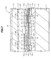
- Fig. 7 is a schematic cross sectional view of a solid state image pickup device 120 of the second embodiment.
- constituent elements common to those shown in Fig. 6 are represented by identical reference numerals and the description thereof is omitted.
- a color filter array 110 In the solid state image pickup device 120, a color filter array 110, a second planarizing film 115, and a spectral device 90 are stacked in this order on a first planarizing film 80.
- the other structures are similar to those of the solid state image pickup device 100.
- the first planarizing film 80 is preferably made as thin as possible.
- the color filter array 110 prevents light other than desired light from entering each photoelectric conversion element 10.
- a red filter 110R is disposed above the photoelectric conversion element 10 upon which red light spectroscopically split by the spectral device 90 is to be incident.
- a green filter 110G is disposed above the photoelectric conversion element 10 to which green light is to be applied.
- a blue filter 110B is disposed above the photoelectric conversion element 10 to which blue light is to be applied.
- Each of color filters 110R, 110G and 110B may be disposed above each photoelectric conversion element or a stripe shaped color filter may be disposed above each photoelectric conversion element column.
- the second planarizing film 115 is formed by spin coating light transmissive organic material such as photoresist.
- the thickness of the second planarizing film 115 is selected so that red, green and blue light fluxes spectroscopically split by the spectral device 90 enter the light reception planes of desired photoelectric conversion elements 10 as much as possible.
- the solid state image pickup device 120 constructed as above provides similar effects to those of the solid state image pickup device 100 of the first embodiment. Since the color filter array 110 is formed in addition to the spectral device 90, an image having a high quality can easily be obtained by using output signals (pixel signals) of the solid state image pickup device 120.
- Fig. 8 is a schematic cross sectional view of a solid state image pickup device 140 of the third embodiment.
- constituent elements common to those shown in Fig. 7 are represented by identical reference numerals and the description thereof is omitted.
- a predetermined region of a passivation film 75A above each photoelectric conversion element 10 functions as a micro lens 75a.
- the other structures are similar to the solid image pickup device 120.
- the passivation film 75A can be formed by the following method for example.
- a transparent material layer such as a silicon nitride layer which can be used as the material of the passivation film and has a thickness sufficient for forming micro lenses 75a.
- a micro lens array having a predetermined shape is formed on this transparent material layer.
- the micro lens array is formed by segmenting a transparent resin (inclusive of photoresist) layer into areas having a predetermined shape by photolithography or the like, melting each area by heat treatment to round the corners of each area by surface tension, and thereafter cooling each area. Each area is molded into a micro lens.
- the passivation film 75A having the areas functioning as the micro lens 75a can be obtained.
- the solid state image pickup device 140 constructed as above provides similar effects to those of the solid state image pickup device 120 of the second embodiment. Since the micro lens 75a is formed above each photoelectric conversion element 10, the amount of light of each color incident upon the photoelectric conversion element 10 can be increased. The sensitivity of the solid state image pickup device can further be increased.
- Fig. 9 is a schematic plan view showing the layout of photoelectric conversion elements 10, vertical charge transfer units 20, a horizontal charge transfer unit 40 and a charge detector circuit 50, respectively of the solid state image pickup device 160 of the fourth embodiment.
- the solid state image pickup device 160 has the structure similar to the solid state image pickup device 100 of the first embodiment, excepting that a number of photoelectric conversion elements 10 are disposed in a pixel shift layout, that each vertical charge transfer unit 20 has a zigzag shape, and the spectral characteristics of the spectral device to be described later.
- the "pixel shift layout" of a number of photoelectric conversion elements used in this specification is the layout that each photoelectric conversion element in the odd number photoelectric conversion element column (row) is shifted in the column (row) direction by about a half pitch of photoelectric conversion elements in the column (row) direction from each photoelectric conversion element in the even number photoelectric conversion element, and that each photoelectric conversion element column contains only even or odd photoelectric conversion elements.
- the "pixel shift layout” is one of the layouts wherein a number of photoelectric conversion elements are disposed in a matrix shape having a plurality of rows and columns.
- each vertical charge transfer unit 20 has a zigzag shape as shown in Fig. 9.
- Fig. 10 is a schematic top view showing the solid state image pickup device 160.
- a spectral device 190 is disposed at the top of the solid state image pickup device 160.
- the spectral device 190 has five spectral regions 190A to 190E.
- the plan shape of each of the spectral regions 190A to 190E is a rhomboid having a diagonal line extending along the photoelectric conversion element row direction and a diagonal line extending along the photoelectric conversion element column direction.
- Each spectral region corresponds to four adjacent photoelectric conversion elements 10.
- the four photoelectric conversion elements corresponding to each spectral region accumulate charges corresponding to the signals (pixel signals of four kinds) of the minimum unit necessary for interpolation.
- the interpolation process is executed when pixel signals for image reproduction are generated from output signals (pixel signals) of the solid state image pickup device 160.
- Fig. 11 is a perspective view showing the spectral characteristics of the spectral region 190C shown in Fig. 10.
- the spectral device 190C spectroscopically splits red, green and blue light fluxes L R , L G and L B contained in incident light L toward different directions.
- the red light L R is spectroscopically split toward a surface region R r of the semiconductor substrate 1
- the green light L G is spectroscopically split toward a surface region R g
- the blue light L B is spectroscopically split toward a surface region R b .
- the spectral characteristics of the spectral regions 190A, 190B, 190D and 190E have similar characteristics to those of the spectral region 190C.
- the light reception plane of the photoelectric conversion element 10A corresponding to the spectral region 190C is positioned in a region R g1
- the light reception plane of the photoelectric conversion element 10B is positioned in a region R g2
- the light reception plane of the photoelectric conversion element 10C is positioned in a region R b
- the light reception plane of the photoelectric conversion element 10D is positioned in a region R r .
- the positional relationship between four photoelectric conversion elements 10 and each of the other spectral regions 190A, 190B, 190D and 190E is the same as the positional relationship between the photoelectric conversion elements 10A to 10D and the spectral region 190C.
- the spectral device 190 is preferably a holographic device.
- the spectral device 190 made of a holographic device can be manufactured by a method similar to that already described with Fig. 5.
- two slits are used to obtain the spectral device capable of spectroscopically splitting green light toward two areas as shown in Fig. 11.
- This solid state image pickup device 160 has similar effects to those of the solid state image pickup device 100 of the first embodiment.
- a color filter array may be disposed under the spectral device, similar to the solid state image pickup device 120 of the second embodiment.
- a passivation film may be formed in which the passivation film region above each photoelectric conversion element functions as a micro lens.
- a micro lens array manufacture method, solid state image pickup devices and their manufacture methods have been described above.
- the invention is not limited only to the above embodiments.
- the structures of the solid state image pickup device other than the spectral device may be changed in various ways depending upon the application, performance and the like.
- two or three vertical transfer electrodes may be formed for each photoelectric conversion element row.
- Fig. 12 is a schematic diagram showing a solid state image pickup device 100A wherein a number of photoelectric conversion elements 10 are disposed in a tetragonal matrix shape and each vertical charge transfer unit 20 has two first and second vertical transfer electrodes 25a and 25b per one photoelectric conversion element row.
- Each vertical charge transfer unit 20 is constituted of four-phase drive type CCDs which are driven by four-phase drive signals ⁇ V1 to ⁇ V4 supplied via wiring lines WL v1 to WL v4 .
- Each vertical charge transfer channel 23 extends linearly along the photoelectric conversion element column.
- the first vertical transfer electrode 25a is disposed at the upstream position of the photoelectric conversion element row, traversing the vertical charge transfer channels 23 as viewed in plan, and the second vertical transfer electrode 25b is disposed at the downstream position of the photoelectric conversion element row.
- the first and second vertical charge transfer electrodes 25a and 25b extend along the photoelectric conversion element row, and one ends of the second vertical transfer electrode 25b overlap one end of the first vertical transfer electrode 25a above the vertical charge transfer channel 23.
- a plurality of vertical transfer electrodes e.g., three vertical transfer electrodes, are disposed at the downstream position of the most downstream second vertical transfer electrode 25b.
- the solid state image pickup device 100A may have a second electrically insulating layer, a light shielding film, an interlayer insulating film, a passivation film, a first planarizing film sequentially disposed over a semiconductor substrate 1, and a spectral device formed on the first planarizing film. Similar to the solid state image pickup device 120 of the second embodiment, a color filter array may be formed under the spectral device. Similar to the solid state image pickup device 140 of the third embodiment, a passivation film may be formed wherein a region of the passivation film above a photoelectric conversion element functions as a micro lens.
- Fig. 13 is a schematic diagram showing a solid state image pickup device 160A wherein a number of photoelectric conversion elements are disposed in the pixel shift layout and each vertical charge transfer unit 20 has first and second vertical transfer electrodes 25a and 25b per one photoelectric conversion element row.
- each vertical charge transfer channel 23 extends in a zigzag way along the photoelectric conversion element column and each of the first and second vertical transfer electrodes 25a and 25b extends in a zigzag way along the photoelectric conversion element row.
- the solid state image pickup device 160A may also have the above-described lamination structure and additional elements.
- the number of phases of drive signals for driving the vertical and horizontal charge transfer units is determined in accordance with the number of vertical transfer electrodes per one photoelectric conversion element row, the number of horizontal transfer electrodes per one vertical charge transfer unit, or the methods of driving the vertical or horizontal charge transfer units.
- the horizontal charge transfer unit may be formed by disposing two or more horizontal transfer electrodes per one vertical charge transfer unit.
- the spectral device 90 described with Figs. 2 and 3 and the spectral device 190 described with Figs. 10 and 11 may be applied to a MOS solid state image pickup device.
- Fig. 14A is a schematic diagram showing the layout of photoelectric conversion elements and an output signal generator unit of a MOS solid state image pickup device used as an area image sensor.
- the solid state image pickup device 300 has a number of photoelectric conversion elements 210 disposed on the surface of a semiconductor substrate 201 in a square matrix shape having a plurality of rows and columns. A switching circuit (not shown) is formed for each photoelectric conversion element 210.
- An output signal line 230 is formed along the photoelectric conversion element column for each photoelectric conversion element column.
- a load transistor 240 is connected to each output signal line 230.
- the output signal lines 230 are connected to the signal generator unit 250.
- a row read scanner 260 and a row reset scanner 265 are disposed on the semiconductor substrate 201.
- the row read scanner 260 controls the operation of each switching circuit to establish an electrical connection between each photoelectric conversion element 210 and output signal line 230.
- the row reset scanner 265 controls the operation of each switching circuit to drain charges accumulated in the photoelectric conversion element 210.
- a row select signal line 224 and a reset signal line 227 are disposed for each photoelectric conversion element column.
- a power supply voltage line 225 is disposed for each photoelectric conversion element row or column. The signal lines and voltage line can be electrically connected to each switching circuit.
- a controller 270 is disposed on the semiconductor substrate 201 to control the operations of the signal generator unit 250, row read scanner 260 and row reset scanner 265.
- Fig. 14B shows an example of the switching circuit.
- the switching circuit 220 includes an output transistor 221, a row select transistor 222 and a reset transistor 223. These transistors are, for example, MOS transistors.
- the output transistor 221 and row select transistor 222 are serially connected, the photoelectric conversion element 210 is connected to the gate of the output transistor 222, and the row select signal line 224 is connected to the gate of the row select transistor 222.
- the remaining end of the output transistor is connected to the power supply voltage line 225 and the remaining end of the row select transistor 222 is connected to the output signal line 230.
- the reset transistor 223 is connected to a wiring line 226 interconnecting the output transistor 222 and photoelectric conversion element 210, and to the power supply voltage line 225.
- a reset signal line 227 is connected to the gate of the reset transistor 223.
- the switching circuit 220, output signal line 230, load transistor 240, signal generator unit 250, row read scanner 260 and row reset scanner 265 constitute an output signal generator unit.
- the row select transistor 222 connected to the row select signal line 224 turns on.
- the output transistor 221 is therefore electrically connected to the output signal line 230.
- the voltage applied to the gate of the output transistor 221 changes in accordance with the amount of charges accumulated in the photoelectric conversion element 210 connected to the output transistor 221. Therefore, the drain current flowing through the output transistor 221 changes in accordance with the amount of charges accumulated in the photoelectric conversion element 210.
- the row select transistor 222 turns on, an electric signal corresponding to the amount of charges accumulated in the photoelectric conversion element 210 is output to the output signal line 230.
- the reset transistor 223 connected to the reset signal line 227 turns on.
- the photoelectric conversion element 210 corresponding to the reset transistor 223 is therefore connected to the power supply voltage line 225 and charges accumulated in the photoelectric conversion element 210 are drained to the power supply voltage line 225.
- the MOS solid state image pickup device 300 may have a second electrically insulating layer, a light shielding film, an interlayer insulating film, a passivation film, a first planarizing film sequentially disposed over the semiconductor substrate 201, and a spectral device formed on the first planarizing film. Similar to the solid state image pickup device 120 of the second embodiment, a color filter array may be formed under the spectral device. Similar to the solid state image pickup device 140 of the third embodiment, a passivation film may be formed wherein a region of the passivation film above a photoelectric conversion element functions as a micro lens.
- the number of spectral regions of a spectral device and its layout can be determined in accordance with the number of photoelectric conversion elements formed in a semiconductor substrate and their layout, a method of driving a vertical charge transfer unit, a method of processing a signal in an image pickup apparatus using a solid state image pickup device, and the like.
- each spectral region as viewed in plan is preferably larger than a sum of areas of two photoelectric conversion elements as viewed in plan. If light spectroscopically split on each photoelectric conversion element is the light incident upon the spectral device far apart from the photoelectric conversion element, the quality of an image reproduced from output signals (pixel signals) of the solid state image pickup device is degraded.
- each spectral region of a spectral device it is preferable to form each spectral region of a spectral device so that light spectroscopically split on one photoelectric conversion element corresponding to the spectral region is the light incident upon the spectral device above another photoelectric conversion element in the range of about two rows and three columns as counted from the photoelectric conversion element.
- a spectral device is made of a diffraction optical element having a diffraction grating pattern
- shape of the diffraction grating pattern to be formed on each spectral region can be determined in accordance with the target spectral characteristics.
- a method of manufacturing a spectral device can be selected in accordance with the target spectral characteristics, productivity and the like.
- a solid state image pickup device may be made of a discrete spectral device separated from other constituent elements.
- the underlying layer of the spectral device integrated with other constituent elements can be omitted.
- members for supporting the spectral device at a predetermined position are required.
- a glue structure of a spectral device glued to a predetermined underlying layer may be used as the structure of the solid state image pickup device.
- the degree of freedom of selecting material of the spectral device can be increased.
Landscapes
- Physics & Mathematics (AREA)
- General Physics & Mathematics (AREA)
- Power Engineering (AREA)
- Spectroscopy & Molecular Physics (AREA)
- Engineering & Computer Science (AREA)
- Condensed Matter Physics & Semiconductors (AREA)
- Computer Hardware Design (AREA)
- Microelectronics & Electronic Packaging (AREA)
- Electromagnetism (AREA)
- Optics & Photonics (AREA)
- Solid State Image Pick-Up Elements (AREA)
- Diffracting Gratings Or Hologram Optical Elements (AREA)
- Transforming Light Signals Into Electric Signals (AREA)
- Light Receiving Elements (AREA)
- Color Television Image Signal Generators (AREA)
Applications Claiming Priority (2)
| Application Number | Priority Date | Filing Date | Title |
|---|---|---|---|
| JP2002045011 | 2002-02-21 | ||
| JP2002045011A JP3742775B2 (ja) | 2002-02-21 | 2002-02-21 | 固体撮像素子 |
Publications (2)
| Publication Number | Publication Date |
|---|---|
| EP1339237A2 true EP1339237A2 (fr) | 2003-08-27 |
| EP1339237A3 EP1339237A3 (fr) | 2006-06-07 |
Family
ID=27655317
Family Applications (1)
| Application Number | Title | Priority Date | Filing Date |
|---|---|---|---|
| EP03003101A Withdrawn EP1339237A3 (fr) | 2002-02-21 | 2003-02-12 | Dispositif de prise d'images à l'état solide |
Country Status (3)
| Country | Link |
|---|---|
| US (1) | US7202896B2 (fr) |
| EP (1) | EP1339237A3 (fr) |
| JP (1) | JP3742775B2 (fr) |
Cited By (4)
| Publication number | Priority date | Publication date | Assignee | Title |
|---|---|---|---|---|
| WO2007039559A1 (fr) * | 2005-10-01 | 2007-04-12 | Chromasens Gmbh | Dispositif pour prendre plusieurs images d'objets en forme de disques |
| WO2011063939A1 (fr) * | 2009-11-27 | 2011-06-03 | Carl Zeiss Ag | Capteur d'images, dispositif de génération d'images ainsi que spectroscope pour la spectroscopie à résolution spatiale |
| WO2013028243A1 (fr) * | 2011-08-24 | 2013-02-28 | Aptina Imaging Corporation | Systèmes d'imagerie à super-résolution |
| EP3812721A1 (fr) * | 2019-10-24 | 2021-04-28 | Samsung Electronics Co., Ltd. | Capteur d'imagerie hyperspectrale et appareil de capture d'images hyperspectrales le comprenant |
Families Citing this family (26)
| Publication number | Priority date | Publication date | Assignee | Title |
|---|---|---|---|---|
| EP1533651A4 (fr) * | 2003-03-28 | 2007-03-07 | Seiko Epson Corp | Modulateur de lumiere spatial, projecteur l'utilisant, procede de fabrication d'un element a structure fine utilise dans le modulateur et element a structure fine fabrique selon ce procede |
| JP4450597B2 (ja) * | 2003-09-24 | 2010-04-14 | 東京エレクトロン株式会社 | マイクロレンズの形成方法 |
| JP2005286115A (ja) * | 2004-03-30 | 2005-10-13 | Fuji Film Microdevices Co Ltd | 光電変換膜積層型固体撮像装置及びその駆動方法並びにデジタルカメラ |
| JP4838501B2 (ja) * | 2004-06-15 | 2011-12-14 | 富士通セミコンダクター株式会社 | 撮像装置及びその製造方法 |
| ATE400062T1 (de) * | 2005-06-30 | 2008-07-15 | Suisse Electronique Microtech | Farbbildaufnahmesensor |
| JP4667143B2 (ja) * | 2005-07-07 | 2011-04-06 | 富士フイルム株式会社 | 固体撮像素子 |
| CN1971927B (zh) * | 2005-07-21 | 2012-07-18 | 索尼株式会社 | 物理信息获取方法、物理信息获取装置和半导体器件 |
| JP2007220832A (ja) * | 2006-02-15 | 2007-08-30 | Matsushita Electric Ind Co Ltd | 固体撮像装置及びカメラ |
| WO2009019818A1 (fr) * | 2007-08-06 | 2009-02-12 | Panasonic Corporation | Dispositif de détection de lumière pour un traitement de l'image |
| US20090096900A1 (en) * | 2007-10-11 | 2009-04-16 | Chin-Poh Pang | Image sensor device |
| US8384818B2 (en) | 2008-06-18 | 2013-02-26 | Panasonic Corporation | Solid-state imaging device including arrays of optical elements and photosensitive cells |
| WO2010016195A1 (fr) * | 2008-08-05 | 2010-02-11 | パナソニック株式会社 | Dispositif de photodétection utilisé pour un capteur d'image |
| US8289422B2 (en) * | 2009-01-14 | 2012-10-16 | Panasonic Corporation | Image capture device |
| KR101788124B1 (ko) * | 2010-07-07 | 2017-10-20 | 삼성전자 주식회사 | 후면 조사형 이미지 센서 및 그 제조 방법 |
| US9971078B2 (en) * | 2013-03-05 | 2018-05-15 | Rambus Inc. | Phase gratings with odd symmetry for high-resolution lensless optical sensing |
| US9515113B2 (en) | 2013-08-27 | 2016-12-06 | Rambus Inc. | Optical sensing of nearby scenes with tessellated phase anti-symmetric gratings |
| KR102501643B1 (ko) * | 2015-09-24 | 2023-02-20 | 삼성전자주식회사 | 고굴절률 광학 기능층을 포함하는 광학 장치 및 상기 광학 장치의 제조 방법 |
| US20220284857A1 (en) * | 2019-08-23 | 2022-09-08 | Boe Technology Group Co., Ltd. | Display device and manufacturing method thereof |
| WO2021059409A1 (fr) * | 2019-09-25 | 2021-04-01 | 日本電信電話株式会社 | Élément de capture d'image et dispositif de capture d'image |
| CN114556569A (zh) * | 2019-10-09 | 2022-05-27 | 日本电信电话株式会社 | 分光元件阵列、摄像元件以及摄像装置 |
| CN112701132A (zh) | 2019-10-23 | 2021-04-23 | 三星电子株式会社 | 图像传感器和包括该图像传感器的电子装置 |
| EP4398304A2 (fr) | 2019-10-23 | 2024-07-10 | Samsung Electronics Co., Ltd. | Capteur d'image comprenant un réseau de lentilles de séparation de couleurs et dispositif électronique comprenant le capteur d'image |
| JP7446785B2 (ja) * | 2019-11-18 | 2024-03-11 | 株式会社ジャパンディスプレイ | 検出装置及び表示装置 |
| JP7446786B2 (ja) * | 2019-11-18 | 2024-03-11 | 株式会社ジャパンディスプレイ | 検出装置及び表示装置 |
| US20230239552A1 (en) * | 2020-05-21 | 2023-07-27 | Nippon Telegraph And Telephone Corporation | Image sensor and imaging device |
| JP2022121757A (ja) * | 2021-02-05 | 2022-08-22 | ブリルニクスジャパン株式会社 | 固体撮像装置、固体撮像装置の製造方法、および電子機器 |
Citations (6)
| Publication number | Priority date | Publication date | Assignee | Title |
|---|---|---|---|---|
| EP0583150A1 (fr) * | 1992-08-11 | 1994-02-16 | Sharp Kabushiki Kaisha | Dispositif d'affichage |
| US5481383A (en) * | 1992-11-13 | 1996-01-02 | Canon Kabushiki Kaisha | Color image reader |
| US5497269A (en) * | 1992-06-25 | 1996-03-05 | Lockheed Missiles And Space Company, Inc. | Dispersive microlens |
| US5529936A (en) * | 1992-09-30 | 1996-06-25 | Lsi Logic Corporation | Method of etching a lens for a semiconductor solid state image sensor |
| EP0750207A2 (fr) * | 1995-06-19 | 1996-12-27 | Eastman Kodak Company | Matrice optique diffractive pour la séparation des couleurs et capteur d'images |
| EP1091567A2 (fr) * | 1999-10-07 | 2001-04-11 | Fuji Photo Film Co., Ltd. | Dispositif à transfert de charges, dispositif de prise d'images à l'état solide l'utilisant et méthode de commande |
Family Cites Families (13)
| Publication number | Priority date | Publication date | Assignee | Title |
|---|---|---|---|---|
| GB1529711A (en) * | 1975-07-01 | 1978-10-25 | Rca Corp | Optical etc phase filters producing near-field patterns |
| JPS60204170A (ja) * | 1984-03-29 | 1985-10-15 | Toshiba Corp | 画像読取り装置 |
| JPH03226067A (ja) * | 1990-01-30 | 1991-10-07 | Canon Inc | カラー画像読取り装置 |
| JPH0821703B2 (ja) * | 1990-07-17 | 1996-03-04 | 株式会社東芝 | 固体撮像素子 |
| JP2570946B2 (ja) * | 1992-06-25 | 1997-01-16 | キヤノン株式会社 | カラー画像読取装置 |
| JP3506144B2 (ja) * | 1992-10-19 | 2004-03-15 | ソニー株式会社 | 画像表示装置及び表示デバイス用光学フィルタ |
| US5471515A (en) * | 1994-01-28 | 1995-11-28 | California Institute Of Technology | Active pixel sensor with intra-pixel charge transfer |
| US5682265A (en) * | 1994-02-18 | 1997-10-28 | Massachusetts Institute Of Technology | Diffractive microstructures for color separation and fusing |
| JP3724882B2 (ja) * | 1996-08-14 | 2005-12-07 | シャープ株式会社 | カラー固体撮像装置 |
| US6137535A (en) * | 1996-11-04 | 2000-10-24 | Eastman Kodak Company | Compact digital camera with segmented fields of view |
| JPH11295513A (ja) | 1998-04-14 | 1999-10-29 | Minolta Co Ltd | 色分光素子を有する装置 |
| TW475334B (en) * | 2000-07-14 | 2002-02-01 | Light Opto Electronics Co Ltd | High light-sensing efficiency image sensor apparatus and method of making the same |
| US6738171B1 (en) * | 2001-11-21 | 2004-05-18 | Micron Technology, Inc. | Color filter array and microlens array having holographic optical elements |
-
2002
- 2002-02-21 JP JP2002045011A patent/JP3742775B2/ja not_active Expired - Fee Related
-
2003
- 2003-02-11 US US10/361,624 patent/US7202896B2/en not_active Expired - Fee Related
- 2003-02-12 EP EP03003101A patent/EP1339237A3/fr not_active Withdrawn
Patent Citations (6)
| Publication number | Priority date | Publication date | Assignee | Title |
|---|---|---|---|---|
| US5497269A (en) * | 1992-06-25 | 1996-03-05 | Lockheed Missiles And Space Company, Inc. | Dispersive microlens |
| EP0583150A1 (fr) * | 1992-08-11 | 1994-02-16 | Sharp Kabushiki Kaisha | Dispositif d'affichage |
| US5529936A (en) * | 1992-09-30 | 1996-06-25 | Lsi Logic Corporation | Method of etching a lens for a semiconductor solid state image sensor |
| US5481383A (en) * | 1992-11-13 | 1996-01-02 | Canon Kabushiki Kaisha | Color image reader |
| EP0750207A2 (fr) * | 1995-06-19 | 1996-12-27 | Eastman Kodak Company | Matrice optique diffractive pour la séparation des couleurs et capteur d'images |
| EP1091567A2 (fr) * | 1999-10-07 | 2001-04-11 | Fuji Photo Film Co., Ltd. | Dispositif à transfert de charges, dispositif de prise d'images à l'état solide l'utilisant et méthode de commande |
Cited By (5)
| Publication number | Priority date | Publication date | Assignee | Title |
|---|---|---|---|---|
| WO2007039559A1 (fr) * | 2005-10-01 | 2007-04-12 | Chromasens Gmbh | Dispositif pour prendre plusieurs images d'objets en forme de disques |
| WO2011063939A1 (fr) * | 2009-11-27 | 2011-06-03 | Carl Zeiss Ag | Capteur d'images, dispositif de génération d'images ainsi que spectroscope pour la spectroscopie à résolution spatiale |
| WO2013028243A1 (fr) * | 2011-08-24 | 2013-02-28 | Aptina Imaging Corporation | Systèmes d'imagerie à super-résolution |
| US8866951B2 (en) | 2011-08-24 | 2014-10-21 | Aptina Imaging Corporation | Super-resolution imaging systems |
| EP3812721A1 (fr) * | 2019-10-24 | 2021-04-28 | Samsung Electronics Co., Ltd. | Capteur d'imagerie hyperspectrale et appareil de capture d'images hyperspectrales le comprenant |
Also Published As
| Publication number | Publication date |
|---|---|
| US20030156210A1 (en) | 2003-08-21 |
| JP3742775B2 (ja) | 2006-02-08 |
| JP2003243640A (ja) | 2003-08-29 |
| US7202896B2 (en) | 2007-04-10 |
| EP1339237A3 (fr) | 2006-06-07 |
Similar Documents
| Publication | Publication Date | Title |
|---|---|---|
| US7202896B2 (en) | Solid state image pickup device having spectral device | |
| US8409907B2 (en) | Method for manufacturing information aquiring semiconductor device | |
| US7271836B2 (en) | Solid state image pickup device capable of draining unnecessary charge and driving method thereof | |
| US7411232B2 (en) | Semiconductor photodetecting device and method of manufacturing the same | |
| US6903391B2 (en) | Solid state image pickup device | |
| EP1331670B1 (fr) | Dispositif de prise de vues à l'état solide à deux zones photosensibles par pixel | |
| TWI425629B (zh) | 固態影像拾取裝置及其製造方法,影像拾取裝置及電子裝置 | |
| US8072007B2 (en) | Backside-illuminated imaging device | |
| US6933976B1 (en) | Solid-state image pickup device | |
| US7719040B2 (en) | Solid-state imaging device | |
| US7372491B2 (en) | CMOS image sensor | |
| EP1091411B1 (fr) | Capteur d'images à l'état solide et procédé de commande | |
| US7154549B2 (en) | Solid state image sensor having a single-layered electrode structure | |
| US6707495B1 (en) | Solid-state imaging device and a method of reading a signal charge in a solid-state imaging device which can reduce smear and can provide an excellent image characteristic | |
| US6806904B1 (en) | Solid-state image pickup device | |
| US6545304B2 (en) | Solid-state image pickup device | |
| US7091463B2 (en) | Solid state image pickup device with polysilicon transfer electrodes | |
| US7579207B2 (en) | Solid-state imaging device, method of producing the same and camera | |
| JPWO2006046421A1 (ja) | 固体撮像装置、固体撮像装置の製造方法及びカメラ | |
| US20050145889A1 (en) | Solid state image pickup device and its manufacture method | |
| JP3795808B2 (ja) | 固体撮像素子およびこれを用いた撮像装置 | |
| US8399946B1 (en) | Solid-state imaging device and manufacturing method thereof | |
| JP2008047608A (ja) | 単板式カラー固体撮像素子 | |
| JP2001111025A (ja) | 固体撮像装置 | |
| JP2002359365A (ja) | 固体撮像装置 |
Legal Events
| Date | Code | Title | Description |
|---|---|---|---|
| PUAI | Public reference made under article 153(3) epc to a published international application that has entered the european phase |
Free format text: ORIGINAL CODE: 0009012 |
|
| AK | Designated contracting states |
Designated state(s): AT BE BG CH CY CZ DE DK EE ES FI FR GB GR HU IE IT LI LU MC NL PT SE SI SK TR |
|
| AX | Request for extension of the european patent |
Extension state: AL LT LV MK RO |
|
| PUAL | Search report despatched |
Free format text: ORIGINAL CODE: 0009013 |
|
| AK | Designated contracting states |
Kind code of ref document: A3 Designated state(s): AT BE BG CH CY CZ DE DK EE ES FI FR GB GR HU IE IT LI LU MC NL PT SE SI SK TR |
|
| AX | Request for extension of the european patent |
Extension state: AL LT LV MK RO |
|
| 17P | Request for examination filed |
Effective date: 20060517 |
|
| 17Q | First examination report despatched |
Effective date: 20061222 |
|
| AKX | Designation fees paid |
Designated state(s): DE FR GB |
|
| RAP1 | Party data changed (applicant data changed or rights of an application transferred) |
Owner name: FUJIFILM CORPORATION |
|
| GRAP | Despatch of communication of intention to grant a patent |
Free format text: ORIGINAL CODE: EPIDOSNIGR1 |
|
| STAA | Information on the status of an ep patent application or granted ep patent |
Free format text: STATUS: THE APPLICATION IS DEEMED TO BE WITHDRAWN |
|
| 18D | Application deemed to be withdrawn |
Effective date: 20110823 |