EP1334060B1 - Composant micromecanique et procede de production correspondant - Google Patents
Composant micromecanique et procede de production correspondant Download PDFInfo
- Publication number
- EP1334060B1 EP1334060B1 EP01992685A EP01992685A EP1334060B1 EP 1334060 B1 EP1334060 B1 EP 1334060B1 EP 01992685 A EP01992685 A EP 01992685A EP 01992685 A EP01992685 A EP 01992685A EP 1334060 B1 EP1334060 B1 EP 1334060B1
- Authority
- EP
- European Patent Office
- Prior art keywords
- layer
- produced
- regions
- substrate
- substrate material
- Prior art date
- Legal status (The legal status is an assumption and is not a legal conclusion. Google has not performed a legal analysis and makes no representation as to the accuracy of the status listed.)
- Expired - Lifetime
Links
Images


Classifications
-
- B—PERFORMING OPERATIONS; TRANSPORTING
- B81—MICROSTRUCTURAL TECHNOLOGY
- B81C—PROCESSES OR APPARATUS SPECIALLY ADAPTED FOR THE MANUFACTURE OR TREATMENT OF MICROSTRUCTURAL DEVICES OR SYSTEMS
- B81C1/00—Manufacture or treatment of devices or systems in or on a substrate
- B81C1/00436—Shaping materials, i.e. techniques for structuring the substrate or the layers on the substrate
- B81C1/00555—Achieving a desired geometry, i.e. controlling etch rates, anisotropy or selectivity
- B81C1/00595—Control etch selectivity
-
- B—PERFORMING OPERATIONS; TRANSPORTING
- B81—MICROSTRUCTURAL TECHNOLOGY
- B81B—MICROSTRUCTURAL DEVICES OR SYSTEMS, e.g. MICROMECHANICAL DEVICES
- B81B2201/00—Specific applications of microelectromechanical systems
- B81B2201/02—Sensors
- B81B2201/0228—Inertial sensors
- B81B2201/0235—Accelerometers
-
- B—PERFORMING OPERATIONS; TRANSPORTING
- B81—MICROSTRUCTURAL TECHNOLOGY
- B81B—MICROSTRUCTURAL DEVICES OR SYSTEMS, e.g. MICROMECHANICAL DEVICES
- B81B2201/00—Specific applications of microelectromechanical systems
- B81B2201/03—Microengines and actuators
- B81B2201/036—Micropumps
-
- B—PERFORMING OPERATIONS; TRANSPORTING
- B81—MICROSTRUCTURAL TECHNOLOGY
- B81C—PROCESSES OR APPARATUS SPECIALLY ADAPTED FOR THE MANUFACTURE OR TREATMENT OF MICROSTRUCTURAL DEVICES OR SYSTEMS
- B81C2201/00—Manufacture or treatment of microstructural devices or systems
- B81C2201/01—Manufacture or treatment of microstructural devices or systems in or on a substrate
- B81C2201/0101—Shaping material; Structuring the bulk substrate or layers on the substrate; Film patterning
- B81C2201/0111—Bulk micromachining
- B81C2201/0114—Electrochemical etching, anodic oxidation
-
- B—PERFORMING OPERATIONS; TRANSPORTING
- B81—MICROSTRUCTURAL TECHNOLOGY
- B81C—PROCESSES OR APPARATUS SPECIALLY ADAPTED FOR THE MANUFACTURE OR TREATMENT OF MICROSTRUCTURAL DEVICES OR SYSTEMS
- B81C2201/00—Manufacture or treatment of microstructural devices or systems
- B81C2201/01—Manufacture or treatment of microstructural devices or systems in or on a substrate
- B81C2201/0101—Shaping material; Structuring the bulk substrate or layers on the substrate; Film patterning
- B81C2201/0111—Bulk micromachining
- B81C2201/0115—Porous silicon
-
- B—PERFORMING OPERATIONS; TRANSPORTING
- B81—MICROSTRUCTURAL TECHNOLOGY
- B81C—PROCESSES OR APPARATUS SPECIALLY ADAPTED FOR THE MANUFACTURE OR TREATMENT OF MICROSTRUCTURAL DEVICES OR SYSTEMS
- B81C2201/00—Manufacture or treatment of microstructural devices or systems
- B81C2201/01—Manufacture or treatment of microstructural devices or systems in or on a substrate
- B81C2201/0101—Shaping material; Structuring the bulk substrate or layers on the substrate; Film patterning
- B81C2201/0128—Processes for removing material
- B81C2201/013—Etching
- B81C2201/0135—Controlling etch progression
- B81C2201/0136—Controlling etch progression by doping limited material regions
-
- B—PERFORMING OPERATIONS; TRANSPORTING
- B81—MICROSTRUCTURAL TECHNOLOGY
- B81C—PROCESSES OR APPARATUS SPECIALLY ADAPTED FOR THE MANUFACTURE OR TREATMENT OF MICROSTRUCTURAL DEVICES OR SYSTEMS
- B81C2203/00—Forming microstructural systems
- B81C2203/01—Packaging MEMS
- B81C2203/0136—Growing or depositing of a covering layer
Definitions
- the present invention relates to a micromechanical component having a substrate made of a substrate material with a first doping, a micromechanical functional structure provided in the substrate and a covering layer for at least partially covering the micromechanical functional structure.
- the present invention also relates to a corresponding production method.
- any active function e.g. a sensor function, or passive function, e.g. a conductor track function to be understood.
- OMM surface micromechanics
- Analog Devices Analog Devices
- This problem can be avoided by using a sensor with the evaluation circuit on a separate chip, e.g.
- the OMM structures are covered by means of a second cap wafer.
- This type of packaging causes a high proportion of the cost of an OMM acceleration sensor. These costs are caused by the high area requirement of the sealing surface between cap wafer and sensor wafer and due to the complex structuring (2-3 masks, bulk micro-mechanics) of the cap wafer.
- FIG. 10 shows a schematic cross-sectional view of a known micromechanical component.
- 10 denotes a semiconductor substrate, OS a sacrificial layer, FE a functional plane having a micromechanical functional structure (e.g., an acceleration sensor), SG a seal glass, HO a cavity, and KW a cap wafer.
- a micromechanical functional structure e.g., an acceleration sensor
- SG a seal glass
- HO a cavity
- KW a cap wafer
- European Patent Application EP 0 747 684 A1 describes a method for forming a silicon structure in a cavity by anodizing, oxidizing and etching or by direct etching of porous silicon.
- a p-doped layer is introduced into a substrate and an n-doped layer is epitaxially deposited on the n-doped substrate.
- two contact areas are introduced, which contact the p-doped layer through the epitaxially deposited layer.
- the substrate is anodized to form porous silicon from the contact regions and the p-doped layer.
- the porous silicon is oxidized and the oxide is etched to form a cavity and a silicon structure.
- the direct etching of the porous silicon is also proposed.
- the inventive micromechanical device with the features of claim 1 and the manufacturing method according to claim 15 allow a simple and inexpensive production of a micromechanical device, eg an acceleration sensor, a micropump, a flow channel, a check valve, a flow standard, etc., using porous substrate material.
- a micromechanical device eg an acceleration sensor, a micropump, a flow channel, a check valve, a flow standard, etc., using porous substrate material.
- the micromechanical functional structure comprises regions of the substrate material with a second doping which are at least partially surrounded by a cavity, and the cover layer comprises a porous layer of the substrate material.
- the p-doped regions are readily etchable when the substrate is anodized, but the n-doped regions are not or only slightly etchable on the surface.
- a closure layer for closing the pores of the porous layer is created, which encloses a predetermined atmosphere in the cavity.
- a predetermined atmosphere can be set under the membrane.
- the closure layer has an oxide layer formed on the porous layer.
- a support region for supporting the porous region is created over at least one of the regions of the substrate material with the second doping type.
- At least one of the regions of the substrate material with the second doping type completely detached from its environment.
- the cavity comprises a flow channel which can be connected through at least two rear side openings.
- the rear side openings are connected via a respective passage opening, which is formed in the area.
- a closure layer is provided for closing the pores of the porous layer and a detection device for piezoresistive detection of the flow velocity is created on the closure layer.
- a check valve device is provided above a corresponding passage opening within the flow channel, which has at least one of the regions of the substrate material with the second doping type, which is completely detached from its environment or resiliently connected to the substrate material.
- two non-return valve devices of different geometry are created above a corresponding passage opening; the porous layer is provided and the porous region with the sealing layer as a pump diaphragm is deflectable such that the volume of the cavity changes.
- the cavity comprises a circular inner flow channel and a concentric outer flow channel which are connected by radial passage openings in a separation region of the substrate material with the second doping type, wherein the inner flow channel is interrupted by a web and on one side the web has a rear side entry opening and a first rear side exit opening is created on the other side of the web, and wherein a second rear side exit opening is created in the outer flow channel; such that a medium flowing in through the rear side inlet opening is mass-specifically separable by the centrifugal force through the first and second rear side outlet openings.
- the substrate material is silicon.
- the regions of the substrate material with the second doping type are created at different depths in the substrate.
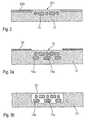
- FIG. 1a-c show schematic cross-sectional views for illustrating an embodiment of the production method according to the invention for producing a micromechanical component.
- 10 denotes a p-doped wafer substrate made of silicon, 15 n-doped regions in the substrate 10, 20 a metal mask and 21 metal mask openings.
- the n-doped regions are produced in the substrate 10 with standard semiconductor processes in the p-doped substrate 10. Examples of such processes are implantation methods in which the penetration depth can be determined with an appropriate distribution by adjusting the energy.
- the n-doped regions 15 are thus located at a certain depth below the substrate surface and, although not shown, may also be disposed on the substrate surface.
- the metal mask 20 could also include a nitride mask, an oxynitride mask, and the like. be used.
- the areas of the substrate 10 defined by the mask 20 are electrochemically etched by hydrofluoric acid (HF).
- HF hydrofluoric acid
- the porosity is controlled by the current density. Initially, a low current density is applied, creating a layer with low porosity. Subsequently, the current density is increased above a critical value.
- the hydrofluoric acid concentration can be reduced or other solutions that inhibit H 2 formation can be used.
- the pores in the lower region of the porous layer 30 become so large that the substrate material is etched out completely and the cavity 50 forms below a remaining porous layer 30. In this case we speak of electropolishing. The material removal takes place through the porous layer 30.
- the structure thus formed in the functional plane, formed by the region 15, comprises separated structures 60 and fixed structures 70, and in particular also structural elements which are connected by a support region 40 with the porous layer 30, thus forming a membrane support.
- the structures can therefore also be undercut in particular and thus freed (see reference numeral 60 in FIG. 1b).
- n and p react differently in the semiconductor substrate 10 to the electrochemical etching attack.
- the p-doped regions in the semiconductor substrate 10 can be anodized very well, whereas the n-doped regions 15 resist the etching attack very well.
- the buried n-doped regions 15 are therefore not attacked during the anodization.
- a possibly superficially formed porous film on the n-doped regions 15 can be removed by annealing in H 2 or by a short dip in silicon-etching solutions, eg TMAH, or KOH-containing solutions.
- the etching front runs around the n-doped regions 15 in this case.
- the pores of the porous silicon region 30, which delimit the cavity 50 upwardly, can be closed by different processes.
- a layer deposition with oxide, nitride, metal, epitaxy or the oxidation of the porous layer 30 to form the sealing layer 75 is possible.
- Annealing in H 2 can also lead to a vacuum-tight closure, for example of temperatures above 1000 ° C.
- the pressure conditions during the closing process determine the self-adjusting in cavity 50 internal pressure, H 2 can diffuse out by annealing.
- the structure shown in Figure 1c could serve as an acceleration sensor.
- the exempted Structures 60 oscillate at lateral accelerations, thereby periodically changing the distance between the released structures 60 and the stationary structures 70.
- the change in distance can be evaluated capacitively in a known manner by an interdigital capacitor. If a vacuum is to be enclosed under the sealing membrane consisting of the porous region 30 and the sealing layer 75, this can be stabilized by the said protective regions 40.
- micromechanical structures fabricated by this method may be used together with a corresponding integrated circuit, e.g. an evaluation circuit to be produced.
- a corresponding integrated circuit e.g. an evaluation circuit to be produced.
- an epitaxial layer can optionally be deposited on the porous region.
- the corresponding circuit components are produced for example in CMOS, bipolar or mixing processes.
- FIG. 2 shows a variant of the embodiment of the production method according to the invention according to FIG. 1.
- reference numeral 200 denotes a doping mask and 201 a doping mask opening.
- an n-doping is used as the mask 200 in this embodiment.
- the combination of an n-type doping as a mask and an additional mask layer on the doped substrate surface, for example nitride, is also possible.
- FIG. 3a, b show a further variant of the embodiment of the inventive manufacturing method according to FIG. 1.
- the n-doped regions 30 are provided at different depths. This is possible in particular by choosing different implantation energies. As a result, it is also possible to produce structures with very complex depth profiles.
- two different implantations have been carried out for producing the upper functional plane with the n-doped regions 15a and for producing the functional plane with the n-doped regions 15b. Otherwise, the method steps proceed as already described in detail with reference to FIGS. 1a-c.
- a further possibility to introduce the second functional level, after the implantation of the first functional level, is to apply an epitaxial layer, into which the second functional level is implanted.
- FIG. 4a-d show yet another variant of the embodiment of the inventive manufacturing method according to FIG. 1.
- FIG. 4a 80 designates trenches in the p-doped semiconductor substrate 10 in addition to the already introduced reference symbols. These trenches are introduced into the semiconductor substrate 10 in accordance with conventional techniques, for example by an etching technique in conjunction with a hard mask.
- n-doped overlay layer 90 e.g. Epitaxial silicon
- the trenches are filled by means of a filling material, e.g. Polysilicon, filled and planarized the resulting structure.
- a filling material e.g. Polysilicon
- This procedure of trenching, doping, filling and epitaxial deposition can be cyclically repeated to create complicated depth profiles.
- this variant for producing the n-doped regions by means of the trenches 80 and the covering layer 90 makes it possible to produce a very sharp doping profile with a high aspect ratio.
- the filler 100 may also be either n-doped or p-doped, depending on how the resulting structure is to look.
- FIG. 5a, b show a schematic representation of a micromechanical component according to a first embodiment of the present invention, namely Fig. 5a in cross-sectional view and Fig. 5b in plan view.
- Figure 5a, b illustrate an application as a branched flow channel with defined passage openings.
- the passage openings are provided as rear side openings 510, while the porous area 30 is hermetically sealed by a sealing layer 75.
- the n-doped regions 15 are used to limit the cavity 50 a downwards and thus as the bottom of the flow channel.
- the y-shaped structure of the flow channel can be achieved by an appropriate masking.
- passage openings 520 are provided, which are provided in the n-doped region 15 and ensure that when etching the rear side openings 510 from the back, the passages are not so large, which by the corresponding cup-shaped scrubnetprofil is indicated.
- the n-doped region 15 also acts as an etch stop for the etching from the rear side.
- an additional epitaxial layer is deposited and power components, eg power transistors, are realized thereon.
- the flow channel can conduct a cooling liquid or a cooling gas or another cooling medium, so that the power components are cooled from the back with good thermal coupling can. This would have the advantage over cooling from the front that the surface would not have to be protected from the cooling medium.
- the flow channel is preferably designed in meandering fashion or in other directions.
- FIG. 6a, b show a schematic representation of a micromechanical component according to a second embodiment of the present invention, specifically FIG. 6a in a cross-sectional view and FIG. 6b in a plan view.
- the structure shown in Figure 6a, b is a development of the structure shown in Figure 5a, b.
- piezoresistive resistance elements 630, 630 ' are provided on the sealing layer above the porous region 30.
- a different pressure thus results, which exposes the membrane and thus the piezoresistive resistors 630, 630 'to different levels of stress.
- the resulting change in resistance can be evaluated.
- the advantage here is that due to the supply of mass flow from the back no media protection of the resistive elements 630, 630 'is necessary.
- FIG. 7a, b show a schematic cross-sectional view of a micromechanical device according to a third embodiment of the present invention, specifically FIG. 7a with a micro-closure ball and FIG. 7b with a micro-closure plate.
- FIG. 7a denotes a micro-closure ball in FIGS. 7a and 740 a micro-closure plate in FIG. 7b, which forms a check valve together with through-opening 720 in the n-doped region 15b.
- the micro-closure ball 730 or the micro-closure plate 740 are produced simultaneously with the through-passage or passage opening 720 and ensure a sealing of the passage opening 720 at a reflux.
- FIG. 8a, b show a schematic representation of a micromechanical component according to a fourth embodiment of the present invention, specifically FIG. 8a in a cross-sectional view and FIG. 8b in a plan view.
- FIGS. 8a, b is a micropump.
- the membrane consisting of the porous region 30 and the sealing layer 75 is made thinner and deflectable in the direction MA.
- Such a deflection may e.g. be realized in that a magnetic layer is used as the sealing layer 75, which is deflectable by an electromagnet. Also conceivable are a thermal deflection of the membrane or an electrostatic deflection.
- the cavity 50d increases or decreases in terms of volume, and by using two different non-return valves 830, 830 ', a flow direction ST can be impressed.
- the check valve 830 is spherical and the check valve 830 'is ellipsoidal, which cooperates with an elliptical elongate opening.
- the check valve 830 ' closes off the right inlet, while liquid can flow past the check valve.
- liquid is sucked through the left passage opening.
- the left check valve 830 closes the round passage opening, while liquid can flow past the right pass valve 830 '.
- the sucked liquid is pushed out through the right passage.
- FIG. 9a, b show a schematic representation of a micromechanical component according to a fifth embodiment of the present invention, specifically FIG. 9a in cross-sectional view and FIG. 9b in plan view.
- the structure shown in Figure 9a, b represents a gas centrifuge.
- the gas centrifuge comprises a circular inner flow channel 50e and a concentric outer flow channel 50f, which are interconnected by radial passage openings 905 in a separation region 15 of the substrate material.
- the inner flow channel is interrupted by a web 910.
- On one side of the ridge is a rear side entry opening E, and on the other side of the ridge 910 a first back side exit opening A1 is provided.
- a second rear opening A2 is provided at the end.
- any micromechanical base materials such as germanium, can be used, and not only the exemplified silicon substrate.
- any sensor structures can be formed.
Landscapes
- Engineering & Computer Science (AREA)
- Physics & Mathematics (AREA)
- Geometry (AREA)
- Manufacturing & Machinery (AREA)
- Microelectronics & Electronic Packaging (AREA)
- Micromachines (AREA)
- Pressure Sensors (AREA)
Claims (23)
- Composant micromécanique comprenant :un substrat semi-conducteur (10) d'un matériau de substrat avec un premier type de dopage ;une structure fonctionnelle micromécanique réalisée dans le substrat semi-conducteur (10) ; etune couche de couverture (30) pour recouvrir au moins partiellement la structure fonctionnelle micromécanique ;caractérisé en ce que
la structure fonctionnelle micromécanique présente des zones (15 ; 15a ; 15b ; 15c ; 730 ; 740 ; 830) en matériau de substrat avec un deuxième type de dopage opposé, qui sont au moins partiellement entourées par un espace creux (50 ; 50a-f) ; et
la couche de couverture (30) est une couche poreuse (30) en matériau de substrat. - Composant micromécanique selon la revendication 1,
caractérisé en ce qu'
une couche de fermeture (75) est réalisée pour fermer les pores de la couche poreuse (30), qui enferme une atmosphère prédéterminée dans l'espace creux (50 ; 50a-f). - Composant micromécanique selon la revendication 2,
caractérisé en ce que
la couche de fermeture (75) présente une couche d'oxyde formée sur la couche poreuse (30). - Composant micromécanique selon la revendication 1, 2 ou 3,
caractérisé en ce qu'
au-dessus d'au moins une des zones (15 ; 15a ; 15b ; 15c ; 730 ; 740 ; 830) en matériau de substrat avec le deuxième type de dopage opposé une zone de soutien (40) est réalisée pour soutenir la couche poreuse (30). - Composant micromécanique selon l'une quelconque des revendications précédentes,
caractérisé en ce qu'
au moins une des zones (15 ; 15a ; 15b ; 15c ; 730 ; 740 ; 830) en matériau de substrat avec le deuxième type de dopage opposé est complètement détachée de son environnement ou reliée de manière élastique au substrat. - Composant micromécanique selon l'une quelconque des revendications précédentes,
caractérisé en ce que
l'espace creux (50a-f) comprend un canal d'écoulement qui peut être raccordé par au moins deux ouvertures de face arrière (E, A1, A2 ; 510 ; 610; 710; 810). - Composant micromécanique selon la revendication 6,
caractérisé en ce que
les ouvertures de face arrière (E, A1, A2 ; 510 ; 610 ; 710 ; 810) sont raccordées par respectivement une ouverture de passage (520, 620, 720, 820, 820') située dans la zone (15). - Composant micromécanique selon la revendication 6 ou 7,
caractérisé en ce qu'
une couche de fermeture (75) est réalisée pour fermer les pores de la couche poreuse (30), et un dispositif de détection (630 ; 630') est réalisé sur la couche de fermeture (75) pour détecter de manière piézo-résistive la vitesse d'écoulement. - Composant micromécanique selon la revendication 7 ou 8,
caractérisé en ce qu'
un dispositif à clapet anti-retour est prévu à l'intérieur du canal d'écoulement au-dessus d'une ouverture de passage (520, 620, 720, 820, 820') correspondante qui présente au moins une des zones (730 ; 740 ; 830) en matériau de substrat avec le deuxième type de dopage opposé, qui est complètement détachée de son environnement ou reliée de manière élastique au substrat. - Composant micromécanique selon la revendication 8,
caractérisé en ce que
deux dispositifs à clapet anti-retour d'une géométrie différente sont prévus au-dessus d'une ouverture de passage (820, 820') correspondant ; une couche de fermeture (75) est prévue pour fermer les pores de la couche poreuse (30) ; et la couche poreuse (30) avec la couche de fermeture (75) en tant que membrane de pompe peut être déplacée pour faire varier le volume de l'espace creux (50d). - Composant micromécanique selon l'une quelconque des revendications précédentes,
caractérisé en ce que
l'espace creux (50a-f) comprend un canal d'écoulement (50e) circulaire intérieur et un canal d'écoulement (50f) concentrique extérieur, qui sont reliés par des ouvertures de passage radiales (905) situées dans une zone de séparation (15) en matériau de substrat avec le deuxième type de dopage opposé, le canal d'écoulement intérieur (50e) est interrompu par une nervure (910), une ouverture d'entrée de face arrière (E) est prévue d'un côté de la nervure (910), une première ouverture de sortie de face arrière (A1) de l'autre côté de la nervure (910), et une deuxième ouverture de sortie de face arrière (A2) est prévue dans le canal d'écoulement extérieur (50f) de telle sorte qu'un fluide entrant par l'ouverture d'entrée de face arrière (E) peut être séparé de manière spécifique de la masse par la force centrifuge par les première et deuxième ouvertures de sortie de face arrière (A1 ; A2). - Composant micromécanique selon l'une quelconque des revendications précédentes,
caractérisé en ce que
le matériau de substrat est du silicium. - Composant micromécanique selon l'une quelconque des revendications précédentes,
caractérisé en ce que
les zones (15 ; 15a ; 15b ; 15c ; 730 ; 740 ; 830) en matériau de substrat avec le deuxième type de dopage opposé sont réalisées à différentes profondeurs dans le substrat (10). - Procédé de fabrication d'un composant micromécanique avec les étapes :- mise à disposition d'un substrat semi-conducteur (10) d'un matériau de substrat avec un premier type de dopage ;- réalisation d'une structure fonctionnelle micromécanique dans le substrat semi-conducteur (10) ; et- réalisation d'une couche de couverture (30) pour recouvrir au moins partiellement la structure fonctionnelle micromécanique ;caractérisé par
les étapes suivantes :- réalisation de zones (15 ; 15a ; 15b ; 15c ; 730 ; 740 ; 830) en matériau de substrat avec le deuxième type de dopage opposé dans la structure fonctionnelle micromécanique ;- formation d'un masque (20 ; 200) ; et- gravure anodique du substrat semi-conducteur (10) à travers le masque (20 ; 200) pour obtenir la structure fonctionnelle micromécanique avec les zones (15 ; 15a ; 15b ; 15c ; 730 ; 740 ; 830) de telle sorte que les zones (15 ; 15a ; 15b ; 15c ; 730 ; 740 ; 830) sont entourées au moins partiellement par un espace creux (50 ; 50a-f), et la couche de couverture (30) se forme comme une couche poreuse (30) en matériau de substrat. - Procédé selon la revendication 14,
caractérisé en ce qu'
on réalise une couche de fermeture (75) pour fermer les pores de la couche poreuse (30) qui enferme une atmosphère prédéterminée dans l'espace creux (50 ; 50a-f). - Procédé selon la revendication 14 ou 15,
caractérisé en ce que
on forme la couche de fermeture (75) par une oxydation de la couche poreuse (30). - Procédé selon la revendication 14, 15 ou 16,
caractérisé en ce qu'
on réalise une malléabilisation pour supprimer un film poreux formé à la surface des zones (15 ; 15a ; 15b ; 15c ; 730 ; 740 ; 830). - Procédé selon l'une quelconque des revendications 14 à 17,
caractérisé en ce que
on forme le masque (200) par dopage de la surface du substrat (10) pour obtenir des zones de masque du deuxième type de dopage opposé. - Procédé selon l'une quelconque des revendications 14 à 18,
caractérisé en ce que
on réalise les zones (15 ; 15a ; 15b ; 15c ; 730 ; 740 ; 830) en matériau de substrat avec le deuxième type de dopage opposé à différentes profondeurs dans le substrat (10). - Procédé selon la revendication 19,
caractérisé en ce que
on réalise les zones (15 ; 15a ; 15b ; 15c ; 730 ; 740 ; 830) par une séquence cyclique de dopage du substrat (10) et de dépôt épitaxial du matériau de substrat. - Procédé selon la revendication 19,
caractérisé en ce que
on réalise les zones (15 ; 15a ; 15b ; 15c ; 730 ; 740 ; 830) par plusieurs implantations avec des profondeurs de pénétration différentes. - Procédé selon l'une quelconque des revendications 14 à 20,
caractérisé en ce que
on réalise les zones (15 ; 15a ; 15b ; 15c ; 730 ; 740 ; 830) en matériau de substrat avec le deuxième type de dopage opposé par les étapes suivantes :- réalisation de fosses (80) dans le substrat semi-conducteur (10) ;- garniture des fosses (80) avec une couche semi-conductrice dopée (90) du deuxième type de dopage opposé ;- remplissage des fosses avec un matériau de remplissage (100) ;- égalisation de la structure résultante ; et- dépôt épitaxial du matériau de substrat. - Procédé selon la revendication 22,
caractérisé en ce que
on effectue la garniture des fosses (80) avec une couche semi-conductrice (90) dopée du deuxième type de dopage opposé par dépôt en phase gazeuse.
Applications Claiming Priority (3)
| Application Number | Priority Date | Filing Date | Title |
|---|---|---|---|
| DE10054484A DE10054484A1 (de) | 2000-11-03 | 2000-11-03 | Mikromechanisches Bauelement und entsprechendes Herstellungsverfahren |
| DE10054484 | 2000-11-03 | ||
| PCT/DE2001/003839 WO2002036484A1 (fr) | 2000-11-03 | 2001-10-06 | Composant micromecanique et procede de production correspondant |
Publications (2)
| Publication Number | Publication Date |
|---|---|
| EP1334060A1 EP1334060A1 (fr) | 2003-08-13 |
| EP1334060B1 true EP1334060B1 (fr) | 2006-03-22 |
Family
ID=7662012
Family Applications (1)
| Application Number | Title | Priority Date | Filing Date |
|---|---|---|---|
| EP01992685A Expired - Lifetime EP1334060B1 (fr) | 2000-11-03 | 2001-10-06 | Composant micromecanique et procede de production correspondant |
Country Status (5)
| Country | Link |
|---|---|
| US (1) | US6803637B2 (fr) |
| EP (1) | EP1334060B1 (fr) |
| JP (1) | JP4308520B2 (fr) |
| DE (2) | DE10054484A1 (fr) |
| WO (1) | WO2002036484A1 (fr) |
Families Citing this family (37)
| Publication number | Priority date | Publication date | Assignee | Title |
|---|---|---|---|---|
| DE10103399A1 (de) * | 2001-01-26 | 2002-08-22 | Bosch Gmbh Robert | Mikromechanisches Bauelement und entsprechendes Herstellungsverfahren |
| DE10144873A1 (de) * | 2001-09-12 | 2003-03-27 | Bosch Gmbh Robert | Mikromechanischer Wärmeleitfähigkeitssensor mit poröser Abdeckung |
| US6759265B2 (en) * | 2001-12-12 | 2004-07-06 | Robert Bosch Gmbh | Method for producing diaphragm sensor unit and diaphragm sensor unit |
| US20080044939A1 (en) * | 2002-01-24 | 2008-02-21 | Nassiopoulou Androula G | Low power silicon thermal sensors and microfluidic devices based on the use of porous sealed air cavity technology or microchannel technology |
| GR1004106B (el) * | 2002-01-24 | 2003-01-13 | Εκεφε "Δημοκριτος" Ινστιτουτο Μικροηλεκτρονικης | Ολοκληρωμενοι θερμικοι αισθητηρες πυριτιου χαμηλης ισχυος και διαταξεις μικρο-ροης βασισμενοι στην χρηση τεχνολογιας κοιλοτητας αερα σφραγισμενης με μεμβρανη πορωδους πυριτιου ή τεχνολογιας μικρο-καναλιων |
| DE10241066A1 (de) | 2002-09-05 | 2004-03-18 | Robert Bosch Gmbh | Halbleiterbauelement und Verfahren |
| US7514283B2 (en) * | 2003-03-20 | 2009-04-07 | Robert Bosch Gmbh | Method of fabricating electromechanical device having a controlled atmosphere |
| DE10352001A1 (de) * | 2003-11-07 | 2005-06-09 | Robert Bosch Gmbh | Mikromechanisches Bauelement mit einer Membran und Verfahren zur Herstellung eines solchen Bauelements |
| FR2862629B1 (fr) | 2003-11-25 | 2006-02-17 | St Microelectronics Sa | Dispositif de refroidissement d'un circuit integre |
| US7569412B2 (en) * | 2003-12-16 | 2009-08-04 | Robert Bosch Gmbh | Method for manufacturing a diaphragm sensor |
| DE102004036035B4 (de) * | 2003-12-16 | 2015-10-15 | Robert Bosch Gmbh | Verfahren zur Herstellung eines Halbleiterbauelements sowie ein Halbleiterbauelement, insbesondere ein Membransensor |
| EP1544163B1 (fr) * | 2003-12-16 | 2021-02-24 | Robert Bosch GmbH | Méthode de production d'un capteur à membrane et capteur à membrane correspondant |
| EP1758814A4 (fr) * | 2004-03-15 | 2010-12-15 | Georgia Tech Res Inst | Emballage pour systemes mecaniques microelectriques et leurs procedes de fabrication |
| US7531002B2 (en) * | 2004-04-16 | 2009-05-12 | Depuy Spine, Inc. | Intervertebral disc with monitoring and adjusting capabilities |
| DE102004027501A1 (de) * | 2004-06-04 | 2005-12-22 | Robert Bosch Gmbh | Mikromechanisches Bauelement mit mehreren Kavernen und Herstellungsverfahren |
| DE102004043357B4 (de) * | 2004-09-08 | 2015-10-22 | Robert Bosch Gmbh | Verfahren zur Herstellung eines mikromechanischen Sensorelements |
| KR100692593B1 (ko) * | 2005-01-24 | 2007-03-13 | 삼성전자주식회사 | Mems 구조체, 외팔보 형태의 mems 구조체 및밀봉된 유체채널의 제조 방법. |
| US7337671B2 (en) | 2005-06-03 | 2008-03-04 | Georgia Tech Research Corp. | Capacitive microaccelerometers and fabrication methods |
| JP2007027193A (ja) * | 2005-07-12 | 2007-02-01 | Renesas Technology Corp | 半導体装置およびその製造方法、ならびに非絶縁型dc/dcコンバータ |
| US7425485B2 (en) * | 2005-09-30 | 2008-09-16 | Freescale Semiconductor, Inc. | Method for forming microelectronic assembly |
| US7691130B2 (en) * | 2006-01-27 | 2010-04-06 | Warsaw Orthopedic, Inc. | Spinal implants including a sensor and methods of use |
| US7578189B1 (en) | 2006-05-10 | 2009-08-25 | Qualtre, Inc. | Three-axis accelerometers |
| US7767484B2 (en) | 2006-05-31 | 2010-08-03 | Georgia Tech Research Corporation | Method for sealing and backside releasing of microelectromechanical systems |
| US7557002B2 (en) * | 2006-08-18 | 2009-07-07 | Micron Technology, Inc. | Methods of forming transistor devices |
| DE102007002273A1 (de) * | 2007-01-16 | 2008-07-17 | Robert Bosch Gmbh | Verfahren zur Herstellung eines Bauteils und Sensorelement |
| US7989322B2 (en) | 2007-02-07 | 2011-08-02 | Micron Technology, Inc. | Methods of forming transistors |
| DE102007024199B4 (de) * | 2007-05-24 | 2015-06-25 | Robert Bosch Gmbh | Herstellungsverfahren eines mikromechanischen Bauelements mit porösifizierter Membran |
| JP2010045430A (ja) * | 2008-08-08 | 2010-02-25 | Panasonic Electric Works Co Ltd | 静電型トランスデューサ |
| CN102030305B (zh) * | 2009-09-29 | 2012-07-25 | 微智半导体股份有限公司 | 兼容半导体元件的微型悬浮结构及其制造方法 |
| US8853800B2 (en) | 2010-07-07 | 2014-10-07 | Stmicroelectronics S.R.L. | Integrated device of the type comprising at least a microfluidic system and further circuitry and corresponding integration process |
| ITTO20130502A1 (it) * | 2013-06-18 | 2014-12-19 | St Microelectronics Asia | Dispositivo elettronico con sensore di temperatura integrato e relativo metodo di fabbricazione |
| WO2015120424A1 (fr) * | 2014-02-10 | 2015-08-13 | Rensselaer Polytechnic Institute | Gravure électrochimique sélective d'un semi-conducteur |
| KR102195769B1 (ko) * | 2014-07-10 | 2020-12-30 | 주식회사 미코바이오메드 | 미세유체 칩, 이의 제조 방법 및 이를 이용한 분석 장치 |
| DE102015200176A1 (de) * | 2015-01-09 | 2016-07-14 | Robert Bosch Gmbh | Verfahren zum Erzeugen des Schichtaufbaus eines Halbleiterbauelements |
| TWI708511B (zh) * | 2016-07-21 | 2020-10-21 | 聯華電子股份有限公司 | 壓阻式麥克風的結構及其製作方法 |
| US10809139B2 (en) | 2018-02-14 | 2020-10-20 | Carefusion 303, Inc. | Integrated sensor to monitor fluid delivery |
| DE102019206007A1 (de) * | 2019-04-26 | 2020-10-29 | Robert Bosch Gmbh | Mikromechanisches Bauteil und Herstellungsverfahren für ein mikromechanisches Bauteil |
Family Cites Families (8)
| Publication number | Priority date | Publication date | Assignee | Title |
|---|---|---|---|---|
| US4532700A (en) * | 1984-04-27 | 1985-08-06 | International Business Machines Corporation | Method of manufacturing semiconductor structures having an oxidized porous silicon isolation layer |
| US5376818A (en) * | 1993-12-16 | 1994-12-27 | Kulite Semiconductor Products, Inc. | Large area P-N junction devices formed from porous silicon |
| CA2176052A1 (fr) * | 1995-06-07 | 1996-12-08 | James D. Seefeldt | Transducteur a faisceau resonnant au silicium et methode correspondante |
| DE19537814B4 (de) | 1995-10-11 | 2009-11-19 | Robert Bosch Gmbh | Sensor und Verfahren zur Herstellung eines Sensors |
| US5919364A (en) * | 1996-06-24 | 1999-07-06 | Regents Of The University Of California | Microfabricated filter and shell constructed with a permeable membrane |
| JPH1154478A (ja) * | 1997-06-05 | 1999-02-26 | Tokai Rika Co Ltd | シリコン基板における陽極化成方法及び表面型の加速度センサの製造方法 |
| NL1010234C1 (nl) * | 1998-03-02 | 1999-09-03 | Stichting Tech Wetenschapp | Werkwijze voor het elektrochemisch etsen van een p-type halfgeleidermateriaal, alsmede substraat van althans gedeeltelijk poreus halfgeleidermateriaal. |
| DE10032579B4 (de) * | 2000-07-05 | 2020-07-02 | Robert Bosch Gmbh | Verfahren zur Herstellung eines Halbleiterbauelements sowie ein nach dem Verfahren hergestelltes Halbleiterbauelement |
-
2000
- 2000-11-03 DE DE10054484A patent/DE10054484A1/de not_active Withdrawn
-
2001
- 2001-10-06 US US10/169,464 patent/US6803637B2/en not_active Expired - Fee Related
- 2001-10-06 WO PCT/DE2001/003839 patent/WO2002036484A1/fr active IP Right Grant
- 2001-10-06 JP JP2002539252A patent/JP4308520B2/ja not_active Expired - Fee Related
- 2001-10-06 DE DE50109327T patent/DE50109327D1/de not_active Expired - Lifetime
- 2001-10-06 EP EP01992685A patent/EP1334060B1/fr not_active Expired - Lifetime
Also Published As
| Publication number | Publication date |
|---|---|
| DE50109327D1 (de) | 2006-05-11 |
| EP1334060A1 (fr) | 2003-08-13 |
| WO2002036484A1 (fr) | 2002-05-10 |
| US6803637B2 (en) | 2004-10-12 |
| US20030116813A1 (en) | 2003-06-26 |
| JP2004512190A (ja) | 2004-04-22 |
| DE10054484A1 (de) | 2002-05-08 |
| JP4308520B2 (ja) | 2009-08-05 |
Similar Documents
| Publication | Publication Date | Title |
|---|---|---|
| EP1334060B1 (fr) | Composant micromecanique et procede de production correspondant | |
| DE60214939T2 (de) | Mikrofluidische Bauelemente | |
| EP1335878B1 (fr) | Composant a microstructure | |
| EP1274648B1 (fr) | Composant micromecanique et son procede de production | |
| DE10063991B4 (de) | Verfahren zur Herstellung von mikromechanischen Bauelementen | |
| EP2084102B1 (fr) | Procédé de construction d'un composant micromécanique doté d'un recrouvement en couche mince | |
| WO2001046066A2 (fr) | Capteur comportant au moins une structure micromecanique et procede de fabrication | |
| EP1257496A2 (fr) | Procede de fabrication d'un composant micromecanique et composant fabrique selon ce procede | |
| WO2007071515A1 (fr) | Transducteur de pression capacitif micromecanique et son procede de fabrication | |
| DE10017976A1 (de) | Mikromechanisches Bauelement und entsprechendes Herstellungsverfahren | |
| DE4318466A1 (de) | Mikromechanischer Sensor und Verfahren zu dessen Herstellung | |
| EP2307308B1 (fr) | Procédé d'encapsulation d'une tranche pour microsystème | |
| DE102013209266A1 (de) | Bauelement mit einem Hohlraum | |
| EP1651867B1 (fr) | Procede de production d'un composant micromecanique a utiliser de preference dans la fluidique, et micropompe pourvue d'une membrane constituee d'une couche de polysilicium | |
| DE102009026628A1 (de) | Mikromechanisches Bauelement und Verfahren zum Herstellen eines mikromechanischen Bauelements | |
| WO2009127455A2 (fr) | Procédé de fabrication d'une structure micromécanique à membrane et contre-élément fixe | |
| EP1347937B1 (fr) | Composant micromecanique et procede de production correspondant | |
| WO2007074018A1 (fr) | Element de construction micromecanique dote d'une couverture a fermeture | |
| DE10056716B4 (de) | Mikrostrukturbauelement | |
| EP1296886B1 (fr) | Procede de production d'un composant micromecanique | |
| DE102016200499A1 (de) | Mikromechanisches Bauelement mit Diffusionsstoppkanal | |
| DE10052419B4 (de) | Verfahren zur Herstellung mikromechanischer Bauelemente | |
| DE102005042648B4 (de) | Verfahren zur Herstellung von kommunizierenden Hohlräumen | |
| DE102009027321A1 (de) | Verfahren zum Herstellen einer elektrischen Durchkontaktierung in einem Substrat sowie Substrat mit einer elektrischen Durchkontaktierung | |
| DE102018222804B4 (de) | Mikromechanische Vorrichtung und Verfahren zur Herstellung einer mikromechanischen Vorrichtung |
Legal Events
| Date | Code | Title | Description |
|---|---|---|---|
| PUAI | Public reference made under article 153(3) epc to a published international application that has entered the european phase |
Free format text: ORIGINAL CODE: 0009012 |
|
| 17P | Request for examination filed |
Effective date: 20030603 |
|
| AK | Designated contracting states |
Designated state(s): AT BE CH CY DE DK ES FI FR GB GR IE IT LI LU MC NL PT SE TR |
|
| 17Q | First examination report despatched |
Effective date: 20040226 |
|
| RBV | Designated contracting states (corrected) |
Designated state(s): DE FR GB IT |
|
| GRAP | Despatch of communication of intention to grant a patent |
Free format text: ORIGINAL CODE: EPIDOSNIGR1 |
|
| GRAS | Grant fee paid |
Free format text: ORIGINAL CODE: EPIDOSNIGR3 |
|
| GRAA | (expected) grant |
Free format text: ORIGINAL CODE: 0009210 |
|
| AK | Designated contracting states |
Kind code of ref document: B1 Designated state(s): DE FR GB IT |
|
| PG25 | Lapsed in a contracting state [announced via postgrant information from national office to epo] |
Ref country code: IT Free format text: LAPSE BECAUSE OF FAILURE TO SUBMIT A TRANSLATION OF THE DESCRIPTION OR TO PAY THE FEE WITHIN THE PRESCRIBED TIME-LIMIT;WARNING: LAPSES OF ITALIAN PATENTS WITH EFFECTIVE DATE BEFORE 2007 MAY HAVE OCCURRED AT ANY TIME BEFORE 2007. THE CORRECT EFFECTIVE DATE MAY BE DIFFERENT FROM THE ONE RECORDED. Effective date: 20060322 |
|
| REG | Reference to a national code |
Ref country code: GB Ref legal event code: FG4D Free format text: NOT ENGLISH |
|
| REF | Corresponds to: |
Ref document number: 50109327 Country of ref document: DE Date of ref document: 20060511 Kind code of ref document: P |
|
| GBT | Gb: translation of ep patent filed (gb section 77(6)(a)/1977) |
Effective date: 20060712 |
|
| PLBE | No opposition filed within time limit |
Free format text: ORIGINAL CODE: 0009261 |
|
| STAA | Information on the status of an ep patent application or granted ep patent |
Free format text: STATUS: NO OPPOSITION FILED WITHIN TIME LIMIT |
|
| 26N | No opposition filed |
Effective date: 20061227 |
|
| EN | Fr: translation not filed | ||
| PG25 | Lapsed in a contracting state [announced via postgrant information from national office to epo] |
Ref country code: FR Free format text: LAPSE BECAUSE OF FAILURE TO SUBMIT A TRANSLATION OF THE DESCRIPTION OR TO PAY THE FEE WITHIN THE PRESCRIBED TIME-LIMIT Effective date: 20070309 |
|
| PGFP | Annual fee paid to national office [announced via postgrant information from national office to epo] |
Ref country code: FR Payment date: 20061020 Year of fee payment: 6 |
|
| PG25 | Lapsed in a contracting state [announced via postgrant information from national office to epo] |
Ref country code: FR Free format text: LAPSE BECAUSE OF FAILURE TO SUBMIT A TRANSLATION OF THE DESCRIPTION OR TO PAY THE FEE WITHIN THE PRESCRIBED TIME-LIMIT Effective date: 20060322 |
|
| PGFP | Annual fee paid to national office [announced via postgrant information from national office to epo] |
Ref country code: GB Payment date: 20101021 Year of fee payment: 10 Ref country code: IT Payment date: 20101029 Year of fee payment: 10 |
|
| PGFP | Annual fee paid to national office [announced via postgrant information from national office to epo] |
Ref country code: DE Payment date: 20121217 Year of fee payment: 12 |
|
| GBPC | Gb: european patent ceased through non-payment of renewal fee |
Effective date: 20121006 |
|
| PG25 | Lapsed in a contracting state [announced via postgrant information from national office to epo] |
Ref country code: GB Free format text: LAPSE BECAUSE OF NON-PAYMENT OF DUE FEES Effective date: 20121006 |
|
| PG25 | Lapsed in a contracting state [announced via postgrant information from national office to epo] |
Ref country code: IT Free format text: LAPSE BECAUSE OF NON-PAYMENT OF DUE FEES Effective date: 20121006 |
|
| REG | Reference to a national code |
Ref country code: DE Ref legal event code: R119 Ref document number: 50109327 Country of ref document: DE Effective date: 20140501 |
|
| PG25 | Lapsed in a contracting state [announced via postgrant information from national office to epo] |
Ref country code: DE Free format text: LAPSE BECAUSE OF NON-PAYMENT OF DUE FEES Effective date: 20140501 |