EP2084102B1 - Procédé de construction d'un composant micromécanique doté d'un recrouvement en couche mince - Google Patents
Procédé de construction d'un composant micromécanique doté d'un recrouvement en couche mince Download PDFInfo
- Publication number
- EP2084102B1 EP2084102B1 EP07802761A EP07802761A EP2084102B1 EP 2084102 B1 EP2084102 B1 EP 2084102B1 EP 07802761 A EP07802761 A EP 07802761A EP 07802761 A EP07802761 A EP 07802761A EP 2084102 B1 EP2084102 B1 EP 2084102B1
- Authority
- EP
- European Patent Office
- Prior art keywords
- layer
- germanium
- silicon
- micropores
- cap
- Prior art date
- Legal status (The legal status is an assumption and is not a legal conclusion. Google has not performed a legal analysis and makes no representation as to the accuracy of the status listed.)
- Not-in-force
Links
Images


Classifications
-
- B—PERFORMING OPERATIONS; TRANSPORTING
- B81—MICROSTRUCTURAL TECHNOLOGY
- B81C—PROCESSES OR APPARATUS SPECIALLY ADAPTED FOR THE MANUFACTURE OR TREATMENT OF MICROSTRUCTURAL DEVICES OR SYSTEMS
- B81C1/00—Manufacture or treatment of devices or systems in or on a substrate
- B81C1/00015—Manufacture or treatment of devices or systems in or on a substrate for manufacturing microsystems
- B81C1/00261—Processes for packaging MEMS devices
- B81C1/00333—Aspects relating to packaging of MEMS devices, not covered by groups B81C1/00269 - B81C1/00325
-
- B—PERFORMING OPERATIONS; TRANSPORTING
- B81—MICROSTRUCTURAL TECHNOLOGY
- B81C—PROCESSES OR APPARATUS SPECIALLY ADAPTED FOR THE MANUFACTURE OR TREATMENT OF MICROSTRUCTURAL DEVICES OR SYSTEMS
- B81C2201/00—Manufacture or treatment of microstructural devices or systems
- B81C2201/01—Manufacture or treatment of microstructural devices or systems in or on a substrate
- B81C2201/0101—Shaping material; Structuring the bulk substrate or layers on the substrate; Film patterning
- B81C2201/0111—Bulk micromachining
- B81C2201/0115—Porous silicon
-
- B—PERFORMING OPERATIONS; TRANSPORTING
- B81—MICROSTRUCTURAL TECHNOLOGY
- B81C—PROCESSES OR APPARATUS SPECIALLY ADAPTED FOR THE MANUFACTURE OR TREATMENT OF MICROSTRUCTURAL DEVICES OR SYSTEMS
- B81C2201/00—Manufacture or treatment of microstructural devices or systems
- B81C2201/01—Manufacture or treatment of microstructural devices or systems in or on a substrate
- B81C2201/0101—Shaping material; Structuring the bulk substrate or layers on the substrate; Film patterning
- B81C2201/0128—Processes for removing material
- B81C2201/013—Etching
- B81C2201/0132—Dry etching, i.e. plasma etching, barrel etching, reactive ion etching [RIE], sputter etching or ion milling
-
- B—PERFORMING OPERATIONS; TRANSPORTING
- B81—MICROSTRUCTURAL TECHNOLOGY
- B81C—PROCESSES OR APPARATUS SPECIALLY ADAPTED FOR THE MANUFACTURE OR TREATMENT OF MICROSTRUCTURAL DEVICES OR SYSTEMS
- B81C2203/00—Forming microstructural systems
- B81C2203/01—Packaging MEMS
- B81C2203/0136—Growing or depositing of a covering layer
-
- B—PERFORMING OPERATIONS; TRANSPORTING
- B81—MICROSTRUCTURAL TECHNOLOGY
- B81C—PROCESSES OR APPARATUS SPECIALLY ADAPTED FOR THE MANUFACTURE OR TREATMENT OF MICROSTRUCTURAL DEVICES OR SYSTEMS
- B81C2203/00—Forming microstructural systems
- B81C2203/01—Packaging MEMS
- B81C2203/0145—Hermetically sealing an opening in the lid
Definitions
- the invention relates to a method for producing a micromechanical component with a cap layer made of silicon.
- the capping of sensitive micromechanical sensor elements is done conventionally by bonding / sticking a cap wafer on the fully processed sensor wafer. To include a defined atmosphere or a defined pressure, this process step must take place under the same conditions.
- the cap wafer is prestructured, usually with KOH etching, to ensure the mobility of the sensor structures.
- a more recently known capping technology the thin-film capping, dispenses with a cap wafer and instead forms a cavity between the micromechanical structures to be exposed and a silicon layer (cap layer) produced by a conventional deposition process.
- This method is based on removing a filling layer below an already existing silicon (Si) cap layer by etching, so as to create the cavity.
- Si silicon
- To bring the etching gas to the filling layer is usually a perforation of the cap layer is generated, which later - after etching away the filling layer and possibly further sacrificial layers - is resealed by depositing a sealing layer.
- etching gas is to be passed through the Si cap layer, more or less elaborate measures are required so that the etching gas does not attack the Si cap layer as well.
- the DE 10 2004 036 803 A1 discloses an etching process employable for thin-film capping in which, with ClF 3 as the etching medium in combination with a (silicon) germanium (Si 1-x Ge x) alloy to be removed, a very high desired polysilicon selectivity of about 4000: 1 is reachable.
- this selectivity is sufficient to conduct the etch gas - without attacking the cap - through trenches conventionally produced by masking in the cap layer.
- a sealing layer with a relatively large thickness of about 1 to 20 microns is required.
- the selectivity available in the known method is not high enough to attack the etching gas in the case of porosified cap silicon whose openings are in the nanometer range Shape small grains to prevent porous Si material present.
- the Si cap is provided with micropores.
- a silicon-based oxide is used as the conventional filling or sacrificial layer, which is etched away by means of HF vapor etching-a process which is sufficiently selective but relatively slow compared to the cap silicon.
- the document US 2004/248344 A1 discloses a method of making a micromechanical device having a capping layer of silicon, wherein the capping layer is deposited over a silicon germanium fill layer. The cap layer is then made porous, and the silicon germanium fill layer below removed by gas phase etching.
- the invention is therefore based on the object to provide an improved thin-film Verkappungstechnologie. This object is achieved by a method according to claim 1. Further developments and preferred measures emerge from the subclaims.
- said object is achieved by depositing a SiGe filling layer on a substrate and forming a germanium (Ge) -rich layer, this being formed either by an increasing germanium concentration gradient of the SiGe fill layer itself, or by depositing an additional germanium (Ge) layer onto the SiGe fill layer, by subsequent deposition of an Si cap layer onto the Ge rich layer subsequent generation of micropores in the Si capping layer and in the Ge-rich layer whose diameter is in the nanometer range, thereby producing porous layers, further by thermally oxidizing the porous layers and then removing the oxide of the porous Ge-rich layer Layer by means of an oxide dissolution process, and by removing the SiGe filling layer and the Ge-rich layer by gas-phase etching with introduced through the micropores ClF 3 . Finally, the micropores are sealed by depositing a sealing layer on the porous Si cap layer.
- the basic idea is to provide a thin-film capping technology in which, despite the exposure of the sensor structures surrounded by a SiGe (sacrificial) fill layer by means of ClF 3 etching through small pores in the Si cap and the advantages associated with this process control, an etching attack on the Si cap is prevented in a process-consuming little expensive way, either by particularly selective (about 10000: 1 or higher) setting of the etching process itself or thereby, the insight that the oxide of a Ge layer, in contrast to the oxidized porous Si not stable, but is easily solvable to put in the manner specified in the context of the invention.
- the general advantages of the thin-film technology can be realized. That is, there are no bonding processes and no cap wafers required.
- the capping is integrated directly on the sensor structures. Due to the low height of max. a few 10 microns, the volume of the sensor element is reduced.
- the Ge-rich layer has a thickness of only about 30 to 100 nm.
- the thermal oxidation can advantageously take place at temperatures of about 200 to 400 degrees Celsius, so that no thermal degradation of the SiGe or Ge-rich layer takes place.
- the second solution according to the invention is the possibility of simply dissolving the oxide of the Ge-rich layer in water or water vapor.
- an embodiment of the invention is considered in which prior to deposition of the SiGe filling layer under the micromechanical structures to be exposed, a SiGe sacrificial layer is applied, and etched away in a step the Si-Ge sacrificial and filling layers in one step and exposed the structures become.
- the diameter of the micropores is in the range of 2-20 nm.
- the sealing layer can have a very small thickness of around 100 nm, so that the exposed sensor structures are no longer affected when the cap is sealed.
- such fine micropores can be easily generated by electrochemical etching or by an electroless stain-etch process.
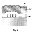
- FIG. 1 to 5 show, respectively in section, the inventive manufacturing method in an embodiment, wherein FIG. 4 an enlarged detail from the FIG. 3 represents.
- FIG. 1 a manufacturing stage is shown in which already micromechanical structures 2, for example a comb structure for a rotation rate or acceleration sensor, are structured on a silicon substrate 1, but not yet by etching a sacrificial layer 3 located below the structures 2, preferably on an SiGe sacrificial layer basis. have been exposed.
- a sacrificial layer 3 located below the structures 2, preferably on an SiGe sacrificial layer basis.
- modifications with, for example, poly-Si sacrificial layers 3 are conceivable in which the structures 2 are to be exposed before the method steps described below.
- the sensor structures 2 are subsequently covered with a silicon-germanium (SiGe) filling layer 4. They are thus stationary up to the etching of the SiGe sacrificial layer 3 and therefore insensitive to mechanical shocks.
- the SiGe filling layer 4 is later removed highly selectively with respect to the silicon sensor structures 2 by means of ClF 3 etching and is thus also a sacrificial layer.
- the in FIG. 1 detectable (some 100nm to several microns thick) poly-Si layer 7 deposited. This is then, as in the further process steps according to FIGS. 2 to 5
- the SiGe of the filling layer 4 is preferably p-doped first.
- a thin germanium layer 5 with a thickness of a few 10-100 nm, also p-doped, cf. FIG. 1 .
- the SiGe filling layer 4 can be deposited with a Ge concentration gradient so that a Ge rich (partial) layer 5 results in its upper, substrate-distant region.
- an electrical contact 6 to the substrate 1 for the subsequent pore formation is required, cf. FIG. 1 ,
- This connection can also be made via the SiGe layer 4 or the poly-Si layer 7.
- the deposition of the already mentioned thick poly-Si layer 7, p-doped takes place. This represents the later cap 7.
- the poly-Si layer 7 and the Ge-rich layer 5 are partially porosified by means of electrochemical etching in hydrofluoric acid (HF), so that the in FIG. 2 shown state with the porous layers 9 and 10 results.
- HF hydrofluoric acid
- an etching mask 8, cf. FIG. 1 isolated and structured.
- layers 8 of SiN, Si 3 N 4 or n-type dopants are used here.
- stain-etch As an alternative to electrochemical etching, a per se known electroless etching process (so-called stain-etch) can also be used.
- the micropores are formed in a mixture of HF and an oxidizing agent (eg H 2 O 2 , HNO 3 ).
- an oxidizing agent eg H 2 O 2 , HNO 3 .
- FIG. 2 recognizable porous layers 9 and 10 thermally oxidized, so that the state according to Figure 3 results.
- This oxidation is preferably carried out at low temperatures by 200-400 ° C, so that no thermal influence of the SiGe filling layer 4 and the Ge-rich layer 5 takes place.
- the oxide of the Ge-rich layer 5 is not stable in contrast to the oxidized porous silicon 11 and can be dissolved, for example, in H 2 0 or H 2 O vapor.
- the oxidized porous silicon 11 now provides access holes for the C1F 3 etch process. Downwardly, access is ensured through the porous Ge-rich layer 10, the oxide film of which has been removed as described.
- the porous cap 7 or 11 is sealed by deposition of a thin sealing layer 13.
- the openings that is, micropores of this cap 7, are in the range of 2-20, in particular less than 5 nm in diameter and can therefore be closed with sufficient for a reliable closure sealing layers 13 with a thickness of 100nm, without the underlying sensor structure 12 coated becomes.
- a process vacuum or a defined process atmosphere may be included in the closure.
- an ASC Anti-Stiction Coating
- the method according to the invention is applicable to all silicon-based sensors which require a capping.
Claims (9)
- Procédé de fabrication d'un composant micromécanique avec une couche périphérique en silicium, comportant au moins les étapes suivantes :- dépôt d'une couche de charge en silicium/germanium (4) sur un substrat (1) et création d'une couche riche en germanium (5), cette dernière étant créée soit par un gradient de concentration de germanium croissant vers le haut de la couche de charge en silicium/germanium (4) ou par dépôt d'une couche de germanium (5) supplémentaire sur la couche de charge en silicium/germanium (4),- dépôt d'une couche périphérique de silicium (7) sur la couche riche en germanium (5),- ménagement dans la couche périphérique de silicium (7) et dans la couche riche en germanium (5) de micropores dont les diamètres sont de l'ordre de nanomètres, ce qui a pour effet de créer des couches poreuses (9, 10),- thermo-oxydation des couches poreuses (9, 10) et ensuite retrait de l'oxyde de la couche poreuse riche en germanium (10) par un processus de dissolution des oxydes,- retrait de la couche de charge en silicium/germanium (4) et de la couche riche en germanium (5, 10) par décapage en phase gazeuse par CIF3 amené à travers les micropores,- scellement des micropores par dépôt d'une couche d'obturation (13) sur la couche périphérique poreuse en silicium (11).
- Procédé selon la revendication 1, caractérisé en ce que la couche riche en germanium (5, 10) présente une épaisseur d'environ 30 à 100 nm.
- Procédé selon la revendication 1 ou 2, caractérisé en ce que la thermo-oxydation s'effectue à des températures d'environ 200 à 400 degrés Celsius.
- Procédé selon l'une quelconque des revendications 1 à 3, caractérisé en ce que l'oxyde de la couche riche en germanium (10) est dissous dans de l'eau ou de la vapeur d'eau.
- Procédé selon l'une quelconque des revendications 1 à 4, caractérisé en ce qu'avant le dépôt de la couche de charge en silicium/germanium (4), on applique sous les structures micromécaniques (2) devant être mises à nu une couche sacrificielle de silicium/germanium (3) et en ce qu'on élimine en une seule étape de décapage la couche sacrificielle de silicium/germanium et la couche de charge (3, 4) et on met à nu les structures (2, 12).
- Procédé selon l'une quelconque des revendications 1 à 4, caractérisé en ce que le dépôt de la couche de charge en silicium/germanium (4) s'effectue sur des structures micromécaniques (12) d'ores et déjà mises à nu à l'aide d'une couche sacrificielle non constituée de silicium/germanium.
- Procédé selon l'une quelconque des revendications 1 à 6, caractérisé en ce que le diamètre des micropores est de l'ordre de 2 à 20 nm.
- Procédé selon la revendication 7, caractérisé en ce que la couche d'obturation (13) présente une épaisseur de 100 nm.
- Procédé selon l'une quelconque des revendications 1 à 8, caractérisé en ce qu'on créé les micropores par décapage électrochimique ou par un processus de dissolution chimique (stain etching) sans courant électrique.
Applications Claiming Priority (2)
| Application Number | Priority Date | Filing Date | Title |
|---|---|---|---|
| DE102006049259A DE102006049259A1 (de) | 2006-10-19 | 2006-10-19 | Verfahren zur Herstellung eines mikromechanischen Bauelementes mit einer Dünnschicht-Verkappung |
| PCT/EP2007/058684 WO2008046682A1 (fr) | 2006-10-19 | 2007-08-21 | procédé de construction d'un composant micromécanique doté d'un recouvrement en couche mince |
Publications (2)
| Publication Number | Publication Date |
|---|---|
| EP2084102A1 EP2084102A1 (fr) | 2009-08-05 |
| EP2084102B1 true EP2084102B1 (fr) | 2011-10-26 |
Family
ID=38694872
Family Applications (1)
| Application Number | Title | Priority Date | Filing Date |
|---|---|---|---|
| EP07802761A Not-in-force EP2084102B1 (fr) | 2006-10-19 | 2007-08-21 | Procédé de construction d'un composant micromécanique doté d'un recrouvement en couche mince |
Country Status (7)
| Country | Link |
|---|---|
| US (1) | US7851248B2 (fr) |
| EP (1) | EP2084102B1 (fr) |
| JP (1) | JP2010506740A (fr) |
| CN (1) | CN101528589A (fr) |
| AT (1) | ATE530496T1 (fr) |
| DE (1) | DE102006049259A1 (fr) |
| WO (1) | WO2008046682A1 (fr) |
Families Citing this family (11)
| Publication number | Priority date | Publication date | Assignee | Title |
|---|---|---|---|---|
| DE102005047081B4 (de) * | 2005-09-30 | 2019-01-31 | Robert Bosch Gmbh | Verfahren zum plasmalosen Ätzen von Silizium mit dem Ätzgas ClF3 oder XeF2 |
| DE102007008380B4 (de) * | 2007-02-21 | 2017-05-11 | Robert Bosch Gmbh | Mikromechanisches Bauelement und Verfahren zur Herstellung eines mikromechanischen Bauelements |
| US7719752B2 (en) | 2007-05-11 | 2010-05-18 | Qualcomm Mems Technologies, Inc. | MEMS structures, methods of fabricating MEMS components on separate substrates and assembly of same |
| WO2009041948A1 (fr) * | 2007-09-28 | 2009-04-02 | Qualcomm Mems Technologies, Inc. | Structure sacrificielle à composants multiples |
| FR2925888A1 (fr) * | 2007-12-27 | 2009-07-03 | Commissariat Energie Atomique | Dispositif a structure pre-liberee |
| KR101298114B1 (ko) * | 2009-06-02 | 2013-08-20 | 한국과학기술원 | Mems 또는 mems 소자의 패키지 및 패키징 방법 |
| DE102009027898B4 (de) | 2009-07-21 | 2019-09-05 | Robert Bosch Gmbh | Herstellungsverfahren für ein mikromechanisches Bauelement |
| DE102009029184A1 (de) | 2009-09-03 | 2011-03-10 | Robert Bosch Gmbh | Herstellungsverfahren für ein verkapptes mikromechanisches Bauelement, entsprechendes mikromechanisches Bauelement und Kappe für ein mikromechanisches Bauelement |
| FR2957339B1 (fr) * | 2010-03-10 | 2012-03-16 | Commissariat Energie Atomique | Procede de fabrication d'un microsysteme electromecanique |
| FR3002219B1 (fr) * | 2013-02-19 | 2015-04-10 | Commissariat Energie Atomique | Procede de fabrication d'une structure micromecanique et/ou nanomecanique comportant une surface poreuse |
| US10716382B2 (en) | 2018-04-30 | 2020-07-21 | L'oreal | Hair dye pen |
Family Cites Families (10)
| Publication number | Priority date | Publication date | Assignee | Title |
|---|---|---|---|---|
| DE19961578A1 (de) | 1999-12-21 | 2001-06-28 | Bosch Gmbh Robert | Sensor mit zumindest einer mikromechanischen Struktur und Verfahren zur Herstellung |
| DE10006035A1 (de) | 2000-02-10 | 2001-08-16 | Bosch Gmbh Robert | Verfahren zur Herstellung eines mikromechanischen Bauelements sowie ein nach dem Verfahren hergestelltes Bauelement |
| US6998148B1 (en) * | 2001-03-28 | 2006-02-14 | Shipley Company, L.L.C. | Porous materials |
| JP2003224204A (ja) * | 2002-01-29 | 2003-08-08 | Mitsubishi Electric Corp | キャパシタを有する半導体装置 |
| US6936491B2 (en) * | 2003-06-04 | 2005-08-30 | Robert Bosch Gmbh | Method of fabricating microelectromechanical systems and devices having trench isolated contacts |
| US7075160B2 (en) | 2003-06-04 | 2006-07-11 | Robert Bosch Gmbh | Microelectromechanical systems and devices having thin film encapsulated mechanical structures |
| JP5009505B2 (ja) * | 2004-03-03 | 2012-08-22 | ローベルト ボツシユ ゲゼルシヤフト ミツト ベシユレンクテル ハフツング | ダイヤフラムを備えたマイクロマシニング型の構成エレメントおよびこのような構成エレメントを製作するための方法 |
| DE102004036803A1 (de) | 2004-07-29 | 2006-03-23 | Robert Bosch Gmbh | Verfahren zum Ätzen einer Schicht auf einem Substrat |
| DE102005004877A1 (de) * | 2005-02-03 | 2006-08-10 | Robert Bosch Gmbh | Mikromechanisches Bauelement und entsprechendes Herstellungsverfahren |
| WO2006081636A1 (fr) | 2005-02-04 | 2006-08-10 | Interuniversitair Microelektronica Centrum (Imec) | Procede d'encapsulation d'un dispositif dans une microcavite |
-
2006
- 2006-10-19 DE DE102006049259A patent/DE102006049259A1/de not_active Withdrawn
-
2007
- 2007-08-21 AT AT07802761T patent/ATE530496T1/de active
- 2007-08-21 JP JP2009532744A patent/JP2010506740A/ja not_active Withdrawn
- 2007-08-21 WO PCT/EP2007/058684 patent/WO2008046682A1/fr active Application Filing
- 2007-08-21 US US12/305,150 patent/US7851248B2/en not_active Expired - Fee Related
- 2007-08-21 CN CNA2007800389910A patent/CN101528589A/zh active Pending
- 2007-08-21 EP EP07802761A patent/EP2084102B1/fr not_active Not-in-force
Also Published As
| Publication number | Publication date |
|---|---|
| US7851248B2 (en) | 2010-12-14 |
| CN101528589A (zh) | 2009-09-09 |
| US20100003790A1 (en) | 2010-01-07 |
| ATE530496T1 (de) | 2011-11-15 |
| EP2084102A1 (fr) | 2009-08-05 |
| DE102006049259A1 (de) | 2008-04-30 |
| WO2008046682A1 (fr) | 2008-04-24 |
| JP2010506740A (ja) | 2010-03-04 |
Similar Documents
| Publication | Publication Date | Title |
|---|---|---|
| EP2084102B1 (fr) | Procédé de construction d'un composant micromécanique doté d'un recrouvement en couche mince | |
| EP1334060B1 (fr) | Composant micromecanique et procede de production correspondant | |
| EP2300356B1 (fr) | Procédé pour produire une structure membranaire micro-mécanique comportant un accès par le côté arrière du substrat | |
| EP1774572B1 (fr) | Procédé pour graver une couche sur un substrat | |
| DE10063991B4 (de) | Verfahren zur Herstellung von mikromechanischen Bauelementen | |
| EP1335878B1 (fr) | Composant a microstructure | |
| WO2001046066A2 (fr) | Capteur comportant au moins une structure micromecanique et procede de fabrication | |
| DE10030352A1 (de) | Mikromechanisches Bauelement, insbesondere Sensorelement, mit einer stabilisierten Membran und Verfahren zur Herstellung eines derartigen Bauelements | |
| DE102013209266A1 (de) | Bauelement mit einem Hohlraum | |
| DE102010061782B4 (de) | Verfahren zum Herstellen eines mikromechanischen Bauelements | |
| DE102009027898B4 (de) | Herstellungsverfahren für ein mikromechanisches Bauelement | |
| DE102016200499A1 (de) | Mikromechanisches Bauelement mit Diffusionsstoppkanal | |
| DE19913683C2 (de) | Verfahren zur Herstellung großflächiger Membranmasken | |
| EP1597193B1 (fr) | Procede de fabrication d'un composant comportant un support a semiconducteurs | |
| DE102017207111A1 (de) | Verfahren zum Herstellen eines mikromechanischen Inertialsensors | |
| EP1716070B1 (fr) | Detecteur micromecanique | |
| DE10046621A1 (de) | Verfahren zur Herstellung eines Membransensor-Arrays sowie Membransensor-Array | |
| DE10244785A1 (de) | Verfahren und mikromechanisches Bauelement | |
| DE102005005551B4 (de) | Mikromechanisches Bauelement mit einer Membran und Verfahren zur Herstellung eines solchen Bauelements | |
| DE102015224523A1 (de) | Zusätzliche Fläche zur Stabilisierung des Kaverneninnendrucks über Lebenszeit | |
| WO2020216776A1 (fr) | Composant micromécanique comprenant une membrane et une cavité, et procédé de fabrication associé | |
| DE102010038810A1 (de) | Verfahren zum Verkappen eines mikromechanischen Bauelements und mikromechanisches Bauelement | |
| WO2003052364A1 (fr) | Procede de production d'une microstructure | |
| DE102015224528A1 (de) | Anschläge als Getter zur Stabilisierung des Kaverneninnendruckes | |
| DE102004024285A1 (de) | Mikrostrukturiertes Bauelement und ein Verfahren zur Herstellung eines mikrostrukturierten Bauelements |
Legal Events
| Date | Code | Title | Description |
|---|---|---|---|
| PUAI | Public reference made under article 153(3) epc to a published international application that has entered the european phase |
Free format text: ORIGINAL CODE: 0009012 |
|
| 17P | Request for examination filed |
Effective date: 20090519 |
|
| AK | Designated contracting states |
Kind code of ref document: A1 Designated state(s): AT BE BG CH CY CZ DE DK EE ES FI FR GB GR HU IE IS IT LI LT LU LV MC MT NL PL PT RO SE SI SK TR |
|
| 17Q | First examination report despatched |
Effective date: 20091013 |
|
| DAX | Request for extension of the european patent (deleted) | ||
| GRAP | Despatch of communication of intention to grant a patent |
Free format text: ORIGINAL CODE: EPIDOSNIGR1 |
|
| GRAS | Grant fee paid |
Free format text: ORIGINAL CODE: EPIDOSNIGR3 |
|
| GRAA | (expected) grant |
Free format text: ORIGINAL CODE: 0009210 |
|
| AK | Designated contracting states |
Kind code of ref document: B1 Designated state(s): AT BE BG CH CY CZ DE DK EE ES FI FR GB GR HU IE IS IT LI LT LU LV MC MT NL PL PT RO SE SI SK TR |
|
| REG | Reference to a national code |
Ref country code: GB Ref legal event code: FG4D Free format text: NOT ENGLISH |
|
| REG | Reference to a national code |
Ref country code: CH Ref legal event code: EP |
|
| REG | Reference to a national code |
Ref country code: IE Ref legal event code: FG4D |
|
| REG | Reference to a national code |
Ref country code: DE Ref legal event code: R096 Ref document number: 502007008542 Country of ref document: DE Effective date: 20111222 |
|
| REG | Reference to a national code |
Ref country code: NL Ref legal event code: VDEP Effective date: 20111026 |
|
| LTIE | Lt: invalidation of european patent or patent extension |
Effective date: 20111026 |
|
| PG25 | Lapsed in a contracting state [announced via postgrant information from national office to epo] |
Ref country code: IS Free format text: LAPSE BECAUSE OF FAILURE TO SUBMIT A TRANSLATION OF THE DESCRIPTION OR TO PAY THE FEE WITHIN THE PRESCRIBED TIME-LIMIT Effective date: 20120226 Ref country code: LT Free format text: LAPSE BECAUSE OF FAILURE TO SUBMIT A TRANSLATION OF THE DESCRIPTION OR TO PAY THE FEE WITHIN THE PRESCRIBED TIME-LIMIT Effective date: 20111026 |
|
| PG25 | Lapsed in a contracting state [announced via postgrant information from national office to epo] |
Ref country code: SI Free format text: LAPSE BECAUSE OF FAILURE TO SUBMIT A TRANSLATION OF THE DESCRIPTION OR TO PAY THE FEE WITHIN THE PRESCRIBED TIME-LIMIT Effective date: 20111026 Ref country code: LV Free format text: LAPSE BECAUSE OF FAILURE TO SUBMIT A TRANSLATION OF THE DESCRIPTION OR TO PAY THE FEE WITHIN THE PRESCRIBED TIME-LIMIT Effective date: 20111026 Ref country code: SE Free format text: LAPSE BECAUSE OF FAILURE TO SUBMIT A TRANSLATION OF THE DESCRIPTION OR TO PAY THE FEE WITHIN THE PRESCRIBED TIME-LIMIT Effective date: 20111026 Ref country code: NL Free format text: LAPSE BECAUSE OF FAILURE TO SUBMIT A TRANSLATION OF THE DESCRIPTION OR TO PAY THE FEE WITHIN THE PRESCRIBED TIME-LIMIT Effective date: 20111026 Ref country code: PL Free format text: LAPSE BECAUSE OF FAILURE TO SUBMIT A TRANSLATION OF THE DESCRIPTION OR TO PAY THE FEE WITHIN THE PRESCRIBED TIME-LIMIT Effective date: 20111026 Ref country code: GR Free format text: LAPSE BECAUSE OF FAILURE TO SUBMIT A TRANSLATION OF THE DESCRIPTION OR TO PAY THE FEE WITHIN THE PRESCRIBED TIME-LIMIT Effective date: 20120127 Ref country code: PT Free format text: LAPSE BECAUSE OF FAILURE TO SUBMIT A TRANSLATION OF THE DESCRIPTION OR TO PAY THE FEE WITHIN THE PRESCRIBED TIME-LIMIT Effective date: 20120227 |
|
| REG | Reference to a national code |
Ref country code: IE Ref legal event code: FD4D |
|
| PG25 | Lapsed in a contracting state [announced via postgrant information from national office to epo] |
Ref country code: CY Free format text: LAPSE BECAUSE OF FAILURE TO SUBMIT A TRANSLATION OF THE DESCRIPTION OR TO PAY THE FEE WITHIN THE PRESCRIBED TIME-LIMIT Effective date: 20111026 |
|
| PG25 | Lapsed in a contracting state [announced via postgrant information from national office to epo] |
Ref country code: DK Free format text: LAPSE BECAUSE OF FAILURE TO SUBMIT A TRANSLATION OF THE DESCRIPTION OR TO PAY THE FEE WITHIN THE PRESCRIBED TIME-LIMIT Effective date: 20111026 Ref country code: CZ Free format text: LAPSE BECAUSE OF FAILURE TO SUBMIT A TRANSLATION OF THE DESCRIPTION OR TO PAY THE FEE WITHIN THE PRESCRIBED TIME-LIMIT Effective date: 20111026 Ref country code: SK Free format text: LAPSE BECAUSE OF FAILURE TO SUBMIT A TRANSLATION OF THE DESCRIPTION OR TO PAY THE FEE WITHIN THE PRESCRIBED TIME-LIMIT Effective date: 20111026 Ref country code: EE Free format text: LAPSE BECAUSE OF FAILURE TO SUBMIT A TRANSLATION OF THE DESCRIPTION OR TO PAY THE FEE WITHIN THE PRESCRIBED TIME-LIMIT Effective date: 20111026 Ref country code: BG Free format text: LAPSE BECAUSE OF FAILURE TO SUBMIT A TRANSLATION OF THE DESCRIPTION OR TO PAY THE FEE WITHIN THE PRESCRIBED TIME-LIMIT Effective date: 20120126 Ref country code: IE Free format text: LAPSE BECAUSE OF FAILURE TO SUBMIT A TRANSLATION OF THE DESCRIPTION OR TO PAY THE FEE WITHIN THE PRESCRIBED TIME-LIMIT Effective date: 20111026 |
|
| PG25 | Lapsed in a contracting state [announced via postgrant information from national office to epo] |
Ref country code: RO Free format text: LAPSE BECAUSE OF FAILURE TO SUBMIT A TRANSLATION OF THE DESCRIPTION OR TO PAY THE FEE WITHIN THE PRESCRIBED TIME-LIMIT Effective date: 20111026 |
|
| PLBE | No opposition filed within time limit |
Free format text: ORIGINAL CODE: 0009261 |
|
| STAA | Information on the status of an ep patent application or granted ep patent |
Free format text: STATUS: NO OPPOSITION FILED WITHIN TIME LIMIT |
|
| 26N | No opposition filed |
Effective date: 20120727 |
|
| REG | Reference to a national code |
Ref country code: DE Ref legal event code: R097 Ref document number: 502007008542 Country of ref document: DE Effective date: 20120727 |
|
| BERE | Be: lapsed |
Owner name: ROBERT BOSCH G.M.B.H. Effective date: 20120831 |
|
| REG | Reference to a national code |
Ref country code: CH Ref legal event code: PL |
|
| PG25 | Lapsed in a contracting state [announced via postgrant information from national office to epo] |
Ref country code: MC Free format text: LAPSE BECAUSE OF NON-PAYMENT OF DUE FEES Effective date: 20120831 |
|
| PG25 | Lapsed in a contracting state [announced via postgrant information from national office to epo] |
Ref country code: ES Free format text: LAPSE BECAUSE OF FAILURE TO SUBMIT A TRANSLATION OF THE DESCRIPTION OR TO PAY THE FEE WITHIN THE PRESCRIBED TIME-LIMIT Effective date: 20120206 Ref country code: LI Free format text: LAPSE BECAUSE OF NON-PAYMENT OF DUE FEES Effective date: 20120831 Ref country code: CH Free format text: LAPSE BECAUSE OF NON-PAYMENT OF DUE FEES Effective date: 20120831 |
|
| PG25 | Lapsed in a contracting state [announced via postgrant information from national office to epo] |
Ref country code: BE Free format text: LAPSE BECAUSE OF NON-PAYMENT OF DUE FEES Effective date: 20120831 |
|
| PG25 | Lapsed in a contracting state [announced via postgrant information from national office to epo] |
Ref country code: FI Free format text: LAPSE BECAUSE OF FAILURE TO SUBMIT A TRANSLATION OF THE DESCRIPTION OR TO PAY THE FEE WITHIN THE PRESCRIBED TIME-LIMIT Effective date: 20111026 |
|
| REG | Reference to a national code |
Ref country code: AT Ref legal event code: MM01 Ref document number: 530496 Country of ref document: AT Kind code of ref document: T Effective date: 20120831 |
|
| PG25 | Lapsed in a contracting state [announced via postgrant information from national office to epo] |
Ref country code: AT Free format text: LAPSE BECAUSE OF NON-PAYMENT OF DUE FEES Effective date: 20120831 |
|
| PG25 | Lapsed in a contracting state [announced via postgrant information from national office to epo] |
Ref country code: MT Free format text: LAPSE BECAUSE OF FAILURE TO SUBMIT A TRANSLATION OF THE DESCRIPTION OR TO PAY THE FEE WITHIN THE PRESCRIBED TIME-LIMIT Effective date: 20111026 |
|
| PG25 | Lapsed in a contracting state [announced via postgrant information from national office to epo] |
Ref country code: TR Free format text: LAPSE BECAUSE OF FAILURE TO SUBMIT A TRANSLATION OF THE DESCRIPTION OR TO PAY THE FEE WITHIN THE PRESCRIBED TIME-LIMIT Effective date: 20111026 |
|
| PG25 | Lapsed in a contracting state [announced via postgrant information from national office to epo] |
Ref country code: LU Free format text: LAPSE BECAUSE OF NON-PAYMENT OF DUE FEES Effective date: 20120821 |
|
| PG25 | Lapsed in a contracting state [announced via postgrant information from national office to epo] |
Ref country code: HU Free format text: LAPSE BECAUSE OF FAILURE TO SUBMIT A TRANSLATION OF THE DESCRIPTION OR TO PAY THE FEE WITHIN THE PRESCRIBED TIME-LIMIT Effective date: 20070821 |
|
| REG | Reference to a national code |
Ref country code: FR Ref legal event code: PLFP Year of fee payment: 10 |
|
| PGFP | Annual fee paid to national office [announced via postgrant information from national office to epo] |
Ref country code: IT Payment date: 20160823 Year of fee payment: 10 Ref country code: GB Payment date: 20160824 Year of fee payment: 10 |
|
| PGFP | Annual fee paid to national office [announced via postgrant information from national office to epo] |
Ref country code: FR Payment date: 20160825 Year of fee payment: 10 |
|
| PGFP | Annual fee paid to national office [announced via postgrant information from national office to epo] |
Ref country code: DE Payment date: 20171026 Year of fee payment: 11 |
|
| GBPC | Gb: european patent ceased through non-payment of renewal fee |
Effective date: 20170821 |
|
| REG | Reference to a national code |
Ref country code: FR Ref legal event code: ST Effective date: 20180430 |
|
| PG25 | Lapsed in a contracting state [announced via postgrant information from national office to epo] |
Ref country code: GB Free format text: LAPSE BECAUSE OF NON-PAYMENT OF DUE FEES Effective date: 20170821 |
|
| PG25 | Lapsed in a contracting state [announced via postgrant information from national office to epo] |
Ref country code: FR Free format text: LAPSE BECAUSE OF NON-PAYMENT OF DUE FEES Effective date: 20170831 Ref country code: IT Free format text: LAPSE BECAUSE OF NON-PAYMENT OF DUE FEES Effective date: 20170821 |
|
| REG | Reference to a national code |
Ref country code: DE Ref legal event code: R119 Ref document number: 502007008542 Country of ref document: DE |
|
| PG25 | Lapsed in a contracting state [announced via postgrant information from national office to epo] |
Ref country code: DE Free format text: LAPSE BECAUSE OF NON-PAYMENT OF DUE FEES Effective date: 20190301 |