EP1597193B1 - Procede de fabrication d'un composant comportant un support a semiconducteurs - Google Patents
Procede de fabrication d'un composant comportant un support a semiconducteurs Download PDFInfo
- Publication number
- EP1597193B1 EP1597193B1 EP03782094.1A EP03782094A EP1597193B1 EP 1597193 B1 EP1597193 B1 EP 1597193B1 EP 03782094 A EP03782094 A EP 03782094A EP 1597193 B1 EP1597193 B1 EP 1597193B1
- Authority
- EP
- European Patent Office
- Prior art keywords
- silicon
- porous
- depressions
- region
- depression
- Prior art date
- Legal status (The legal status is an assumption and is not a legal conclusion. Google has not performed a legal analysis and makes no representation as to the accuracy of the status listed.)
- Expired - Lifetime
Links
- 238000000034 method Methods 0.000 title claims description 33
- 239000004065 semiconductor Substances 0.000 title claims description 19
- 238000004519 manufacturing process Methods 0.000 title claims description 18
- 239000000463 material Substances 0.000 claims description 16
- 230000000873 masking effect Effects 0.000 claims description 10
- 230000015572 biosynthetic process Effects 0.000 claims description 6
- 229910021426 porous silicon Inorganic materials 0.000 description 31
- 229910052710 silicon Inorganic materials 0.000 description 30
- XUIMIQQOPSSXEZ-UHFFFAOYSA-N Silicon Chemical compound [Si] XUIMIQQOPSSXEZ-UHFFFAOYSA-N 0.000 description 29
- 239000010703 silicon Substances 0.000 description 29
- 238000005530 etching Methods 0.000 description 15
- 239000011148 porous material Substances 0.000 description 13
- 238000005229 chemical vapour deposition Methods 0.000 description 9
- KRHYYFGTRYWZRS-UHFFFAOYSA-N Fluorane Chemical compound F KRHYYFGTRYWZRS-UHFFFAOYSA-N 0.000 description 8
- 239000000758 substrate Substances 0.000 description 8
- 235000012431 wafers Nutrition 0.000 description 6
- 238000002955 isolation Methods 0.000 description 4
- 230000003647 oxidation Effects 0.000 description 4
- 238000007254 oxidation reaction Methods 0.000 description 4
- 230000000694 effects Effects 0.000 description 3
- 238000009413 insulation Methods 0.000 description 3
- 239000000126 substance Substances 0.000 description 3
- LFQSCWFLJHTTHZ-UHFFFAOYSA-N Ethanol Chemical compound CCO LFQSCWFLJHTTHZ-UHFFFAOYSA-N 0.000 description 2
- 240000006829 Ficus sundaica Species 0.000 description 2
- VYPSYNLAJGMNEJ-UHFFFAOYSA-N Silicium dioxide Chemical group O=[Si]=O VYPSYNLAJGMNEJ-UHFFFAOYSA-N 0.000 description 2
- 239000013590 bulk material Substances 0.000 description 2
- 239000013078 crystal Substances 0.000 description 2
- 239000003792 electrolyte Substances 0.000 description 2
- 239000007789 gas Substances 0.000 description 2
- 239000012528 membrane Substances 0.000 description 2
- MYMOFIZGZYHOMD-UHFFFAOYSA-N Dioxygen Chemical compound O=O MYMOFIZGZYHOMD-UHFFFAOYSA-N 0.000 description 1
- 238000004458 analytical method Methods 0.000 description 1
- 238000007743 anodising Methods 0.000 description 1
- 238000010276 construction Methods 0.000 description 1
- 238000000708 deep reactive-ion etching Methods 0.000 description 1
- 230000001419 dependent effect Effects 0.000 description 1
- 238000000151 deposition Methods 0.000 description 1
- 230000008021 deposition Effects 0.000 description 1
- 238000009792 diffusion process Methods 0.000 description 1
- 230000005684 electric field Effects 0.000 description 1
- 238000003487 electrochemical reaction Methods 0.000 description 1
- 238000005516 engineering process Methods 0.000 description 1
- 230000017525 heat dissipation Effects 0.000 description 1
- 238000010438 heat treatment Methods 0.000 description 1
- 238000005468 ion implantation Methods 0.000 description 1
- 239000000203 mixture Substances 0.000 description 1
- 238000005457 optimization Methods 0.000 description 1
- 229920002120 photoresistant polymer Polymers 0.000 description 1
- 230000000704 physical effect Effects 0.000 description 1
- 238000004886 process control Methods 0.000 description 1
- 230000000717 retained effect Effects 0.000 description 1
- 238000007789 sealing Methods 0.000 description 1
- 229910052814 silicon oxide Inorganic materials 0.000 description 1
- 125000006850 spacer group Chemical group 0.000 description 1
- 230000006641 stabilisation Effects 0.000 description 1
- 238000011105 stabilization Methods 0.000 description 1
- 239000010409 thin film Substances 0.000 description 1
Images

Classifications
-
- B—PERFORMING OPERATIONS; TRANSPORTING
- B81—MICROSTRUCTURAL TECHNOLOGY
- B81C—PROCESSES OR APPARATUS SPECIALLY ADAPTED FOR THE MANUFACTURE OR TREATMENT OF MICROSTRUCTURAL DEVICES OR SYSTEMS
- B81C1/00—Manufacture or treatment of devices or systems in or on a substrate
- B81C1/00642—Manufacture or treatment of devices or systems in or on a substrate for improving the physical properties of a device
- B81C1/0069—Thermal properties, e.g. improve thermal insulation
-
- B—PERFORMING OPERATIONS; TRANSPORTING
- B81—MICROSTRUCTURAL TECHNOLOGY
- B81C—PROCESSES OR APPARATUS SPECIALLY ADAPTED FOR THE MANUFACTURE OR TREATMENT OF MICROSTRUCTURAL DEVICES OR SYSTEMS
- B81C2201/00—Manufacture or treatment of microstructural devices or systems
- B81C2201/01—Manufacture or treatment of microstructural devices or systems in or on a substrate
- B81C2201/0101—Shaping material; Structuring the bulk substrate or layers on the substrate; Film patterning
- B81C2201/0111—Bulk micromachining
- B81C2201/0115—Porous silicon
Definitions
- the invention relates to a method for producing a component with a semiconductor carrier.
- BMM bulk micro-mechanics
- a comparatively thick and poorly heat-conducting (0.3 to 1 W / mK) porous silicon layer is produced, which in addition can also be oxidized.
- Such layers are e.g. used for thermal decoupling of sensor or actuator structures in thermal components, such as thermal, chemical, fluidic sensors or gas sensors.
- German patent application DE 100 58 009 A1 is a flow sensor, in particular for the analysis of gas flows known, which has a support body and at least one sensitive to a flow of a medium sensor component.
- the sensor component is at least partially separated from the support body by a porous silicon region or a porous silicon oxide region.
- a microwave electric element in which a structure of porous silicon is formed on a silicon substrate to form the electrical element.
- the structure is generated by means of thermal oxidation.
- a micromechanical air mass sensor in which a thin film resistor is arranged above the opening for the air flow on a silicon substrate.
- an infrared-based microbolometer that has a bridge of porous silicon.
- the manufacturing step that recesses are closed with a cover layer is not disclosed.
- a transistor-semiconductor structure in which a lower and an upper silicon pattern structure are separated by an insulating layer.
- a channel region of porous silicon is provided. It is also shown a corresponding manufacturing method.
- porous semiconductors for example porous silicon
- an electrochemical reaction between hydrofluoric acid and silicon is generally used, in which a sponge-like structure is produced in the silicon.
- the silicon semiconductor carrier generally a silicon wafer
- the resulting porous structure gives the silicon a large internal surface and other chemical and physical properties (eg lower thermal conductivity) than the surrounding bulk silicon.
- etching silicon For etching silicon are holes (holes) necessary at the interface between silicon and electrolyte provided by the flowing stream. If the Storm Density is less than a critical current density, holes diffuse through the applied electric field to recesses lying in the surface, in which a preferred etching takes place. For example, in p-doped silicon, the areas between the pits are laterally etched to a minimum thickness until quantum effects prevent holes from entering those areas and stop the etch. In this way, a spongy skeleton structure of silicon and etched pores is created. Since during the formation of the skeleton structure the etching takes place only in the region of the pore tips, the sponge structure of already etched silicon is retained. Thus, the pore size in the already etched areas remains almost unchanged.
- the pore size is dependent on the HF concentration in the hydrofluoric acid, the doping and the current density, and may be from a few nm to a few ⁇ m . Likewise, the porosity is adjustable in a range of about 10% to more than 90%.
- porous silicon For the production of porous silicon differently doped substrates can be used. Typically, p-type wafers with different doping levels are used. By doping, the structure within the porous silicon can be determined.
- p- and n-doped silicon have a very different etching behavior. Under the conditions in which porous silicon can be produced in p-doped silicon, is this is not possible in n-doped silicon or only to a very limited extent.
- a layer on the surface of the p-doped substrate can be n-umdotiert (eg by ion implantation or diffusion).
- the porous silicon is regularly produced locally on a silicon substrate in thicknesses of several ⁇ m to several 100 ⁇ m .
- the porous silicon can be stabilized in its structure and its thermal conductivity depending on the porosity and crystal size can be further reduced.
- the result is oxidized porous silicon.
- the oxidized porous silicon is sealed with a cover layer, eg of CVD materials such as Si x N y (CVD stands for Chemical Vapor Depostion).
- CVD chemical Vapor Depostion
- trenches of several ⁇ m to several 100 ⁇ m are etched into the silicon by a deep-etching so that the silicon lattice, spacer webs or free-standing silicon pillars are formed. These are completely or only partially oxidized to reduce their thermal conductivity.
- the trenches are periodically closed by a CVD layer and the surface is planarized, if necessary, to deposit the active and sensitive elements.
- the invention is defined in claim 1 and starts first with a method for producing the component with a semiconductor carrier, in which porous semiconductor material is produced for the formation of at least one thermally decoupled structure.
- the essence of the invention resides in the fact that, in the porous material, one or more depressions are etched or etched in order to produce at least one thermally decoupled region defined by the one depression or the plurality of depressions and that above the at least one depression Area at least one structure is expanded.
- Porous semiconductors can be made through appropriate depressions, e.g. Create trenches, web structures, matrix-like columns on the surface of which the thermally decoupled structures can be applied.
- Stabilization and, if appropriate, further reduction of the vertical conductivity (that is to say perpendicular to a semiconductor carrier) of the porosized material regions can be achieved by virtue of the fact that the produced, porous semiconductor material is formed after the introduction of the depressions, e.g. Trenches, at least partially oxidized.
- oxidation of porous semiconductor material can also take place prior to the etching of depressions.
- the one or more depressions are etched only so deeply over a thickness of the porosized material that a desired lateral thermal decoupling is taking place. It has been found that a large part of the heat already flows off in the first 5 to 30 ⁇ m depth of the structures, so that it may be sufficient for a desired thermal functionality, the porous material only over a corresponding part of the thickness, eg 50 ⁇ m, structure. Depending on the produced thickness of the porous material can thus remain residual thickness of porous material.
- hard or resist masks can be used for the production of locally limited porous semiconductor material.
- Hard masks can usually remain in the layer structure, since the structures of porous material be regularly closed with an insulating cover layer before building other structures.
- the masking In order to further improve the lateral thermal decoupling, it is furthermore advantageous if, in particular in the case in which the masking remains in the layer structure, it is undercut in the structuring of the porosified regions by etching depressions. Due to the remaining masking, therefore, although the larger lateral distances between the porosized regions no larger lateral gaps must be closed by the cover layer, because the opening width is determined by the mask.
- a further improvement in the thermal decoupling can be achieved in that the at least one region of porous material defined in the foot region by the one depression and / or several depressions is isotropically undercut.
- This procedure can be used in particular preferably when the porosate material is completely etched through with respect to the one or more depressions, so that there is nonporous bulk semiconductor material in the foot region, which etches with high selectivity, in particular to form an oxidized, porous structure leaves.
- the essential aspect of the device according to the invention is in that the at least one porous area to the surrounding material in the lateral direction is at least partially separated by a cavity that is many times larger than the pores of the porosated area.
- this makes it possible to combine the good insulation properties of a trench structure in a lateral direction by an improved vertical isolation due to porous material, whereby the good mechanical stability of such a structure can still be used in particular.
- the structure is particularly advantageous when there are several porosity regions which are separated at least in one direction by cavities.
- the device has a plurality of pillars which are porosiert at least over part of their height.
- a web structure i. a structure that has a lateral connection to the bulk material on opposite sides.
- An optimization with regard to a lateral isolation of one or more porosized regions can be achieved in that the cavity in the lateral direction extends completely around the one or more porous regions.
- the column structure already mentioned above may be mentioned.
- a component can be further improved if the cavity in particular also extends below the one or more porous regions.
- a column or web structure can be realized in which the columns or webs "hang freely”.
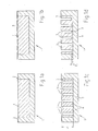
- Fig. 1a to 1c each show a schematic sectional view of the formation of a thermal component based on a silicon wafer 1.
- a first step locally porous silicon 3 is first produced by means of a mask 2 (see FIG. Fig. 1a ).
- the trenches 6, e.g. closed by a CVD (Chemical Vapor Deposition) layer e.g. closed by a CVD (Chemical Vapor Deposition) layer.
- the layer thickness necessary for closing essentially depends on the trench width b of the trenches 5.
- a large trench width b is advantageous for a good lateral insulation, but in view of the necessary thickness of a cover layer 7 (s. Fig. 4 ) of disadvantage.
- the minimum necessary layer thickness for sealing is determined by the width b CVD of the mask opening of the hard mask 8.
- the degree of undercutting can be determined to be very large, resulting in webs 6 with low heat dissipation in the depth and wide trenches, which ensure a nearly complete lateral isolation.
- the effective porosity of the structure is increased in this way.
- the thermal decoupling can be improved even further by an isotropic etching process, for example with XeF 2 or ClF 3 .
- the high selectivity of the etching process to the oxide-enclosed porous silicon crystals is utilized, which allows a preferred etching of the bulk silicon 9 under the porous silicon 3 (or the porous webs or columns 6). It creates a structure according to Fig. 3 with freely hanging webs or pillars 6. For reasons of stability, only a laterally anchored pillar or web structure is suitable, since the pillars or webs hang freely.
- the depressions formed in the porous silicon or oxidized porous silicon are regularly closed with a cover layer 7 (see Fig. 4 ).
- the cover layer may be a CVD cover layer, for example a silicon oxide layer.
- Fig. 4 is the in Fig. 1d illustrated manufacturing state shown with cover layer 7.
- the cover layer can still be planarized.
- the structures to be thermally decoupled are preferably deposited over the remaining porous structures, i. especially the columns or bars applied.
- the components to be thermally decoupled may be active or sensitive elements, such as heaters, measuring resistors or thermocouples.
- heaters and measuring resistors are preferably applied completely over the porous areas.
Landscapes
- Engineering & Computer Science (AREA)
- Physics & Mathematics (AREA)
- Thermal Sciences (AREA)
- Manufacturing & Machinery (AREA)
- Microelectronics & Electronic Packaging (AREA)
- Micromachines (AREA)
- Weting (AREA)
- Element Separation (AREA)
Claims (7)
- Procédé pour la fabrication d'un composant avec un support à semi-conducteurs (1), dans lequel, pour la formation d'au moins une structure de capteur ou d'acteur découplée thermiquement,- du matériau semi-conducteur poreux (3) est produit,- une cavité ou plusieurs cavités (5) sont gravées dans le matériau rendu poreux (3) afin de produire au moins une zone (6) découplée thermiquement définie par cette une cavité ou ces plusieurs cavités,- cette une cavité ou ces plusieurs cavités sont fermées avec une couche de recouvrement (7), et- ensuite, cette au moins une structure est formée au-dessus de cette au moins une zone (6) .
- Procédé selon la revendication 1, caractérisé en ce que le matériau semi-conducteur rendu poreux est au moins partiellement oxydé après la suite de la structuration.
- Procédé selon la revendication 1, caractérisé en ce que le matériau semi-conducteur rendu poreux est au moins partiellement oxydé avant la suite de la structuration.
- Procédé selon l'une des revendications précédentes, caractérisé en ce que cette une cavité ou ces plusieurs cavités (5) sont gravées sur une épaisseur d du matériau rendu poreux (3) de sorte qu'un découplage thermique latéral souhaité ait lieu.
- Procédé selon l'une des revendications précédentes, caractérisé en ce que l'on utilise des masques durs ou en vernis (4, 8) pour la fabrication de cette au moins une cavité.
- Procédé selon la revendication 5, caractérisé en ce que cette au moins une zone (6), laquelle est définie par cette une cavité ou ces plusieurs cavités (5), est soumise à une gravure sous-jacente sous le masquage (8).
- Procédé selon l'une des revendications précédentes, caractérisé en ce que cette au moins une zone (6) en matériau rendu poreux définie par cette une cavité ou ces plusieurs cavités (5) est soumise à une gravure sous-jacente isotrope dans la zone du pied.
Applications Claiming Priority (3)
| Application Number | Priority Date | Filing Date | Title |
|---|---|---|---|
| DE10306129A DE10306129A1 (de) | 2003-02-14 | 2003-02-14 | Verfahren zur Herstellung eines Bauelementes mit einem Halbleiterträger sowie Bauelement |
| DE10306129 | 2003-02-14 | ||
| PCT/DE2003/003688 WO2004071944A1 (fr) | 2003-02-14 | 2003-11-06 | Procede de fabrication d'un composant comportant un support a semiconducteurs et composant |
Publications (2)
| Publication Number | Publication Date |
|---|---|
| EP1597193A1 EP1597193A1 (fr) | 2005-11-23 |
| EP1597193B1 true EP1597193B1 (fr) | 2015-02-25 |
Family
ID=32747821
Family Applications (1)
| Application Number | Title | Priority Date | Filing Date |
|---|---|---|---|
| EP03782094.1A Expired - Lifetime EP1597193B1 (fr) | 2003-02-14 | 2003-11-06 | Procede de fabrication d'un composant comportant un support a semiconducteurs |
Country Status (4)
| Country | Link |
|---|---|
| US (1) | US7803646B2 (fr) |
| EP (1) | EP1597193B1 (fr) |
| DE (1) | DE10306129A1 (fr) |
| WO (1) | WO2004071944A1 (fr) |
Families Citing this family (7)
| Publication number | Priority date | Publication date | Assignee | Title |
|---|---|---|---|---|
| JP2009076694A (ja) * | 2007-09-20 | 2009-04-09 | Panasonic Corp | 窒化物半導体装置およびその製造方法 |
| US7777295B2 (en) * | 2007-12-11 | 2010-08-17 | Hvvi Semiconductors, Inc. | Semiconductor structure and method of manufacture |
| US7811896B2 (en) * | 2007-12-11 | 2010-10-12 | Hvvi Semiconductors, Inc. | Semiconductor structure and method of manufacture |
| DE102012210936A1 (de) | 2012-06-27 | 2014-01-02 | Robert Bosch Gmbh | Vorrichtung zur Erfassung mindestens einer Strömungseigenschaft eines fluiden Mediums |
| DE102013210512B4 (de) * | 2013-06-06 | 2016-01-07 | Robert Bosch Gmbh | Sensor mit Membran und Herstellungsverfahren |
| KR102043806B1 (ko) | 2014-10-17 | 2019-11-12 | 테크놀로지안 투트키무스케스쿠스 브이티티 오와이 | 슈퍼커패시터 본체로서의 사용에 적합한 블랭크, 슈퍼커패시터 및 다공성 실리콘 볼륨의 제조방법 |
| US9957159B2 (en) * | 2016-03-28 | 2018-05-01 | Evigia Systems, Inc. | System and method for an ovenized silicon platform using Si/SiO2 hybrid supports |
Citations (1)
| Publication number | Priority date | Publication date | Assignee | Title |
|---|---|---|---|---|
| US6359276B1 (en) * | 1998-10-21 | 2002-03-19 | Xiang Zheng Tu | Microbolom infrared sensors |
Family Cites Families (5)
| Publication number | Priority date | Publication date | Assignee | Title |
|---|---|---|---|---|
| US5231878A (en) * | 1991-12-23 | 1993-08-03 | Ford Motor Company | Mass air flow sensor |
| KR100304713B1 (ko) * | 1999-10-12 | 2001-11-02 | 윤종용 | 부분적인 soi 구조를 갖는 반도체소자 및 그 제조방법 |
| KR100331226B1 (ko) * | 2000-02-23 | 2002-04-26 | 이상헌 | 다공성 산화 실리콘 기둥을 이용하여 형성한 초고주파용 소자 |
| DE10058009A1 (de) | 2000-11-23 | 2002-06-06 | Bosch Gmbh Robert | Strömungssensor |
| DE10117486A1 (de) * | 2001-04-07 | 2002-10-17 | Bosch Gmbh Robert | Verfahren zur Herstelung eines Halbleiterbauelements sowie ein nach dem Verfahren hergestelltes Halbleiterbauelement |
-
2003
- 2003-02-14 DE DE10306129A patent/DE10306129A1/de not_active Withdrawn
- 2003-11-06 EP EP03782094.1A patent/EP1597193B1/fr not_active Expired - Lifetime
- 2003-11-06 US US10/544,821 patent/US7803646B2/en not_active Expired - Fee Related
- 2003-11-06 WO PCT/DE2003/003688 patent/WO2004071944A1/fr not_active Application Discontinuation
Patent Citations (1)
| Publication number | Priority date | Publication date | Assignee | Title |
|---|---|---|---|---|
| US6359276B1 (en) * | 1998-10-21 | 2002-03-19 | Xiang Zheng Tu | Microbolom infrared sensors |
Also Published As
| Publication number | Publication date |
|---|---|
| EP1597193A1 (fr) | 2005-11-23 |
| US20060258037A1 (en) | 2006-11-16 |
| US7803646B2 (en) | 2010-09-28 |
| DE10306129A1 (de) | 2004-08-26 |
| WO2004071944A1 (fr) | 2004-08-26 |
Similar Documents
| Publication | Publication Date | Title |
|---|---|---|
| DE10063991B4 (de) | Verfahren zur Herstellung von mikromechanischen Bauelementen | |
| EP1810947B1 (fr) | Dispositif semi-conducteur et son procédé de fabrication | |
| DE10030352A1 (de) | Mikromechanisches Bauelement, insbesondere Sensorelement, mit einer stabilisierten Membran und Verfahren zur Herstellung eines derartigen Bauelements | |
| EP1345842B1 (fr) | Procédé de production d'un composant semi-conducteur et composant semi-conducteur produit selon ce procédé et ayant notamment une masse mobile | |
| DE10352001A1 (de) | Mikromechanisches Bauelement mit einer Membran und Verfahren zur Herstellung eines solchen Bauelements | |
| EP2084102B1 (fr) | Procédé de construction d'un composant micromécanique doté d'un recrouvement en couche mince | |
| DE19843984B4 (de) | Verfahren zur Herstellung von Strahlungssensoren | |
| EP1379463B1 (fr) | Procédé pour produire un composant à semi-conducteur et composant à semi-conducteur obtenu selon le procédé | |
| EP1597193B1 (fr) | Procede de fabrication d'un composant comportant un support a semiconducteurs | |
| DE102005023699B4 (de) | Verfahren zur Herstellung eines mikromechanischen Bauelements mit einer Membran | |
| EP1340052A1 (fr) | Capteur d'ecoulement | |
| DE4310205C1 (de) | Verfahren zur Herstellung einer Lochstruktur in einem Substrat aus Silizium | |
| DE10046621B4 (de) | Verfahren zur Herstellung eines Membransensor-Arrays sowie Membransensor-Array | |
| DE10046622B4 (de) | Verfahren zur Herstellung einer Membransensoreinheit sowie Membransensoreinheit | |
| EP1306348B1 (fr) | Procédé de fabrication d'une unité capteuse à mémbrane et unité capteuse à mémbrane | |
| EP3790839B1 (fr) | Procédé destiné à fabriquer une unité de séquençage destinée à séquencer un matériau biochimique | |
| EP1966076A1 (fr) | Procede de fabrication d'une membrane sur un substrat semi-conducteur et element de construction micromecanique comprenant une telle membrane | |
| EP2217526B1 (fr) | Procédé pour produire des structures micromécaniques comportant des parois latérales en relief et un angle d'inclinaison variable | |
| DE102004024285B4 (de) | Verfahren zur Herstellung eines mikrostrukturierten Bauelements | |
| EP1306349B1 (fr) | Procédé de fabrication d'une série de capteurs à membrane et série de capteurs à membrane | |
| DE102005009422B4 (de) | Mikromechanisches Bauelement und entsprechendes Herstellungsverfahren | |
| WO2004028956A2 (fr) | Procede et composant micromecanique | |
| DE10219248A1 (de) | Mikromechanisches Bauelement mit thermisch isolierter Sensoreinrichtung und entsprechendes Herstellungsverfahren | |
| DE10117363A1 (de) | Verfahren zum Herstellen einer porösen Si0¶2¶-Scheibe |
Legal Events
| Date | Code | Title | Description |
|---|---|---|---|
| PUAI | Public reference made under article 153(3) epc to a published international application that has entered the european phase |
Free format text: ORIGINAL CODE: 0009012 |
|
| 17P | Request for examination filed |
Effective date: 20050914 |
|
| AK | Designated contracting states |
Kind code of ref document: A1 Designated state(s): AT BE BG CH CY CZ DE DK EE ES FI FR GB GR HU IE IT LI LU MC NL PT RO SE SI SK TR |
|
| RBV | Designated contracting states (corrected) |
Designated state(s): DE FR GB NL |
|
| 17Q | First examination report despatched |
Effective date: 20051118 |
|
| GRAP | Despatch of communication of intention to grant a patent |
Free format text: ORIGINAL CODE: EPIDOSNIGR1 |
|
| INTG | Intention to grant announced |
Effective date: 20141002 |
|
| GRAS | Grant fee paid |
Free format text: ORIGINAL CODE: EPIDOSNIGR3 |
|
| GRAA | (expected) grant |
Free format text: ORIGINAL CODE: 0009210 |
|
| AK | Designated contracting states |
Kind code of ref document: B1 Designated state(s): DE FR GB NL |
|
| REG | Reference to a national code |
Ref country code: GB Ref legal event code: FG4D Free format text: NOT ENGLISH |
|
| REG | Reference to a national code |
Ref country code: DE Ref legal event code: R096 Ref document number: 50315214 Country of ref document: DE Effective date: 20150409 |
|
| REG | Reference to a national code |
Ref country code: NL Ref legal event code: VDEP Effective date: 20150225 |
|
| PG25 | Lapsed in a contracting state [announced via postgrant information from national office to epo] |
Ref country code: NL Free format text: LAPSE BECAUSE OF FAILURE TO SUBMIT A TRANSLATION OF THE DESCRIPTION OR TO PAY THE FEE WITHIN THE PRESCRIBED TIME-LIMIT Effective date: 20150225 |
|
| REG | Reference to a national code |
Ref country code: FR Ref legal event code: PLFP Year of fee payment: 13 |
|
| REG | Reference to a national code |
Ref country code: DE Ref legal event code: R097 Ref document number: 50315214 Country of ref document: DE |
|
| PLBE | No opposition filed within time limit |
Free format text: ORIGINAL CODE: 0009261 |
|
| STAA | Information on the status of an ep patent application or granted ep patent |
Free format text: STATUS: NO OPPOSITION FILED WITHIN TIME LIMIT |
|
| 26N | No opposition filed |
Effective date: 20151126 |
|
| GBPC | Gb: european patent ceased through non-payment of renewal fee |
Effective date: 20151106 |
|
| PG25 | Lapsed in a contracting state [announced via postgrant information from national office to epo] |
Ref country code: GB Free format text: LAPSE BECAUSE OF NON-PAYMENT OF DUE FEES Effective date: 20151106 |
|
| REG | Reference to a national code |
Ref country code: FR Ref legal event code: PLFP Year of fee payment: 14 |
|
| REG | Reference to a national code |
Ref country code: FR Ref legal event code: PLFP Year of fee payment: 15 |
|
| PGFP | Annual fee paid to national office [announced via postgrant information from national office to epo] |
Ref country code: FR Payment date: 20191121 Year of fee payment: 17 |
|
| PGFP | Annual fee paid to national office [announced via postgrant information from national office to epo] |
Ref country code: DE Payment date: 20200124 Year of fee payment: 17 |
|
| REG | Reference to a national code |
Ref country code: DE Ref legal event code: R119 Ref document number: 50315214 Country of ref document: DE |
|
| PG25 | Lapsed in a contracting state [announced via postgrant information from national office to epo] |
Ref country code: FR Free format text: LAPSE BECAUSE OF NON-PAYMENT OF DUE FEES Effective date: 20201130 |
|
| PG25 | Lapsed in a contracting state [announced via postgrant information from national office to epo] |
Ref country code: DE Free format text: LAPSE BECAUSE OF NON-PAYMENT OF DUE FEES Effective date: 20210601 |