EP1331646A2 - Röntgenstrahlen reflektierende Spiegel mit verminderten thermischen Spannungen und Röntgenstrahloptische Systeme mit diesen Spiegeln - Google Patents
Röntgenstrahlen reflektierende Spiegel mit verminderten thermischen Spannungen und Röntgenstrahloptische Systeme mit diesen Spiegeln Download PDFInfo
- Publication number
- EP1331646A2 EP1331646A2 EP03001788A EP03001788A EP1331646A2 EP 1331646 A2 EP1331646 A2 EP 1331646A2 EP 03001788 A EP03001788 A EP 03001788A EP 03001788 A EP03001788 A EP 03001788A EP 1331646 A2 EP1331646 A2 EP 1331646A2
- Authority
- EP
- European Patent Office
- Prior art keywords
- mirror
- thermal
- ray
- transfer member
- reflective
- Prior art date
- Legal status (The legal status is an assumption and is not a legal conclusion. Google has not performed a legal analysis and makes no representation as to the accuracy of the status listed.)
- Withdrawn
Links
Images

Classifications
-
- G—PHYSICS
- G21—NUCLEAR PHYSICS; NUCLEAR ENGINEERING
- G21K—HANDLING OF PARTICLES OR IONISING RADIATION NOT OTHERWISE PROVIDED FOR; IRRADIATION DEVICES; GAMMA RAY OR X-RAY MICROSCOPES
- G21K1/00—Arrangements for handling particles or ionising radiation, e.g. focusing or moderating
- G21K1/06—Arrangements for handling particles or ionising radiation, e.g. focusing or moderating using diffraction, refraction or reflection, e.g. monochromators
Definitions
- This disclosure pertains to mirrors as used in X-ray reflective-optical systems, and to X-ray reflective-optical systems incorporating such mirrors.
- Such mirrors and optical systems are used, for example, in X-ray microlithography systems as used for manufacturing microelectronic devices such as semiconductor integrated circuits and display devices.
- Microlithography is a key technology used in the manufacture of microelectronic devices such as semiconductor integrated circuits and displays. Recent years have witnessed the progressive miniaturization of active circuit elements in microelectronic devices. In fact, this miniaturization has progressed to such an extent that conventional "optical” microlithography techniques (i.e ., microlithography performed using ultraviolet, or "UV", light) are increasingly incapable, due to diffraction limitations, of resolving individual active circuit elements used in such devices. As a result, substantial research and development effort currently is underway to develop a practical "next generation lithography” (NGL) technology capable of producing significantly finer pattern-element resolution than obtainable using optical microlithography, without a prohibitive reduction in throughput. The most promising avenue for achieving finer pattern-element resolution is utilization of a microlithography energy beam having a substantially shorter wavelength than the UV beam used for optical microlithography.
- NNL next generation lithography
- X-ray encompasses, in addition to the conventional X-ray wavelength range, the so-called “soft X-ray” (SXR) wavelengths, also termed “extreme ultraviolet” (EUV) wavelengths.
- SXR soft X-ray
- EUV extreme ultraviolet
- a typical X-ray projection-exposure (microlithography) system comprises an X-ray source, an illumination-optical system for the X-ray beam produced by the source, a reticle stage for holding a pattern-defining reticle, a projection-optical (image-formation) optical system, and a substrate stage for holding the lithographic substrate (e.g ., semiconductor wafer).
- a typical EUV source is a synchrotron-radiation source or a laser-plasma source.
- the illumination-optical system typically comprises one or more grazing-incidence reflective mirrors, one or more multilayer-coated reflective mirrors, and one or more filters that reflect or transmit X-ray radiation only of a prescribed wavelength.
- the illumination-optical system is situated and configured to illuminate a selected region of the reticle with an X-ray beam of a desired wavelength.
- the reticle typically is a reflective reticle rather than a transmissive reticle as used in optical microlithography.
- a transmissive reticle defines pattern elements as corresponding regions in a layer of X-ray-absorptive material formed on a thin, supporting layer of an X-ray-transmissive material.
- An X-ray-reflective reticle defines pattern elements as corresponding regions of a low-reflective layer formed on an X-ray-reflective multilayer coating.
- an image of the pattern defined by the reticle is transferred to the lithographic substrate by the projection-optical system.
- the substrate is coated with a material (termed a "resist") that chemically responds to the exposure.
- the projection-optical system typically comprises a plurality of multilayer-coated reflective mirrors. Since X-ray radiation is absorbed and attenuated by the atmosphere, the optical path from the X-ray source to the substrate is maintained at a suitable high vacuum.
- optical elements such as lenses and conventional reflective mirrors as used in optical microlithography cannot be used because no known substances exist that refract X-ray wavelengths. Also, the reflectivity of conventional substances to incident X-ray radiation typically is extremely low.
- optical systems for X-rays generally comprise grazing-incidence reflective mirrors (i.e ., mirrors that reflect, using total reflection, X-rays incident at an extremely high incidence angle to the reflective surface) and/or multilayer-coated reflective mirrors (i.e., mirrors that reflect X-rays incident at low angles of incidence by aligning the phases of X-rays reflected at respective interfaces of a multilayer coating formed on a polished surface of the mirror).
- grazing-incidence reflective mirrors i.e ., mirrors that reflect, using total reflection, X-rays incident at an extremely high incidence angle to the reflective surface
- multilayer-coated reflective mirrors i.e., mirrors that reflect X-rays incident at low angles of incidence by aligning the phases of X-rays reflected at respective interfaces of a multilayer coating formed on a polished surface of the mirror.
- Grazing-incidence optical systems cannot achieve diffraction-limited resolving power over a wide range due to the large aberrations typically generated by grazing-incidence reflection.
- multilayer-coated reflective mirrors are able to reflect a normally incident X-ray beam with extremely low aberrations and thus are capable of exhibiting diffraction-limited imaging using an X-ray beam. Consequently, in EUV lithography systems for example, at least the projection-optical system (image-formation optical system) typically comprises only multilayer-coated reflective mirrors.
- the composition of the layers in a multilayer-coated mirror depends upon the particular wavelength with which the mirror is used. For example, for use with EUV wavelengths of 13 to 15 nm (representing the "long-wavelength" side of the L-absorption end, 12.3 nm, of silicon) the highest reflectance (approximately 70%, regardless of incidence angle) of EUV radiation from the mirror is obtained whenever the multilayer coating consists of alternating thin layers of molybdenum and silicon. On the short-wavelength side of the L-absorption end of silicon, there has been practically no development of multilayer coatings exhibiting a reflection of 30 percent or more of normally incident EUV radiation.
- the multilayer coating is formed on a mirror substrate that typically is a glassy material (e.g. , quartz, or Zerodur® made by Schott) that can be polished to high precision with low surface roughness.
- Multilayer-coated mirrors as described above conventionally are mounted using individual plate springs or the like so as to avoid application of mounting stress to the mirrors.
- a mirror provided with cooling conduits conventionally has cooling conduits connected to the mirror for circulation of a coolant fluid to the mirror.
- These cooling conduits inevitably apply stress to the mirror.
- final adjustments of the mirrors relative to the column performed during calibration of the subject optical system impart stresses to the mirrors.
- the multilayer-coated mirrors making up an X-ray optical system usually exhibit warp that is sufficiently excessive to deteriorate optical performance of the system.
- the present invention provides, inter alia , X-ray reflective mirrors comprising one or more thermal-transfer members that impart reduced stress to the mirrors.
- X-ray-reflective mirrors are provided for use in an X-ray optical system.
- An embodiment of such a mirror comprises a mirror substrate defining a polished surface, and X-ray-reflective coating formed on the polished surface (at least on an effective region of the polished surface), and at least one thermal-transfer member attached to the mirror outside the effective region.
- the thermal-transfer member is attached so as not to obstruct X-ray radiation incident to or reflecting from the effective region, has low rigidity (as defined herein), and forms a heat-conduction pathway away from the mirror.
- the thermal-transfer member can have a tape-like or longitudinally extended configuration.
- the thermal-transfer member desirably is made of a metal that can be bonded to the mirror substrate by anodic welding, which provides a "direct" (as defined herein) attachment of the thermal-transfer member to the mirror.
- exemplary suitable metals are copper and aluminum.
- the X-ray-reflective mirror desirably comprises multiple first thermal-transfer members each having a respective first end attached to a respective location on the mirror outside the effective region and a respective second end connected to a cooling mechanism.
- first thermal-transfer members each having a respective first end attached to a respective location on the mirror outside the effective region and a respective second end connected to a cooling mechanism.
- heat is conducted from the mirror through the first thermal-transfer members to the cooling mechanism.
- the first ends of the first thermal-transfer members are attached to the mirror by anodic welding.
- This X-ray-reflective mirror further can comprise a second thermal-transfer member connected between the second ends of the first thermal-transfer members and the cooling mechanism.
- the second thermal-transfer member can be configured so as to conduct a coolant, wherein the coolant is circulated from the cooling mechanism through the second thermal-transfer medium.
- the X-ray-reflective coating can be a multilayer coating.
- the multilayer coating desirably comprises alternating layers of a first material selected from the group consisting of Si, Be, and B 4 C, and a second material selected from the group consisting of Mo, Ro, and Rh.
- Each X-ray-reflective mirror can comprise multiple thermal-transfer members each having a respective first end attached to a respective location on the mirror outside the effective region and a respective second end connected to a cooling mechanism.
- most of the thermal-transfer members desirably are connected to the mirror just outside the effective region.
- the thermal-transfer members desirably are attached to the mirror "directly" (as defined herein).
- the direct connection can be achieved using a mechanical fastener or by placing a bonding agent over a point of contact of the thermal-transfer member with the mirror.
- the X-ray-reflective mirror further can comprise a metal layer formed on the mirror outside the effective region.
- the mirror can comprise multiple first thermal-transfer members each having a respective first end attached to a respective location on the metal layer and a respective second end connected to a cooling mechanism.
- heat is conducted from the metal layer through the first thermal-transfer members to the cooling mechanism.
- the mirror further can comprise a second thermal-transfer member connected between the second ends of the first thermal-transfer members and the cooling mechanism, as summarized above.
- the first ends of the first thermal-transfer members desirably are connected to the metal layer by respective weld bonds, such as a spot-solder connection.
- the X-ray-reflective mirror further can comprise a cooling mechanism, wherein the thermal-transfer member has a first end attached to the mirror and a second end attached to the cooling mechanism such that heat is conducted from the mirror through the thermal-transfer member to the cooling mechanism.
- X-ray optical systems are provided.
- An embodiment of such a system comprises at least one X-ray-reflective mirror as summarized above.
- the X-ray optical system can be configured as, for example, a projection-optical system of an X-ray microlithography system.
- X-ray microlithography systems employ an X-ray beam for transfer-exposing a pattern from a reticle to a substrate.
- An embodiment of such a system comprises at least one X-ray-reflective mirror as summarized above.
- An embodiment of such a method comprises a microlithography step performed using an X-ray microlithography system as summarized above.
- X-ray reflective mirrors as used in a projection-optical system of an X-ray microlithography system are configured with (or nearly with) rotational symmetry about an optical axis, but with an "effective region" (region on which X-rays are incident and from which X-rays actually are reflected) that usually is off-axis and not rotationally symmetrical about the optical axis.
- the reflective surfaces of the mirrors can be spherical or aspherical as required.
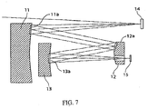
- FIG. 7 depicts an exemplary reducing projection-optical system for an X-ray projection-microlithography system.
- the depicted projection-optical system comprises aspherical X-ray reflective mirrors 11, 12, 13.
- Each mirror 11, 12, 13 has a respective effective region 11a, 12a, 13a from which the X-ray beam actually is reflected. Portions of the mirrors 11, 12, 13 located outside the respective effective regions 11a, 12a, 13a are useful for mounting and cooling the mirrors, as described later below.
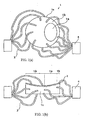
- FIGS. 1(a)-1(b) A first representative embodiment of an X-ray-reflective mirror 1 is depicted in FIGS. 1(a)-1(b).
- the subject mirror 1 comprises a mirror substrate Is defining a polished surface that has an X-ray-reflective coating 2 (e.g ., multilayer coating).
- the reflective surface includes an effective region 1a.
- the depicted region 1b is located outside the effective region 1a. Attached to various locations on the mirror 1 outside the effective region 1a are multiple thermal-transfer members 3 that serve as heat-conduction conduits for removing heat from the mirror 1.
- the mirror 1 can be mounted in a "column" (effectively a vacuum chambers) in a conventional manner (e.g ., using a plate spring or the like, not shown) in a manner such that mechanical stress from the mounting is not conveyed to the mirror.
- the depicted X-ray-reflective mirror can be used, for example, in a projection-optical system of a reducing X-ray projection-microlithography system that utilizes an EUV beam having a wavelength of 13 nm.
- the mirror substrate Is can be quartz that defines a finely polished surface.
- the X-ray-reflective coating 2 desirably is a Mo/Si multilayer coating.
- the X-ray-reflective coating 2 is not limited to a Mo/Si multilayer coating.
- the reflective coating 2 can be a multilayer coating of one or more of Si, Be, and B 4 C and one or more of Mo, Ro, and Rh, depending upon the specific wavelength employed.
- the thermal-transfer members 3 are attached individually to respective locations on the mirror 1 outside the effective region 1a, and are directed away from their respective attachment locations so as not to obstruct the effective region 1a.
- the distal ends of the thermal-transfer members 3 are attached to a cooling mechanism 4.
- the thermal-transfer members 3 and cooling mechanism 4 collectively constitute a thermal "trap" or "sink” for the mirror 1.
- Each thermal-transfer member 3 is longitudinally extended and is constructed of a material that has high thermal conductivity and that is sufficiently flexible so as not to impart, collectively or individually, any significant stress to the mirror 1.
- thermal-transfer members 3 are attached to respective locations outside the region 1b, such as on the edges and rear of the mirror substrate 1s.
- the thermal-transfer members 3 are made sufficiently flexible by reducing their individual rigidity by physical or structural means. For example, as shown, each thermal-transfer member 3 has a high ratio of length to width. By making the thermal-transfer members 3 flexible in this manner, stress imparted to the mirror 1 by thermal deformation and/or positional or postural changes of the members 3 is minimized effectively.
- the thermal-transfer members 3 desirably are made of a high-thermal-conductivity material such as copper or aluminum. Both of these materials are relatively flexible, especially when configured as structures having a high ratio of length to width. Desirably, many thermal-transfer members 3 are attached to each mirror to ensure efficient and rapid cooling of the mirror 1. From the instant disclosure, it will be understood that the number of thermal-transfer members actually employed per mirror 1 can be selected based on various factors to achieve a rate of thermal conduction sufficient to maintain mirror performance to within specification.
- a thermal-transfer member having "low rigidity” means that the rigidity of the subject thermal-transfer member effectively prevents transfer of stress to and from the mirror so as to maintain mirror performance to within specification.
- stress produced by mechanical deformation of the thermal-transfer member is not transmitted to the mirror in an amount that compromises the requisite operational precision and accuracy of the mirror.
- Exemplary materials capable of providing such low rigidity in wire or tape form, while maintaining sufficient thermal conductivity include copper and aluminum.
- the requisite low rigidity also can be achieved by configuring each thermal-transfer member with a low-rigidity structure.
- One exemplary low-rigidity structure is a wire or tape-like structure having a low transverse area relative to length.
- Another exemplary low-rigidity structure is an articulated or bellows structure.
- Attachment of the thermal-transfer members 3 to the mirror 1 desirably is performed in a manner involving direct contact of the material of each member 3 to the mirror. This is in contrast to indirect attachment, which involves use of an intermediary substance such as an adhesive. Direct attachment achieves reduced thermal resistance between the mirror and the members 3. Direct attachment can be achieved by, for example, screws or analogous fasteners, or use of a bonding agent placed over (rather than between) points of contact of the members 3 with the mirror 1.
- the cooling mechanism 4 can be, for example, a heat-exchange device through which a coolant fluid is circulated.
- Exemplary coolant fluids include liquids such as water or oil or gases such as Freon®.
- the cooling mechanism 4 can be any of various types of cooling devices.
- a single cooling mechanism 4 can be connected in this manner to the respective thermal-transfer members 3 of multiple X-ray-reflective mirrors.
- the X-ray-reflective mirror 1 is housed within a vacuum chamber or other suitable housing (not shown) providing both the requisite "column" structure and a suitable vacuum environment for the mirror.
- the cooling mechanism 4 desirably is located outside the chamber. Since, with such a configuration, the thermal-transfer members 3 extend through the wall of the vacuum chamber, an appropriate feed-through seal is required.
- FIGS. 2(a)-2(b) A second representative embodiment of an X-ray-reflective mirror 1 is depicted in FIGS. 2(a)-2(b), in which components that are similar to corresponding components of the first representative embodiment have the same respective reference numerals.
- the second representative embodiment differs from the first representative embodiment in the following aspects: (1) thermal transfer from the mirror 1 to the cooling mechanism 4 is via first thermal-transfer members 3a connected to the mirror and second thermal-transfer members 5 connecting the first thermal-transfer members 3a to the cooling mechanism 4; and (2) use of anodic welding to attach ends of the first thermal-transfer members 3a to the mirror 1.
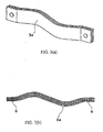
- Each first thermal-transfer member 3a comprises multiple parallel, flexible, tape-like portions, as discussed below. One end of each first thermal-transfer member 3a is attached to a respective location on the mirror 1, and the other end is attached to the second thermal-transfer member 5. Each first thermal-transfer member 3a has a length sufficient to provide compliance between the mirror 1 and the second thermal-transfer member 5 in the event of changes in the gap between the mirror 1 and the second thermal-transfer member 5. Thus, in the event of a change in said gap, stress is not imparted to the mirror 1.
- the second thermal-transfer member 5 has relatively high rigidity compared to the first thermal-transfer members 3a, stress (e.g ., from the cooling mechanism 4) is not imparted to the mirror 1 while still allowing effective conduction of heat away from the mirror 1 via the thermal-transfer members 3a, 5.
- the second thermal-transfer member 5 desirably is made of a material having high thermal conductivity. To further improve its thermal conduction, the second thermal-transfer member 5 may be hollow so as to allow cooling fluid from the cooling mechanism 4 to flow through the second thermal-transfer member 5.
- the distal ends of the first thermal-transfer members 3a can be attached to the second thermal-transfer member 5 by anodic welding or by use of mechanical fasteners such as screws or rivets made of, e.g ., copper or aluminum.
- each tape-like portion of a first thermal-transfer member 3a is made of copper with a thickness of 0.05 mm and a width of 10 mm, and with 40 tape-like portions used in each first thermal-transfer member 3a.
- An exemplary thermal conductivity is 400 W/mK at 20 °C.
- each first thermal-transfer member 3a desirably has a length of 300 mm.
- each first thermal-transfer member 3a desirably is relatively small so as to provide the lowest practical rigidity of the member (see FIG. 3(a)) without substantially compromising its thermal conductivity.
- each first thermal-transfer member 3a desirably is attached only at its respective ends 6 to the mirror 1 and second thermal-transfer member 5.
- the transverse area of each member 3a low relative to length, the collective high thermal-transfer efficacy of the members 3a can be retained by providing many members 3a between the mirror 1 and the second thermal-transfer member 5.
- adequate performance is obtained using twenty first thermal-transfer members 3a connected between the mirror 1 and the second thermal-transfer member 5.
- the first thermal-transfer members 3a need not be dimensioned identically. In any particular configuration, optimal performance of the first thermal-transfer members 3a can be obtained as appropriate by combining first thermal-transfer members 3a having transverse sections of different widths and thicknesses.
- the first thermal-transfer members 3a are attached (at their respective ends 6) to the mirror 1 desirably by anodic welding.
- the mirror 1 can be made from a glass mirror substrate, and the first thermal-transfer members 3a can be made of aluminum.
- the end 6 of a first thermal-transfer member 3a is welded anodically to the mirror 1 by applying local heat and voltage, as well as a crimping pressure, to the point of contact of the end 6 with the mirror 1.
- An anodic weld exhibits minimal thermal resistance because it lacks an interposed medium (e.g ., bonding agent or adhesive) between the end 6 and the mirror 1.
- an anodic weld is tenacious and produces substantially no outgassing, which is highly advantageous in a vacuum environment such as used in an X-ray projection-optical system.
- an anodic weld must be made to a location on a multilayer coating, either the multilayer coating at the location desirably is removed before making the weld or a material capable of being anodically welded is formed locally on the multilayer coating at the site of the weld.
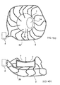
- FIGS. 4(a)-4(b) A third representative embodiment of an X-ray-reflective mirror 1 is depicted in FIGS. 4(a)-4(b), in which components that are similar to corresponding components of the first and second representative embodiments have the same respective reference numerals.
- the third representative embodiment differs from the second representative embodiment in the following aspects: (1) thermal transfer from the mirror 1 is achieved using longitudinally extended first thermal-transfer members 3b; (2) for attachment of the first thermal-transfer members 3b to the mirror 1, a metal layer 7 is formed on the surface of the mirror in the region 1b (which is outside the effective region 1a of the mirror 1); and (3) respective ends of the first thermal-transfer members 3b are weld-bonded to respective locations on the metal layer 7.
- the mirror substrate is a glassy material.
- Each of the first thermal-transfer members 3b is a respective copper wire
- the metal layer 7 is a layer of copper that is vapor-deposited on the surface of the mirror outside the effective region 1a. Weld-bonding of the ends of the first thermal-transfer members 3b to the metal layer 7 can be by spot-soldering using a solder having a low electrical resistance, such as used in connecting pin wires to respective pads on semiconductor integrated-circuit chips. Copper wire is advantageous for use in making the first thermal-transfer members 3b because such wire can have high flexibility without compromising thermal conductivity. Thus, the wires provide effective thermal-conduction paths from the mirror 1 without excessive stress being applied to the mirror.
- vapor deposition is an effective method for forming the metal layer 7 because vapor deposition results in formation of a uniform-thickness layer at all desired locations on the mirror, regardless of the shape of the mirror substrate 1.
- any of various X-ray optical systems can be constructed that comprises one or more X-ray-reflective mirrors according to one or more of the representative embodiments described above.
- such an X-ray optical system can be incorporated readily into an X-ray microlithography system (see FIG. 7).
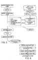
- FIG. 5 is a flowchart of an exemplary microelectronic-device-fabrication method to which apparatus and methods as described herein can be applied.
- the fabrication method generally comprises the main steps of wafer production (wafer preparation) that results in preparation of a wafer on which the microelectronic devices are formed, reticle production (reticle preparation) that results in preparation of a pattern-defining reticle used in microlithographic exposure or other suitable method for transferring the pattern from the reticle to the wafer, wafer processing that results in fabrication of the microelectronic devices on the wafer, device assembly that results in production of one or more individual functional device "chips" cut from the wafer, and inspection of completed chips.
- wafer production wafer preparation
- reticle production reticle preparation
- wafer processing that results in fabrication of the microelectronic devices on the wafer
- device assembly that results in production of one or more individual functional device "chips" cut from the wafer, and inspection of completed chips.
- Each of these steps usually comprises
- wafer processing is key to achieving the smallest feature sizes (critical dimensions) and best inter-layer registration.
- wafer-processing step multiple circuit patterns are layered successively atop one another on the wafer, wherein the formation of each layer typically involves multiple sub-steps.
- multiple operative microelectronic devices are produced on each wafer.
- Typical wafer-processing steps include: (1) thin-film formation involving formation (e.g ., by CVD or sputtering) of a dielectric layer for insulation or a metal layer for forming electrodes or for connecting wires, (2) an oxidation step that oxidizes the thin-film layer or the wafer substrate; (3) microlithography, using a reticle, that forms a resist pattern for selective processing of the thin film or the substrate itself, (4) etching or analogous step (e.g ., dry-etching) to etch the thin film or substrate according to the resist pattern, (5) doping as required to implant and diffuse ions or impurities into the thin film or substrate according to the resist pattern, (6) resist-stripping to remove the resist from the wafer, and (7) wafer inspection to assess the results of steps (1)-(6). Wafer processing is repeated as required (typically many times to form the many layers normally required) to fabricate the desired microelectronic devices on the wafer.
- FIG. 6 provides a flowchart of typical steps performed in microlithography, which is a principal step in wafer processing.
- the microlithography step typically includes: (1) resist-coating step, in which a suitable resist is coated on the wafer substrate (which can include circuit elements formed in a previous wafer-processing step), (2) exposure step, to expose the resist with the desired pattern, (3) development step, to develop the exposed resist and obtain the desired pattern in the resist, and (4) optional annealing step, to stabilize and/or enhance the durability of the resist pattern as formed in the resist.
- the exposure step involves microlithography performed using a microlithography system that includes an X-ray optical system comprising one or more X-ray-reflective mirrors as described above. Since the constituent X-ray-reflective mirrors exhibit reduced stress-related deformation (including thermal stress), enhanced microlithographic accuracy and precision is obtained using the system.
Landscapes
- Physics & Mathematics (AREA)
- Spectroscopy & Molecular Physics (AREA)
- Engineering & Computer Science (AREA)
- General Engineering & Computer Science (AREA)
- High Energy & Nuclear Physics (AREA)
- Exposure And Positioning Against Photoresist Photosensitive Materials (AREA)
- Exposure Of Semiconductors, Excluding Electron Or Ion Beam Exposure (AREA)
- Optical Elements Other Than Lenses (AREA)
- Mounting And Adjusting Of Optical Elements (AREA)
Applications Claiming Priority (2)
| Application Number | Priority Date | Filing Date | Title |
|---|---|---|---|
| JP2002018205 | 2002-01-28 | ||
| JP2002018205A JP2003218023A (ja) | 2002-01-28 | 2002-01-28 | X線反射鏡、x線露光転写装置及び半導体デバイスの製造方法 |
Publications (1)
| Publication Number | Publication Date |
|---|---|
| EP1331646A2 true EP1331646A2 (de) | 2003-07-30 |
Family
ID=19192081
Family Applications (1)
| Application Number | Title | Priority Date | Filing Date |
|---|---|---|---|
| EP03001788A Withdrawn EP1331646A2 (de) | 2002-01-28 | 2003-01-28 | Röntgenstrahlen reflektierende Spiegel mit verminderten thermischen Spannungen und Röntgenstrahloptische Systeme mit diesen Spiegeln |
Country Status (3)
| Country | Link |
|---|---|
| US (1) | US20030142785A1 (de) |
| EP (1) | EP1331646A2 (de) |
| JP (1) | JP2003218023A (de) |
Families Citing this family (9)
| Publication number | Priority date | Publication date | Assignee | Title |
|---|---|---|---|---|
| US7274430B2 (en) * | 1998-02-20 | 2007-09-25 | Carl Zeiss Smt Ag | Optical arrangement and projection exposure system for microlithography with passive thermal compensation |
| JP4590205B2 (ja) * | 2003-05-14 | 2010-12-01 | キヤノン株式会社 | ミラー保持方法、光学装置、露光装置、およびデバイス製造方法 |
| JP2005083862A (ja) * | 2003-09-08 | 2005-03-31 | Canon Inc | 光学薄膜およびこれを用いたミラー |
| JP2005175187A (ja) * | 2003-12-11 | 2005-06-30 | Canon Inc | 光学部材、冷却方法、冷却装置、露光装置、デバイス製造方法、及びデバイス |
| US7235801B2 (en) * | 2004-06-04 | 2007-06-26 | Asml Netherlands B.V. | Grazing incidence mirror, lithographic apparatus including a grazing incidence mirror, method for providing a grazing incidence mirror, method for enhancing EUV reflection of a grazing incidence mirror, device manufacturing method and device manufactured thereby |
| DE102008049556B4 (de) * | 2008-09-30 | 2011-07-07 | Carl Zeiss SMT GmbH, 73447 | Mikrolithographische Projektionsbelichtungsanlage |
| JP5756982B2 (ja) * | 2009-12-28 | 2015-07-29 | 株式会社ジェイテック | X線集光方法、反射面形状制御ミラー装置及び反射面形状制御ミラーの製造方法 |
| US8643823B2 (en) * | 2010-02-23 | 2014-02-04 | Media Lario S.R.L. | Stress-decoupling devices and methods for cooled mirror systems |
| CN113936840B (zh) * | 2021-10-22 | 2023-08-25 | 中国科学院上海高等研究院 | 一种温控x射线变形镜 |
Family Cites Families (7)
| Publication number | Priority date | Publication date | Assignee | Title |
|---|---|---|---|---|
| JPH08222497A (ja) * | 1995-02-09 | 1996-08-30 | Nikon Corp | 反射型マスク |
| JPH11243052A (ja) * | 1997-11-14 | 1999-09-07 | Nikon Corp | 露光装置 |
| DE19807094A1 (de) * | 1998-02-20 | 1999-08-26 | Zeiss Carl Fa | Optische Anordnung und Projektionsbelichtungsanlage der Mikrolithographie mit passiver thermischer Kompensation |
| US6377655B1 (en) * | 1998-05-08 | 2002-04-23 | Nikon Corporation | Reflective mirror for soft x-ray exposure apparatus |
| JPH11345760A (ja) * | 1998-05-29 | 1999-12-14 | Nikon Corp | 露光装置 |
| JP2000349009A (ja) * | 1999-06-04 | 2000-12-15 | Nikon Corp | 露光方法及び装置 |
| JP2001242364A (ja) * | 2000-03-01 | 2001-09-07 | Canon Inc | 光学素子の保持機構、および該保持機構によって構成された投影光学系を備える露光装置 |
-
2002
- 2002-01-28 JP JP2002018205A patent/JP2003218023A/ja active Pending
-
2003
- 2003-01-28 US US10/353,467 patent/US20030142785A1/en not_active Abandoned
- 2003-01-28 EP EP03001788A patent/EP1331646A2/de not_active Withdrawn
Also Published As
| Publication number | Publication date |
|---|---|
| JP2003218023A (ja) | 2003-07-31 |
| US20030142785A1 (en) | 2003-07-31 |
Similar Documents
| Publication | Publication Date | Title |
|---|---|---|
| US6048652A (en) | Backside polish EUV mask and method of manufacture | |
| JP2023052147A (ja) | 合金吸収体を有する極紫外線マスクブランク、及びその製造方法 | |
| TWI434132B (zh) | 具有高熱傳導性之極紫外線主光罩基板 | |
| US6833223B2 (en) | Multilayer-film reflective mirrors and optical systems comprising same | |
| US6803994B2 (en) | Wavefront aberration correction system | |
| US8425060B2 (en) | Self-correcting optical elements for high-thermal-load optical systems | |
| US20090122428A1 (en) | Reflective optical elements exhibiting multimetallic-like self-correction of distortions caused by heating | |
| EP0279670A2 (de) | Reflexionsmaske | |
| US20090147386A1 (en) | Temperature-regulating devices for reflective optical elements | |
| EP0955565A2 (de) | Spiegel für einen Belichtungsapparat unter Verwendung weicher Röntgenstrahlen | |
| US20070248127A1 (en) | Optical-element-cooling devices and exposure apparatus comprising optical elements including same | |
| TW201736941A (zh) | 用於極紫外線微影之薄膜 | |
| WO1999045581A1 (en) | Method and apparatus for exposure, method of manufacture of exposure tool, device, and method of manufacture of device | |
| US20040089818A1 (en) | Multi-foil optic | |
| US20030142785A1 (en) | X-ray-reflective mirrors exhibiting reduced thermal stress, and X-ray optical systems comprising same | |
| US20050128448A1 (en) | Lithographic apparatus and device manufacturing method | |
| JP2007142190A (ja) | 露光装置及びデバイス製造方法 | |
| US7470916B2 (en) | Lithographic apparatus, device manufacturing method and radiation collector | |
| TW200527499A (en) | Lithographic apparatus and device manufacturing method | |
| JP4567659B2 (ja) | リソグフィ装置およびデバイス製造方法 | |
| EP1995767A1 (de) | Optisches projektionssystem, ausrichtvorrichtung und verfahren zum herstellen von halbleiterbauelementen | |
| JP4599334B2 (ja) | 物品支持部材を製造する方法 | |
| JP4305003B2 (ja) | Euv光学系及びeuv露光装置 | |
| JPH11345760A (ja) | 露光装置 | |
| JP2004134743A (ja) | リソグラフ装置およびデバイス製造方法 |
Legal Events
| Date | Code | Title | Description |
|---|---|---|---|
| PUAI | Public reference made under article 153(3) epc to a published international application that has entered the european phase |
Free format text: ORIGINAL CODE: 0009012 |
|
| AK | Designated contracting states |
Designated state(s): AT BE BG CH CY CZ DE DK EE ES FI FR GB GR HU IE IT LI LU MC NL PT SE SI SK TR |
|
| AX | Request for extension of the european patent |
Extension state: AL LT LV MK RO |
|
| RIN1 | Information on inventor provided before grant (corrected) |
Inventor name: KAGEYAMA, MOTOFUSAC/O NIKON CORPORATION |
|
| STAA | Information on the status of an ep patent application or granted ep patent |
Free format text: STATUS: THE APPLICATION HAS BEEN WITHDRAWN |
|
| 18W | Application withdrawn |
Effective date: 20080311 |