EP1329936A1 - Phasenkontrast-Elektronenmikroskop mit ringförmiger Beleuchtungsapertur - Google Patents
Phasenkontrast-Elektronenmikroskop mit ringförmiger Beleuchtungsapertur Download PDFInfo
- Publication number
- EP1329936A1 EP1329936A1 EP02023322A EP02023322A EP1329936A1 EP 1329936 A1 EP1329936 A1 EP 1329936A1 EP 02023322 A EP02023322 A EP 02023322A EP 02023322 A EP02023322 A EP 02023322A EP 1329936 A1 EP1329936 A1 EP 1329936A1
- Authority
- EP
- European Patent Office
- Prior art keywords
- phase
- electron microscope
- shifting element
- microscope according
- transmission electron
- Prior art date
- Legal status (The legal status is an assumption and is not a legal conclusion. Google has not performed a legal analysis and makes no representation as to the accuracy of the status listed.)
- Granted
Links
Images


Classifications
-
- H—ELECTRICITY
- H01—ELECTRIC ELEMENTS
- H01J—ELECTRIC DISCHARGE TUBES OR DISCHARGE LAMPS
- H01J37/00—Discharge tubes with provision for introducing objects or material to be exposed to the discharge, e.g. for the purpose of examination or processing thereof
- H01J37/26—Electron or ion microscopes; Electron or ion diffraction tubes
- H01J37/261—Details
- H01J37/265—Controlling the tube; circuit arrangements adapted to a particular application not otherwise provided, e.g. bright-field-dark-field illumination
-
- H—ELECTRICITY
- H01—ELECTRIC ELEMENTS
- H01J—ELECTRIC DISCHARGE TUBES OR DISCHARGE LAMPS
- H01J37/00—Discharge tubes with provision for introducing objects or material to be exposed to the discharge, e.g. for the purpose of examination or processing thereof
- H01J37/26—Electron or ion microscopes; Electron or ion diffraction tubes
-
- H—ELECTRICITY
- H01—ELECTRIC ELEMENTS
- H01J—ELECTRIC DISCHARGE TUBES OR DISCHARGE LAMPS
- H01J2237/00—Discharge tubes exposing object to beam, e.g. for analysis treatment, etching, imaging
- H01J2237/26—Electron or ion microscopes
- H01J2237/2614—Holography or phase contrast, phase related imaging in general, e.g. phase plates
Definitions
- phase contrast microscopy is of great importance for the Visualization of biological structures that have little or no Generate amplitude contrast.
- the phase contrast is generated by that by a phase plate different diffraction orders of the diffracted on the object Radiation, which due to the diffraction effect already has a phase difference of ⁇ / 2 have an additional, different for the different diffraction orders Phase shift of ⁇ / 2 is also impressed.
- the undeflected light on the object is impressed by a phase shift which differs by ⁇ / 2 from that of the higher diffraction orders impressed phase shift differs.
- This method is based on electron optics not easily transferable, because on the one hand due to the small lighting aperture submicroscopic ring diaphragm would be required in the lighting system and on the other hand no suitable carrier material that is completely transparent to electrons is available.
- phase contrast transfer function phase contrast transfer function
- phase contrast in electron microscopy is in an essay by Boersch in Zeitschrift für Naturwissenschaften 2a, 1947, page 615 ff. described. Then the phase shift of the electron beam by external electrical and / or magnetic potentials or by utilizing the inner potential exploited when passing through a thin film.
- the latter principle exists Phase plate made of a thin carbon film with a thickness of 20nm with a central one Hole through which the zero beam can pass unaffected. The deflected rays step through the film and experience a phase shift of ⁇ / 2.
- this principle has major disadvantages.
- the manufacture and Centering such small holes relative to the electron beam is very problematic.
- the thickness of the film can change significantly due to contamination and the central one Hole for the zero beam can quickly become overgrown due to contamination.
- the inevitable electrical charging of the film causes an additional anisotropic phase shift which makes the overall phase shift relatively uncontrollable.
- the higher orders of diffraction of the radiation diffracted at the object, that of its Intensity are already weaker than the zero beam, because of the foil weakened in their intensity by elastic and inelastic scattering, so that the generated Contrast is correspondingly weak.
- the aim of the present invention is therefore to provide an electron microscope with which the generation of easily interpretable phase contrast images is possible and none with regard to the production and permanent maintenance of critical components having.
- no self-supporting structures i.e. Structures over thin Retaining bars are held across the area for the creation of the figure bridge required beam cross-section, may be required.
- the phase contrast is very similar to Generation of the phase contrast generated in light microscopy.
- the lighting system of the electron microscope is generated in an object plane to be imaged Fourier-transformed plane an annular lighting aperture. Like in the Phase contrast light microscopy is therefore used to illuminate the image to be imaged Object with a hollow cone-shaped beam.
- a phase-shifting element is arranged on the plane or on a conjugate plane of the object in undiffracted radiation, i.e. the zero beam, compared to that on the object in higher diffraction orders diffracted radiation a phase shift.
- the phase-shifting element leaves the phase of the object higher Diffraction orders diffracted radiation that is closer to the optical in the radial direction Axis run as the zero beam, unaffected or influences it only slightly.
- phase-shifting element In the transmission electron microscope according to the invention, as in the case of Phase contrast in light microscopy of the phase-shifting element on the object undiffracted radiation compared to the radiation diffracted at the object Phase shift granted.
- the optical axis runs as the radiation that is not diffracted at the object, but is phase-shifting element is not affected.
- a corresponding phase-shifting element can therefore be annular with a central opening. Such an annular one phase-shifting element can therefore be taken on its outer circumference, so that no self-supporting or almost self-supporting structures are required.
- phase-shifting element or one Holding structure of the phase-shifting element in relation to the zero beam in a radial Direction of higher diffraction orders further from the optical axis fades. Because this is the negative influence of extra-axial aberrations of the Lens reduced.
- the phase-shifting element preferably not only influences the phase of the Zero beam but at the same time weakens the intensity via a corresponding absorption of the zero beam. Because of the intensity adjustment that can be achieved between the zero beam and the higher diffraction orders achieve an overall contrast improvement.
- a combination of the phase-shifting element with an aperture diaphragm can be used Realize very stable construction of the phase-shifting element.
- the one to the optical axis Deflected radiation of higher order can pass through the central opening of the pass through the phase-shifting element, while that of the optical axis in Radiation diffracted radiation is hidden. Goes through this blanking however, no information is lost since the 180 ° with respect to the optical axis twisted illuminating beam the complementary information to the hidden Contains diffraction orders.
- a corresponding phase-shifting element is technologically simple to implement. Through its unimpeded passage through the phase-shifting element, the Diffracted radiation of higher order carrying information neither by the structure of the phase-shifting element has a negative influence due to its mounting, like a weakening or additional phase shift. In addition, none in certain spatial directions, diffracted radiation completely through holding structures hidden.
- the corresponding phase-shifting element can rather be formed rotationally symmetrical to the optical axis.
- phase-shifting element There are also small holes in the phase-shifting element through which the primary beam must pass through; avoided. Negative influences from otherwise with small holes Contamination effects are largely excluded. And there only the zero-order diffraction order carrying no information about the object If the phase-shifting element passes through, variations of Phase shift due to local fluctuations in the thickness of the phase-shifting element statistically.
- the phase-shifting element is as Ring electrode formed, the electrostatic potential is variable.
- the phase-shifting element is as annular film is formed, which is received on a solid support. Both the annular film and the solid support each have a perpendicular to the optical Axis aligned opening, the opening diameter of the annular film is smaller than the opening diameter of the solid support.
- the massive carrier can then at the same time as an aperture diaphragm to mask out those that are bent away from the optical axis serve higher diffraction orders.
- annular illumination aperture is preferably in a Object level conjugate level provided a deflection system.
- the annular illumination aperture is sequentially timed by varying the Deflection angle generated.
- An alternative generation of the ring-shaped illumination aperture is also through a corresponding aperture with central shading in the light beam path possible. Furthermore, it is particularly useful in thermal emitters as an electron source possible, the underheated cathode image (hollow jet), which is already an annular Has emission distribution with a weak central maximum, in the front To map the focal plane of the condenser lens single-field lens and the central one Hide emission spot to create the circular illumination aperture.
- the underheated cathode image which is already an annular Has emission distribution with a weak central maximum
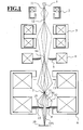
- the transmission electron microscope shown in FIG. 1 has a beam generator (1) and a total of three-stage condenser (2, 3, 6).
- the jet generator (1) is preferably a field emission source or a Schottky emitter.
- the first condenser lens (2) generates a real image (12) of the crossover (11) of the beam generator (1).
- This real Crossover image (12) is real from the following second condenser lens (3) source focal plane (13) of the third condenser lens (6) is shown.
- the third Condenser lens (6) is a so-called condenser lens single field lens, the apron as Condenser lens and its rear field serves as an objective lens and in which the object plane (7) is in the middle of the pole shoe gap of the condenser-objective single-field lens (6).
- the object plane (7) Through the Image of the crossover (11) of the particle generator (1) in the source-side focal plane (13) the condenser-objective single-field lens (6), the object plane (7) through a parallel Illuminated particle beam aligned to the optical axis.
- the corresponding one Illumination beam path is shown in dashed lines in FIG. 1.
- the particle beam is conjugated to each object point Point (14) in the plane of the field diaphragm (5) tilted by the same angle.
- this Deflection or tilting of the particle beam is a corresponding tilting of the Particle beam generated in the object plane (7).
- a rotating beam results in the object plane (7) or one in time corresponds to sequential hollow-cone-shaped illumination aperture.
- the amplitude of the deflection generated by the deflection system (4) is the inside diameter the ring-shaped lighting aperture is determined and adjustable.
- the ring diameter of the ring-shaped illumination aperture is determined by the imaging scale with that of the crossover (11) of the particle beam generator (1) into the source-side focal plane (13) the condenser-objective single-field lens (6) is shown.
- the rear field or imaging field of the condenser-objective single-field lens (6) Beam cone with temporally sequential hollow cone-shaped illumination aperture in the Intermediate image plane (10) focused so that in the intermediate image plane (10) a real image of the Object level (7) is created.
- the annular phase-shifting element (9) is added in the rear focal plane (15) on the intermediate image side Condenser-objective single field lens in the area of the central opening of an aperture diaphragm (8) the annular phase-shifting element (9) is added.
- This ring-shaped phase-shifting element has a large central opening (19) - with a diameter of a few 10 ⁇ m, preferably at least 30 ⁇ m -, by which the compared to the undeflected radiation (zero beam) (50) in the direction of the optical axis (OA) Higher order radiation (51) can pass through unhindered.
- phase-shifting element (9) of the undeflected radiation on the object that is, the zero beam (50)
- a phase shift of preferably ⁇ / 2 In the intermediate image plane (10) takes place a superposition of the phase-shifted zero beam (50) with that in the direction of the optical axis diffracted radiation (51) instead.
- Those higher on the object Diffraction orders (52) opposite in the plane of the phase-shifting element (9) of the undeflected radiation are further away from the optical axis however, absorbed by the aperture diaphragm (8).
- FIG. 2 With regard to the positions of the different diffraction orders relative to phase-shifting element (9) and the resulting functioning of the The arrangement according to the invention is referred to FIG. 2.
- the arrangement according to the invention is referred to FIG. 2.
- Both the plus first as well the minus first diffraction order (51) in the plane of the phase-shifting element run closer to the optical axis than the zero beam, pass through the central one unaffected Opening (10) in the phase-shifting element (9).
- the undiffracted on the specimen Radiation experiences the ring-shaped phase-shifting element (9) desired phase shift and the desired attenuation, while the two higher diffraction orders (52) further from the axis completely from the diaphragm (8) be eliminated.
- each point in the Object plane (7) illuminated with an electron beam which is a hollow cone Has lighting aperture.
- the tip of the illuminating beam cone lies in the Object level (7).
- the bundle of rays emanating from the object level divergent, hollow-cone-shaped illumination aperture is created by the rear field of the condenser-objective single-field lens (6) in the intermediate image plane (10).
- FIG. 3a A first exemplary embodiment of a phase-shifting element is shown in FIG. 3a shown. It has an annular support structure (8) made of an electrically conductive material on.
- the support structure (8) has a central opening (19). In the area of the central opening (19) a thin annular membrane (9) is received on the support structure (8) protrudes slightly into the central opening (19) of the support structure (8).
- the support structure (8) also serves as an aperture diaphragm to hide those away from the optical axis diffracted higher order radiation. Due to the low protrusion of the film and the Radial connection of the film membrane (9) over the full diameter to the support structure (8) there is a mechanically and electrically very stable structure. Any charges the film are avoided in that the charges flow over the support structure (8) can.
- the embodiment in Figure 3b differs from the embodiment in Figure 3a only in that the phase-shifting element (9) formed as a thin membrane two thin holding webs (17, 18) (a third holding web is in the in Figure 3b cut away area and is therefore not visible) on the support structure (16) is included.
- This embodiment in Figure 3b compared to Embodiment in Figure 3a the advantage that also away from the optical axis diffracted higher diffraction orders can contribute to image formation, however Cost of less stability and more technical effort.
- the membrane (9) can be electrical isolated on the respective support structure (8, 16) so that the membrane an electrical potential can be applied to the supporting structure. This allows the phase-shifting effect to be varied.
- FIG. 4 shows a relatively simple exemplary embodiment for an electrostatic one phase-shifting element shown.
- This phase-shifting element contains three coaxial to each other, arranged one behind the other in the direction of the optical axis Ring electrodes (20, 21, 23) with a circular central opening (24).
- the insulator (22) is the central electrode (23) with respect to the two outer ring electrodes (20, 21) isolated.
- the two outer ring electrodes (20, 21) are at the same potential, the potential of the electron-optical tube in the area of the phase-shifting Elementes, and the center electrode (23) via a voltage supply (25) on a different potential can be applied to the outer electrodes (20, 21).
- the Zero beam through the potential difference between the center electrode (23) and the two outer electrodes (20, 21) a phase shift, while towards the optical axis (center of the central opening 24) diffracted higher order radiation none or only experiences a slight constant phase shift.
- the electrode geometry is used for Suppression of higher diffraction orders from the object away from the optical axis have been bowed.
- This simple embodiment for an electrostatic phase-shifting element delivers satisfactory results, particularly in systems where the jet generator only produces a small lighting aperture, in particular in systems with Field emission source or Schottky emitter.
- the reason for this is that the phase shift as Function of the distance from the center of the central opening (24) square to this Center distance runs. The result of this is that rays far from the center are clearly visible experience greater phase shift than near-center rays. Within everyone Diffraction order, however, the phase shift is therefore not constant but special increases from the inside out, which is particularly the case with large lighting apertures Drawbacks.
- the central opening (24) of the three electrodes arranged coaxially to one another (20, 21, 23) has an inner diameter of approx. 50 ⁇ m and is therefore technologically simple manageable dimensions.
- FIG. 5 Another embodiment shown in Figure 5 for an electrostatic phase-shifting element has a somewhat difference compared to the embodiment in FIG more complex structure.
- the center electrode (39) is insulated from the other electrodes via an insulator (32).
- the outside diameter of this ring-shaped Shield electrode is smaller than the inner diameter of the central opening in the two outer electrodes (30, 31) so that between the shielding electrode (33) and the outer Electrodes (30, 31) an annular gap (35) is provided.
- This annular gap (35) serves for the passage of the zero beam.
- the shielding electrode (33) has a radial Direction of a recess (36) in which another via an insulator (37) Ring electrode (38) is added.
- the in the recess of the shielding electrode (33) arranged further ring electrode (38) is the middle electrode (39) of the three outer Ring electrodes (30, 31, 39) opposite.
- the two outer electrodes (30, 31) and Shielding electrode (33) at the same potential, while the two inner ones Ring electrodes (38, 39) by means of a voltage supply (40) with one of them deviating potential can be applied.
- This potential difference between the two inner electrodes (38, 39) and the outer electrodes (30, 31, 33) is again so set that the zero beam passing through the annular opening (35) desired phase shift of ⁇ / 2 experiences.
- Through the shielding electrode (33) ensures that the inside of the circular opening of the shielding electrode (33) Potential is constant and consequently the higher diffraction orders on the object diffracted radiation experience no phase shift.
- the embodiment in FIG. 5 is more complex to manufacture than the embodiment in Figure 4, but at the same time it is achieved that the Phase shift that the zero beam experiences, is constant over the aperture and also that higher diffraction orders experience no phase shift at all.
- phase-shifting elements designed as a membrane
- they deliver as Ring electrode or ring electrodes formed phase-shifting elements accordingly the embodiments in Figures 4 and 5 the advantage that the phase shift without Passing through a disruptive material and that occurs by varying the potential between the inner ring electrode / inner ring electrodes and the outer electrodes can set a variable phase shift.
Landscapes
- Chemical & Material Sciences (AREA)
- Analytical Chemistry (AREA)
- Analysing Materials By The Use Of Radiation (AREA)
- Electron Sources, Ion Sources (AREA)
Abstract
Description
- Fig. 1
- eine Prinziskizze eines erfindungsgemäßen Transmissions-Elektronenmikroskopes im Schnitt;
- Fig. 2
- einen Ausschnitt aus der Prinzipskizze in Figur 1;
- Fig. 3a und 3b
- zwei Ausführungsbeispiele für phasenschiebende Elemente in Form einer Folie in einer geschnittenen perspektivischen Ansicht;
- Fig. 4 und 5
- zwei Ausführungsbeispiele für phasenschiebende Elemente als Ringelektrode ausgebildet in einer geschnittenen perspektivischen Ansicht.
Claims (11)
- Transmissions-Elektronenmikroskop mit einer optischen Achse (OA), einem Beleuchtungssystem (1, 2, 3, 4) zur Ausleuchtung eines in einer Objektebene (7) zu positionierenden Objektes mit einem Elektronenstrahl und einem Objektiv (6) zur Abbildung des ausgeleuchteten Objektes, wobei der Elektronenstrahl am Objekt in einen Nullstrahl und höhere Beugungsordnungen aufgespalten wird, wobei das Beleuchtungssystem in einer zur Objektebene (7) fouriertransformierten Ebene eine ringförmige Beleuchtungsapertur erzeugt und wobei in einer von der Objektebene (7) abgewandten Brennebene (15) des Objektivs (6) oder einer dazu konjugierten Ebene ein phasenschiebendes Element (9) angeordnet ist, das dem Nullstrahl (50) gegenüber der am Objekt in höheren Beugungsordnungen (51) gebeugten Strahlung eine Phasenverschiebung erteilt und wobei das phasenschiebende Element (9) die Phase der am Objekt in höheren Beugungsordnungen (51) gebeugten Strahlung, die in radialer Richtung näher an der optischen Achse als der Nullstrahl (50) verläuft, nicht oder nur geringfügig beeinflußt.
- Transmissions-Elektronenmikroskop nach Anspruch 1, wobei das phasenschiebende Element (9) oder eine Haltestruktur (8) der selben die gegenüber dem Nullstrahl (50) in radialer Richtung weiter von der optischen Achse (OA) entfernt liegenden höheren Beugungsordnungen ausblendet.
- Transmissions-Elektronenmikroskop nach Anspruch 1 oder 2, wobei das phasenschiebende Element (9) ringförmig mit einer zentralen Öffnung (19) ausgebildet ist.
- Transmissions-Elektronenmikroskop nach einem der Ansprüche 1 - 3, wobei das phasenschiebende Element (9) den Nullstrahl (50) in der Intensität abschwächt.
- Transmissions-Elektronenmikroskop nach einem der Ansprüche 1 - 4, wobei als Elektronenquelle eine Feldemissionsquelle (1) oder ein Schottky Emitter vorgesehen ist.
- Transmissions-Elektronenmikroskop nach einem der Ansprüche 1 - 5, wobei das phasenschiebende Element eine Ringelektrode (23, 38, 39) aufweist.
- Transmissions-Elektronenmikroskop nach Anspruch 6, wobei das Potential der Ringelektrode (23, 38, 39) gegenüber dem Umgebungspotential variierbar ist.
- Transmissions-Elektronenmikroskop nach einem der Ansprüche 1 - 5, wobei das phasenschiebende Element (9) als ringförmige Folie an einem massiven Träger (8, 16) ausgebildet ist, wobei die ringförmige Elektrode (9) und der massive Träger (8, 16) jeweils eine senkrecht zur optischen Achse (OA) ausgerichtete Öffnung aufweisen und wobei der Öffnungsdurchmesser der Folie (9) kleiner als der Öffnungsdurchmesser des Trägers (8, 16) ist.
- Transmissions-Elektronenmikroskop nach Anspruch 8, wobei die ringförmige Folie (9) gegenüber dem Träger (8, 16) elektrisch isoliert ist.
- Transmissios-Elektronenmikroskop nach einem der Ansprüche 1 - 9, wobei in einer zur Objektebene (7) quellenseitigen, konjugierten Ebene ein Ablenksystem (4) für eine zeitlich sequentielle Erzeugung der ringförmigen Beleuchtungsapertur angeordnet ist.
- Transmissions-Elektronenmikroskop nach Anspruch 10, wobei das Ablenksystem (4) eine Ablenkung des Elektronenstrahls in zwei zueinander senkrechten Richtungen erzeugt, und wobei die Ablenkung in einer Richtung sinusförmig und in der dazu senkrechten Richtung cosinusförmig als Funktion der Zeit erfolgt, und wobei die Amplitude der sinus- bzw. cosinusförmigen Ablenkung identisch und zeitlich konstant ist.
Applications Claiming Priority (2)
| Application Number | Priority Date | Filing Date | Title |
|---|---|---|---|
| DE10200645A DE10200645A1 (de) | 2002-01-10 | 2002-01-10 | Elektronenmikroskop mit ringförmiger Beleuchtungsapertur |
| DE10200645 | 2002-01-10 |
Publications (2)
| Publication Number | Publication Date |
|---|---|
| EP1329936A1 true EP1329936A1 (de) | 2003-07-23 |
| EP1329936B1 EP1329936B1 (de) | 2006-11-29 |
Family
ID=7711805
Family Applications (1)
| Application Number | Title | Priority Date | Filing Date |
|---|---|---|---|
| EP02023322A Expired - Lifetime EP1329936B1 (de) | 2002-01-10 | 2002-10-18 | Phasenkontrast-Elektronenmikroskop mit ringförmiger Beleuchtungsapertur |
Country Status (4)
| Country | Link |
|---|---|
| US (1) | US6797956B2 (de) |
| EP (1) | EP1329936B1 (de) |
| JP (1) | JP4372425B2 (de) |
| DE (2) | DE10200645A1 (de) |
Cited By (6)
| Publication number | Priority date | Publication date | Assignee | Title |
|---|---|---|---|---|
| WO2003068399A3 (de) * | 2002-02-18 | 2004-02-05 | Max Planck Gesellschaft | Phasenplatte für die elektronenmikroskopie und elektronenmikroskopische bildgebung |
| US6797956B2 (en) | 2002-01-10 | 2004-09-28 | Leo Elektronenmikroskopie Gmbh | Electron microscope with annular illuminating aperture |
| WO2007022862A3 (de) * | 2005-08-24 | 2007-05-03 | Univ Karlsruhe | Verfahren zum herstellen einer mehrschichtigen elektrostatischen linsenanordnung |
| EP1835523A3 (de) * | 2006-03-14 | 2008-03-05 | Carl Zeiss NTS GmbH | Phasenkontrast-Elektronenmikroskop |
| NL2003342C2 (nl) * | 2008-08-14 | 2011-11-01 | Zeiss Carl Nts Gmbh | Deeltjesstraaltoestel met ringvormige belichtingsapertuur. |
| EP2159818B1 (de) * | 2008-08-27 | 2015-03-18 | Max-Planck-Gesellschaft zur Förderung der Wissenschaften e.V. | Elektronenmikroskop mit einer Phasenplatte |
Families Citing this family (23)
| Publication number | Priority date | Publication date | Assignee | Title |
|---|---|---|---|---|
| JP4328044B2 (ja) * | 2001-09-25 | 2009-09-09 | 日本電子株式会社 | 差分コントラスト電子顕微鏡および電子顕微鏡像のデータ処理方法 |
| US20030085350A1 (en) * | 2001-11-02 | 2003-05-08 | Kazutoshi Kaji | Ultimate analyzer, scanning transmission electron microscope and ultimate analysis method |
| US7737412B2 (en) * | 2004-07-12 | 2010-06-15 | The Regents Of The University Of California | Electron microscope phase enhancement |
| JP2006059513A (ja) * | 2004-07-22 | 2006-03-02 | Kuresutetsuku:Kk | 電子ビーム照射装置および描画装置 |
| JP4625317B2 (ja) * | 2004-12-03 | 2011-02-02 | ナガヤマ アイピー ホールディングス リミテッド ライアビリティ カンパニー | 位相差電子顕微鏡用位相板及びその製造方法並びに位相差電子顕微鏡 |
| DE102006055510B4 (de) * | 2006-11-24 | 2009-05-07 | Ceos Corrected Electron Optical Systems Gmbh | Phasenplatte, Bilderzeugungsverfahren und Elektronenmikroskop |
| DE102007007923A1 (de) * | 2007-02-14 | 2008-08-21 | Carl Zeiss Nts Gmbh | Phasenschiebendes Element und Teilchenstrahlgerät mit phasenschiebenden Element |
| US8642959B2 (en) * | 2007-10-29 | 2014-02-04 | Micron Technology, Inc. | Method and system of performing three-dimensional imaging using an electron microscope |
| DE102009016861A1 (de) | 2009-04-08 | 2010-10-21 | Carl Zeiss Nts Gmbh | Teilchenstrahlmikroskop |
| JP5476146B2 (ja) * | 2010-02-03 | 2014-04-23 | 日本電子株式会社 | 透過電子顕微鏡の制御装置および透過電子顕微鏡の制御方法 |
| JP5319579B2 (ja) * | 2010-03-05 | 2013-10-16 | 株式会社日立製作所 | 位相差電子顕微鏡および位相板 |
| JP5564292B2 (ja) * | 2010-03-05 | 2014-07-30 | 株式会社日立製作所 | 位相板およびこれを用いた位相差電子顕微鏡 |
| WO2011163397A1 (en) * | 2010-06-22 | 2011-12-29 | The Regents Of The University Of California | Microfabricated high-bandpass foucault aperture for electron microscopy |
| USD654147S1 (en) | 2011-04-06 | 2012-02-14 | The Clorox Company | Faucet mount device with pressure fit |
| USD654146S1 (en) | 2011-04-06 | 2012-02-14 | The Clorox Company | Faucet mount device with flip configuration |
| JP5897888B2 (ja) * | 2011-12-07 | 2016-04-06 | 株式会社ニューフレアテクノロジー | 荷電粒子ビーム描画装置 |
| EP2667399A1 (de) * | 2012-05-23 | 2013-11-27 | FEI Company | Verbesserte Phasenplatte für ein TEM |
| JP6286270B2 (ja) | 2013-04-25 | 2018-02-28 | エフ イー アイ カンパニFei Company | 透過型電子顕微鏡内で位相版を用いる方法 |
| DE102013019297A1 (de) | 2013-11-19 | 2015-05-21 | Fei Company | Phasenplatte für ein Transmissionselektronenmikroskop |
| US10535497B2 (en) | 2016-08-22 | 2020-01-14 | Hitachi High-Technologies Corporation | Electron microscope and imaging method |
| JP7193694B2 (ja) | 2018-07-26 | 2022-12-21 | 国立研究開発法人理化学研究所 | 電子顕微鏡およびそれを用いた試料観察方法 |
| WO2020152795A1 (ja) * | 2019-01-23 | 2020-07-30 | 株式会社日立ハイテク | 電子ビーム観察装置、電子ビーム観察システム、電子ビーム観察装置における画像補正方法及び画像補正のための補正係数算出方法 |
| JP6995103B2 (ja) * | 2019-11-15 | 2022-01-14 | 日本電子株式会社 | 透過電子顕微鏡および透過電子顕微鏡の制御方法 |
Citations (2)
| Publication number | Priority date | Publication date | Assignee | Title |
|---|---|---|---|---|
| JPS607048A (ja) * | 1983-06-24 | 1985-01-14 | Hitachi Ltd | 位相差電子顕微鏡 |
| US5814815A (en) * | 1995-12-27 | 1998-09-29 | Hitachi, Ltd. | Phase-contrast electron microscope and phase plate therefor |
Family Cites Families (3)
| Publication number | Priority date | Publication date | Assignee | Title |
|---|---|---|---|---|
| JP2002153271A (ja) * | 2000-11-17 | 2002-05-28 | Jeol Ltd | Dnaあるいはrnaの塩基配列決定方法およびdnaシーケンサー |
| JP3942363B2 (ja) * | 2001-02-09 | 2007-07-11 | 日本電子株式会社 | 透過電子顕微鏡の位相板用レンズシステム、および透過電子顕微鏡 |
| DE10200645A1 (de) | 2002-01-10 | 2003-07-24 | Leo Elektronenmikroskopie Gmbh | Elektronenmikroskop mit ringförmiger Beleuchtungsapertur |
-
2002
- 2002-01-10 DE DE10200645A patent/DE10200645A1/de not_active Withdrawn
- 2002-10-18 EP EP02023322A patent/EP1329936B1/de not_active Expired - Lifetime
- 2002-10-18 DE DE50208838T patent/DE50208838D1/de not_active Expired - Lifetime
-
2003
- 2003-01-09 US US10/339,276 patent/US6797956B2/en not_active Expired - Lifetime
- 2003-01-10 JP JP2003004215A patent/JP4372425B2/ja not_active Expired - Fee Related
Patent Citations (2)
| Publication number | Priority date | Publication date | Assignee | Title |
|---|---|---|---|---|
| JPS607048A (ja) * | 1983-06-24 | 1985-01-14 | Hitachi Ltd | 位相差電子顕微鏡 |
| US5814815A (en) * | 1995-12-27 | 1998-09-29 | Hitachi, Ltd. | Phase-contrast electron microscope and phase plate therefor |
Non-Patent Citations (3)
| Title |
|---|
| DANEV R ET AL: "Transmission electron microscopy with Zernike phase plate", ULTRAMICROSCOPY, vol. 88, 2001, AMSTERDAM, pages 243-252, XP001147988 * |
| MATSUMOTO T ET AL: "THE PHASE CONSTANCY OF ELECTRON WAVES TRAVELING THROUGH BOERSCH'S ELECTROSTATIC PHASE PLATE", ULTRAMICROSCOPY, AMSTERDAM, NL, vol. 63, no. 1, 1 April 1996 (1996-04-01), pages 5 - 10, XP002054177, ISSN: 0304-3991 * |
| PATENT ABSTRACTS OF JAPAN vol. 009, no. 118 (E - 316) 23 May 1985 (1985-05-23) * |
Cited By (6)
| Publication number | Priority date | Publication date | Assignee | Title |
|---|---|---|---|---|
| US6797956B2 (en) | 2002-01-10 | 2004-09-28 | Leo Elektronenmikroskopie Gmbh | Electron microscope with annular illuminating aperture |
| WO2003068399A3 (de) * | 2002-02-18 | 2004-02-05 | Max Planck Gesellschaft | Phasenplatte für die elektronenmikroskopie und elektronenmikroskopische bildgebung |
| WO2007022862A3 (de) * | 2005-08-24 | 2007-05-03 | Univ Karlsruhe | Verfahren zum herstellen einer mehrschichtigen elektrostatischen linsenanordnung |
| EP1835523A3 (de) * | 2006-03-14 | 2008-03-05 | Carl Zeiss NTS GmbH | Phasenkontrast-Elektronenmikroskop |
| NL2003342C2 (nl) * | 2008-08-14 | 2011-11-01 | Zeiss Carl Nts Gmbh | Deeltjesstraaltoestel met ringvormige belichtingsapertuur. |
| EP2159818B1 (de) * | 2008-08-27 | 2015-03-18 | Max-Planck-Gesellschaft zur Förderung der Wissenschaften e.V. | Elektronenmikroskop mit einer Phasenplatte |
Also Published As
| Publication number | Publication date |
|---|---|
| EP1329936B1 (de) | 2006-11-29 |
| DE50208838D1 (de) | 2007-01-11 |
| JP2003217498A (ja) | 2003-07-31 |
| US20030132383A1 (en) | 2003-07-17 |
| DE10200645A1 (de) | 2003-07-24 |
| JP4372425B2 (ja) | 2009-11-25 |
| US6797956B2 (en) | 2004-09-28 |
Similar Documents
| Publication | Publication Date | Title |
|---|---|---|
| EP1329936B1 (de) | Phasenkontrast-Elektronenmikroskop mit ringförmiger Beleuchtungsapertur | |
| DE102019004124B4 (de) | Teilchenstrahl-System zur azimutalen Ablenkung von Einzel-Teilchenstrahlen sowie seine Verwendung und Verfahren zur Azimut-Korrektur bei einem Teilchenstrahl-System | |
| DE102008037698B4 (de) | Elektronenmikroskop mit ringförmiger Beleuchtungsapertur | |
| EP1835523B1 (de) | Phasenkontrast-Elektronenmikroskop | |
| EP3753038B1 (de) | Vielstrahl-teilchenmikroskop | |
| EP1959475B1 (de) | Phasenschiebendes Element und Teilchenstrahlgerät mit phasenschiebenden Element | |
| DE3841715A1 (de) | Abbildender korrektor vom wien-typ fuer elektronenmikroskope | |
| EP3712924B1 (de) | Vorrichtung und verfahren zum elektronentransfer von einer probe zu einem energieanalysator und elektronen-spektrometervorrichtung | |
| WO2021018327A1 (de) | Teilchenstrahlsystem und seine verwendung zum flexiblen einstellen der stromstärke von einzel-teilchenstrahlen | |
| DE102010053194A1 (de) | Teilchenstrahlgerät mit Ablenksystem | |
| DE112015001235B4 (de) | Vorrichtung und verfahren zur abbildung mittels eines elektronenstrahls unter verwendung eines monochromators mit doppeltem wien-filter sowie monochromator | |
| EP1989723B1 (de) | Phasenplatte, bilderzeugungsverfahren und elektronenmikroskop | |
| DE10331137B4 (de) | Detektorsystem für ein Rasterelektronenmikroskop und Rasterelektronenmikroskop mit einem entsprechenden Detektorsystem | |
| DE102020123567A1 (de) | Vielzahl-Teilchenstrahl-System mit Kontrast-Korrektur-Linsen-System | |
| DE102017110993A1 (de) | Rasterelektronenmikroskop und Verfahren zu dessen Verwendung | |
| DE102023106030A1 (de) | Elektronenstrahlmikroskop | |
| EP0911860B1 (de) | Teilchenstrahlgerät mit Energiefilter | |
| DE602004012056T2 (de) | Fokussierlinse für Strahlen geladener Teilchen | |
| DE102010001346B4 (de) | Teilchenstrahlgerät und Verfahren zum Betreiben eines Teilchenstrahlgeräts | |
| DE102005041923A1 (de) | Vorrichtung zur Erzeugung von Röntgen- oder XUV-Strahlung | |
| DE10217507A1 (de) | Anordnung zur Abbildung des von einer Probe gepulst emittierten Teilchenensembles auf einem Detektor | |
| DE102014019408B4 (de) | Abbildende Energiefiltervorrichtung und Verfahren zu deren Betrieb | |
| WO2006015732A1 (de) | Elektronenstrahlgerät | |
| DE2043749B2 (de) | Raster-Korpuskularstrahlmikroskop | |
| DE10117025A1 (de) | Teilchenoptische Vorrichtung,Beleuchtungsvorrichtung und Projektionssystem sowie Verfahren unter Verwendung derselben |
Legal Events
| Date | Code | Title | Description |
|---|---|---|---|
| PUAI | Public reference made under article 153(3) epc to a published international application that has entered the european phase |
Free format text: ORIGINAL CODE: 0009012 |
|
| AK | Designated contracting states |
Designated state(s): AT BE BG CH CY CZ DE DK EE ES FI FR GB GR IE IT LI LU MC NL PT SE SK TR |
|
| AX | Request for extension of the european patent |
Extension state: AL LT LV MK RO SI |
|
| 17P | Request for examination filed |
Effective date: 20040114 |
|
| AKX | Designation fees paid |
Designated state(s): CZ DE GB NL |
|
| 17Q | First examination report despatched |
Effective date: 20050420 |
|
| RAP1 | Party data changed (applicant data changed or rights of an application transferred) |
Owner name: CARL ZEISS NTS GMBH |
|
| GRAP | Despatch of communication of intention to grant a patent |
Free format text: ORIGINAL CODE: EPIDOSNIGR1 |
|
| GRAS | Grant fee paid |
Free format text: ORIGINAL CODE: EPIDOSNIGR3 |
|
| GRAA | (expected) grant |
Free format text: ORIGINAL CODE: 0009210 |
|
| AK | Designated contracting states |
Kind code of ref document: B1 Designated state(s): CZ DE GB NL |
|
| REG | Reference to a national code |
Ref country code: GB Ref legal event code: FG4D Free format text: NOT ENGLISH |
|
| REF | Corresponds to: |
Ref document number: 50208838 Country of ref document: DE Date of ref document: 20070111 Kind code of ref document: P |
|
| GBT | Gb: translation of ep patent filed (gb section 77(6)(a)/1977) |
Effective date: 20070228 |
|
| PLBE | No opposition filed within time limit |
Free format text: ORIGINAL CODE: 0009261 |
|
| STAA | Information on the status of an ep patent application or granted ep patent |
Free format text: STATUS: NO OPPOSITION FILED WITHIN TIME LIMIT |
|
| 26N | No opposition filed |
Effective date: 20070830 |
|
| REG | Reference to a national code |
Ref country code: DE Ref legal event code: R081 Ref document number: 50208838 Country of ref document: DE Owner name: CARL ZEISS MICROSCOPY GMBH, DE Free format text: FORMER OWNER: CARL ZEISS NTS GMBH, 73447 OBERKOCHEN, DE Effective date: 20130319 |
|
| PGFP | Annual fee paid to national office [announced via postgrant information from national office to epo] |
Ref country code: GB Payment date: 20131021 Year of fee payment: 12 |
|
| GBPC | Gb: european patent ceased through non-payment of renewal fee |
Effective date: 20141018 |
|
| PG25 | Lapsed in a contracting state [announced via postgrant information from national office to epo] |
Ref country code: GB Free format text: LAPSE BECAUSE OF NON-PAYMENT OF DUE FEES Effective date: 20141018 |
|
| PGFP | Annual fee paid to national office [announced via postgrant information from national office to epo] |
Ref country code: NL Payment date: 20181019 Year of fee payment: 17 |
|
| PGFP | Annual fee paid to national office [announced via postgrant information from national office to epo] |
Ref country code: DE Payment date: 20181019 Year of fee payment: 17 Ref country code: CZ Payment date: 20181017 Year of fee payment: 17 |
|
| REG | Reference to a national code |
Ref country code: DE Ref legal event code: R119 Ref document number: 50208838 Country of ref document: DE |
|
| REG | Reference to a national code |
Ref country code: NL Ref legal event code: MM Effective date: 20191101 |
|
| PG25 | Lapsed in a contracting state [announced via postgrant information from national office to epo] |
Ref country code: DE Free format text: LAPSE BECAUSE OF NON-PAYMENT OF DUE FEES Effective date: 20200501 Ref country code: CZ Free format text: LAPSE BECAUSE OF NON-PAYMENT OF DUE FEES Effective date: 20191018 |
|
| PG25 | Lapsed in a contracting state [announced via postgrant information from national office to epo] |
Ref country code: NL Free format text: LAPSE BECAUSE OF NON-PAYMENT OF DUE FEES Effective date: 20191101 |