EP1316110B1 - Electrostatic chuck with porous regions - Google Patents
Electrostatic chuck with porous regions Download PDFInfo
- Publication number
- EP1316110B1 EP1316110B1 EP01955029A EP01955029A EP1316110B1 EP 1316110 B1 EP1316110 B1 EP 1316110B1 EP 01955029 A EP01955029 A EP 01955029A EP 01955029 A EP01955029 A EP 01955029A EP 1316110 B1 EP1316110 B1 EP 1316110B1
- Authority
- EP
- European Patent Office
- Prior art keywords
- electrostatic chuck
- porous
- green
- chuck
- regions
- Prior art date
- Legal status (The legal status is an assumption and is not a legal conclusion. Google has not performed a legal analysis and makes no representation as to the accuracy of the status listed.)
- Expired - Lifetime
Links
- 238000000034 method Methods 0.000 claims abstract description 30
- 239000013529 heat transfer fluid Substances 0.000 claims abstract description 20
- 239000012530 fluid Substances 0.000 claims abstract description 7
- 238000004891 communication Methods 0.000 claims abstract description 5
- 238000005245 sintering Methods 0.000 claims description 21
- ZCCIPPOKBCJFDN-UHFFFAOYSA-N calcium nitrate Chemical compound [Ca+2].[O-][N+]([O-])=O.[O-][N+]([O-])=O ZCCIPPOKBCJFDN-UHFFFAOYSA-N 0.000 claims description 16
- 239000011148 porous material Substances 0.000 claims description 16
- PMHQVHHXPFUNSP-UHFFFAOYSA-M copper(1+);methylsulfanylmethane;bromide Chemical compound Br[Cu].CSC PMHQVHHXPFUNSP-UHFFFAOYSA-M 0.000 claims description 15
- 239000000758 substrate Substances 0.000 claims description 14
- -1 calcium halide Chemical class 0.000 claims description 13
- ODINCKMPIJJUCX-UHFFFAOYSA-N calcium oxide Inorganic materials [Ca]=O ODINCKMPIJJUCX-UHFFFAOYSA-N 0.000 claims description 13
- 238000000280 densification Methods 0.000 claims description 13
- 229920003229 poly(methyl methacrylate) Polymers 0.000 claims description 11
- 239000004926 polymethyl methacrylate Substances 0.000 claims description 11
- 239000000919 ceramic Substances 0.000 claims description 9
- 239000000203 mixture Substances 0.000 claims description 9
- 239000000292 calcium oxide Substances 0.000 claims description 8
- 229910052581 Si3N4 Inorganic materials 0.000 claims description 7
- JNDMLEXHDPKVFC-UHFFFAOYSA-N aluminum;oxygen(2-);yttrium(3+) Chemical compound [O-2].[O-2].[O-2].[Al+3].[Y+3] JNDMLEXHDPKVFC-UHFFFAOYSA-N 0.000 claims description 7
- RUDFQVOCFDJEEF-UHFFFAOYSA-N yttrium(III) oxide Inorganic materials [O-2].[O-2].[O-2].[Y+3].[Y+3] RUDFQVOCFDJEEF-UHFFFAOYSA-N 0.000 claims description 7
- 229920000642 polymer Polymers 0.000 claims description 6
- 229910019901 yttrium aluminum garnet Inorganic materials 0.000 claims description 6
- VYPSYNLAJGMNEJ-UHFFFAOYSA-N Silicium dioxide Chemical compound O=[Si]=O VYPSYNLAJGMNEJ-UHFFFAOYSA-N 0.000 claims description 5
- 238000007731 hot pressing Methods 0.000 claims description 5
- 229910010271 silicon carbide Inorganic materials 0.000 claims description 5
- 239000000126 substance Substances 0.000 claims description 5
- PNEYBMLMFCGWSK-UHFFFAOYSA-N aluminium oxide Inorganic materials [O-2].[O-2].[O-2].[Al+3].[Al+3] PNEYBMLMFCGWSK-UHFFFAOYSA-N 0.000 claims description 4
- QDOXWKRWXJOMAK-UHFFFAOYSA-N dichromium trioxide Chemical compound O=[Cr]O[Cr]=O QDOXWKRWXJOMAK-UHFFFAOYSA-N 0.000 claims description 4
- GWEVSGVZZGPLCZ-UHFFFAOYSA-N titanium dioxide Inorganic materials O=[Ti]=O GWEVSGVZZGPLCZ-UHFFFAOYSA-N 0.000 claims description 4
- BRPQOXSCLDDYGP-UHFFFAOYSA-N calcium oxide Chemical compound [O-2].[Ca+2] BRPQOXSCLDDYGP-UHFFFAOYSA-N 0.000 claims description 3
- 238000012986 modification Methods 0.000 claims description 3
- 230000004048 modification Effects 0.000 claims description 3
- 238000001272 pressureless sintering Methods 0.000 claims description 3
- 239000004925 Acrylic resin Substances 0.000 claims description 2
- 229920000178 Acrylic resin Polymers 0.000 claims description 2
- 239000004698 Polyethylene Substances 0.000 claims description 2
- 239000004793 Polystyrene Substances 0.000 claims description 2
- 229920002301 cellulose acetate Polymers 0.000 claims description 2
- 229920001577 copolymer Polymers 0.000 claims description 2
- 239000003822 epoxy resin Substances 0.000 claims description 2
- 229920000647 polyepoxide Polymers 0.000 claims description 2
- 229920000573 polyethylene Polymers 0.000 claims description 2
- 229920001721 polyimide Polymers 0.000 claims description 2
- 239000009719 polyimide resin Substances 0.000 claims description 2
- 229920002223 polystyrene Polymers 0.000 claims description 2
- 229910052593 corundum Inorganic materials 0.000 claims 2
- 229910003465 moissanite Inorganic materials 0.000 claims 2
- 229910001845 yogo sapphire Inorganic materials 0.000 claims 2
- 229910052791 calcium Inorganic materials 0.000 claims 1
- 239000011575 calcium Substances 0.000 claims 1
- 229910052681 coesite Inorganic materials 0.000 claims 1
- 229910052906 cristobalite Inorganic materials 0.000 claims 1
- 239000011347 resin Substances 0.000 claims 1
- 229920005989 resin Polymers 0.000 claims 1
- 239000000377 silicon dioxide Substances 0.000 claims 1
- 229910052682 stishovite Inorganic materials 0.000 claims 1
- 229910052905 tridymite Inorganic materials 0.000 claims 1
- 125000000391 vinyl group Chemical group [H]C([*])=C([H])[H] 0.000 claims 1
- 229920002554 vinyl polymer Polymers 0.000 claims 1
- 230000035515 penetration Effects 0.000 abstract description 3
- 239000000463 material Substances 0.000 description 15
- VTYYLEPIZMXCLO-UHFFFAOYSA-L Calcium carbonate Chemical compound [Ca+2].[O-]C([O-])=O VTYYLEPIZMXCLO-UHFFFAOYSA-L 0.000 description 14
- 239000007789 gas Substances 0.000 description 13
- SIWVEOZUMHYXCS-UHFFFAOYSA-N oxo(oxoyttriooxy)yttrium Chemical compound O=[Y]O[Y]=O SIWVEOZUMHYXCS-UHFFFAOYSA-N 0.000 description 13
- 238000004519 manufacturing process Methods 0.000 description 12
- 239000002245 particle Substances 0.000 description 11
- 239000007767 bonding agent Substances 0.000 description 10
- 238000013461 design Methods 0.000 description 10
- PZNSFCLAULLKQX-UHFFFAOYSA-N Boron nitride Chemical compound N#B PZNSFCLAULLKQX-UHFFFAOYSA-N 0.000 description 9
- 238000010438 heat treatment Methods 0.000 description 8
- TWNQGVIAIRXVLR-UHFFFAOYSA-N oxo(oxoalumanyloxy)alumane Chemical compound O=[Al]O[Al]=O TWNQGVIAIRXVLR-UHFFFAOYSA-N 0.000 description 8
- UXVMQQNJUSDDNG-UHFFFAOYSA-L Calcium chloride Chemical compound [Cl-].[Cl-].[Ca+2] UXVMQQNJUSDDNG-UHFFFAOYSA-L 0.000 description 7
- 229910000019 calcium carbonate Inorganic materials 0.000 description 7
- 239000001110 calcium chloride Substances 0.000 description 7
- 229910001628 calcium chloride Inorganic materials 0.000 description 7
- WUKWITHWXAAZEY-UHFFFAOYSA-L calcium difluoride Chemical compound [F-].[F-].[Ca+2] WUKWITHWXAAZEY-UHFFFAOYSA-L 0.000 description 7
- 229910001634 calcium fluoride Inorganic materials 0.000 description 7
- 239000001307 helium Substances 0.000 description 7
- 229910052734 helium Inorganic materials 0.000 description 7
- SWQJXJOGLNCZEY-UHFFFAOYSA-N helium atom Chemical compound [He] SWQJXJOGLNCZEY-UHFFFAOYSA-N 0.000 description 7
- 239000000843 powder Substances 0.000 description 7
- 229910052582 BN Inorganic materials 0.000 description 6
- 229910052751 metal Inorganic materials 0.000 description 6
- 239000002184 metal Substances 0.000 description 6
- NJPPVKZQTLUDBO-UHFFFAOYSA-N novaluron Chemical compound C1=C(Cl)C(OC(F)(F)C(OC(F)(F)F)F)=CC=C1NC(=O)NC(=O)C1=C(F)C=CC=C1F NJPPVKZQTLUDBO-UHFFFAOYSA-N 0.000 description 6
- XAGFODPZIPBFFR-UHFFFAOYSA-N aluminium Chemical compound [Al] XAGFODPZIPBFFR-UHFFFAOYSA-N 0.000 description 5
- 229910010293 ceramic material Inorganic materials 0.000 description 5
- 238000000576 coating method Methods 0.000 description 5
- CNRZQDQNVUKEJG-UHFFFAOYSA-N oxo-bis(oxoalumanyloxy)titanium Chemical compound O=[Al]O[Ti](=O)O[Al]=O CNRZQDQNVUKEJG-UHFFFAOYSA-N 0.000 description 5
- 230000037361 pathway Effects 0.000 description 5
- HQVNEWCFYHHQES-UHFFFAOYSA-N silicon nitride Chemical compound N12[Si]34N5[Si]62N3[Si]51N64 HQVNEWCFYHHQES-UHFFFAOYSA-N 0.000 description 5
- 238000012546 transfer Methods 0.000 description 5
- XKRFYHLGVUSROY-UHFFFAOYSA-N Argon Chemical compound [Ar] XKRFYHLGVUSROY-UHFFFAOYSA-N 0.000 description 4
- 229910052782 aluminium Inorganic materials 0.000 description 4
- 150000001875 compounds Chemical class 0.000 description 4
- 238000003754 machining Methods 0.000 description 4
- 229910052750 molybdenum Inorganic materials 0.000 description 4
- 239000002243 precursor Substances 0.000 description 4
- HBMJWWWQQXIZIP-UHFFFAOYSA-N silicon carbide Chemical compound [Si+]#[C-] HBMJWWWQQXIZIP-UHFFFAOYSA-N 0.000 description 4
- 229910052721 tungsten Inorganic materials 0.000 description 4
- OKTJSMMVPCPJKN-UHFFFAOYSA-N Carbon Chemical compound [C] OKTJSMMVPCPJKN-UHFFFAOYSA-N 0.000 description 3
- ZOKXTWBITQBERF-UHFFFAOYSA-N Molybdenum Chemical compound [Mo] ZOKXTWBITQBERF-UHFFFAOYSA-N 0.000 description 3
- WGLPBDUCMAPZCE-UHFFFAOYSA-N Trioxochromium Chemical compound O=[Cr](=O)=O WGLPBDUCMAPZCE-UHFFFAOYSA-N 0.000 description 3
- 239000000956 alloy Substances 0.000 description 3
- 229910045601 alloy Inorganic materials 0.000 description 3
- QVGXLLKOCUKJST-UHFFFAOYSA-N atomic oxygen Chemical compound [O] QVGXLLKOCUKJST-UHFFFAOYSA-N 0.000 description 3
- 239000011324 bead Substances 0.000 description 3
- 239000013043 chemical agent Substances 0.000 description 3
- 229910000423 chromium oxide Inorganic materials 0.000 description 3
- 239000011888 foil Substances 0.000 description 3
- 239000003112 inhibitor Substances 0.000 description 3
- 150000002739 metals Chemical class 0.000 description 3
- 239000011733 molybdenum Substances 0.000 description 3
- 239000001301 oxygen Substances 0.000 description 3
- 229910052760 oxygen Inorganic materials 0.000 description 3
- 239000012071 phase Substances 0.000 description 3
- 239000010948 rhodium Substances 0.000 description 3
- WFKWXMTUELFFGS-UHFFFAOYSA-N tungsten Chemical compound [W] WFKWXMTUELFFGS-UHFFFAOYSA-N 0.000 description 3
- 239000010937 tungsten Substances 0.000 description 3
- 229910052727 yttrium Inorganic materials 0.000 description 3
- 229910017109 AlON Inorganic materials 0.000 description 2
- IJGRMHOSHXDMSA-UHFFFAOYSA-N Atomic nitrogen Chemical compound N#N IJGRMHOSHXDMSA-UHFFFAOYSA-N 0.000 description 2
- PXHVJJICTQNCMI-UHFFFAOYSA-N Nickel Chemical compound [Ni] PXHVJJICTQNCMI-UHFFFAOYSA-N 0.000 description 2
- PSNPEOOEWZZFPJ-UHFFFAOYSA-N alumane;yttrium Chemical compound [AlH3].[Y] PSNPEOOEWZZFPJ-UHFFFAOYSA-N 0.000 description 2
- 238000013459 approach Methods 0.000 description 2
- 229910052786 argon Inorganic materials 0.000 description 2
- 239000012298 atmosphere Substances 0.000 description 2
- 238000005219 brazing Methods 0.000 description 2
- 159000000007 calcium salts Chemical class 0.000 description 2
- 229910052799 carbon Inorganic materials 0.000 description 2
- 239000012700 ceramic precursor Substances 0.000 description 2
- 238000005229 chemical vapour deposition Methods 0.000 description 2
- 230000000694 effects Effects 0.000 description 2
- 239000007772 electrode material Substances 0.000 description 2
- 238000005530 etching Methods 0.000 description 2
- 229910052735 hafnium Inorganic materials 0.000 description 2
- VBJZVLUMGGDVMO-UHFFFAOYSA-N hafnium atom Chemical compound [Hf] VBJZVLUMGGDVMO-UHFFFAOYSA-N 0.000 description 2
- 230000010354 integration Effects 0.000 description 2
- 238000005304 joining Methods 0.000 description 2
- 239000000395 magnesium oxide Substances 0.000 description 2
- CPLXHLVBOLITMK-UHFFFAOYSA-N magnesium oxide Inorganic materials [Mg]=O CPLXHLVBOLITMK-UHFFFAOYSA-N 0.000 description 2
- AXZKOIWUVFPNLO-UHFFFAOYSA-N magnesium;oxygen(2-) Chemical compound [O-2].[Mg+2] AXZKOIWUVFPNLO-UHFFFAOYSA-N 0.000 description 2
- 239000010955 niobium Substances 0.000 description 2
- BASFCYQUMIYNBI-UHFFFAOYSA-N platinum Chemical compound [Pt] BASFCYQUMIYNBI-UHFFFAOYSA-N 0.000 description 2
- 238000012545 processing Methods 0.000 description 2
- 229910052703 rhodium Inorganic materials 0.000 description 2
- MHOVAHRLVXNVSD-UHFFFAOYSA-N rhodium atom Chemical compound [Rh] MHOVAHRLVXNVSD-UHFFFAOYSA-N 0.000 description 2
- 238000002791 soaking Methods 0.000 description 2
- 238000005507 spraying Methods 0.000 description 2
- SMZOUWXMTYCWNB-UHFFFAOYSA-N 2-(2-methoxy-5-methylphenyl)ethanamine Chemical compound COC1=CC=C(C)C=C1CCN SMZOUWXMTYCWNB-UHFFFAOYSA-N 0.000 description 1
- PIGFYZPCRLYGLF-UHFFFAOYSA-N Aluminum nitride Chemical compound [Al]#N PIGFYZPCRLYGLF-UHFFFAOYSA-N 0.000 description 1
- CERQOIWHTDAKMF-UHFFFAOYSA-N Methacrylic acid Chemical compound CC(=C)C(O)=O CERQOIWHTDAKMF-UHFFFAOYSA-N 0.000 description 1
- GRYLNZFGIOXLOG-UHFFFAOYSA-N Nitric acid Chemical compound O[N+]([O-])=O GRYLNZFGIOXLOG-UHFFFAOYSA-N 0.000 description 1
- YKTSYUJCYHOUJP-UHFFFAOYSA-N [O--].[Al+3].[Al+3].[O-][Si]([O-])([O-])[O-] Chemical compound [O--].[Al+3].[Al+3].[O-][Si]([O-])([O-])[O-] YKTSYUJCYHOUJP-UHFFFAOYSA-N 0.000 description 1
- 239000012190 activator Substances 0.000 description 1
- 239000000654 additive Substances 0.000 description 1
- 230000004888 barrier function Effects 0.000 description 1
- 239000011230 binding agent Substances 0.000 description 1
- 230000015572 biosynthetic process Effects 0.000 description 1
- 230000015556 catabolic process Effects 0.000 description 1
- 239000007795 chemical reaction product Substances 0.000 description 1
- 239000003795 chemical substances by application Substances 0.000 description 1
- 229910017052 cobalt Inorganic materials 0.000 description 1
- 239000010941 cobalt Substances 0.000 description 1
- GUTLYIVDDKVIGB-UHFFFAOYSA-N cobalt atom Chemical compound [Co] GUTLYIVDDKVIGB-UHFFFAOYSA-N 0.000 description 1
- 238000001816 cooling Methods 0.000 description 1
- 230000007797 corrosion Effects 0.000 description 1
- 238000005260 corrosion Methods 0.000 description 1
- 238000005336 cracking Methods 0.000 description 1
- 230000007547 defect Effects 0.000 description 1
- 230000001419 dependent effect Effects 0.000 description 1
- 238000000151 deposition Methods 0.000 description 1
- 230000008021 deposition Effects 0.000 description 1
- 229910003460 diamond Inorganic materials 0.000 description 1
- 239000010432 diamond Substances 0.000 description 1
- 239000003989 dielectric material Substances 0.000 description 1
- 238000009792 diffusion process Methods 0.000 description 1
- 230000009977 dual effect Effects 0.000 description 1
- 230000005684 electric field Effects 0.000 description 1
- 230000003628 erosive effect Effects 0.000 description 1
- 238000002474 experimental method Methods 0.000 description 1
- 239000000835 fiber Substances 0.000 description 1
- 239000008187 granular material Substances 0.000 description 1
- 229910002804 graphite Inorganic materials 0.000 description 1
- 239000010439 graphite Substances 0.000 description 1
- LNEPOXFFQSENCJ-UHFFFAOYSA-N haloperidol Chemical compound C1CC(O)(C=2C=CC(Cl)=CC=2)CCN1CCCC(=O)C1=CC=C(F)C=C1 LNEPOXFFQSENCJ-UHFFFAOYSA-N 0.000 description 1
- 238000010348 incorporation Methods 0.000 description 1
- 239000011261 inert gas Substances 0.000 description 1
- 238000007689 inspection Methods 0.000 description 1
- 239000007791 liquid phase Substances 0.000 description 1
- HCWCAKKEBCNQJP-UHFFFAOYSA-N magnesium orthosilicate Chemical compound [Mg+2].[Mg+2].[O-][Si]([O-])([O-])[O-] HCWCAKKEBCNQJP-UHFFFAOYSA-N 0.000 description 1
- 239000000391 magnesium silicate Substances 0.000 description 1
- 229910052919 magnesium silicate Inorganic materials 0.000 description 1
- 235000019792 magnesium silicate Nutrition 0.000 description 1
- QSHDDOUJBYECFT-UHFFFAOYSA-N mercury Chemical compound [Hg] QSHDDOUJBYECFT-UHFFFAOYSA-N 0.000 description 1
- 229910052753 mercury Inorganic materials 0.000 description 1
- 239000002923 metal particle Substances 0.000 description 1
- 229910052759 nickel Inorganic materials 0.000 description 1
- 229910052758 niobium Inorganic materials 0.000 description 1
- GUCVJGMIXFAOAE-UHFFFAOYSA-N niobium atom Chemical compound [Nb] GUCVJGMIXFAOAE-UHFFFAOYSA-N 0.000 description 1
- 229910017604 nitric acid Inorganic materials 0.000 description 1
- 229910052757 nitrogen Inorganic materials 0.000 description 1
- 150000002894 organic compounds Chemical class 0.000 description 1
- 150000002902 organometallic compounds Chemical class 0.000 description 1
- 239000008188 pellet Substances 0.000 description 1
- 229910052697 platinum Inorganic materials 0.000 description 1
- 238000002459 porosimetry Methods 0.000 description 1
- 239000003870 refractory metal Substances 0.000 description 1
- 230000000284 resting effect Effects 0.000 description 1
- 150000004760 silicates Chemical class 0.000 description 1
- 239000002002 slurry Substances 0.000 description 1
- 239000007921 spray Substances 0.000 description 1
- 229910052715 tantalum Inorganic materials 0.000 description 1
- GUVRBAGPIYLISA-UHFFFAOYSA-N tantalum atom Chemical compound [Ta] GUVRBAGPIYLISA-UHFFFAOYSA-N 0.000 description 1
- 229910052720 vanadium Inorganic materials 0.000 description 1
- GPPXJZIENCGNKB-UHFFFAOYSA-N vanadium Chemical compound [V]#[V] GPPXJZIENCGNKB-UHFFFAOYSA-N 0.000 description 1
- LEONUFNNVUYDNQ-UHFFFAOYSA-N vanadium atom Chemical compound [V] LEONUFNNVUYDNQ-UHFFFAOYSA-N 0.000 description 1
Images
Classifications
-
- H—ELECTRICITY
- H01—ELECTRIC ELEMENTS
- H01L—SEMICONDUCTOR DEVICES NOT COVERED BY CLASS H10
- H01L21/00—Processes or apparatus adapted for the manufacture or treatment of semiconductor or solid state devices or of parts thereof
- H01L21/67—Apparatus specially adapted for handling semiconductor or electric solid state devices during manufacture or treatment thereof; Apparatus specially adapted for handling wafers during manufacture or treatment of semiconductor or electric solid state devices or components ; Apparatus not specifically provided for elsewhere
- H01L21/68—Apparatus specially adapted for handling semiconductor or electric solid state devices during manufacture or treatment thereof; Apparatus specially adapted for handling wafers during manufacture or treatment of semiconductor or electric solid state devices or components ; Apparatus not specifically provided for elsewhere for positioning, orientation or alignment
-
- H—ELECTRICITY
- H01—ELECTRIC ELEMENTS
- H01L—SEMICONDUCTOR DEVICES NOT COVERED BY CLASS H10
- H01L21/00—Processes or apparatus adapted for the manufacture or treatment of semiconductor or solid state devices or of parts thereof
- H01L21/67—Apparatus specially adapted for handling semiconductor or electric solid state devices during manufacture or treatment thereof; Apparatus specially adapted for handling wafers during manufacture or treatment of semiconductor or electric solid state devices or components ; Apparatus not specifically provided for elsewhere
- H01L21/683—Apparatus specially adapted for handling semiconductor or electric solid state devices during manufacture or treatment thereof; Apparatus specially adapted for handling wafers during manufacture or treatment of semiconductor or electric solid state devices or components ; Apparatus not specifically provided for elsewhere for supporting or gripping
- H01L21/6831—Apparatus specially adapted for handling semiconductor or electric solid state devices during manufacture or treatment thereof; Apparatus specially adapted for handling wafers during manufacture or treatment of semiconductor or electric solid state devices or components ; Apparatus not specifically provided for elsewhere for supporting or gripping using electrostatic chucks
- H01L21/6833—Details of electrostatic chucks
Definitions
- Wafer manufacturing frequently requires accurate control of the wafer temperature.
- heat is removed from the wafer, typically by a heat transfer gas.
- the heat transfer gas employed is helium.
- the wafer is mechanically clamped from the periphery of its top surface and helium pressure is supplied from the bottom side of the wafer. This technique can result in wafer non-uniformities and bowing.
- electrostatic wafer holding Both coulombic and Johnson-Rahbek types of electrostatic chucks can be employed during processing to secure a wafer or another workpiece, such as, for example, flat panel displays, onto a chucking surface.
- Some of the available electrostatic chuck designs include an electrode and an insulating or semiconducting layer of material between the electrode and the chucking surface and through-holes for passing helium gas from the back surface to the chucking surface.
- a heat transfer fluid pathway is provided in a conductive chuck pedestal, typically fabricated from aluminum metal and overlaid by a dielectric layer, typically formed by spray-coating a ceramic material such as alumina or alumina/titania.
- the pathway can include a porous dielectric insert which can isolate the conductive pedestal from the pathway. While this design addresses problems relating to arcing and breakdown of helium in a RF plasma environment, it utilizes mechanical means of securing the insert within the pathway. For example, the insert can be held in a dielectric sleeve or secured within the pathway by a press or interference fit. Careful machining is required to provide this fit.
- An electrostatic chuck is for instance described in WO 99/65136 , which comprises a laminated structure having a grain-attracting electrode, a dielectric layer and a shield electrode. Electrostatic chuck holes are formed in the electrostatic chuck. This electrostatic chuck is held on the surface of a vacuum chuck comprising a porous disc. Another electrostatic chuck is described in US 5 542 559 which rests on an electrode having a conduit which includes a porous flow path member.
- EP 0 791 956 describes an electrostatic chuck which comprises an insulating dielectric layer made of a ceramic material having a porosity of less than 3 %.
- An electrostatic chuck is also described in US 5 904 776 which comprises a chuck body and an electrode disposed therein.
- An annular conduit is formed on the chucking surface by a conductive insert fitted into openings created by annular channels.
- the conductive insert which forms the pedestal of the chuck, includes gas passages which are filled with porous dielectric insert.
- the present invention is related to an electrostatic chuck and to a method of fabricating an electrostatic chuck.
- the electrostatic chuck of the invention includes a chuck body having a back surface and a chucking surface.
- the electrostatic chuck also includes an electrode within said chuck body.
- the electrostatic chuck further includes a plurality of conduits for providing fluid communication between the back surface and the chucking surface.
- the conduits include a porous region which is an integral part of the chuck body.
- the chuck body is a ceramic body.
- the porous region has a chemical composition which is essentially the same as the chemical composition of the ceramic body.
- the porous region extends from the back surface to the chucking surface.
- One method of fabricating an electrostatic chuck includes forming a green body of an electrostatic chuck body.
- the green body has at least one region which includes removable particles.
- the method further includes heating the green body to form the electrostatic chuck body and removing the particles, thereby forming a porous region in the electrostatic chuck body.
- the particles can be removed, for example, by heating or by treatment with a decomposing chemical agent.
- Another method of fabricating an electrostatic chuck includes forming in a green body of an electrostatic chuck body at least one green region which, following densification of the green body, will be porous. The method also includes densifying the green body, thereby forming the ceramic electrostatic chuck body which includes at least one porous region.
- the green region includes a sintering aid.
- the green region includes a polymeric component which during densification of the green body decomposes thereby leaving pores and forming the porous region of the electrostatic chuck body.
- the electrode of the electrostatic chuck of the invention is within the chuck body and thus well isolated from the plasma environment.
- the porous region within the conduit for directing a heat transfer fluid to the chucking surface minimizes plasma penetration into the conduit and possible plasma extinguishing.
- the porous region also provides interconnecting channels and pores which are not in a straight line path thereby minimizing arcing problems.
- heat transfer fluid can flow through the pores and channels in enough volume to affect the temperature of the work-piece supported onto the electrostatic chuck.
- the porous region is not held in place by mechanical means such as a sleeve or through an interference or press fitting, which require careful machining, but is an integral part of the chuck body.
- the invention also provides simple methods of manufacturing the electrostatic chuck of the invention.
- the invention relates to an electrostatic chuck and to methods of fabricating an electrostatic chuck.
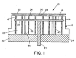
- Electrostatic chuck 10 can be, for example, of Coulombic type or of Johnson-Rahbek type, with the latter being preferred.
- Electrostatic chuck 10 includes chuck body 12 and, within chuck body 12, electrode 14.
- Electrode 14 can be a foil, a plate, a perforated foil or a perforated plate, a mesh, a screen printed layer or can have some other configuration that is suitable for incorporation into electrostatic chucks. Electrode 14 can be used as a chucking electrode, a plasma generating electrode or both. If the electrode operates as a chucking electrode only, a preferred thickness of the electrode is in a range of between about 10 ⁇ m (micrometers or microns) and about 50 ⁇ m Generally, a plasma generating electrode is thick enough to withstand the radio frequency (RF) applied to it. The preferred thickness of a plasma generating electrode ranges from about 50 ⁇ m to about 1 mm (millimeters).
- RF radio frequency
- a suitable of a mesh electrode has a wire diameter of about 125 ⁇ m and a mesh spacing of 19.6 wires per cm (50 wires per inch).
- electrode 14 is a flat film electrode such as described in U.S. Provisional Patent Application 60/169,859 , Electrostatic Chucks with Flat Film Electrode, filed December 9, 1999. Monoplolar as well as bipolar electrode configurations, as known in the art, can be employed.
- Electrode 14 is fabricated from a suitable metal or from a combination of metals or alloy.
- electrode 14 includes molybdenum (Mo), tungsten (W) or combinations of molybdenum and tungsten.
- Mo, W or Mo-W electrode includes additional metals, such as nickel and cobalt or other components such as sintering activators.
- suitable metals for fabricating of electrode 14 include, but are not limited to, tantalum, platinum, hafnium, rhodium, vanadium and alloys thereof.
- the electrode material is graphite.
- Chuck body 12 includes dielectric layer 16, at upper side 18 of electrode 14, and substrate 20, at lower side 22 of electrode 14.
- electrode 14 is completely and integrally embedded within chuck body 12.
- electrode 14 is sandwiched between dielectric layer 16 and substrate 20.
- a joint or seam (not shown) binds dielectric layer 16 to substrate 20.
- a joint or seam that does not allow ambient atmosphere to interact with electrode 14 is preferred.
- the joint or seam is formed by employing a suitable brazing material.
- the brazing material employed to form the join or seam also functions as electrode 14. Alternatively, there is no joint or seam between dielectric layer 16 and substrate 20.
- the thickness of dielectric layer 16 ranges from about 10 ⁇ m to about 5mm. In another embodiment, the dielectric resistivity of dielectric layer 16 is greater than 10 13 ohm•cm, at the operating temperature of the chuck, which is particularly suitable in the case of a Coulombic-type chuck. In yet another embodiment, the dielectric resistivity of dielectric layer 16 ranges from about 10 8 to about 10 13 ohm•cm, at the operating temperature of the chuck, which is particularly suitable for a Johnson-Rahbek-type electrostatic chuck.
- dielectric layer 16 and/or substrate 20 include but are not limited to aluminum oxide (Al 2 O 3 ), aluminum oxide-titanium oxide (Al 2 O 3 -TiO 2 ), aluminum nitride (AlN), silicon nitride (Si 3 N 4 ), silicon carbide (SiC), boron nitride (BN), yttrium oxide or yttria (Y 2 O 3) , yttrium aluminate (for example, Y 3 Al 5 O 12 , YAlO 3 , Al 2 Y 4 O 9 ) and any combination thereof. AlN is preferred.
- chuck body 12 has an uniform chemical composition.
- chuck body 12 can be constructed from different materials; for example, the chemical composition of substrate 20 can differ from that of dielectric layer 16.
- Chuck body 12, dielectric layer 16 and/or substrate 20 also can include additional components, for example, sintering aids, bonding agents and other materials, known in the art.
- additional components include but are not limited to yttrium oxide (Y 2 O 3 ), calcium salts and oxides, for instance, calcium fluoride or CaF 2 , calcium chloride or CaCl 2 , calcium oxide or CaO, calcium carbonate or CaCO 3 , calcium nitrate or Ca(NO 3 ) 2 , chromium oxide (Cr 2 O 3 ), silica (SiO 2 ), boron nitride (BN) and any combination(s) thereof, as well as secondary phases, formed by reaction(s) between the ceramic material and the additional component(s), such as, for example, compounds including yttrium aluminum and oxygen, for example, Y 3 Al 5 O 12 , YAlO 3 , Al 2 Y 4 O 9 or combinations thereof.
- Y 2 O 3 yttrium oxide
- CaF 2 calcium
- dielectric layer 16 and/or substrate 20 can also include Al 2 O 3 , an oxynitride of aluminum, (for example AlON), Y 2 O 3 , CaF 2 CaCl 2 , CaO, CaCO 3 , Ca(NO 3 ) 2 , Cr 2 O 3 , SiO 2 , BN, Y 3 Al 5 O 12 , YAlO 3 , Al 2 Y 4 O 9 or combinations thereof.
- electrostatic chuck 10 can further include a heating element (not shown).
- a heating element not shown.
- One suitable arrangement of an electrostatic chuck which includes an embedded heating element is described in U.S. Patent Application 09/457,968 , Electrostatic Chuck, Susceptor and Method for Fabrication , filed on December 9, 1999,.
- Electrostatic chuck 10 has back surface 24 and chucking surface 26.
- chucking surface 26 includes protrusions 28 and channels 30.
- a surface pattern such as one including, for example, protruding dimples or ridges significantly reduces contact area between work-piece 32 and chucking surface 26, and allows heat transfer fluid to circulate beneath work-piece 32.
- chucking surface 26 can be coated, for example, for enhanced erosion and/or corrosion resistance.
- Coatings which can be applied onto chucking surface 26 include but are not limited to pyrolytic BN, yttria, an yttrium aluminate, aluminum trfluoride (AlF 3 ), diamond and diamond-like coatings, such as, for example, coatings applied by chemical vapor deposition (CVD) methods. Thin coatings are preferred, such as, for example, coatings ranging from about 1 micrometer ( ⁇ m) to about 100 ⁇ m in thickness.
- electrical connector 34 is attached to electrode 14 through means known in the art.
- electrical connector 34 can be brazed to electrode 14.
- a contact plug (not shown) is co-sintered to the electrode and joined to electrical connector 34. Contacts and/or electrical connectors that have good electrical conductivity, low RF impedence and are easily joined to electrode 14 are preferred.
- electrical connector 34 includes, at electrode 14, an electrical contact such as described in U.S. Patent Application 09/457,968 , Electrostatic Chuck Susceptor and Method for Fabrication , filed on December 9,1999 .
- Electrostatic chuck 10 also includes one or more lift pin holes 36 which accommodate lift pins typically employed to raise or lower work-piece 32 from chucking surface 26.
- lift pin holes 36 extend from back surface 24, through substrate 20, electrode 14, dielectric layer 16, to chucking surface 26.
- Electrode 14 has apertures which align with lift pin holes 36 but, preferably, are larger in diameter, thereby preventing the lift pins from contacting electrode 14.
- the number of lift pin holes 36 generally depends on the chuck design and its application.
- Electrostatic chuck 10 includes at least one conduit 38 which provides fluid communication between back surface 24 and chucking surface 26.
- conduit 38 extends from back surface 24, through substrate 20, electrode 14, dielectric layer 16, to chucking surface 26.
- electrode 14 has apertures which align with conduit 38 and, preferably, are larger in diameter, thereby preventing heat transfer gas flowing through conduit 38 from contacting electrode 14.
- the cross section of conduit 38 can have, for example, a circular, elliptical, ring-like shape or any other suitable shape.
- Either or both the shape or dimensions of the cross section of conduit 38 can be essentially constant throughout the thickness of electrostatic chuck 10. Alternatively, either or both the shape or dimensions of conduit 38 can vary between back surface 24 and chucking surface 26.
- Conduit 38 includes porous zone or region 40 which is integrated within chuck body 12.
- Porous region 40 can include a ceramic material such as, for example, AlN, Si 3 N 4 , Al 2 O 3 , Al 2 O 3 -TiO 2 , SiC.
- porous region 40 can further include one or more components such as, for example, additives, sintering aids or bonding agents.
- additional components include but are not limited to yttrium oxide (Y 2 O 3 ), calcium salts and oxides, for instance, calcium fluoride or CaF 2 , calcium chloride or CaCl 2 , calcium oxide or CaO, calcium carbonate or CaCO 3 , calcium nitrate or Ca(NO 3 ) 2 , chromium oxide (Cr 2 O 3 ), silica (SiO 2 ), boron nitride (BN) and any combination(s) thereof.
- Porous region 40 also can include reaction products, also referred to herein as secondary phases, formed by reaction(s) between the ceramic material and the additional component(s).
- porous region 40 includes AlN and an yttrium aluminate, such as, for example, Y 3 Al 5 O 12 , YAlO 3 , Al 2 Y 4 O 9 or combinations thereof. Porous region 40 can also include Al 2 O 3 or an oxynitride of aluminum, for example AlON. In another embodiment, porous region 40 includes AlN and Y 2 O 3 , CaF 2 , CaCl 2 , CaO, CaCO 3 , Ca(NO 3 ) 2 , Cr 2 O 3 , SiO 2 , BN or a combination(s) thereof. Porous region 40 can be fabricated from the same material employed to fabricate dielectric layer 16 or chuck body 12.
- porous region 40 has a porosity sufficient to allow a required gas flow to the chucking surface. Pores small enough to restrict plasma penetration into conduit 38 are preferred. Also preferred are pores which do not form a direct line of sight between the backside (side resting on electrostatic chuck 10) of workpiece 32, electrode 14 and cathode pedestal 42, which supports electrostatic chuck 10.
- the porosity and average pore size employed can vary depending on the chuck design and/or application of a particular chuck.
- the porosity of porous region 40 is in a range of between about 10% and about 60% and preferably in a range of between about 30% and about 50%.
- average pore size ranges from about 5 ⁇ m to about 500 ⁇ m, with preferred pores having an average size between from about 20 ⁇ m to about 100 ⁇ m.
- Porous region 40 is integrated or integrally bonded to chuck body 12.
- the terms "integrated” or “integrally bonded” mean that porous region 40 is part of chuck body 12.
- the interface between porous region 40 and chuck body 12 does not present cracks, seams, joints or other defects.
- porous region 40 is diffusion-bonded to surrounding chuck body 12.
- porous region 40 is chemically bonded to surrounding chuck body 12.
- Porous region 40 can also be sintered into surrounding chuck body 12.
- a plurality of conduits 38 which include porous region 40, are employed.
- the number, dimensions and arrangement of porous regions 40 can depend, for example, upon the design and/or application of a particular chuck. Porous regions 40 can but need not have the same porosity.
- most or all of chuck body 12 is porous.
- most or all of dielectric layer 16 is porous.
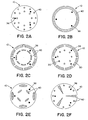
- all porous regions 40 have the same shape. In another embodiment all porous regions 40 have the same dimensions. In still another embodiment electrostatic chuck 10 includes porous regions having different shapes. Some suitable cross sectional shapes of porous region 40 are shown in Figure 3 .
- porous region 40 is a porous plug, such as, for example, a cylindrical porous plug.
- the number, dimensions and arrangement of the porous plugs can depend, for example, upon the design and/or application of a particular chuck.
- the diameter of the porous plug ranges from about 0.5 millimeter (mm) to about 20 mm.
- electrostatic chuck 10 has between about 1 and about 100 porous plugs, and preferably between about 20 and about 50 porous plugs.
- electrostatic chuck 10 includes porous regions 40 which are concentric rings.
- the surface area at the chucking surface of one ring is greater than the surface area of another ring.
- the porosity of the ring having the greater surface area is less than that of the ring which has the smaller surface area.
- porous region 40 prevents the formation of a direct line of sight from workpiece 32 (in particular from the side of workpiece 32 which rests on electrostatic chuck 10) to electrode 14 and to cathode pedestal 42.
- porous region 40 integrally bonded to chuck body 12, extends from back surface 24 to chucking surface 26, as shown in Figure 1 .
- porous region 40 also integrally bonded to chuck body 12, only partially extends through conduit 38.
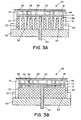
- FIG. 3A is a cross sectional view of one embodiment of the invention, - represented as electrostatic chuck 44.
- Electrostatic chuck 44 includes conduit 38 to provide fluid communication between back surface 24, and chucking surface 26.
- Conduit 38 includes porous region 40, at back surface 24. Porous region 40 is in the shape of a porous plug and is integrally bonded to substrate 20. Porous region 40 partially extends from back surface 24 through conduit 38, towards, but not all the way to, chucking surface 26.
- Conduit 38 also includes opening 46, which does not include porous material and which extends from porous zone 40 to chucking surface 26. Porosity and other pore-related properties, the numbers and volume of porous regions 40, the diameter and number of openings 46 are factors which can vary from one chuck design to another, depending on the application and the desired volume flow of heat transfer fluid.
- Electrostatic chuck 48 includes porous region 40 at back surface 24. Porous region 40 is integrally bonded to substrate 20. It partially extends from back surface 24, some distance towards, but not all the way to, chucking surface 26.
- the cross section of porous region 40 can be, for example, elliptical, a ring or another suitable shape, such as a shape illustrated in Figure 2 .
- Electrostatic chuck 48 also includes openings 46, which do not include porous material and extend from porous region 40 to chucking surface 26. As discussed above, porosity and other pore-related properties, numbers and volume of porous regions 40, the diameter and number of openings 46 are factors which can vary from one chuck design to another, depending on the application and the desired volume flow of heat transfer fluid.
- the porous region is at the chucking surface and is integrally bonded to the dielectric layer of the chuck body.
- the porous region extends from the chucking surface through the chuck body towards, but not all the way to, the back surface.
- the porous region extends from the chucking surface through the electrode.
- One or more openings for directing heat transfer fluid extend from the porous region to the back surface.
- Porous regions which partially extend through the conduit between the back surface and the chucking surface and are integrally bonded to the chuck body can be placed in other zones within the conduit, for example, away from both the back surface and the chucking surface.
- Electrostatic chucks which combine porous regions which extend from back surface to the chucking surface and porous regions which only partially extend through the conduit also can be fabricated.
- a heat transfer fluid is directed, from back surface 24, through porous region 40 to chucking surface 26.
- a heat transfer fluid is directed from back surface 24, through porous region(s) 40, openings 46 to chucking surface 26.
- Heat transfer fluid exits at chucking surface 26 and, optionally, circulates though channels 22, thereby modifying the temperature of work-piece 32.
- Heat transfer fluid can be supplied from a source, not shown in the figures and directed to porous region 40, for example, through an opening in cathode pedestal 42. Heat transfer fluid can be supplied to porous region 40 via tubings, pipings, regulators, fittings, valves, plenum reservoir(s), any combinations thereof, or other suitable means known in the art.
- heat transfer fluids include, but are not limited to, helium, argon, or other inert gases, as well as gases which are inert in the particular operation, environment and conditions in which electrostatic chuck is employed, and mixtures thereof.
- the heat transfer fluid can be at a temperature suitable in effecting the desired modification of the work-piece temperature.
- Heat transfer fluid within a desired temperature range can be supplied to chuck 10 as known in the art, for example by heating of cooling the heat transfer fluid in a heat exchanger, or by using cryogenic fluids.
- the pressure of heat transfer fluid supplied to conduit 38 can be controlled as known in the art.
- the heat transfer fluid is supplied at a pressure such that the flow of heat transfer fluid exiting at chucking surface 26 does not interfere with the electrostatic forces exerted upon work-piece 32 and the operation of the electrostatic chuck.
- design parameters such as, for example, the porosity, pore size and volume of the porous regions can be chosen to obtain a desired volume flow.
- a desired gas conductance is dependent on the size of pores and the amount of porosity in porous region 40.
- Gas conductance is the volume of gas allowed to flow through at a given pressure.
- the porosity of a large porous region can be adjusted, for example, to yield an equivalent gas conductance of a small porous plug.
- the invention also is related to methods of producing an electrostatic chuck.
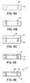
- first portion 50 of a green chuck body includes recess 52.
- green refers to the pre-densified state of a ceramic precursor.
- the green chuck body can be a compacted (for example cold-pressed), non-densified body of a precursor, such as, for example a powder or slurry, which upon densification will form a ceramic body.
- first portion 50 is formed by compacting AlN powder.
- Suitable materials which can be employed include, but are not limited to, AlN, Si 3 N 4 , Al 2 O 3 , Al 2 O 3 -TiO 2 or SiC, BN, Y 2 O 3 , yttrium aluminates or any combination thereof.
- Plug 54 is positioned into recess 52, as shown in Figure 4B .
- Plug 54 can have any suitable shape, as discussed above. More than one plug 54 can be incorporated in the green body. Optionally, plug 54 can be surrounded by a dense sleeve, which is co-sintered around plug 54.
- Plug 54 is in a green form which can be compacted into recess 52.
- plug 54 in its green form can be a powder compacted into recess 52 or can be a cold pressed green pellet molded to fit into recess 52.
- plug 54 With plug 54 being its green form, allowance is made for its shrinkage during densification along with shrinkage of first green portion 50, as is known in the art.
- Plug 54 becomes porous upon densification or as a result of another processing step (for example during heat treatment or soaking) or by treatment with an agent as further described below.
- Suitable materials which can be employed to form the green form of plug 54 include, but are not limited to, AlN, Si 3 N 4 , Al 2 O 3 , Al 2 O 3 -TiO 2 , SiC. AlN, BN, Y 2 O 3 , yttrium aluminates or any combination thereof is preferred. The same material can be employed to form both the green body and the green form of plug 54.
- plug 54 in its green form, includes removable particles.
- Removable particles can be in the form of powders, beads, granules, spheres, chopped fibers, filaments or can have other suitable shapes. Particles having an uniform size, as known in the art, also can be employed. The amount, shape and particle sizes employed can be selected to result, upon the removal of the particles, in a porous region having a desired porosity and a desired pore size range as discussed above.
- Removable particles can include compounds which decompose or burn off at the temperatures employed in the manufacture of electrostatic chucks.
- removable particles can include organic compounds, polymers, metal complexes, organometallic compounds and other fugitive materials which decompose or burn off, for example during heat treating, soaking, sintering or hot pressing. Clean burning fugitive compounds, which do not cause undesirable emissions are preferred.
- Particularly preferred are polymers of acrylic or methacrylic acid, for example polymethylmethacrylate (PMMA).
- PMMA polymethylmethacrylate
- Polystyrene, polyethylene, acrylic resins, cellulose acetate, cured epoxy resins, polyimide resins are examples of other materials which can be included in the green body. Copolymers, ter-polymers as well as cross-linked modifications thereof also can be employed.
- the green form of plug 54 can include metal particles which can be removed, preferably after densification of the green body, by etching with a suitable chemical agent, for example, a mixture of HF and HNO 3 .
- a suitable chemical agent for example, a mixture of HF and HNO 3 .
- a continuous phase of a metal such as, for example, molybdenum (Mo), tungsten (W), rhodium (Rh), vanadium (V), niobium (Nb), hafnium (Hf) and other refractory metals or alloys thereof is employed.
- the green form of plug 54 also can include one or more additional components.
- the green form of plug 54 includes one or more components that serve as a bonding agent and/or as a sintering aid.
- additional components which can be included in the green are: Y 2 O 3 , CaF 2 , CaCl 2 , CaO, CaCO 3 , Ca(NO 3 ) 2 , Cr 2 O 3 , SiO 2 , BN, combinations thereof as well as other commonly used sintering aids.
- the additional component(s) form a liquid phase during sintering.
- the green form of plug 54 does not include a sintering and/or bonding agents.
- the green form of plug 54 also can be formed from a coarse powder which, upon densification, results in a porous region such as described above.
- a sintering inhibitor such as magnesium oxide (MgO), silica (SiO 2 ), silicates, such as, for example, aluminum silicate or magnesium silicate, carbon (in excess of the carbon amount required to reduce oxygen) or another suitable sintering inhibitor can be added to a desired region in the green body.
- the sintering inhibitor prevents complete densification in that region and upon densification conditions, the incompletely densified region is porous.
- Electrode 14 is positioned onto first green portion 50 of the green chuck body.
- Electrode 14 can be, for example, a mesh electrode, in which case mesh openings can be arranged concentrically around plug 54.
- electrode 14 can be a screen printed layer, a foil or plate provided with apertures which align concentrically but are larger in diameter than plug 54, thereby preventing the electrode material from contacting plug 54. If a dense sleeve, co-sintered around plug 54, is employed, hole perforation into electrode 14 is simplified since the dense sleeve serves as a barrier between plug 54 and electrode 14.
- Second portion 56 of a green chuck body is overlaid onto electrode 14.
- Second portion 56 includes a dielectric material. Ceramic precursors and additional components which are suitable in forming first portion 50 also can be employed in forming second portion 56. In a preferred embodiment, both first portion 50 and second portion 56 have the same composition.
- the resulting assembly is densified, for example, by sintering to obtain a dense structure having porous region 40 (in this case a porous plug), which is integrally bonded to chuck body 12 as shown in Figure 4D .
- Sintering can be in the absence of pressure (pressure less sintering) or by hot pressing.
- the sintering temperature can depend on the particular materials employed in the fabrication of the electrostatic chuck. In the case of an AlN compacted powder, the sintering temperature ranges from about 1500°C to about 2000°C. If sintering is conducted under pressure, the pressure can range from about 10 MPa (mega Pascal) to about 40 MPa.
- a dense sleeve co-sintered to the plug is employed, as described above, thereby preventing a possible collapse of the plug during hot pressing.
- Sintering can be under an inert atmosphere, as described in U.S. Patent Application No. 09/458,278 , titled High-Purity Low-Resistivity Electrostatic Chuck , filed on December 9, 1999. Heat treating steps, as known in the art can also be employed.
- porous region 40 are exposed at back surface 24 and at chucking surface 26, for example by machining, thereby forming electrostatic chuck 10, shown in Figure 4E .
- a method for obtaining an electrostatic chuck having a partially extended porous region or plug, for example at back surface 26, includes the steps shown in Figures 4A and 4B , as described above.
- First portion 50 of a green chuck body, including plug 54 are then densified, for example, by a method described above, after which they are overlayed by electrode 14 and second portion 56.
- the resulting assembly is exposed to conditions such, for example, as hot pressing or pressureless sintering, which result in densification of second portion 56.
- An opening extending from chucking surface 26 to porous region 40 is formed, for example by machining.
- a pin inserted into the green form of second portion 56, prior to its densification, can be removed, leaving behind the desired opening.
- the end of porous plug 40 is exposed at back surface 24 as described above.
- Another method of producing an electrostatic chuck includes integrating a porous plug into a dense chuck body.
- the chuck body and the porous plug can be fabricated separately, for example, from materials and by methods described above.
- the porous plug itself is fabricated by densifying a green form of a plug which includes fugitive materials.
- the plug can include or can be coated with a bonding agent, such as the bonding agents described above.
- a bonding agent such as the bonding agents described above.
- AlN chuck bodies and AlN porous plug Y 2 O 3 , Y 3 Al 5 O 12 , YAlO 3 , Al 2 Y 4 O 9 and combinations thereof are preferred.
- Al 2 O 3 or oxynitrides of Al also can be employed as bonding agents. Bonding agents amounts, with respect to the porous region, generally range from about 0.5 weight % to about 10 weight %. If a high purity electrostatic chuck is desired, minimum amounts of bonding agents necessary to effect bonding of the plug to
- Integration of the porous plug into the surrounding chuck body can be accomplished by heating to a temperature sufficient to effect diffusion bonding between the porous plug and the chuck body.
- the temperature can be high enough to soften or to liquify the bonding agent thereby joining the porous plug to the chuck body.
- Example 1 Fabrication of Porous Plugs Via a Fugitive Based Technique
- PMMA polymethylmethacrylate
- the PMMA was in the form of spherical beads approximately 50 ⁇ m in diameter.
- the mixture was then cold pressed at 210 MPa to form several "green" cylindrical plugs approximately 12.5 mm (0.5 in) in diameter and 22 mm (0.86 in) long.
- a second batch of "green" porous plug precursors was fabricated in identical fashion except that the weight fraction of the 50 ⁇ m PMMA was 30%.
- a third batch of "green" porous plug precursors was fabricated in identical fashion except that the size of the PMMA beads was approximately 100 ⁇ m (-120/+170 mesh) and the weight fraction of PMMA used was 30%.
- each batch of green plug precursors was placed in an oven and heated in air to 600°C at a heating rate of 0.4°C/min, held for one hour at 600°C and cooled back to room temperature. These plugs were then sintered at 1850°C for one hour in nitrogen to obtain sintered porous plugs.
- A1N porous plugs from Example 3 were machined such that their outer diameter matched the diameter of the holes in the AlN body.
- One porous plug was then inserted into each hole in the A1N body.
- the assembly was heated in a furnace to 1850°C, soaked at 1850°C for an hour, and subsequently cooled to room temperature. Upon inspection, it was discovered that all three porous plugs had fused to the A1N body. Air was passed through the porous plugs to verify that the plugs had adequate conductance.
- the same experiment was repeated with another identical assembly of porous plugs in an A1N body with the dual purpose of joining the plugs to the A1N body as well as adjusting the resistivity of the A1N body.
- the assembly was heat treated at 1750°C for 4 hours in argon and then cooled to room temperature.
- the porous plugs had bonded to the main A1N body and had adequate (gas) conductance.
- the resistivity of the A1N body was 5x10 10 ohm•cm (measured at room temperature and an electric field of 500 V/mm).
Landscapes
- Engineering & Computer Science (AREA)
- Microelectronics & Electronic Packaging (AREA)
- Condensed Matter Physics & Semiconductors (AREA)
- General Physics & Mathematics (AREA)
- Manufacturing & Machinery (AREA)
- Computer Hardware Design (AREA)
- Physics & Mathematics (AREA)
- Power Engineering (AREA)
- Container, Conveyance, Adherence, Positioning, Of Wafer (AREA)
- Porous Artificial Stone Or Porous Ceramic Products (AREA)
- Chemical Vapour Deposition (AREA)
- Drying Of Semiconductors (AREA)
- Photoreceptors In Electrophotography (AREA)
- Holding Or Fastening Of Disk On Rotational Shaft (AREA)
Applications Claiming Priority (3)
| Application Number | Priority Date | Filing Date | Title |
|---|---|---|---|
| US09/655,324 US6606234B1 (en) | 2000-09-05 | 2000-09-05 | Electrostatic chuck and method for forming an electrostatic chuck having porous regions for fluid flow |
| US655324 | 2000-09-05 | ||
| PCT/US2001/024135 WO2002021590A2 (en) | 2000-09-05 | 2001-08-01 | Electrostatic chuck with porous regions |
Publications (2)
| Publication Number | Publication Date |
|---|---|
| EP1316110A2 EP1316110A2 (en) | 2003-06-04 |
| EP1316110B1 true EP1316110B1 (en) | 2008-12-10 |
Family
ID=24628428
Family Applications (1)
| Application Number | Title | Priority Date | Filing Date |
|---|---|---|---|
| EP01955029A Expired - Lifetime EP1316110B1 (en) | 2000-09-05 | 2001-08-01 | Electrostatic chuck with porous regions |
Country Status (9)
| Country | Link |
|---|---|
| US (1) | US6606234B1 (enExample) |
| EP (1) | EP1316110B1 (enExample) |
| JP (1) | JP4959905B2 (enExample) |
| KR (1) | KR100557695B1 (enExample) |
| AT (1) | ATE417358T1 (enExample) |
| AU (1) | AU2001277237A1 (enExample) |
| DE (1) | DE60136940D1 (enExample) |
| TW (1) | TW526521B (enExample) |
| WO (1) | WO2002021590A2 (enExample) |
Cited By (2)
| Publication number | Priority date | Publication date | Assignee | Title |
|---|---|---|---|---|
| US20200273736A1 (en) * | 2017-09-29 | 2020-08-27 | Sumitomo Osaka Cement Co., Ltd. | Electrostatic chuck device |
| WO2023150006A1 (en) * | 2022-02-03 | 2023-08-10 | Applied Materials, Inc. | Electrostatic chuck with porous plug |
Families Citing this family (62)
| Publication number | Priority date | Publication date | Assignee | Title |
|---|---|---|---|---|
| US7988999B2 (en) * | 2000-12-07 | 2011-08-02 | Nycomed Gmbh | Pharmaceutical preparation in the form of a paste comprising an acid-labile active ingredient |
| TWI234417B (en) * | 2001-07-10 | 2005-06-11 | Tokyo Electron Ltd | Plasma procesor and plasma processing method |
| US6490145B1 (en) * | 2001-07-18 | 2002-12-03 | Applied Materials, Inc. | Substrate support pedestal |
| TW561515B (en) * | 2001-11-30 | 2003-11-11 | Tokyo Electron Ltd | Processing device, and gas discharge suppressing member |
| US20030219986A1 (en) * | 2002-05-22 | 2003-11-27 | Applied Materials, Inc. | Substrate carrier for processing substrates |
| KR100457833B1 (ko) * | 2002-05-24 | 2004-11-18 | 주성엔지니어링(주) | 플라즈마 식각 장치 |
| JP4095842B2 (ja) * | 2002-06-26 | 2008-06-04 | 日本特殊陶業株式会社 | 静電チャック |
| JP2004306191A (ja) * | 2003-04-07 | 2004-11-04 | Seiko Epson Corp | テーブル装置、成膜装置、光学素子、半導体素子及び電子機器 |
| DE102004060625A1 (de) * | 2004-12-16 | 2006-06-29 | Siltronic Ag | Beschichtete Halbleiterscheibe und Verfahren und Vorrichtung zur Herstellung der Halbleiterscheibe |
| US7235139B2 (en) * | 2003-10-28 | 2007-06-26 | Veeco Instruments Inc. | Wafer carrier for growing GaN wafers |
| US7245357B2 (en) * | 2003-12-15 | 2007-07-17 | Asml Netherlands B.V. | Lithographic apparatus and device manufacturing method |
| US7220497B2 (en) * | 2003-12-18 | 2007-05-22 | Lam Research Corporation | Yttria-coated ceramic components of semiconductor material processing apparatuses and methods of manufacturing the components |
| US20060023395A1 (en) * | 2004-07-30 | 2006-02-02 | Taiwan Semiconductor Manufacturing Co., Ltd. | Systems and methods for temperature control of semiconductor wafers |
| US7544251B2 (en) * | 2004-10-07 | 2009-06-09 | Applied Materials, Inc. | Method and apparatus for controlling temperature of a substrate |
| JP4350695B2 (ja) * | 2004-12-01 | 2009-10-21 | 株式会社フューチャービジョン | 処理装置 |
| US7731798B2 (en) * | 2004-12-01 | 2010-06-08 | Ultratech, Inc. | Heated chuck for laser thermal processing |
| WO2006088448A1 (en) * | 2005-02-16 | 2006-08-24 | Veeco Instruments Inc. | Wafer carrier for growing gan wafers |
| US20090016941A1 (en) * | 2006-01-11 | 2009-01-15 | Ngk Insulators Ltd. | Electrode Device For Plasma Discharge |
| US20080009417A1 (en) * | 2006-07-05 | 2008-01-10 | General Electric Company | Coating composition, article, and associated method |
| WO2008082978A2 (en) * | 2006-12-26 | 2008-07-10 | Saint-Gobain Ceramics & Plastics, Inc. | Electrostatic chuck and method of forming |
| US7848076B2 (en) * | 2007-07-31 | 2010-12-07 | Applied Materials, Inc. | Method and apparatus for providing an electrostatic chuck with reduced plasma penetration and arcing |
| US9202736B2 (en) * | 2007-07-31 | 2015-12-01 | Applied Materials, Inc. | Method for refurbishing an electrostatic chuck with reduced plasma penetration and arcing |
| US8108981B2 (en) * | 2007-07-31 | 2012-02-07 | Applied Materials, Inc. | Method of making an electrostatic chuck with reduced plasma penetration and arcing |
| JP2008172255A (ja) * | 2008-01-25 | 2008-07-24 | Ngk Spark Plug Co Ltd | 静電チャック |
| US8681472B2 (en) * | 2008-06-20 | 2014-03-25 | Varian Semiconductor Equipment Associates, Inc. | Platen ground pin for connecting substrate to ground |
| US8218284B2 (en) * | 2008-07-24 | 2012-07-10 | Hermes-Microvision, Inc. | Apparatus for increasing electric conductivity to a semiconductor wafer substrate when exposure to electron beam |
| US8094428B2 (en) * | 2008-10-27 | 2012-01-10 | Hermes-Microvision, Inc. | Wafer grounding methodology |
| US20100107974A1 (en) * | 2008-11-06 | 2010-05-06 | Asm America, Inc. | Substrate holder with varying density |
| US9218997B2 (en) * | 2008-11-06 | 2015-12-22 | Applied Materials, Inc. | Electrostatic chuck having reduced arcing |
| US20100177454A1 (en) * | 2009-01-09 | 2010-07-15 | Component Re-Engineering Company, Inc. | Electrostatic chuck with dielectric inserts |
| US20110024049A1 (en) | 2009-07-30 | 2011-02-03 | c/o Lam Research Corporation | Light-up prevention in electrostatic chucks |
| US9338871B2 (en) * | 2010-01-29 | 2016-05-10 | Applied Materials, Inc. | Feedforward temperature control for plasma processing apparatus |
| US8916793B2 (en) * | 2010-06-08 | 2014-12-23 | Applied Materials, Inc. | Temperature control in plasma processing apparatus using pulsed heat transfer fluid flow |
| US8880227B2 (en) | 2010-05-27 | 2014-11-04 | Applied Materials, Inc. | Component temperature control by coolant flow control and heater duty cycle control |
| US8608852B2 (en) | 2010-06-11 | 2013-12-17 | Applied Materials, Inc. | Temperature controlled plasma processing chamber component with zone dependent thermal efficiencies |
| US9728429B2 (en) | 2010-07-27 | 2017-08-08 | Lam Research Corporation | Parasitic plasma prevention in plasma processing chambers |
| US8906164B2 (en) | 2010-08-05 | 2014-12-09 | Lam Research Corporation | Methods for stabilizing contact surfaces of electrostatic chucks |
| JP5458050B2 (ja) | 2011-03-30 | 2014-04-02 | 日本碍子株式会社 | 静電チャックの製法 |
| US10274270B2 (en) | 2011-10-27 | 2019-04-30 | Applied Materials, Inc. | Dual zone common catch heat exchanger/chiller |
| JP5956379B2 (ja) * | 2012-04-27 | 2016-07-27 | 日本碍子株式会社 | 半導体製造装置用部材 |
| KR102032744B1 (ko) | 2012-09-05 | 2019-11-11 | 삼성디스플레이 주식회사 | 기판 고정장치 및 이의 제조방법 |
| CN104748574A (zh) * | 2013-12-27 | 2015-07-01 | 北京思能达节能电气股份有限公司 | 一种用于监测自焙电极焙烧状态的系统和方法 |
| US9976211B2 (en) * | 2014-04-25 | 2018-05-22 | Applied Materials, Inc. | Plasma erosion resistant thin film coating for high temperature application |
| CN107004626B (zh) * | 2014-11-20 | 2019-02-05 | 住友大阪水泥股份有限公司 | 静电卡盘装置 |
| WO2016135565A1 (en) | 2015-02-23 | 2016-09-01 | M Cubed Technologies, Inc. | Film electrode for electrostatic chuck |
| JP6722518B2 (ja) | 2016-06-09 | 2020-07-15 | 新光電気工業株式会社 | 焼結体及びその製造方法と静電チャック |
| JP6854600B2 (ja) * | 2016-07-15 | 2021-04-07 | 東京エレクトロン株式会社 | プラズマエッチング方法、プラズマエッチング装置、および基板載置台 |
| US20180025931A1 (en) * | 2016-07-22 | 2018-01-25 | Applied Materials, Inc. | Processed wafer as top plate of a workpiece carrier in semiconductor and mechanical processing |
| US10975469B2 (en) * | 2017-03-17 | 2021-04-13 | Applied Materials, Inc. | Plasma resistant coating of porous body by atomic layer deposition |
| JP2019029384A (ja) * | 2017-07-25 | 2019-02-21 | 新光電気工業株式会社 | セラミックス混合物、多孔質体及びその製造方法、静電チャック及びその製造方法、基板固定装置 |
| KR102039802B1 (ko) * | 2017-12-19 | 2019-11-26 | 한국세라믹기술원 | 정전척용 세라믹 본체 |
| US10411380B1 (en) | 2018-05-24 | 2019-09-10 | Microsoft Technology Licensing, Llc | Connectors with liquid metal and gas permeable plugs |
| US11456161B2 (en) * | 2018-06-04 | 2022-09-27 | Applied Materials, Inc. | Substrate support pedestal |
| CN111668148B (zh) * | 2019-03-05 | 2024-09-03 | Toto株式会社 | 静电吸盘及处理装置 |
| JP7345379B2 (ja) * | 2019-12-06 | 2023-09-15 | 株式会社ディスコ | ゲッタリング性評価装置 |
| JP7634644B2 (ja) * | 2021-02-17 | 2025-02-21 | アプライド マテリアルズ インコーポレイテッド | 多孔性プラグ結合 |
| CN119404302A (zh) | 2022-07-07 | 2025-02-07 | 日本特殊陶业株式会社 | 保持装置 |
| CN119968703A (zh) * | 2022-09-30 | 2025-05-09 | 应用材料公司 | 用于氩气输送的大直径多孔栓塞及两阶段软性夹持方法 |
| US20240158308A1 (en) * | 2022-11-11 | 2024-05-16 | Applied Materials, Inc. | Monolithic substrate support having porous features and methods of forming the same |
| KR20250126049A (ko) * | 2022-12-21 | 2025-08-22 | 도쿄엘렉트론가부시키가이샤 | 기판 처리 장치 및 정전 척 |
| KR102795089B1 (ko) * | 2022-12-28 | 2025-04-15 | 세메스 주식회사 | 서셉터 및 그 제조방법 |
| KR20250068704A (ko) | 2023-04-19 | 2025-05-16 | 니혼도꾸슈도교 가부시키가이샤 | 유지 장치 |
Family Cites Families (14)
| Publication number | Priority date | Publication date | Assignee | Title |
|---|---|---|---|---|
| JPS62155517A (ja) * | 1985-12-27 | 1987-07-10 | Canon Inc | パターン描画装置及び方法 |
| US5542559A (en) | 1993-02-16 | 1996-08-06 | Tokyo Electron Kabushiki Kaisha | Plasma treatment apparatus |
| US5792562A (en) | 1995-01-12 | 1998-08-11 | Applied Materials, Inc. | Electrostatic chuck with polymeric impregnation and method of making |
| JPH0917770A (ja) * | 1995-06-28 | 1997-01-17 | Sony Corp | プラズマ処理方法およびこれに用いるプラズマ装置 |
| JP3457477B2 (ja) | 1995-09-06 | 2003-10-20 | 日本碍子株式会社 | 静電チャック |
| US6399143B1 (en) | 1996-04-09 | 2002-06-04 | Delsys Pharmaceutical Corporation | Method for clamping and electrostatically coating a substrate |
| JPH09289201A (ja) * | 1996-04-23 | 1997-11-04 | Tokyo Electron Ltd | プラズマ処理装置 |
| US6022807A (en) * | 1996-04-24 | 2000-02-08 | Micro Processing Technology, Inc. | Method for fabricating an integrated circuit |
| US5720818A (en) * | 1996-04-26 | 1998-02-24 | Applied Materials, Inc. | Conduits for flow of heat transfer fluid to the surface of an electrostatic chuck |
| US5835334A (en) | 1996-09-30 | 1998-11-10 | Lam Research | Variable high temperature chuck for high density plasma chemical vapor deposition |
| US6004752A (en) * | 1997-07-29 | 1999-12-21 | Sarnoff Corporation | Solid support with attached molecules |
| US6045753A (en) * | 1997-07-29 | 2000-04-04 | Sarnoff Corporation | Deposited reagents for chemical processes |
| JPH11260899A (ja) * | 1998-03-10 | 1999-09-24 | Nippon Steel Corp | 静電チャック |
| JP2001308075A (ja) * | 2000-04-26 | 2001-11-02 | Toshiba Ceramics Co Ltd | ウェーハ支持体 |
-
2000
- 2000-09-05 US US09/655,324 patent/US6606234B1/en not_active Expired - Lifetime
-
2001
- 2001-08-01 WO PCT/US2001/024135 patent/WO2002021590A2/en not_active Ceased
- 2001-08-01 EP EP01955029A patent/EP1316110B1/en not_active Expired - Lifetime
- 2001-08-01 DE DE60136940T patent/DE60136940D1/de not_active Expired - Fee Related
- 2001-08-01 AU AU2001277237A patent/AU2001277237A1/en not_active Abandoned
- 2001-08-01 AT AT01955029T patent/ATE417358T1/de not_active IP Right Cessation
- 2001-08-01 KR KR1020037003208A patent/KR100557695B1/ko not_active Expired - Lifetime
- 2001-08-01 JP JP2002525911A patent/JP4959905B2/ja not_active Expired - Lifetime
- 2001-08-07 TW TW090119231A patent/TW526521B/zh not_active IP Right Cessation
Cited By (5)
| Publication number | Priority date | Publication date | Assignee | Title |
|---|---|---|---|---|
| US20200273736A1 (en) * | 2017-09-29 | 2020-08-27 | Sumitomo Osaka Cement Co., Ltd. | Electrostatic chuck device |
| US11664261B2 (en) * | 2017-09-29 | 2023-05-30 | Sumitomo Osaka Cement Co., Ltd. | Electrostatic chuck device |
| WO2023150006A1 (en) * | 2022-02-03 | 2023-08-10 | Applied Materials, Inc. | Electrostatic chuck with porous plug |
| US11794296B2 (en) | 2022-02-03 | 2023-10-24 | Applied Materials, Inc. | Electrostatic chuck with porous plug |
| US12162111B2 (en) | 2022-02-03 | 2024-12-10 | Applied Materials, Inc. | Electrostatic chuck with porous plug |
Also Published As
| Publication number | Publication date |
|---|---|
| JP2004508728A (ja) | 2004-03-18 |
| JP4959905B2 (ja) | 2012-06-27 |
| DE60136940D1 (de) | 2009-01-22 |
| WO2002021590A2 (en) | 2002-03-14 |
| AU2001277237A1 (en) | 2002-03-22 |
| KR20030031177A (ko) | 2003-04-18 |
| WO2002021590A3 (en) | 2002-08-01 |
| TW526521B (en) | 2003-04-01 |
| KR100557695B1 (ko) | 2006-03-07 |
| EP1316110A2 (en) | 2003-06-04 |
| ATE417358T1 (de) | 2008-12-15 |
| US6606234B1 (en) | 2003-08-12 |
Similar Documents
| Publication | Publication Date | Title |
|---|---|---|
| EP1316110B1 (en) | Electrostatic chuck with porous regions | |
| JP4467453B2 (ja) | セラミックス部材及びその製造方法 | |
| KR100645349B1 (ko) | 금속부재 내장 소결체의 제조 방법 | |
| JP3654142B2 (ja) | 半導体製造装置用ガスシャワー体 | |
| KR100420456B1 (ko) | 반도체 제조 장치용 웨이퍼 지지체와 그 제조 방법 및반도체 제조 장치 | |
| US9340462B2 (en) | Transient liquid phase, pressureless joining of aluminum nitride components | |
| KR100438881B1 (ko) | 반도체 제조 장치용 웨이퍼 보유체 및 그것을 이용한반도체 제조 장치 | |
| KR20080025012A (ko) | 정전 척 및 그 제조 방법 | |
| KR20040030803A (ko) | 세라믹 접합체 및 그 접합방법, 세라믹 구조체 | |
| CN103681437A (zh) | 静电吸盘 | |
| TWI413438B (zh) | 半導體製造裝置用之保持單元、及裝載有該保持單元之半導體製造裝置 | |
| CN103681433A (zh) | 静电吸盘 | |
| KR100911485B1 (ko) | 전극내장형 서셉터 및 그 제조방법 | |
| JP4387563B2 (ja) | サセプタ及びサセプタの製造方法 | |
| JP2008098626A (ja) | 静電チャック及びその製造方法 | |
| US20230140614A1 (en) | Multi-layer composite ceramic plate and manufacturing method thereof | |
| JP2001308165A (ja) | サセプタ及びその製造方法 | |
| JP2001007189A (ja) | 静電チャック及びその製造方法 | |
| KR100918714B1 (ko) | 전극 내장형 서셉터 및 그 제조 방법 | |
| JP2006128205A (ja) | ウェハ支持部材 | |
| JP7240232B2 (ja) | 保持装置 | |
| KR20230096465A (ko) | 세라믹 서셉터의 제조 방법 | |
| JP2005175508A (ja) | 半導体製造装置用ガスシャワー体 | |
| JP2024104939A (ja) | セラミックスサセプタ | |
| JP2003168724A (ja) | 半導体製造・検査装置用セラミック基板およびその製造方法 |
Legal Events
| Date | Code | Title | Description |
|---|---|---|---|
| PUAI | Public reference made under article 153(3) epc to a published international application that has entered the european phase |
Free format text: ORIGINAL CODE: 0009012 |
|
| 17P | Request for examination filed |
Effective date: 20030227 |
|
| AK | Designated contracting states |
Designated state(s): AT BE CH CY DE DK ES FI FR GB GR IE IT LI LU MC NL PT SE TR |
|
| AX | Request for extension of the european patent |
Extension state: AL LT LV MK RO SI |
|
| RIN1 | Information on inventor provided before grant (corrected) |
Inventor name: DIVAKAR, RAMESH |
|
| 17Q | First examination report despatched |
Effective date: 20050801 |
|
| GRAP | Despatch of communication of intention to grant a patent |
Free format text: ORIGINAL CODE: EPIDOSNIGR1 |
|
| GRAS | Grant fee paid |
Free format text: ORIGINAL CODE: EPIDOSNIGR3 |
|
| GRAA | (expected) grant |
Free format text: ORIGINAL CODE: 0009210 |
|
| AK | Designated contracting states |
Kind code of ref document: B1 Designated state(s): AT BE CH CY DE DK ES FI FR GB GR IE IT LI LU MC NL PT SE TR |
|
| REG | Reference to a national code |
Ref country code: GB Ref legal event code: FG4D |
|
| REG | Reference to a national code |
Ref country code: CH Ref legal event code: EP |
|
| REG | Reference to a national code |
Ref country code: IE Ref legal event code: FG4D |
|
| REF | Corresponds to: |
Ref document number: 60136940 Country of ref document: DE Date of ref document: 20090122 Kind code of ref document: P |
|
| PG25 | Lapsed in a contracting state [announced via postgrant information from national office to epo] |
Ref country code: FI Free format text: LAPSE BECAUSE OF FAILURE TO SUBMIT A TRANSLATION OF THE DESCRIPTION OR TO PAY THE FEE WITHIN THE PRESCRIBED TIME-LIMIT Effective date: 20081210 Ref country code: NL Free format text: LAPSE BECAUSE OF FAILURE TO SUBMIT A TRANSLATION OF THE DESCRIPTION OR TO PAY THE FEE WITHIN THE PRESCRIBED TIME-LIMIT Effective date: 20081210 |
|
| NLV1 | Nl: lapsed or annulled due to failure to fulfill the requirements of art. 29p and 29m of the patents act | ||
| PG25 | Lapsed in a contracting state [announced via postgrant information from national office to epo] |
Ref country code: ES Free format text: LAPSE BECAUSE OF FAILURE TO SUBMIT A TRANSLATION OF THE DESCRIPTION OR TO PAY THE FEE WITHIN THE PRESCRIBED TIME-LIMIT Effective date: 20090321 Ref country code: BE Free format text: LAPSE BECAUSE OF FAILURE TO SUBMIT A TRANSLATION OF THE DESCRIPTION OR TO PAY THE FEE WITHIN THE PRESCRIBED TIME-LIMIT Effective date: 20081210 |
|
| PG25 | Lapsed in a contracting state [announced via postgrant information from national office to epo] |
Ref country code: SE Free format text: LAPSE BECAUSE OF FAILURE TO SUBMIT A TRANSLATION OF THE DESCRIPTION OR TO PAY THE FEE WITHIN THE PRESCRIBED TIME-LIMIT Effective date: 20090310 Ref country code: AT Free format text: LAPSE BECAUSE OF FAILURE TO SUBMIT A TRANSLATION OF THE DESCRIPTION OR TO PAY THE FEE WITHIN THE PRESCRIBED TIME-LIMIT Effective date: 20081210 Ref country code: PT Free format text: LAPSE BECAUSE OF FAILURE TO SUBMIT A TRANSLATION OF THE DESCRIPTION OR TO PAY THE FEE WITHIN THE PRESCRIBED TIME-LIMIT Effective date: 20090511 |
|
| PLBE | No opposition filed within time limit |
Free format text: ORIGINAL CODE: 0009261 |
|
| STAA | Information on the status of an ep patent application or granted ep patent |
Free format text: STATUS: NO OPPOSITION FILED WITHIN TIME LIMIT |
|
| PG25 | Lapsed in a contracting state [announced via postgrant information from national office to epo] |
Ref country code: DK Free format text: LAPSE BECAUSE OF FAILURE TO SUBMIT A TRANSLATION OF THE DESCRIPTION OR TO PAY THE FEE WITHIN THE PRESCRIBED TIME-LIMIT Effective date: 20081210 |
|
| 26N | No opposition filed |
Effective date: 20090911 |
|
| PG25 | Lapsed in a contracting state [announced via postgrant information from national office to epo] |
Ref country code: MC Free format text: LAPSE BECAUSE OF NON-PAYMENT OF DUE FEES Effective date: 20090831 |
|
| REG | Reference to a national code |
Ref country code: CH Ref legal event code: PL |
|
| GBPC | Gb: european patent ceased through non-payment of renewal fee |
Effective date: 20090801 |
|
| PG25 | Lapsed in a contracting state [announced via postgrant information from national office to epo] |
Ref country code: LI Free format text: LAPSE BECAUSE OF NON-PAYMENT OF DUE FEES Effective date: 20090831 Ref country code: CH Free format text: LAPSE BECAUSE OF NON-PAYMENT OF DUE FEES Effective date: 20090831 |
|
| REG | Reference to a national code |
Ref country code: FR Ref legal event code: ST Effective date: 20100430 |
|
| REG | Reference to a national code |
Ref country code: IE Ref legal event code: MM4A |
|
| PG25 | Lapsed in a contracting state [announced via postgrant information from national office to epo] |
Ref country code: FR Free format text: LAPSE BECAUSE OF NON-PAYMENT OF DUE FEES Effective date: 20090831 Ref country code: DE Free format text: LAPSE BECAUSE OF NON-PAYMENT OF DUE FEES Effective date: 20100302 Ref country code: IE Free format text: LAPSE BECAUSE OF NON-PAYMENT OF DUE FEES Effective date: 20090801 |
|
| PG25 | Lapsed in a contracting state [announced via postgrant information from national office to epo] |
Ref country code: GR Free format text: LAPSE BECAUSE OF FAILURE TO SUBMIT A TRANSLATION OF THE DESCRIPTION OR TO PAY THE FEE WITHIN THE PRESCRIBED TIME-LIMIT Effective date: 20090311 |
|
| PG25 | Lapsed in a contracting state [announced via postgrant information from national office to epo] |
Ref country code: GB Free format text: LAPSE BECAUSE OF NON-PAYMENT OF DUE FEES Effective date: 20090801 |
|
| PG25 | Lapsed in a contracting state [announced via postgrant information from national office to epo] |
Ref country code: IT Free format text: LAPSE BECAUSE OF FAILURE TO SUBMIT A TRANSLATION OF THE DESCRIPTION OR TO PAY THE FEE WITHIN THE PRESCRIBED TIME-LIMIT Effective date: 20081210 |
|
| PG25 | Lapsed in a contracting state [announced via postgrant information from national office to epo] |
Ref country code: LU Free format text: LAPSE BECAUSE OF NON-PAYMENT OF DUE FEES Effective date: 20090801 |
|
| PG25 | Lapsed in a contracting state [announced via postgrant information from national office to epo] |
Ref country code: TR Free format text: LAPSE BECAUSE OF FAILURE TO SUBMIT A TRANSLATION OF THE DESCRIPTION OR TO PAY THE FEE WITHIN THE PRESCRIBED TIME-LIMIT Effective date: 20081210 |
|
| PG25 | Lapsed in a contracting state [announced via postgrant information from national office to epo] |
Ref country code: CY Free format text: LAPSE BECAUSE OF FAILURE TO SUBMIT A TRANSLATION OF THE DESCRIPTION OR TO PAY THE FEE WITHIN THE PRESCRIBED TIME-LIMIT Effective date: 20081210 |