EP1309094A1 - Unite de commande de la puissance d'emission - Google Patents
Unite de commande de la puissance d'emission Download PDFInfo
- Publication number
- EP1309094A1 EP1309094A1 EP01948052A EP01948052A EP1309094A1 EP 1309094 A1 EP1309094 A1 EP 1309094A1 EP 01948052 A EP01948052 A EP 01948052A EP 01948052 A EP01948052 A EP 01948052A EP 1309094 A1 EP1309094 A1 EP 1309094A1
- Authority
- EP
- European Patent Office
- Prior art keywords
- transmission power
- control
- section
- voltage
- feedback
- Prior art date
- Legal status (The legal status is an assumption and is not a legal conclusion. Google has not performed a legal analysis and makes no representation as to the accuracy of the status listed.)
- Withdrawn
Links
- 230000005540 biological transmission Effects 0.000 title claims abstract description 300
- 238000001514 detection method Methods 0.000 claims abstract description 195
- 230000008859 change Effects 0.000 claims description 16
- 230000015572 biosynthetic process Effects 0.000 claims description 5
- 238000003786 synthesis reaction Methods 0.000 claims description 5
- 238000012986 modification Methods 0.000 description 43
- 230000004048 modification Effects 0.000 description 43
- 238000010586 diagram Methods 0.000 description 15
- 230000007423 decrease Effects 0.000 description 9
- 239000000470 constituent Substances 0.000 description 8
- 230000004044 response Effects 0.000 description 5
- 238000013459 approach Methods 0.000 description 3
- 238000010420 art technique Methods 0.000 description 2
- 230000006378 damage Effects 0.000 description 2
- 238000005259 measurement Methods 0.000 description 2
- 238000004891 communication Methods 0.000 description 1
- 238000013461 design Methods 0.000 description 1
- 230000009467 reduction Effects 0.000 description 1
- 230000007704 transition Effects 0.000 description 1
Images


Classifications
-
- H—ELECTRICITY
- H04—ELECTRIC COMMUNICATION TECHNIQUE
- H04W—WIRELESS COMMUNICATION NETWORKS
- H04W52/00—Power management, e.g. TPC [Transmission Power Control], power saving or power classes
- H04W52/04—TPC
- H04W52/52—TPC using AGC [Automatic Gain Control] circuits or amplifiers
-
- H—ELECTRICITY
- H03—ELECTRONIC CIRCUITRY
- H03G—CONTROL OF AMPLIFICATION
- H03G3/00—Gain control in amplifiers or frequency changers
- H03G3/20—Automatic control
- H03G3/30—Automatic control in amplifiers having semiconductor devices
- H03G3/3036—Automatic control in amplifiers having semiconductor devices in high-frequency amplifiers or in frequency-changers
- H03G3/3042—Automatic control in amplifiers having semiconductor devices in high-frequency amplifiers or in frequency-changers in modulators, frequency-changers, transmitters or power amplifiers
- H03G3/3047—Automatic control in amplifiers having semiconductor devices in high-frequency amplifiers or in frequency-changers in modulators, frequency-changers, transmitters or power amplifiers for intermittent signals, e.g. burst signals
-
- H—ELECTRICITY
- H04—ELECTRIC COMMUNICATION TECHNIQUE
- H04B—TRANSMISSION
- H04B1/00—Details of transmission systems, not covered by a single one of groups H04B3/00 - H04B13/00; Details of transmission systems not characterised by the medium used for transmission
- H04B1/02—Transmitters
- H04B1/04—Circuits
- H04B2001/0408—Circuits with power amplifiers
- H04B2001/0416—Circuits with power amplifiers having gain or transmission power control
Definitions
- the present invention relates to a transmission power control circuit, and more particularly, to a transmission power control circuit controlling a transmission power of a transmitting wave using a detector.
- a feedback control using a detector was performed to control a transmission power of a transmitting wave output.
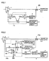
- a transmission power control circuit 10 included: a variable gain amplifier 1; a distributor 2; a detecting circuit 3; a reference voltage generating circuit 4; and a power control section 5.
- Variable gain amplifier 1 amplifies a transmission signal with a gain according to a given control voltage V C to generate a transmitting wave output.
- Distributor 2 takes out part of a transmission power P OUT of a transmitting wave output.
- Detecting circuit 3 detects part of the transmission power obtained by distributor 2 and generates a detection voltage V DET according to transmission power P OUT . That is, detection voltage V DET changes according to transmission power P OUT .
- Reference voltage generating circuit 4 generates a reference voltage V REF corresponding to a designated level of transmission power P OUT .
- Power control section 5 generates control voltage V C according to a negative-fed back voltage K 0 •V DET obtained by multiplying detection voltage V DEF from detecting circuit 3 by a detection voltage feed-back ratio K 0 , and to V REF from reference voltage generating circuit 4, based on the following equation (1).
- V C V REF -K 0 •V DET
- reference voltage generating circuit 4 includes a transmission power designating section 7; a control section 8; and D/A converter 9.
- Transmission power designated value P CMD indicating a designated level of a transmission power is converted to reference voltage V REF by control section 8 and D/A converter 9. That is, reference voltage V REF is set in correspondence to transmission power designated value P CMD .
- Power control section 5 includes: an operational amplifier 10; and resistance elements 11 and 12. Detection voltage V DET from detecting circuit 3 is transmitted to a node N0 corresponding to the inverted input terminal (- terminal) of operational amplifier 10 through resistance element 12. Reference voltage V REF from D/A converter 9 is inputted to the non-inverting input terminal (+ terminal) of operational amplifier 10. Resistance element 11 is coupled between the inverted input terminal and the output terminal of operational amplifier 10. Therefore, detection voltage feed-back ratio K 0 shown in Fig. 28 is determined according to a ratio between resistance elements 11 and 12.
- detecting circuit 3 can output a detection voltage corresponding to a transmission power all over a dynamic range of transmission power P OUT .
- a dynamic range of transmission power is set wide, generally, it is rather difficult to broaden a measurable range of detecting circuit 3 than to broaden a dynamic range of a gain of variable gain amplifier 1.
- a detecting circuit tends to become complex and up-scaled, resulting in a high cost.
- It is an object of the present invention is to provide a transmission power control circuit capable of ensuring a wide dynamic range of transmission power using a general inexpensive detecting circuit having a simple architecture.
- a transmission power control circuit includes: a variable gain amplifier for amplifying a transmission signal with a gain according to a control voltage to output a transmitting wave; a distributing section for taking out part of the transmitting wave; a detecting section for detecting an output of said distributing section to generate a detection voltage corresponding to a transmission power of the transmitting wave; and a control section receiving an electrical signal indicating a designated level of the transmission power and the detection voltage to set the control voltage.
- the control section performs a changeover between a first control state setting the control voltage by close loop control according to the detection voltage negative-fed back, multiplied by a feedback ratio and a reference voltage corresponding to the designated level, and a second control state setting the control voltage by open loop control according to the designated level, according to a relationship between a measurable power range of the detecting section and the transmission power.
- the control section preferably performs the changeover between the first and second control states according to the detection voltage.
- control section preferably performs the changeover between the first and second control states according to a designated level of the transmission power.
- control section preferably includes: a first signal converting section converting a detection voltage to a first digital signal; a control computing section receiving a second digital signal indicating a designated level of a transmission power and the first signal to perform a digital computing for setting a control voltage based on one of the first and second control state, which is selected according to comparison between the first and second digital signals; and a second signal converting section converting an output of the control computing section to an analog signal to generate the control voltage.
- control section preferably includes: a feedback ratio adjusting section for gradually reducing a feedback ratio from a prescribed level as a transmission power comes closer to a non-measurable power range in a prescribed boundary range between a measurable power range and non-measurable power range of a detection section in the first control state.
- the feedback ratio adjusting section more preferably changes a feedback ratio according to a detection voltage.
- the feedback ratio adjusting section more preferably changes a feedback ratio according to a designated level of a transmission power.
- the control section more preferably further includes: a first signal converting section converting a detection voltage to a first digital signal; and a second signal converting section converting an output of the feedback ratio adjusting section to an analog signal to generate a control voltage.
- the feedback ratio adjusting section receives a second digital signal indicating a designated level of a transmission power and a first digital signal to perform a digital computing for setting a control voltage based on a feedback ratio set according to the second digital signal.
- the transmission power control circuit includes: a variable gain amplifier amplifying a transmission signal with a gain according to a control voltage to output a transmitting wave; a plurality of distributing sections for taking out part of the transmitting wave; and a plurality of detecting sections, provided corresponding to each of the plurality of distributing sections, respectively, and having different measurable power ranges.
- the plurality of detecting sections detect outputs of the corresponding distributing sections to generate a plurality of detection voltages according to a transmission power of the transmitting wave.
- the transmission power control circuit further includes: a control section receiving an electrical signal indicating a designated level of a transmission power and a plurality of detection voltages to set a control voltage.
- the control section includes: a feedback ratio control section setting a plurality of feedback ratios corresponding to the plurality of detection voltages, respectively, according to a relationship between the measurable power ranges of the plurality of detecting sections and a transmission power.
- the control section sets a control voltage according to close loop control based on a plurality of detection voltages negative-fed back multiplying each of the plurality of feedback ratios and a reference voltage corresponding to a designated level of a transmission power.
- the measurable power ranges of at least part of the plurality of detecting sections preferably share an overlapped range between any two and the feedback ratio control section, when the transmission power of a transmitting wave corresponds to an overlapped range, sets the feedback ratios so that the detecting voltages from the detecting circuits sharing the overlapped range are synthesized and negative-fed back.
- the feedback ratio control section when the transmission power of a transmitting wave corresponds to an overlapped region, sets a plurality of feedback ratios so that a synthesis ratio between the plurality of detecting voltages to be synthesized gradually change according to the transmission power.
- Such a transmission power control circuit can implement dose loop control with a detective voltage in order to ensure a dynamic range of a transmission power to be wide without increasing a measurable range of each of the plurality of detecting sections, that is by using a plurality of common inexpensive detecting sections. Furthermore, a discontinuous change in transmission power can be prevented in changeover between mainly used detecting circuits according to a relationship between a measurable range of each of the detecting circuits and a detection voltage.
- the feedback ratio adjusting section preferably sets a plurality of feedback ratios according to a plurality of detection voltages.
- the feedback ratio adjusting section preferably sets a plurality of feedback ratios according to a designated level of a transmission power.
- the control section preferably further includes: a first signal converting section for converting a plurality of detection voltages to a plurality of first digital signals; and a second signal converting section converting an output of the feedback ratio adjusting section to an analog signal to generate a control voltage.
- the feedback ratio adjusting section receives a second digital signal indicating a designated level of a transmission power and a plurality of first digital signals to perform a digital computing for setting a control voltage based on a plurality of feedback ratios set according to a plurality of second digital signals.
- the control section when a transmission power does not belong to any of the measurable power ranges of a plurality of detecting sections, preferably temporarily ceases close loop control and sets a control voltage based on open loop control corresponding to a designated level of a transmission power.
- Such a transmission control circuit can further control a transmission power based on open loop control of the transmission power at a designated level of transmission power in a range in which the transmission power does not correspond to any of measurable ranges of a plurality of detecting sections. Therefore, a transmission power can be stably controlled without setting relationships between a designated level of a transmission power and a reference voltage separately inside and outside a measurable range of a detecting circuit.
- such a transmission power control circuit can implement close loop control with a detective voltage in order to ensure a dynamic range of a transmission power to be wide without increasing a measurable range of each of the plurality of detecting sections, that is by using a plurality of common inexpensive detecting sections. Furthermore, a discontinuous change in transmission power can be prevented in changeover between mainly used detecting circuits according to a relationship between a measurable range of each of the detecting circuits and a detection voltage.
- the control section more preferably performs a changeover between close loop control and open loop control and setting of a plurality of feedback ratios in close loop control according to a plurality of detection voltages.
- the control section more preferably performs a changeover between close loop control and open loop control and setting of a plurality of feedback ratios in close loop control according to a designated level of a transmission power.
- the control section more preferably further includes: a first signal converting section converting a plurality of detection voltages to each of the plurality of first digital signals; and a second signal converting section converting an output of the feedback ratio adjusting section to an analog signal to generate a control voltage.
- the feedback ratio adjusting section receives a second digital signal indicating a designated level of a transmission power and a plurality of first digital signals to perform a digital computing for setting a control voltage using a plurality of feedback ratios set according to a plurality of second digital signals, based on one of open loop control and close loop control, which is selected according to comparison between first and second digital signals.
- a transmission power control circuit 100 includes: a variable gain amplifier 1, a distributor 2, a detecting circuit 3; a reference voltage generating circuit 4 and a power control section 110.
- variable gain amplifier 1 amplifies a transmitting wave with a gain according to a control voltage V C from power control section 110 to generate a transmitting wave output.
- Distributor 2 takes out part of a transmission power P OUT from the transmitting wave output.
- Detecting circuit 3 detects the part of a transmission power obtained by distributor 2 to generate a detection voltage V DET corresponding to transmission power P OUT .
- Reference voltage generating circuit 4 generates a reference voltage V REF according to a designated level of transmission power P OUT .
- a detection voltage feedback ratio K and control voltage feedback ratio K' are set in an interlocked manner according to a relationship between transmission power P OUT and a measurable range of detecting circuit 3.
- Power control section 110 generates a control voltage V C according to the following equation (2) based on reference voltage V REF , detection voltage V DET and control voltage V C .
- V C V REF - (K•V DET + K'•V C )
- control voltage V C is generated by open loop control based on reference voltage V REF .
- a relationship between a transmission power designated value P CMD and reference voltage V REF has been determined on a precondition that negative-feedback through detecting circuit 3 has been performed. Therefore, when transmission power Pour is outside a measurable range of a detecting circuit 3, transmission power P OUT of a transmitting wave output controlled based on reference voltage V REF produces large error from transmission power designated value P CMD if negative-feedback from detecting circuit 3 is simply cut off.
- control voltage V C is generated using a product of control voltage V C and control voltage feedback ratio K' as a substitute for the cut-off of the negative-feedback to generate control voltage V C .
- a transmission power control circuit 101a includes: variable gain amplifier 1, distributor 2; detecting circuit 3; reference voltage generating circuit 4 and a power control section 120a.
- Reference voltage generating circuit 4 similar to the architecture shown in Fig. 25, includes: transmission power designating section 7; control section 8 and D/A converter 9.
- Transmission power designating section 7 generates transmission power designated value P CMD indicating a designated level of a transmission power.
- Control section 8 generates a digital signal corresponding to a transmission power designated value P CMD from transmission power designating section 7.
- D/A converter 9 generates reference voltage V REF having an analog voltage corresponding to a digital signal from control section 8.
- Power control section 120a includes: a threshold voltage generating circuit 121, a comparator 122, inverter 123, control state changeover switches 124 and 125; an operational amplifier 126; and resistance elements R1 to R3.
- Threshold voltage generating circuit generating a threshold voltage V TH for determining whether or not transmission power P OUT is inside a measurable range of detecting circuit 3 based on detection voltage V DET .
- Comparator 122 compares threshold voltage V TH from threshold voltage generating circuit 121 and detection voltage V DET from detecting circuit 3 with each other.
- Reference voltage V REF from D/A converter 9 is inputted to the non-inverting input terminal of operational amplifier 126.
- Resistance element R1 is coupled between the inverted input terminal and the output terminal of operational amplifier 126.
- Control voltage V C generated at the output terminal of operational amplifier 126 is transmitted to variable gain amplifier 1.
- Control state changeover switch 124 and resistance element R2 are coupled in series between the inverted input terminal of operational amplifier 126 and detecting circuit 3.
- Control state changeover switch 125 and resistance element R3 are coupled in series between the inverted input terminal of operational amplifier 126 and ground voltage GND.
- Control state changeover switches 124 and 125 are complementarily turned on/off corresponding to an output of comparator 122. When it is determined that transmission power P OUT falls within a measurable range of detection circuit 3, that is when an output of comparator 122 is set at H level, control state changeover switch 124 is turned on, while control state changeover switch 125 is turned off.
- control state changeover switch 125 is turned on, while control state changeover switch 124 is turned off.
- Detection voltage V DET is not transmitted to the inverted input terminal of operational amplifier 126 and operation amplifier 126 operates as a non-inverting amplifier with reference voltage V REF from D/A converter as only one input. Therefore, control voltage V C is generated by an open loop control system only following to reference voltage V REF , that is transmission power designated value P CMD .
- power control section 120a changes setting of detection voltage feedback ratio K according to a level of detection voltage V DET . That is, power control section 120a, when detection voltage V DET is higher than threshold voltage V TH , determines that transmission power P OUT is within a measurable range of detecting circuit 3 to set detection voltage feedback ratio K to K 0 .
- Resistance values of resistance elements R1 and R2 shown in Fig. 2 are designed so as to attain a prescribed feedback ratio K 0 .
- power control section 120a when detection voltage V DET is lower than threshold voltage V TH , determines that transmission power Pour is outside a measurable range of detecting circuit 3 to set detection voltage feedback ratio K to 0. That is, negative-feedback of detection voltage V DET is temporarily ceased to perform open loop control.
- a resistance value of resistance element R3 shown in Fig. 2 is designed in consideration of a relationship between reference voltage V REF and transmission power P OUT in open loop control.
- open loop control and close loop control are changed over therebetween based on detection voltage V DET according to transmission power P OUT .
- approximate coincidence occurs between an ideal control response indicated with a dotted line and an actual transmission power indicated with a solid line because of negative-feedback of detection voltage V DET .
- a gain of variable gain amplifier 1 is set according to transmission power designated value P CMD .
- a dynamic range of transmission power can be ensured wide without increasing a measurable range of a detecting circuit, that is using a general inexpensive detecting circuit.
- a transmission power control circuit 101b according to a first modification of the first embodiment is different from transmission power control circuit 101a shown in Fig. 2 in comparison in that a power control section 120b is included as constituent instead of power control section 120a.
- Power control section 120b is different from the power control section 120a shown in Fig. 2 in comparison that threshold voltage generating circuit 121 and comparator 122 is omitted.
- control section 8 performs issuance of an on/off command of control state changeover switches 124 and 125, that is, a changeover command between open loop control and close loop control. Control section 8 issues an on/off command for control state changeover switches 124 and 125 according to transmission power designated value P CMD .
- power control section 120b when transmission power designated value P CMD is larger than a prescribed level P TH, determines that transmission power P OUT is within a measurable range of detecting circuit 3 to set detection voltage feedback ratio K to K 0 .
- control state changeover switch 124 is turned on and control state changeover switch 125 is turned off, in response to a command of control section 8.
- power control section 120b when transmission power designated value P CMD is lower than a prescribed level P TH , determines that transmission power P OUT is out of a measurable range of detecting circuit 3 to set detection voltage feedback ratio K to 0. In this case, control state changeover switch 125 is turned on and control state changeover switch 124 is turned off, in response to a command of control section 8.
- a determination on whether or not actual transmission power P OUT is within a measurable range of detecting circuit 3 is executed based not on actual detection voltage V DET but on transmission power designated value P CMD . Since the other part and operations therein of transmission power control circuit 101b are similar to transmission power control circuit 101a shown Fig. 2, none of descriptions thereof is repeated.
- a circuit determining a level of detection voltage V DET that is, threshold voltage generating circuit 121 and comparator 122 can be deleted, thereby enabling simplification of an architecture of power control section 120b.
- a transmission power control circuit 101c according to a second modification of the first embodiment is different from the transmission power control circuit 101a shown in Fig. 2 in comparison in that power control section 120c is included instead of power control section 120a. Furthermore, control section 8 and D/A converter 9 are not included and transmission power designated value P CMD from transmission power designating section 7 is given directly to power control section 120c as a digital signal as is.
- Power control section 120c includes an A/D converter 135; a control computing section 137; and a D/A converter 139.
- A/D converter 135 converts detection voltage V DET form detecting circuit 3 to a digital signal.
- Control computing section 137 receives a digital signal according to detection voltage V DET form detecting circuit 3 and transmission power designated value P CMD as a digital signal unchanged to perform a digital computing based on detection voltage feedback ratio K set similarly to Fig. 6. That is, control computing section 137 performs a control operation similar to power control section 110b constructed as an analog circuit. A result of the operation in control computing section 137 is converted to an analog voltage by D/A converter 139 and transmitted to variable gain amplifier 1 as control voltage V C .
- transmission power control similar to the first modification of the first embodiment can be realized by a digital computing.
- a transmission power control circuit In a transmission power control circuit according to the first embodiment, changeover is made between open loop control and close loop control according a result of determination on whether or not actual transmission power P OUT is inside a measurable range of a detecting circuit.
- a detection voltage feedback ratio changes stepwise in the vicinity of a changeover boundary region between open loop control and close loop control, there is a risk of a sudden change in transmission power P OUT in the vicinity. Therefore, in the second embodiment, description will be given of a control scheme preventing a sudden change in a transmission power in a changeover boundary region between open loop control and close loop control.
- a transmission power control circuit 102a according to the second embodiment is different from transmission power control circuit 101a according to the first embodiment shown in Fig. 2 in comparison in that power control section 140a is included as constituent instead of power control section 120a.
- Power control section 140a is different from power control section 120a shown in Fig. 2 in comparison in that feedback control circuit 142 is incorporated instead of threshold voltage generating circuit 121 and comparator 122; a variable resistor 144 instead of control state changeover switch 124 and resistance element R2; and a variable resistor 146 instead of control state changeover switch 125 and resistance element R3.
- Feedback ratio control circuit 142 controls resistance values of variable resistors 144 and 146 according to detection voltage V DET from detecting circuit 3.
- Variable resistor 144 is used as means adjusting detection voltage feedback ratio K.
- Variable resistor 146 is used as means adjusting control voltage feedback ratio K'.
- feedback ratio control circuit 142 sets a resistance value of variable resistor 144 to the maximum ( ⁇ , ideally).
- a non-inverting amplifier with reference voltage V REF as an input is constituted by control voltage feedback ratio K' according to resistance element R1 and a resistance value of variable resistor 144 to thereby perform open loop control of transmission power P OUT based on transmission power designated value P CMD .
- feedback ratio control circuit 142 adjusts resistance values of variable resistors 144 and 146 so that detection voltage feedback ratio K gradually changes.
- detection voltage feedback ratio K is set so that transmission power P OUT decreases toward outside a measurable range of detecting circuit.
- a feedback ratio transition section where detection voltage feedback ratio K gradually changes in a changeover boundary region between open loop control and close loop control to change over between close loop control and open loop; therefore, a sudden change in transmission power can be prevented in the changeover boundary region.
- a transmission power control circuit 102b according to a first modification of the second embodiment is different from transmission power control circuit 102a shown in Fig. 8 in comparison in that power control section 140b is included instead of power control section 140a.
- Power control section 140b is different from power control section 140ashown in Fig. 8 in that feedback ratio control circuit 142 is omitted.
- resistance values of variable resistors 144 and 146 are controlled by control section 8.
- Control section 8 sets resistance values of variable resistors 144 and 146 according to transmission power designated value P CMD from transmission power designating section 7.
- control section 8 sets a resistance value of variable resistor 146 to the maximum ( ⁇ , ideally).
- detection voltage feedback ratio K is set to K 0 based on a ratio between resistance element R2 and a resistance value of variable resistor 144 to perform close loop control by negative-feedback of detection voltage V DET .
- control section 8 set a resistance value of variable resistor 144 to the maximum ( ⁇ , ideally).
- a non-inverting amplifier with reference voltage V REF as an input is constituted by control voltage feedback ratio K' according to resistance element R1 and a resistance value of variable resistor 146 to thereby perform open loop control of transmission power Pour based on transmission power designated value P CMD .
- control section 8 adjusts resistance values of variable resistors 144 and 146 so that detection voltage feedback ratio K gradually changes.
- Detection voltage feedback ratio K is set similar to the second embodiment so that transmission power Pour decreases toward outside a measurable range of detecting circuit in a changeover boundary region.
- transmission power control circuit 102b in transmission power control circuit 102b according to the first modification of the second embodiment, whether actual transmission power P OUT is inside or outside a measurable range of detecting circuit 3 is determined not by detection voltage V DET but by transmission power designated value P CMD .
- a circuit feedback ratio control circuit 142 in Fig. 8) performing determination based on detection voltage V DET is not required any longer in the system; thereby enabling simple architecture of a power control section to be realized.
- variable resistors 144 and 146 each of whose resistance value changes in an analog fashion.
- variable resistors a type whose resistance value gradually changes stepwise may also used. In this case, detection voltage feedback ratio K in a changeover boundary region gradually changes stepwise.
- transmission power control circuit 102c according to the second modification of the second embodiment is different from transmission power control circuit 102a shown in Fig. 8 in comparison in that power control section 140c is incorporated instead of power control section 140a. Furthermore, control section 8 and D/A converter 9 are omitted and transmission power designating value P CMD from transmission power designating section 7 is given directly to power control section 140c as a digital signal as is.
- Power control section 140c includes: an A/D converter 135; a control computing section 147; and a D/A converter 139.
- Control computing section 147 receives a digital signal corresponding to detection voltage V DET from detecting circuit 3 and transmission power designated value P CMD as a digital signal unchanged to perform a digital computing based on detection voltage feedback ratio K set similarly to Fig. 12. That is, in control computing section 137, a control operation similar to power control section 140b as an analog circuit. A result of the operation of control computing section 137 is converted to an analog signal by D/A converter 139 and transmitted to variable gain amplifier 1 as control voltage V C .
- the architectures are shown that is designed so that a measurable range of detecting circuit 3 corresponds to a relative high range of transmission power P OUT , an architecture can be adopted in which a measurable range of detecting circuit 3 corresponds to a relative small range of transmission power P OUT and a correspondence between large/small of transmission power P OUT and setting of open loop control/close loop control is reversed.
- transmission power control circuit 103a according to the third embodiment is different from transmission power control circuit 101a according to the first embodiment shown in Fig. 2 in comparison in that there are a plurality of incorporated distributors 2a, 2b and 2c, a first detecting circuit 3a, a second detecting circuit 3b and a third detecting circuit 3c, having respective different measurable ranges.
- First detecting circuit 3a, second detecting circuit 3b and third detecting circuit 3c are provided corresponding to distributors 2a, 2b ad 2c, respectively.
- First detecting circuit 3a generates detection voltage V DET1 by detecting part of transmission power obtained by distributor 2a.
- Second detecting circuit 3b generates detection voltage V DET2 by detecting part of transmission power obtained by distributor 2b.
- Third detecting circuit 3c generates detection voltage V DET3 by detecting part of transmission power obtained by distributor 2c.
- Transmission power control circuit 103a according to the third embodiment is different from transmission power control circuit 101a shown in Fig. 2 in comparison in that power control section 150a is incorporated instead of power control section 120a.
- Power control section 150a includes: a feedback ratio control circuit 152; variable resistors 154, 156 and 158; resistance element R2; and an operational amplifier 126.
- Variable resistor 154 is disposed between first detecting circuit 3a and the non-inverting input terminal of operational amplifier 126 to transmit detection voltage V DET1 .
- Variable resistor 156 is disposed between second detecting circuit 3b and the non-inverting input terminal of operational amplifier 126 to transmit detection voltage V DET2 .
- Variable resistor 158 is disposed between third detecting circuit 3c and the non-inverting input terminal of operational amplifier 126 to transmit detection voltage V DET3 .
- Feedback ratio control circuit 152 sets resistance values of variable resistor 154, 156 and 158 based on detection voltages V DET1 , V DET2 and V DET3 .
- first detecting circuit 3a, second detecting circuit 3b and third detecting circuit 3c have respective different measurable ranges
- measurable ranges between any two detecting circuits adjacent to each other are set so as to overlap on each other.
- a measurable range of first detecting circuit 3a corresponds to a range of V DET1 ⁇ V TH2
- a measurable range of second detecting circuit 3b corresponds to a range of V TH1 ⁇ V DET2 ⁇ V TH4
- a measurable range of third detecting circuit 3c corresponds to a range of V DET3 > V TH3 .
- Established between threshold voltages are relations that V TH1 ⁇ V TH2 and V TH4 > V TH3 .
- Feedback ratio control circuit 152 sets resistance values of variable resistors 154, 156 and 158 so that detection voltage feedback ratios K 1 , K 2 and K 3 corresponding to respective detection voltages V DET1 , V DET2 and V DET3 change as shown in Figs. 14A to 14C according to a detection voltage.
- detection voltage V DET1 corresponds to a measurable range of first detecting circuit 3a, that is when V DET1 ⁇ V TH2
- feedback ratio K1 corresponding to detection voltage V DET1 is set to K 1 > 0.
- detection voltage feedback ratio K 1 changes so as to gradually decrease toward a non-measurable range of first detecting circuit 3a, that is as V DET1 approaches V TH2 .
- detection voltage feedback ratio K 1 is set to prescribed level K 0 .
- detection voltage feedback ratio K 1 is set to 0.
- a resistance value of variable resistor 154 is set to the maximum value ( ⁇ , ideally).
- feedback ratio K 2 corresponding to detection voltage V DET2 is set to K 2 > 0 when detection voltage V DET2 corresponds to a measurable range of second detecting circuit 3b, that is in a case of V TH1 ⁇ V DET2 ⁇ V TH4 .
- detection voltage feedback ratio K 2 changes so as to gradually decrease toward a non-measurable range of second detecting circuit 3b.
- detection voltage feedback ratio K 1 is set to prescribed level K 0 in the other range, that is in a range of V TH1 ⁇ V TH2 . Furthermore, still in the other range, that is in a range of V TH2 ⁇ V DET2 ⁇ V TH3 , detection voltage feedback ratio K 2 is set to prescribed level K 0 .
- detection voltage feedback ratio K 2 is set to 0.
- a resistance value of variable resistor 156 is set the maximum value ( ⁇ , ideally).
- feedback ratio K 3 corresponding detection voltage V DET3 is set to K 3 > 0, when detection voltage V DET3 corresponds to a measurable range of third detecting circuit 3c, that is in a case of V DET3 > V TH3 .
- detection voltage feedback ratio K 3 changes so as to gradually decrease toward a non-measurable range of third detecting circuit 3c, that is as V DET3 comes to closer to V TH3 .
- detection voltage feedback ratio K 3 is set to prescribed level K 0 .
- detection voltage feedback ratio K 3 is set to 0.
- a resistance value of variable resistor 158 is set to the maximum value ( ⁇ , ideally).
- detection voltage feedback ratios K 1 to K 3 are set so that detection voltages from two detecting circuits sharing the overlapped measurable ranges with each other are synthesized and negative-fed back.
- detection voltage feedback ratios K 1 to K 3 are set so that a synthetic ratio between synthesized detection voltages gradually changes according to a relationship between a detection voltage and a measurable range of a detecting circuit.
- close loop control with a detection voltage for ensuring a wide dynamic range of a transmission power can be implemented without increasing measurable ranges of respective detecting circuits, that is by use of a plurality of general inexpensive detecting circuits. Furthermore, a discontinuous change in transmission power can be prevented in changeover between mainly used detecting circuits according to a relationship between a measurable range of each detecting circuit and a detection voltage.
- transmission power control circuit 103b according to a first modification of the third embodiment is different from transmission power control circuit 103a according to of the third embodiment in comparison in that a power control section 150b is included instead of power control section 150a.
- Power control section 150b is different from power control section 150a shown in Fig. 14 in that feedback ratio control circuit 152 is omitted in architecture.
- resistance values of variable resistors 154, 156 and 158 are controlled by control section 8.
- Control section 8 sets resistance values of variable resistors 154, 156 and 158 according to transmission power designated value P CMD from transmission power designating section 7 so that detection voltage feedback ratios K 1 , K 2 and K 3 change according to a detection voltage as shown in Fig. 17A to 17C.
- threshold voltages P TH1 , P TH2 , P TH3 and P TH4 are determined correspondingly to measurable ranges of first detecting circuit 3a, second detecting circuit 3b and third detecting circuit 3c, respectively.
- feedback ratio K 1 corresponding to detection voltage V DET1 is set to K 1 > 0 when it is determined that transmission power designated value P CMD corresponds to a measurable range of fist detecting circuit 3a, that is in a case of P CMD ⁇ P TH2 .
- detection voltage feedback ratio K 1 changes so as to gradually decrease toward a non-measurable range of first detecting circuit 3a, that is as P CMD approaches P TH2 .
- detection voltage feedback ratio K 1 is set to prescribed level K 0 .
- detection voltage feedback ratio K 1 is set to 0.
- feedback ratio K 2 corresponding to detection voltage V DET2 is set to K 2 > 0, when it is determined that transmission power designated value P CMD corresponds to a measurable range of second detecting circuit 3b, that is, in a case of P TH1 ⁇ P CMD ⁇ P TH4 .
- detection voltage feedback ratio K 2 changes so as to gradually decrease toward a non-measurable range of second detecting circuit 3b.
- detection voltage feedback ratio K 2 is set to prescribed level K 0 .
- detection voltage feedback ratio K 2 is set to prescribed level 0.
- feedback ratio K 3 corresponding to detection voltage V DET3 is set to K 3 > 0, when it is determined that transmission power designated value P CMD corresponds to a measurable range of third detecting circuit 3c, that is, in a case of P CMD > P TH3 .
- detection voltage feedback ratio K 3 changes so as to gradually decrease toward a non-measurable range of third detecting circuit 3c, that is as P CMD approaches P TH3 .
- detection voltage feedback ratio K 3 is set to prescribed level K 0 .
- detection voltage feedback ratio K 3 is set to 0.
- transmission power control circuit 103b in transmission power control circuit 103b according to the first modification of the second embodiment, it is determined which is a detection circuit corresponding to actual transmission power Pour according to transmission power designating value P CMD .
- a circuit as a constituent feedback ratio control circuit 152 in Fig. 14
- variable resistors 154, 156 and 158 respective resistance values changing in an analog fashion
- the resistors each may be of a type having a resistance value that changes gradually stepwise.
- transmission power control circuit 103c according to a second modification of the third embodiment is different from transmission power control circuit 103a according to the third embodiment in comparison in that power control section 150c is included as a constituent instead of power control section 150a. Furthermore, control section 8 and D/A converter 9 are omitted in the architecture and transmission power designated value P CMD from transmission designating section 7 is given directly to power control section 150c as a digital signal as is.
- Power control section 150c has a first A/D converter 135a; a second A/D converter 135b; a third A/D converter 135c; a control computing section 157; and a D/A converter 139.
- First A/D converter 135a; second A/D converter 135b; and third A/D converter 135c are provided corresponding to first detecting circuit 3a, second detecting circuit 3b and third detecting circuit 3c, respectively and detection voltages V DET1 , V DET2 and V DET3 are converted to digital signals.
- Control computing section 157 receives a plurality of digital signals corresponding to respective detection voltages V DET1 , V DET2 and V DET3 and transmission power designated value P CMD as a digital signal unchanged digital to perform a digital computing based on detection voltage feedback ratios K 1 , K 2 and K 3 , set similarly to Figs 17A to 17C. That is, in control computing section 157, there is performed a control operation similar to power control section 150b. A result of the operation in control computing section 157 is converted to an analog signal by D/A converter 139 and transmitted to variable gain amplifier 1 as control voltage V C .
- detection voltages V DET1 , V DET2 and V DET3 are converted to respective digital signals and close loop control is realized based on a digital computing, thereby enabling realization of transmission power control similar to the first modification of the third embodiment.
- transmission power control obtained by combining an architecture in which a dynamic range covering a wide range of a transmission power using a plurality of detection circuits which is described in the third embodiment and an architecture in which changeover is made between dose loop control and open loop control which is described in the first embodiment.
- transmission power control circuit 104a according to the fourth embodiment is different from transmission power control circuit 101a according to the first embodiment in comparison in that there is included first detecting circuit 3a and second detecting circuit 3b, both having respectively different measurable ranges, and distributors 2a and 2b corresponding to first detecting circuit 3a and second detecting circuit 3b.
- transmission power control circuit 104a includes: power control section 160a instead of power control section 120a shown in Fig. 2.
- a measurable range of first detecting circuit 3a corresponds to a range of V TH1 ⁇ V DET1 ⁇ V TH4 of a detection voltage.
- a measurable range of second detecting circuit 3b corresponds to a range of V DET2 > V TH3 of a detection voltage.
- measurable ranges of first detecting circuit 3a and second detecting circuit 3b are designed so as to be V TH3 ⁇ V TH4 , that is so that parts of measurable ranges are overlapped on each other.
- power control section 160a includes: operational amplifier 126; resistance element R1; feedback ratio control circuit 162: and variable resistors 164, 166 and 168.
- Variable resistor 164 is coupled between first detecting circuit 3a and the inverted input terminal of operational amplifier 126 to transmit detection voltage V DET1 .
- Variable resistor 166 is coupled between second detecting circuit 3b and the inverted input terminal of operational amplifier 126 to transmit detection voltage V DET2 .
- Variable resistor 168 is coupled between the inverted input terminal of operational amplifier 126 and ground voltage GND. Resistance element R1 is connected between the inverted input terminal and the output terminal of operational amplifier 126.
- Feedback ratio control circuit 162 set resistance values of variable resistors 164, 166 and 168 based on detection voltages V DET1 and V DET2 .
- detection voltage feedback ratios K 1 and K 2 are both set to 0. That is, in this range, feedback ratio control circuit 162 sets resistance values of variable resistors 164 and 166 to the maximum value ( ⁇ , ideally).
- a non-inverting amplifier is constituted of operational amplifier 126, resistance element R1 and variable resistor 168, and control voltage V C is set based on open loop control. Resistance element R1 and a resistance value of variable resistor 168 is designed so that prescribed control voltage feedback ratio K' is obtained.
- variable resistor 168 In a range in which detection voltages V DET1 and V DET2 are higher than V TH1 , a resistance value of variable resistor 168 is set to the maximum value ( ⁇ , ideally) to change over from open loop control based on reference voltage V REF to close loop control with negative-feedback of a detection voltage.
- a resistance value variable resistor 164 is set so that feedback ratio K 1 gradually increases continuously.
- a resistance value of variable resistor 164 is set so that feedback ratio K 1 is prescribed detection voltage feedback ratio K 0 in a range of V TH2 ⁇ V DET1 ⁇ V TH3 of a detection voltage.
- a resistance value of variable resistor 166 is set to the maximum value ( ⁇ , ideally) so that feedback ratio K 2 is 0.
- resistance values of variable resistors 164 and 166 are set so that as a detection voltage goes higher, feedback ratio K 1 gradually decreases and in addition, feedback ratio K 2 gradually increases. That is, in a measurable range in which overlapping occurs between a plurality of detecting circuits, a detection voltage feedback ratio is set similarly to the third embodiment. Therefore, in this range, similar to the third embodiment, outputs of a plurality of detecting circuits are synthesized and negative-feedback is implemented. Furthermore, sudden changeover between synthesis ratios does not occur but a synthesis ratio gradually changes.
- control voltage V C that is a gain of variable gain amplifier 1
- V REF reference voltage
- implementation can be realized of close loop control with a detection voltage for ensuring a wide dynamic range of a transmission power without increasing a measurable range of each detecting circuit, that is by using a plurality of general inexpensive detecting circuits. Furthermore, a sudden change in transmission power in changeover between mainly used detecting circuits can be prevented according to a relationship between a measurable voltage of each detecting circuit and a detection voltage.
- transmission power control circuit 104b according to a first modification of the fourth embodiment is different from transmission power control circuit 104a shown in Fig. 18 in comparison in that a power control section 160b is included as constituent instead of power control section 160a.
- Power control section 160b is different from power control section 160a shown in Fig. 19 in that feedback control circuit 162 is omitted as constituent.
- resistance values of variable resistors 164, 166 and 168 are controlled by control section 8.
- Control section 8 sets resistance values of variable resistors 164, 166 and 168 according to transmission power designated value P CMD from transmission power designating section 7 so that detection voltage feedback ratios K 1 and K 2 change as shown in Figs. 20A and 20B according to a detection voltage.
- threshold voltages P TH1 , P TH2 , P TH3 and P TH4 are determined correspondingly to measurable ranges of detecting circuits 3a and 3b.
- a measurable range of detecting circuit 3a is determined correspondingly to a range of P TH1 ⁇ P CMD ⁇ P TH4 of transmission power designated value P CMD .
- a measurable range of detecting circuit 3b is determined correspondingly to a range of P CMD > P TH3 of transmission power designated value P CMD .
- Overlapped measurable ranges of detecting circuits 3a and 3b are determined according to a range of P TH3 ⁇ P CMD ⁇ P TH4 .
- Control section 8 sets detection voltage feedback ratios K 1 in K 2 not according to a detection voltage but according to transmission power designated value P CMD .
- Setting of detection voltage feedback ratios K 1 and K 2 by control section 8 corresponds to replacement of V TH1 , V TH2 , V TH3 and V TH4 with threshold voltages P TH1 , P TH2 , P TH3 and P TH4 .
- control section 8 in a range in which transmission power designated value P CMD is lower than P TH1 , sets detection voltage feedback ratios K 1 and K 2 to 0 and control voltage V C is set only based on open loop control based on reference voltage V REF .
- control circuit 8 in a range in which transmission power designated value P CMD is higher than P TH1 , sets a resistance value of variable resistor 168 to the maximum value ( ⁇ , ideally) and changes over from open loop control based on reference voltage V REF to dose loop control by negative-feedback of a destruction voltage.
- a resistance value of variable resistor 164 is set so that feedback ratio K 1 gradually increase.
- outputs of a plurality of detection circuits are synthesized and negative-feedback is performed. Moreover, a synthesis ratio gradually changes.
- transmission power control circuit 104b which is a detecting circuit corresponding to actual transmission power P OUT is determined according to transmission power designated value P CMD .
- P CMD transmission power designated value
- variable resistors 164, 166 and 168 While in the fourth embodiment and the first modification thereof as well, the architectures are shown in which there are used variable resistors 164, 166 and 168, resistance values all changing in an analog fashion, the variable resistors may be of types whose resistance values change gradually stepwise.
- a transmission power control circuit 104c according to a second modification of the fourth embodiment is different from transmission power control circuit 104a according to the fourth embodiment in comparison in that a power control section 160c is included as constituent instead of power control section 160a. Furthermore, control section 8 and D/A converter 9 are omitted and transmission power designating value P CMD from transmission power designating section 7 is given directly to power control section 160c as a digital signal as is.
- Power control section 160c has a first A/D converter 135a; a second A/D converter 135b; a control computing section 167; and a D/A converter 139.
- First A/D converter 135a and second A/D converter 135b are provided corresponding to first detecting circuit 3a and second detecting circuit 3b, respectively, to convert detection voltages V DET1 and V DET2 to respective digital signals.
- Control arithmetic logic section 167 receives digital signals corresponding to detection voltages V DET1 and V DET2 and transmission power designating value P CMD as an digital signal unchanged performs a digital computing based on detection voltage feedback ratios K 1 and K 2 similarly to Figs. 22A and 22B. That is, in control computing section 167, there are performed a control operation similar to power control section 160b constructed as an analog circuit. A result of the operation of control computing section 167 is converted to an analog signal by D/A converter 139 and transmitted as control voltage V C to variable gain amplifier 1.
- detection voltages V DET1 and V DET2 are converted to respective digital signals and close loop control is realized based on a digital computing, thereby enabling realization of transmission power control similar to the first modification of the fourth embodiment.
- the architectures are described in which there are included as constituent two detecting circuits having respective different measurable ranges, three or more detecting circuits can also be used. In this case, a pair of a distributor and a variable resistor is required to be provided corresponding to each detection circuit.
- a section applied with an open loop can be set corresponding to any power range.
- a transmission power control circuit according to the present invention can be applied to a wireless communication apparatus such as a portable telephone.
Landscapes
- Engineering & Computer Science (AREA)
- Computer Networks & Wireless Communication (AREA)
- Signal Processing (AREA)
- Transmitters (AREA)
Applications Claiming Priority (1)
| Application Number | Priority Date | Filing Date | Title |
|---|---|---|---|
| PCT/JP2001/006190 WO2003009481A1 (fr) | 2001-07-17 | 2001-07-17 | Unite de commande de la puissance d'emission |
Publications (1)
| Publication Number | Publication Date |
|---|---|
| EP1309094A1 true EP1309094A1 (fr) | 2003-05-07 |
Family
ID=11737557
Family Applications (1)
| Application Number | Title | Priority Date | Filing Date |
|---|---|---|---|
| EP01948052A Withdrawn EP1309094A1 (fr) | 2001-07-17 | 2001-07-17 | Unite de commande de la puissance d'emission |
Country Status (5)
| Country | Link |
|---|---|
| US (1) | US6788138B2 (fr) |
| EP (1) | EP1309094A1 (fr) |
| JP (1) | JPWO2003009481A1 (fr) |
| CN (1) | CN1459149A (fr) |
| WO (1) | WO2003009481A1 (fr) |
Cited By (10)
| Publication number | Priority date | Publication date | Assignee | Title |
|---|---|---|---|---|
| EP1460778A3 (fr) * | 2003-03-07 | 2006-01-11 | Ubinetics Limited | Contrôle de la puissance émise |
| EP1622262A1 (fr) * | 2004-07-29 | 2006-02-01 | Sony Ericsson Mobile Communications AB | Unité radiofréquence et procédé de commande de puissance utilisable dans un équipement de radio-communication |
| EP1628394A1 (fr) * | 2003-05-23 | 2006-02-22 | Matsushita Electric Industrial Co., Ltd. | Circuit de detection et procede d'ajustement dudit circuit |
| WO2006022650A1 (fr) | 2004-07-28 | 2006-03-02 | Applied Science & Technology, Inc. | Procedes et systemes de stabilisation d'un amplificateur |
| US7075366B2 (en) | 2003-07-18 | 2006-07-11 | Mks Instruments, Inc. | Methods and systems for stabilizing an amplifier |
| US7639015B2 (en) | 2003-07-18 | 2009-12-29 | Mks Instruments, Inc. | Methods and systems for stabilizing an amplifier |
| US8461842B2 (en) | 2003-07-18 | 2013-06-11 | Mks Instruments, Inc. | Methods and systems for stabilizing an amplifier |
| CN1856900B (zh) * | 2003-09-22 | 2013-06-26 | 摩托罗拉移动公司 | 在频率跳变应用中的放大器功率控制及方法 |
| US8606311B2 (en) | 2008-02-08 | 2013-12-10 | Skyworks Solutions, Inc. | Closed-loop adaptive power control for adjusting bandwidth in a mobile handset transmitter |
| EP2490330A3 (fr) * | 2004-07-28 | 2015-01-21 | Mks Instruments, Inc. | Procédés et systèmes de stabilisation d'un amplificateur |
Families Citing this family (23)
| Publication number | Priority date | Publication date | Assignee | Title |
|---|---|---|---|---|
| WO2004020582A2 (fr) * | 2002-08-15 | 2004-03-11 | Functional Genetics, Inc. | Genes mammiferes impliques dans la resistance a la rapamycine et la tumorigenese designes sous le nom de genes rapr6 |
| US7171171B1 (en) * | 2003-08-15 | 2007-01-30 | Rf Micro Devices, Inc. | GaAs RF signal detection circuit with operational amplifier |
| US7493133B2 (en) * | 2004-02-05 | 2009-02-17 | Qualcomm, Incorporated | Power control in ad-hoc wireless networks |
| US20050206447A1 (en) * | 2004-03-18 | 2005-09-22 | Ryo Yamazaki | Method to prevent saturation in power amplifier control loop |
| JP2005348312A (ja) * | 2004-06-07 | 2005-12-15 | Renesas Technology Corp | 高周波電力増幅用電子部品 |
| US20060025104A1 (en) * | 2004-07-29 | 2006-02-02 | Reed Byron M | Dynamic trim to mitigate transients |
| US7205842B2 (en) * | 2005-01-13 | 2007-04-17 | Telefonaktiebolaget Lm Ericsson (Publ) | Continuous alternating closed-open loop power control |
| JP2007116651A (ja) * | 2005-09-22 | 2007-05-10 | Renesas Technology Corp | 高周波電力増幅用電子部品および無線通信装置 |
| JP4676383B2 (ja) * | 2006-05-31 | 2011-04-27 | ルネサスエレクトロニクス株式会社 | 送信回路及びそれを用いた移動体通信用送信機 |
| US8744510B2 (en) * | 2007-03-13 | 2014-06-03 | Pranav Dayal | Power control method and apparatus for wireless communications |
| TWM349649U (en) * | 2008-09-10 | 2009-01-21 | Amazing Microelectronic Corp | Bias balancing circuit |
| US8315581B2 (en) * | 2008-09-18 | 2012-11-20 | Intel Mobile Communications GmbH | Transmitter with hybrid closed loop power control |
| US8422968B2 (en) * | 2009-06-03 | 2013-04-16 | Apple Inc. | Wireless electronic device with open-loop and closed-loop output power control |
| US8565699B1 (en) | 2009-09-23 | 2013-10-22 | Marvell International Ltd. | Setting of power amplifier control voltage |
| US8417198B1 (en) * | 2009-10-28 | 2013-04-09 | Marvell International Ltd. | Selection of closed-loop/open-loop power control in user equipment |
| US8260226B1 (en) | 2009-10-28 | 2012-09-04 | Marvell International Ltd. | High-accuracy transmit power control with high-efficiency power amplifier operation |
| JP2010179152A (ja) * | 2010-05-10 | 2010-08-19 | Mks Instruments Inc | 増幅器を安定化する方法およびシステム |
| CN102255608A (zh) * | 2011-01-11 | 2011-11-23 | 苏州英诺迅科技有限公司 | 一种大动态范围自动增益调节电路 |
| JP5963632B2 (ja) * | 2012-09-28 | 2016-08-03 | 株式会社ダイヘン | 高周波電源装置及びその制御方法 |
| US9100033B2 (en) * | 2013-12-20 | 2015-08-04 | Motorola Solutions, Inc. | Systems and methods for using a digital power amplifier controller (DPAC) having foward-loop correction and feedback-loop correction |
| CN110022598B (zh) * | 2018-01-08 | 2023-08-08 | 深圳市中兴微电子技术有限公司 | 一种功率控制方法、终端和计算机可读存储介质 |
| TWI768926B (zh) * | 2021-05-25 | 2022-06-21 | 瑞昱半導體股份有限公司 | 訊號強度指標電路與傳輸電路 |
| CN113541643B (zh) * | 2021-09-16 | 2021-12-07 | 深圳市鼎阳科技股份有限公司 | 用于信号发生器的功率控制装置、方法和信号发生器 |
Family Cites Families (16)
| Publication number | Priority date | Publication date | Assignee | Title |
|---|---|---|---|---|
| JP2876837B2 (ja) | 1991-08-20 | 1999-03-31 | 日本電気株式会社 | 検波回路 |
| JP2826003B2 (ja) * | 1991-11-29 | 1998-11-18 | 松下電器産業株式会社 | 送信出力制御回路 |
| JPH06169228A (ja) | 1992-11-27 | 1994-06-14 | Sanyo Electric Co Ltd | 送信電力制御装置 |
| US5452473A (en) * | 1994-02-28 | 1995-09-19 | Qualcomm Incorporated | Reverse link, transmit power correction and limitation in a radiotelephone system |
| JP3192323B2 (ja) | 1994-07-29 | 2001-07-23 | 沖電気工業株式会社 | 電力制御回路 |
| JPH08102682A (ja) | 1994-10-03 | 1996-04-16 | Matsushita Electric Ind Co Ltd | Apc回路 |
| JPH09121132A (ja) | 1995-10-24 | 1997-05-06 | Oki Electric Ind Co Ltd | 無線装置の送信電力制御回路 |
| JP2954024B2 (ja) | 1996-07-12 | 1999-09-27 | 埼玉日本電気株式会社 | 送信電力制御回路 |
| JPH10145160A (ja) | 1996-11-15 | 1998-05-29 | Oki Electric Ind Co Ltd | 自動出力制御回路 |
| JP3263017B2 (ja) | 1997-10-22 | 2002-03-04 | 三菱電機株式会社 | 検波回路およびそれを用いた送信装置ならびに受信装置 |
| WO2000001084A1 (fr) * | 1998-06-29 | 2000-01-06 | Nokia Networks Oy | Controle de puissance dans un emetteur a plusieurs porteuses |
| JP2000101456A (ja) | 1998-09-24 | 2000-04-07 | Fujitsu Ltd | 無線送信装置 |
| JP2000349657A (ja) | 1999-06-08 | 2000-12-15 | Nec Saitama Ltd | Rf検波回路 |
| JP2001016116A (ja) | 1999-07-02 | 2001-01-19 | Nec Corp | 携帯無線機 |
| JP2001189667A (ja) | 1999-12-28 | 2001-07-10 | Mitsubishi Electric Corp | 送信電力制御回路および送信電力制御方法 |
| US6670849B1 (en) * | 2000-08-30 | 2003-12-30 | Skyworks Solutions, Inc. | System for closed loop power control using a linear or a non-linear power amplifier |
-
2001
- 2001-07-17 WO PCT/JP2001/006190 patent/WO2003009481A1/fr not_active Application Discontinuation
- 2001-07-17 US US10/333,747 patent/US6788138B2/en not_active Expired - Fee Related
- 2001-07-17 EP EP01948052A patent/EP1309094A1/fr not_active Withdrawn
- 2001-07-17 JP JP2003514706A patent/JPWO2003009481A1/ja active Pending
- 2001-07-17 CN CN01815693.2A patent/CN1459149A/zh active Pending
Non-Patent Citations (1)
| Title |
|---|
| See references of WO03009481A1 * |
Cited By (12)
| Publication number | Priority date | Publication date | Assignee | Title |
|---|---|---|---|---|
| EP1460778A3 (fr) * | 2003-03-07 | 2006-01-11 | Ubinetics Limited | Contrôle de la puissance émise |
| EP1628394A1 (fr) * | 2003-05-23 | 2006-02-22 | Matsushita Electric Industrial Co., Ltd. | Circuit de detection et procede d'ajustement dudit circuit |
| EP1628394A4 (fr) * | 2003-05-23 | 2006-06-14 | Matsushita Electric Ind Co Ltd | Circuit de detection et procede d'ajustement dudit circuit |
| US7075366B2 (en) | 2003-07-18 | 2006-07-11 | Mks Instruments, Inc. | Methods and systems for stabilizing an amplifier |
| US7248113B2 (en) | 2003-07-18 | 2007-07-24 | Mks Instruments, Inc. | Methods and systems for stabilizing an amplifier |
| US7639015B2 (en) | 2003-07-18 | 2009-12-29 | Mks Instruments, Inc. | Methods and systems for stabilizing an amplifier |
| US8461842B2 (en) | 2003-07-18 | 2013-06-11 | Mks Instruments, Inc. | Methods and systems for stabilizing an amplifier |
| CN1856900B (zh) * | 2003-09-22 | 2013-06-26 | 摩托罗拉移动公司 | 在频率跳变应用中的放大器功率控制及方法 |
| WO2006022650A1 (fr) | 2004-07-28 | 2006-03-02 | Applied Science & Technology, Inc. | Procedes et systemes de stabilisation d'un amplificateur |
| EP2490330A3 (fr) * | 2004-07-28 | 2015-01-21 | Mks Instruments, Inc. | Procédés et systèmes de stabilisation d'un amplificateur |
| EP1622262A1 (fr) * | 2004-07-29 | 2006-02-01 | Sony Ericsson Mobile Communications AB | Unité radiofréquence et procédé de commande de puissance utilisable dans un équipement de radio-communication |
| US8606311B2 (en) | 2008-02-08 | 2013-12-10 | Skyworks Solutions, Inc. | Closed-loop adaptive power control for adjusting bandwidth in a mobile handset transmitter |
Also Published As
| Publication number | Publication date |
|---|---|
| JPWO2003009481A1 (ja) | 2004-11-11 |
| WO2003009481A1 (fr) | 2003-01-30 |
| CN1459149A (zh) | 2003-11-26 |
| US20040012907A1 (en) | 2004-01-22 |
| US6788138B2 (en) | 2004-09-07 |
Similar Documents
| Publication | Publication Date | Title |
|---|---|---|
| EP1309094A1 (fr) | Unite de commande de la puissance d'emission | |
| EP1946439B1 (fr) | Procede et agencement permettant d'optimiser l'efficacite d'un amplificateur de puissance | |
| US5303395A (en) | Power control with a constant gain amplifier for portable radio transceivers | |
| AU732676B2 (en) | Power saving device for radio communication terminal | |
| JP5045151B2 (ja) | 送信電力制御回路 | |
| US6678506B1 (en) | Extended range power detector | |
| US7368985B2 (en) | High frequency power amplifier and transmitter | |
| US6498925B1 (en) | Transmit power control circuit | |
| US5291147A (en) | Power booster for a radio telephone | |
| KR101354326B1 (ko) | 극성 송신기에 있어서 포화 감지, 보정 및 복구를 위한 시스템 및 방법 | |
| EP1164715A2 (fr) | Procédé de régulation de la puissance d'émission pour un appareil de radiocommunications | |
| US5515008A (en) | Output level automatic control apparatus | |
| JP2007525901A (ja) | 負荷不感性電力増幅器 | |
| US5978665A (en) | Receiver for extending the dynamic range of a received signal strength indicator | |
| US7994860B2 (en) | Electronic component for high frequency power amplification | |
| US5334979A (en) | Power controller | |
| KR100390666B1 (ko) | 가변 이득 전력 증폭기에 이득 제어 신호를 제공하는 방법및 가변 이득 전력 증폭기 출력 시스템 | |
| US20020057480A1 (en) | Optical receiver for optical communications | |
| KR19990077025A (ko) | 상태 정보를 갖는 스위치 모드 전원 | |
| US6265940B1 (en) | Detector and transmitter incorporating the detector | |
| JPS61202537A (ja) | Fmステレオ受信機におけるステレオ雑音低減回路 | |
| US5898337A (en) | Output signal level control circuit using different detecting sections in different output signal levels | |
| JP2000165261A (ja) | 無線通信機の送信出力制御回路 | |
| JPH1198031A (ja) | 送信機とその自動電力制御方法 | |
| KR100485067B1 (ko) | 기지국 증폭기의 출력 안정화 회로 |
Legal Events
| Date | Code | Title | Description |
|---|---|---|---|
| PUAI | Public reference made under article 153(3) epc to a published international application that has entered the european phase |
Free format text: ORIGINAL CODE: 0009012 |
|
| 17P | Request for examination filed |
Effective date: 20030129 |
|
| AK | Designated contracting states |
Designated state(s): AT BE CH CY DE DK ES FI FR GB GR IE IT LI LU MC NL PT SE TR |
|
| STAA | Information on the status of an ep patent application or granted ep patent |
Free format text: STATUS: THE APPLICATION HAS BEEN WITHDRAWN |
|
| 18W | Application withdrawn |
Effective date: 20050426 |