EP1289020B1 - A lateral overflow drain, antiblooming structure for CCD devices having improved breakdown voltage - Google Patents
A lateral overflow drain, antiblooming structure for CCD devices having improved breakdown voltage Download PDFInfo
- Publication number
- EP1289020B1 EP1289020B1 EP02078413A EP02078413A EP1289020B1 EP 1289020 B1 EP1289020 B1 EP 1289020B1 EP 02078413 A EP02078413 A EP 02078413A EP 02078413 A EP02078413 A EP 02078413A EP 1289020 B1 EP1289020 B1 EP 1289020B1
- Authority
- EP
- European Patent Office
- Prior art keywords
- overflow drain
- lateral overflow
- image sensor
- type
- lod
- Prior art date
- Legal status (The legal status is an assumption and is not a legal conclusion. Google has not performed a legal analysis and makes no representation as to the accuracy of the status listed.)
- Expired - Lifetime
Links
Images


Classifications
-
- H—ELECTRICITY
- H10—SEMICONDUCTOR DEVICES; ELECTRIC SOLID-STATE DEVICES NOT OTHERWISE PROVIDED FOR
- H10F—INORGANIC SEMICONDUCTOR DEVICES SENSITIVE TO INFRARED RADIATION, LIGHT, ELECTROMAGNETIC RADIATION OF SHORTER WAVELENGTH OR CORPUSCULAR RADIATION
- H10F39/00—Integrated devices, or assemblies of multiple devices, comprising at least one element covered by group H10F30/00, e.g. radiation detectors comprising photodiode arrays
- H10F39/10—Integrated devices
- H10F39/12—Image sensors
- H10F39/15—Charge-coupled device [CCD] image sensors
- H10F39/158—Charge-coupled device [CCD] image sensors having arrangements for blooming suppression
Definitions
- the invention relates generally to the field of image sensors and, more particularly, to such image sensors having a lateral overflow drain substantially underneath a thick field dielectric.
- CMOS image sensors In full frame type, charge-coupled device (CCD) image sensors, lateral overflow drain (LOD) structures are formed along with vertical CCD shift registers to provide means for conducting excess electrical charges away from the imaging area. Such removal is necessary to prevent the image defect known as blooming in the CCD pixels, in which the column becomes either partially or completely flooded with charge thereby destroying the intended image.
- Fig. 1 an illustration of a conventional lateral overflow drain structure is shown drawn at the center of two adjacent columns.
- an implant consisting of n-type impurities is made through the thin gate dielectric at the edge of the device active area and is aligned to a region of thick field oxidation that has been grown to provide electrical isolation between the vertical CCD columns of the imaging area.
- Electrostatic isolation is also provided by a p-type implant made under the field oxidation.
- photogenerated electrical charge is collected in the implanted n-type buried channel regions.
- a region of the buried channel is compensated with p-type impurities to form an electrostatic potential barrier to the LOD.
- excess electrical charges that would normally overfill the buried channel regions and bloom up and down the columns, instead find an outlet over the LOD barrier into the n-type LOD drain where they can be safely conducted away from the imaging area.
- a plot of the electrostatic potential, or channel potential, versus position for the structure under typical operational condition appears in Fig. 2 .
- the breakdown condition ordinarily is produced as the applied bias on the device electrodes is increased. It should be evident to those skilled in the art that the conditions for avalanche breakdown are most severe for the accumulation mode of operation, where the gate electrodes are typically placed at -10 volts. Because the lateral overflow drain is usually biased at 10 volts, a total of 20 volts is placed across the thin gate dielectric, with the highest electric field occurring at the silicon surface above the center of the lateral overflow drain implant. A representative plot of the surface electric field strength versus position is included in Fig. 1 .
- the present invention is directed to overcoming one or more of the problems set forth above. Briefly summarized, according to the present invention, the invention resides in an image sensor having an anti-blooming structure as defined in claim 1.
- the present invention has the advantage of placing the lateral overflow drain underneath a thick dielectric layer so that a substantially lower electric field results at the silicon surface which permits a greater amount of n-type impurities to be used for providing enhanced conductance.
- thick field dielectric means a field dielectric layer that is thicker than the active area dielectric.
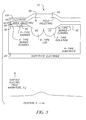
- the CCD 10 includes a p-type substrate 20 having a plurality of n-type buried channels 30 for collecting incident light in the form of electrons.
- a plurality of barriers 40 is disposed in the substrate 20 and defines a maximum energy level for charge collection in the burried channel 30, over which excess photogenerated electrical charges flow.
- a dielectric 50 is formed (deposited or grown) atop the buried channel 30 and extends over the barrier 40, lateral overflow drain 60 and channel stop 70. Both latter components are described in detail herein below.
- the dielectric 50 includes a thin, active area dielectric region 80 positioned substantially above the buried channel 30 and barrier 40, and includes a thick dielectric region 90 positioned substantially between the spaced-apart buried channels 30.
- a gate electrode 100 is disposed atop the entire dielectric 50.
- the active area dielectric 80 is preferably comprised of either oxide-nitride-oxide (ONO), oxide-nitride (ON), or oxide, and the thick dielectric 90 is preferably comprised of oxide, as this simplifies the manufacturing process.
- the n-type drain 60 is positioned substantially (either wholly or for the most part) in its entirety beneath a portion of the thick field dielectric 90 for collecting the excess photogenerated electrical charges flowing over the barrier 40.
- the p-type channel stop 70 is preferably positioned adjacent the lateral overflow drain 60 also substantially in its entirety beneath a portion of the thick field dielectric 90 for forming a boundary for the drain region 60. It is instructive to note that the p-type channel need not be positioned under the thick field dielectric as other positions are also viable.
- the lateral overflow drain 60 is insulated from the gate electrode 100 by a thick dielectric layer 90 (for example, 3000 to 4000 angstroms of oxide instead of 500 angstroms as in the prior art), a much lower electric field results at the silicon surface.
- a representative plot of the surface electric field strength versus position is also included in Fig. 3 for the CCD and its antiblooming structure 10 of the present invention and should be compared with the plot in Fig. 1 for the conventional lateral overflow drain structure.
- the lower electric field means that a greater amount of n-type impurities can be used in the LOD formation, which provides substantial improvements in the conductance when compared with the conventional design.
- the improved conductance can be used to significantly narrow the LOD width, and therefore permit the design of higher resolution (i.e., smaller pixels) imaging arrays without sacrificing charge capacity in the pixels.
- the higher breakdown voltages for the new structures could be used to improve device yield by permitting a larger operational range of applied voltages on the gate and LOD electrodes.
- Another important advantage of the lateral overflow drain structure of the present invention is the preferential use of arsenic impurities rather than phosphorus impurities as the n-type dopant.
- phosphorus had been favored due to its higher conductance and higher breakdown voltage relative to those of arsenic.
- the disadvantage of phosphorus is its long diffusion length that causes the LOD barrier potential to be pulled down, thereby reducing the charge capacity.
- Use of boron co-implanted with the phosphorus, and/or an adjustment in the LOD barrier implant dose, is generally required to counteract the pull-down effect of the phosphorus, adding complexity to the device processing.
- the potential in the channel stop region likewise, is subject to pull-down by the LOD formed with phosphorus impurities.
- An LOD under the field dielectric with arsenic impurities diffuses much more slowly than one formed with phosphorus impurities, and therefore exerts much less of an influence on neighboring potentials in the pixel.
- the use of co-implanted boron impurities to compensate for the presence of the phosphorus impurities is therefore unnecessary, which further improves drain conductivity.
- the need for adjustment in the barrier implant is also reduced.
- the use of arsenic for the LOD formation is clearly preferred for pixel scaling efforts intended to improve image resolution.
- an n-type substrate could be used by using the opposite conductivity types for the various other implants. It is also to be understood that, although the drawings show only one CCD and its corresponding lateral overflow drain, there are a plurality of such CCDs and their corresponding lateral overflow drain, anti-blooming structures.
Landscapes
- Solid State Image Pick-Up Elements (AREA)
- Transforming Light Signals Into Electric Signals (AREA)
Applications Claiming Priority (2)
| Application Number | Priority Date | Filing Date | Title |
|---|---|---|---|
| US945034 | 1978-09-22 | ||
| US09/945,034 US6624453B2 (en) | 2001-08-31 | 2001-08-31 | Lateral overflow drain, anti-blooming structure for CCD devices having improved breakdown voltage |
Publications (3)
| Publication Number | Publication Date |
|---|---|
| EP1289020A2 EP1289020A2 (en) | 2003-03-05 |
| EP1289020A3 EP1289020A3 (en) | 2004-04-21 |
| EP1289020B1 true EP1289020B1 (en) | 2009-08-19 |
Family
ID=25482511
Family Applications (1)
| Application Number | Title | Priority Date | Filing Date |
|---|---|---|---|
| EP02078413A Expired - Lifetime EP1289020B1 (en) | 2001-08-31 | 2002-08-19 | A lateral overflow drain, antiblooming structure for CCD devices having improved breakdown voltage |
Country Status (4)
| Country | Link |
|---|---|
| US (1) | US6624453B2 (enExample) |
| EP (1) | EP1289020B1 (enExample) |
| JP (1) | JP2003086782A (enExample) |
| DE (1) | DE60233371D1 (enExample) |
Families Citing this family (13)
| Publication number | Priority date | Publication date | Assignee | Title |
|---|---|---|---|---|
| US7899339B2 (en) * | 2002-07-30 | 2011-03-01 | Amplification Technologies Inc. | High-sensitivity, high-resolution detector devices and arrays |
| GB2428516A (en) * | 2004-03-18 | 2007-01-31 | E2V Tech Uk Ltd | Radiation tolerant CCD structure |
| JP4967237B2 (ja) * | 2005-01-28 | 2012-07-04 | パナソニック株式会社 | 固体撮像装置 |
| US7893981B2 (en) * | 2007-02-28 | 2011-02-22 | Eastman Kodak Company | Image sensor with variable resolution and sensitivity |
| JP2009177018A (ja) * | 2008-01-25 | 2009-08-06 | Sanyo Electric Co Ltd | 固体撮像素子及びその製造方法 |
| EP2359402B1 (en) * | 2008-12-10 | 2012-10-24 | Truesense Imaging, Inc. | Method of fabricating image sensors with lateral overflow drains |
| US8772891B2 (en) | 2008-12-10 | 2014-07-08 | Truesense Imaging, Inc. | Lateral overflow drain and channel stop regions in image sensors |
| JP5243983B2 (ja) * | 2009-01-30 | 2013-07-24 | 浜松ホトニクス株式会社 | 電子増倍機能内蔵型の固体撮像素子 |
| US9070611B2 (en) | 2011-07-29 | 2015-06-30 | Semiconductor Components Industries, Llc | Image sensor with controllable vertically integrated photodetectors |
| US8829637B2 (en) | 2011-07-29 | 2014-09-09 | Semiconductor Components Industries, Llc | Image sensor with controllable vertically integrated photodetectors using a buried layer |
| US8946612B2 (en) * | 2011-07-29 | 2015-02-03 | Semiconductor Components Industries, Llc | Image sensor with controllable vertically integrated photodetectors |
| US8847285B2 (en) | 2011-09-26 | 2014-09-30 | Semiconductor Components Industries, Llc | Depleted charge-multiplying CCD image sensor |
| US10341590B2 (en) * | 2016-08-12 | 2019-07-02 | Semiconductor Components Industries, Llc | Methods and apparatus for a CCD image sensor |
Family Cites Families (4)
| Publication number | Priority date | Publication date | Assignee | Title |
|---|---|---|---|---|
| US4774557A (en) * | 1986-05-15 | 1988-09-27 | General Electric Company | Back-illuminated semiconductor imager with charge transfer devices in front surface well structure |
| US4984047A (en) * | 1988-03-21 | 1991-01-08 | Eastman Kodak Company | Solid-state image sensor |
| JP3592772B2 (ja) * | 1994-12-19 | 2004-11-24 | 株式会社東芝 | 固体撮像装置 |
| US6608337B2 (en) * | 2001-04-12 | 2003-08-19 | Ise Tex, Inc | Image sensor with an enhanced near infra-red spectral response and method of making |
-
2001
- 2001-08-31 US US09/945,034 patent/US6624453B2/en not_active Expired - Lifetime
-
2002
- 2002-08-19 DE DE60233371T patent/DE60233371D1/de not_active Expired - Lifetime
- 2002-08-19 EP EP02078413A patent/EP1289020B1/en not_active Expired - Lifetime
- 2002-08-21 JP JP2002240045A patent/JP2003086782A/ja active Pending
Also Published As
| Publication number | Publication date |
|---|---|
| US20030042510A1 (en) | 2003-03-06 |
| EP1289020A2 (en) | 2003-03-05 |
| DE60233371D1 (de) | 2009-10-01 |
| EP1289020A3 (en) | 2004-04-21 |
| US6624453B2 (en) | 2003-09-23 |
| JP2003086782A (ja) | 2003-03-20 |
Similar Documents
| Publication | Publication Date | Title |
|---|---|---|
| JP3570733B2 (ja) | 仮想位相フレーム・インタライン転送ccd画像センサ | |
| US5130774A (en) | Antiblooming structure for solid-state image sensor | |
| KR980012585A (ko) | 수직형 전달게이트를 가지는 전하결합형 고체촬상소자 및 그 제조방법 | |
| US7619675B2 (en) | Solid-state image taking apparatus with photoelectric converting and vertical charge transferring sections and method for fabricating the same | |
| EP1289020B1 (en) | A lateral overflow drain, antiblooming structure for CCD devices having improved breakdown voltage | |
| US11695029B2 (en) | Pixel formation method | |
| KR0130959B1 (ko) | 고체촬상장치 및 그 제조방법 | |
| KR100280014B1 (ko) | 증폭형 광전변환소자 및 그의 제조방법 및 증폭형 고체촬상장치 | |
| EP0240238B1 (en) | Solid state imager device | |
| US5235196A (en) | Transfer region design for charge-coupled device image sensor | |
| WO1990016083A1 (en) | Charge-coupled imager with dual gate anti-blooming structure | |
| US7804113B2 (en) | Anti-blooming structures for back-illuminated imagers | |
| KR100741559B1 (ko) | 고체 촬상 소자 및 그 제조 방법 | |
| JP4359739B2 (ja) | 光電変換素子および固体撮像素子 | |
| US5714776A (en) | Compact isolation and antiblooming structure for full-frame CCD image sensors operated in the accumlation mode | |
| US6794219B1 (en) | Method for creating a lateral overflow drain, anti-blooming structure in a charge coupled device | |
| JPH07211883A (ja) | 固体撮像装置及びその製造方法 | |
| JPH0846168A (ja) | 固体撮像装置 | |
| JP3160382B2 (ja) | 固体撮像装置 | |
| JP4577737B2 (ja) | 固体撮像装置 | |
| EP0069649B1 (en) | Self-aligned antiblooming structure for charge-coupled devices and method of fabrication thereof | |
| US5804844A (en) | Solid-state imager with container LOD implant | |
| JP5030323B2 (ja) | 固体撮像素子 | |
| JP3238160B2 (ja) | 積層形固体撮像装置 | |
| JP3712516B2 (ja) | 固体撮像装置及びその製造方法 |
Legal Events
| Date | Code | Title | Description |
|---|---|---|---|
| PUAI | Public reference made under article 153(3) epc to a published international application that has entered the european phase |
Free format text: ORIGINAL CODE: 0009012 |
|
| AK | Designated contracting states |
Kind code of ref document: A2 Designated state(s): AT BE BG CH CY CZ DE DK EE ES FI FR GB GR IE IT LI LU MC NL PT SE SK TR Designated state(s): AT BE BG CH CY CZ DE DK EE ES FI FR GB GR IE IT LI LU MC NL PT SE SK TR |
|
| AX | Request for extension of the european patent |
Extension state: AL LT LV MK RO SI |
|
| PUAL | Search report despatched |
Free format text: ORIGINAL CODE: 0009013 |
|
| AK | Designated contracting states |
Kind code of ref document: A3 Designated state(s): AT BE BG CH CY CZ DE DK EE ES FI FR GB GR IE IT LI LU MC NL PT SE SK TR |
|
| AX | Request for extension of the european patent |
Extension state: AL LT LV MK RO SI |
|
| 17P | Request for examination filed |
Effective date: 20040913 |
|
| AKX | Designation fees paid |
Designated state(s): DE FR GB |
|
| 17Q | First examination report despatched |
Effective date: 20050117 |
|
| R17C | First examination report despatched (corrected) |
Effective date: 20050117 |
|
| GRAP | Despatch of communication of intention to grant a patent |
Free format text: ORIGINAL CODE: EPIDOSNIGR1 |
|
| RTI1 | Title (correction) |
Free format text: A LATERAL OVERFLOW DRAIN, ANTIBLOOMING STRUCTURE FOR CCD DEVICES HAVING IMPROVED BREAKDOWN VOLTAGE |
|
| GRAS | Grant fee paid |
Free format text: ORIGINAL CODE: EPIDOSNIGR3 |
|
| GRAA | (expected) grant |
Free format text: ORIGINAL CODE: 0009210 |
|
| AK | Designated contracting states |
Kind code of ref document: B1 Designated state(s): DE FR GB |
|
| REG | Reference to a national code |
Ref country code: GB Ref legal event code: FG4D |
|
| REF | Corresponds to: |
Ref document number: 60233371 Country of ref document: DE Date of ref document: 20091001 Kind code of ref document: P |
|
| PLBE | No opposition filed within time limit |
Free format text: ORIGINAL CODE: 0009261 |
|
| STAA | Information on the status of an ep patent application or granted ep patent |
Free format text: STATUS: NO OPPOSITION FILED WITHIN TIME LIMIT |
|
| 26N | No opposition filed |
Effective date: 20100520 |
|
| REG | Reference to a national code |
Ref country code: GB Ref legal event code: 732E Free format text: REGISTERED BETWEEN 20110704 AND 20110706 |
|
| REG | Reference to a national code |
Ref country code: FR Ref legal event code: TP Owner name: OMNI VISION TECHNOLOGIES, INC., US Effective date: 20110829 |
|
| REG | Reference to a national code |
Ref country code: FR Ref legal event code: PLFP Year of fee payment: 15 |
|
| REG | Reference to a national code |
Ref country code: FR Ref legal event code: PLFP Year of fee payment: 16 |
|
| REG | Reference to a national code |
Ref country code: FR Ref legal event code: PLFP Year of fee payment: 17 |
|
| PGFP | Annual fee paid to national office [announced via postgrant information from national office to epo] |
Ref country code: FR Payment date: 20210728 Year of fee payment: 20 |
|
| PGFP | Annual fee paid to national office [announced via postgrant information from national office to epo] |
Ref country code: DE Payment date: 20210713 Year of fee payment: 20 Ref country code: GB Payment date: 20210728 Year of fee payment: 20 |
|
| REG | Reference to a national code |
Ref country code: DE Ref legal event code: R071 Ref document number: 60233371 Country of ref document: DE |
|
| REG | Reference to a national code |
Ref country code: GB Ref legal event code: PE20 Expiry date: 20220818 |
|
| PG25 | Lapsed in a contracting state [announced via postgrant information from national office to epo] |
Ref country code: GB Free format text: LAPSE BECAUSE OF EXPIRATION OF PROTECTION Effective date: 20220818 |