EP1271808B1 - Emetteur optique et système de transmission optique - Google Patents
Emetteur optique et système de transmission optique Download PDFInfo
- Publication number
- EP1271808B1 EP1271808B1 EP02291611A EP02291611A EP1271808B1 EP 1271808 B1 EP1271808 B1 EP 1271808B1 EP 02291611 A EP02291611 A EP 02291611A EP 02291611 A EP02291611 A EP 02291611A EP 1271808 B1 EP1271808 B1 EP 1271808B1
- Authority
- EP
- European Patent Office
- Prior art keywords
- optical
- signal
- output
- input
- transmission system
- Prior art date
- Legal status (The legal status is an assumption and is not a legal conclusion. Google has not performed a legal analysis and makes no representation as to the accuracy of the status listed.)
- Expired - Lifetime
Links
Images


Classifications
-
- H—ELECTRICITY
- H04—ELECTRIC COMMUNICATION TECHNIQUE
- H04B—TRANSMISSION
- H04B10/00—Transmission systems employing electromagnetic waves other than radio-waves, e.g. infrared, visible or ultraviolet light, or employing corpuscular radiation, e.g. quantum communication
- H04B10/50—Transmitters
- H04B10/516—Details of coding or modulation
- H04B10/548—Phase or frequency modulation
- H04B10/556—Digital modulation, e.g. differential phase shift keying [DPSK] or frequency shift keying [FSK]
- H04B10/5561—Digital phase modulation
-
- H—ELECTRICITY
- H04—ELECTRIC COMMUNICATION TECHNIQUE
- H04B—TRANSMISSION
- H04B10/00—Transmission systems employing electromagnetic waves other than radio-waves, e.g. infrared, visible or ultraviolet light, or employing corpuscular radiation, e.g. quantum communication
- H04B10/50—Transmitters
- H04B10/501—Structural aspects
- H04B10/503—Laser transmitters
- H04B10/505—Laser transmitters using external modulation
- H04B10/5051—Laser transmitters using external modulation using a series, i.e. cascade, combination of modulators
-
- H—ELECTRICITY
- H04—ELECTRIC COMMUNICATION TECHNIQUE
- H04B—TRANSMISSION
- H04B10/00—Transmission systems employing electromagnetic waves other than radio-waves, e.g. infrared, visible or ultraviolet light, or employing corpuscular radiation, e.g. quantum communication
- H04B10/50—Transmitters
- H04B10/501—Structural aspects
- H04B10/503—Laser transmitters
- H04B10/505—Laser transmitters using external modulation
- H04B10/5055—Laser transmitters using external modulation using a pre-coder
-
- H—ELECTRICITY
- H04—ELECTRIC COMMUNICATION TECHNIQUE
- H04B—TRANSMISSION
- H04B10/00—Transmission systems employing electromagnetic waves other than radio-waves, e.g. infrared, visible or ultraviolet light, or employing corpuscular radiation, e.g. quantum communication
- H04B10/50—Transmitters
- H04B10/516—Details of coding or modulation
- H04B10/5162—Return-to-zero modulation schemes
-
- H—ELECTRICITY
- H04—ELECTRIC COMMUNICATION TECHNIQUE
- H04B—TRANSMISSION
- H04B10/00—Transmission systems employing electromagnetic waves other than radio-waves, e.g. infrared, visible or ultraviolet light, or employing corpuscular radiation, e.g. quantum communication
- H04B10/60—Receivers
- H04B10/66—Non-coherent receivers, e.g. using direct detection
- H04B10/67—Optical arrangements in the receiver
- H04B10/676—Optical arrangements in the receiver for all-optical demodulation of the input optical signal
- H04B10/677—Optical arrangements in the receiver for all-optical demodulation of the input optical signal for differentially modulated signal, e.g. DPSK signals
-
- H—ELECTRICITY
- H04—ELECTRIC COMMUNICATION TECHNIQUE
- H04J—MULTIPLEX COMMUNICATION
- H04J14/00—Optical multiplex systems
- H04J14/02—Wavelength-division multiplex systems
- H04J14/0227—Operation, administration, maintenance or provisioning [OAMP] of WDM networks, e.g. media access, routing or wavelength allocation
- H04J14/0241—Wavelength allocation for communications one-to-one, e.g. unicasting wavelengths
- H04J14/0242—Wavelength allocation for communications one-to-one, e.g. unicasting wavelengths in WDM-PON
- H04J14/0245—Wavelength allocation for communications one-to-one, e.g. unicasting wavelengths in WDM-PON for downstream transmission, e.g. optical line terminal [OLT] to ONU
- H04J14/0246—Wavelength allocation for communications one-to-one, e.g. unicasting wavelengths in WDM-PON for downstream transmission, e.g. optical line terminal [OLT] to ONU using one wavelength per ONU
-
- H—ELECTRICITY
- H04—ELECTRIC COMMUNICATION TECHNIQUE
- H04B—TRANSMISSION
- H04B2210/00—Indexing scheme relating to optical transmission systems
- H04B2210/517—Optical NRZ to RZ conversion, or vice versa
-
- H—ELECTRICITY
- H04—ELECTRIC COMMUNICATION TECHNIQUE
- H04J—MULTIPLEX COMMUNICATION
- H04J14/00—Optical multiplex systems
- H04J14/02—Wavelength-division multiplex systems
- H04J14/0227—Operation, administration, maintenance or provisioning [OAMP] of WDM networks, e.g. media access, routing or wavelength allocation
-
- H—ELECTRICITY
- H04—ELECTRIC COMMUNICATION TECHNIQUE
- H04J—MULTIPLEX COMMUNICATION
- H04J14/00—Optical multiplex systems
- H04J14/02—Wavelength-division multiplex systems
- H04J14/0278—WDM optical network architectures
- H04J14/0279—WDM point-to-point architectures
Definitions
- the present invention relates to an optical transmitter and an optical transmission system that can minimize the deterioration in the transmission quality due to the chromatic dispersion of an optical transmission medium such as an optical fiber, or due to the interaction between the chromatic dispersion and nonlinear optical effects.
- An RZ (return-to-zero) optical intensity modulation format used along with phase modulation has been proposed having the object of minimizing the deterioration in the transmission quality due to the chromatic dispersion of an optical transmission medium such as an optical fiber, or due to the interaction between the chromatic dispersion and nonlinear optical effects.
- DCS-RZ duobinary carrier-suppressed return-to-zero
- European patent application EP 0 825 733 A2 discloses a method of generating duobinary signals and an optical transmitter using the same method.
- FIG- 41 is a diagram for explaining the conventional structure of an optical transmitter that uses a DCS-RZ format.
- a direct current bias is applied to the first push-pull type Mach-Zehnder (MZ) optical intensity modulator 91 so as to realize transmission-null when unmodulated, and the first push-pull type Mach-Zehnder optical intensity modulator 91 is complementarily driven by an electrical sine wave signal having one-half the frequency of the line rate generated by a half frequency divider 92.
- MZ Mach-Zehnder
- the intensity and phase of the CW light output from the single longitudinal mode LD 90 which is the light source of the carrier frequency f 0 , are simultaneously modulated by the MZ optical intensity modulator 91 using the frequency multiplier function and the phase modulation function of an MZ optical intensity modulator, and a dual mode beat signal having a repetition frequency of B is generated.
- B is the line rate.
- the dual mode beat signal is modulated with data using an optical duobinary format.
- the input NRZ (non-return-to-zero) signal is converted to a pre-coded NRZ code by the precoder circuit 97 that is formed by the logic inversion circuit 94, the exclusive OR circuit 95, and the 1 bit delay circuit 96, and the pre-coded NRZ code is differentially output.
- the differential pre-coded NRZ code is amplified by the baseband amplifier 98, and then converted to a complementary ternary electrical duobinary code by the low pass filter (LPF 99) having 3dB bandwidth of B/4.
- a direct current bias is applied to the second MZ optical modulator 93 so as to realize transmission-null when unmodulated, and the second MZ optical modulator 93 modulates with a complementary ternary electrical duobinary code to generate a DCS-RZ optically modulated code.
- FIGS. 42A through 42F and FIG. 43A and 43B show an example of the operation of the conventional technology.
- FIG. 42A shows the binary NRZ signal input generated by the binary NRZ signal generating unit 103.
- FIG. 42B shows the NRZ data signal output from the logic inversion circuit 94 in the case that a binary NRZ signal is input.
- FIG. 42C shows the positive-phase signal output from the pre-coding circuit 97 in the case that the output NRZ data signal is input, and the logic thereof is inverted each time a space bit is input as the input NRZ signal.
- FIG. 42D shows the waveform output from the LPF 99 in the case that the pre-coded signal is input.
- the logical operation of the LPF 99 is identical to that of a circuit block comprising the 1 bit delay circuit 101 and the analog AND circuit 102. Due to the band limiting function of the LPF 99, the complementary ternary electrical duobinary signal shown by the bold solid line is generated.
- FIG. 42E shows the electrical field waveform of the dual mode beat optical signal modulated by the first MZ optical intensity modulator 91 when the CW optical signal from the LD 90, which is the light source, is input.
- the electrical field waveform forms an optical pulse train where the repetition frequency is equal to the line rate, and whose optical phase is alternate ⁇ phase flip for each bit.
- This dual mode beat optical signal is modulated with the ternary electrical duobinary signal shown in FIG. 42D , and thereby the DCS-RZ code shown in FIG. 42F is generated. The phase is inverted for each mark bit, and thus an RZ intensity modulated optical data signal is obtained.
- FIG. 43A shows the optical spectrum of the dual mode beat signal output from the first MZ optical intensity modulator 91.
- the optical carrier signal component f 0 is suppressed, and at the optical frequency fb ⁇ (B/2) (where B is the line rate), two longitudinal modes having a frequency spacing of B are generated.
- the two longitudinal modes are modulated with each of the optical duobinary codes by the second MZ optical modulator 93.
- the optical modulated spectrum of the generated DCS-RZ optical signal is comprised of two optical duobinary signal modulated spectrum arranged at optical frequencies f 0 ⁇ B, the carrier component is completely suppressed, and the optical modulation band is narrowed to 2B.
- the tolerance with respect to chromatic dispersion is double that of the conventional RZ.
- the above format suppresses the impairment of the optical duobinary code due to optical nonlinear effects, and thus RZ encoding can be realized while suppressing the broadening of the optical modulation band.
- this is suitable as a modulation format in a dense wavelength division multiplexing transmission system.
- T. Miyano et al. propose an RZ-intensity-modulated phase-encoded signal in citation 2, T. Miyano, M. Fukutoku, and K.
- optical modulators are necessary for each intensity modulation, phase encoding, and pulse modulation, and these optical modulators are connected in a multi-stage cascade.
- the insertion loss in the modulating unit increases, and the optical output power of the modulating unit decreases.
- the optical signal shot noise increases and the SN ratio of the output of the optical transmitting unit degrades.
- the optical duobinary encoding unit which carries out the intensity data modulation and phase modulation in data encoding process requires a baseband analog processing circuit (LPF 99 shown in FIG. 41 ) that generates a ternary opto-electrical signal converted signal depending on the line rate.
- LPF 99 baseband analog processing circuit
- the conventional PSK signal that has been modulated using an RZ format can suppress the cross-phase modulation in a wavelength division multiplexing system.
- the optical modulation band spreads four times the line rate, and thus the cross-talk penalty increases.
- it is necessary to increase the operating speed of the baseband signal input into the modulator.
- the invention measures the increasing speed of the analog signal processing by performing a function in the optical carrier frequency domain, which has been carried out by a conventional baseband analog processing circuit.
- the invention facilitates realization of an amplifier circuit such as a driver circuit by encoding all the electric signals with a simple binary NRZ format.
- the invention concerns an optical transmitter and an optical transmission system as defined in the claims.
- the optical transmitter of the present invention comprises: a light source; a pre-coding device that receives an NRZ signal; an optical phase modulating device that carries out optical phase modulation and that is driven by either a pre-coded NRZ signal or a differential pre-coded NRZ signal generated by the pre-cording device; and an output terminal, wherein an RZ optical signal in which a plurality of duobinary optical signal components are included in the optical RZ signal spectrum with carrier suppression is output from the output terminal.
- the optical transmitter of the present invention comprises: a light source which is a single mode longitudinal light source; a pre-coding device that generates a differential pre-coded NRZ signal whose logic inverts each time a mark bit is input as an NRZ signal; an optical phase modulating device that modulates the optical phase of a single longitudinal mode optical signal from the light source using the differential pre-coded NRZ signal generated by the pre-coding device; and an optical filter device that converts an optical-phase modulated signal generated by the optical phase modulating device to an RZ optical intensity modulated signal.
- the optical transmitter of the present invention further comprises: a dual mode beat pulse light source that generates two longitudinal mode signals which synchronizes with a data signal and which have the mode spacing between the two longitudinal modes that is an integral multiple of the data line rate, and which is mode-locked with each other; a pre-coding device that carries out code conversion such that an intensity modulated signal output from the optical transmitter has a logic identical to the input NRZ signal; and an optical phase modulating device in which an optical pulse train generated by the dual mode beat pulse light source has undergone optical phase modulation by a pre-coded NRZ signal generated by the pre-coding device.
- the optical transmission system of the present invention comprises: an optical transmitter that comprises: a light source; a pre-coding device that receives an NRZ signal; an optical phase modulating device that carries out optical phase modulation and that is driven by either a pre-coded NRZ signal or a differential pre-coded NRZ signal generated by the pre-coding device; and an output terminal, and that outputs an RZ optical signal having the suppressed carrier component from the output terminal as an optical transmission signal; an optical phase-modulation/amplitude modulation converting device that is provided on one of either the optical transmitter or an optical receiver; wherein the optical receiver demodulates and detects the transmitted RZ optical signal as an optical intensity modulated signal, and converts the optical intensity modulated signal to an electrical signal.
- the optical transmission system of the present invention comprises: an optical transmitter that comprises: a pre-coding device that generates a differential pre-coded NRZ signal whose logic inverts each time a mark bit is input as the NRZ signal; an optical phase modulating device that performs optical phase modulation on a signal from either a single longitudinal mode light source or a dual mode beat pulse light source using the differential pre-coded NRZ signal generated by the pre-coding device; and an optical filter device that converts an optical phase modulated signal generated by the optical phase modulating device into an RZ optical intensity modulated signal; an optical transmission medium that transmits the RZ optical intensity modulated signal output by the optical transmitter; and an optical receiver that receives the RZ optical intensity modulated signal output by the optical transmitter via the optical transmission medium, and directly detects the RZ optical intensity modulated signal to convert the RZ optical intensity modulated signal into a baseband electrical signal.
- an optical transmitter that comprises: a pre-coding device that generates a differential pre-coded NRZ signal whose logic inverts
- the optical transmission system of the present invention comprises: an optical transmitter that is provided with: a pre-coding device that carries out code conversion of the input NRZ signal such that the optical intensity modulated signal output from the optical transmitter has a logic identical to the input NRZ signal; and an optical phase modulating device that performs optical phase modulation on a signal either from a single longitudinal-mode light source or a dual mode beat pulse light source using the differential pre-coded NRZ signal generated by the pre-coding device; an optical transmission medium that transmits a phase modulated data signal with sinusoidal RZ optical intensity modulation that has been output by the optical transmitter; and an optical receiver that receives the RZ optical modulated signal output by the optical transmitter via the optical transmission medium, and after passing through an optical filter device that converts the RZ optical modulated phase-encoded signal to an optical amplitude-encoded signal, directly detects the optical intensity modulated signal to convert to a baseband electrical signal.
- the baseband input data signal is pre-coded in advance by the pre-coding device, phase modulation is carried out by the phase modulating device using the pre-coded signal, and the resultant phase encoded optical signal is converted into an RZ intensity modulated signal that has undergone the phase modulation by the optical filter device.
- the phase modulating device for example, generates an encoded DPSK phase modulation signal using differential phase shift keying (DPSK), and converts the phase modulated signal into an RZ intensity signal by the optical filter device disposed downstream of the DPSK optical modulation signal device.
- DPSK differential phase shift keying
- an optical periodic filter is used as the optical filter device described above, conversion of modulation format of the wavelength division multiplexed signals can be simultaneously conducted due to the broadband characteristic or the optical filter, and thus an optical filter device for each channel becomes unnecessary. Thereby, the number of parts can be drastically reduced in the high capacity wavelength division multiplexing system having a large number of channels, and thereby the cost of the optical transmitter can be reduced. In addition, by using a passive optical filter that does not require high-speed signals, precise control of the signal phase between modulators becomes unnecessary.
- the phase modulating device that carries out differential phase shift keying on the single longitudinal mode optical signal using a pre-coded NRZ signal
- the analog processing function conventionally carried out in the baseband can be realized in an optical carrier frequency band using a passive optical filter, and thereby, an ideal wideband analog processing can be realized, and improvement of the reflective characteristics in the filter processing and the broadband transmission characteristics becomes possible for generation of the ultra-high-speed signal.
- an optical filter that carries out phase modulation/RZ intensity modulation conversion is disposed on the receiver side of the optical transmission system, phase encoded signal is used as a transmission code, and an RZ pulse whose intensity has been phase encoded is used.
- the phase modulating device can be structured by n phase modulators connected in series.
- All of these multiplexed signals are bandwidth-reduced RZ signals, and can form a high-density wavelength division multiplexing system using a simple structure in comparison to conventional technology.
- the optical transmitter in order to realize a high speed optical transmitter and optical transmission system using the RZ optical intensity modulation format used with phase modulation, the optical transmitter is provided with a pre-coding device that generates a differential pre-coded NRZ signal whose logic inverts each time a mark bit is input as an NRZ signal; an optical phase modulation device that carries out optical phase modulation on a single longitudinal mode optical signal generated by a light source using the differential pre-coded NRZ signal generated by the pre-coding device; and an optical filter device that converts the phase modulated optical signal generated by the optical phase modulating device to an RZ optical intensity modulated signal.
- the loss of the optical modulator is decreased and enhancing the high-speed operation of the optical modulator becomes easy.
- the speed of the analog signal conversion processing can be increased, and furthermore, by making all electrical signals binary NRZ format, the amplifier circuits such as drive circuits can be easily realized.
- phase modulated wavelength division multiplexed signals becomes possible by the parallel processing of the optical filter.
- phase modulating a dual mode beat pulse signal an RZ phase modulated code or an intensity modulated code having a constant duty cycle can be used as the transmission code. Therefore, narrowing of the optical modulation bandwidth becomes possible, and the efficiency for frequency utilization of the wavelength division multiplexing system can be improved. At the same time, the tolerance of transmission quality degradation due to nonlinear effects can be improved.
- the chromatic dispersion tolerance can be improved.
- an increase in the system line rate can be realized without enhancing the operation speed of the pre-coding circuit, the modulator, and the driver for the modulator.
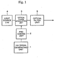
- FIG. 1 is a block diagram showing an embodiment of the optical transmitter according to the present invention.
- the binary NRZ electrical signal output from the NRZ signal generating unit 1 is input into the pre-coding unit 2.
- the pre-coding unit 2 carries out signal processing so that the optical signal output from the optical transmitter matches the input NRZ signal.
- the differential pre-coded NRZ signal generated by the pre-coding unit 2 is amplified as necessary, and input into the optical phase modulating unit 3.
- the single longitudinal mode CW optical signal emitted by the light source 4 (LD: a laser diode) is appropriately phase modulated by the optical phase modulating unit 3, and subsequently input into the optical filter unit 5 that converts the optical phase modulated signal into an RZ intensity modulated signal.
- the output of the optical filter unit 5 is optically amplified as necessary, and is output as the output signal of the optical transmitter according to the present invention at a predetermined optical power.
- FIG. 2 shows the detailed structure of each of the blocks of the optical transmitter shown in FIG. 1 .
- blocks having the same reference numerals as the blocks shown in FIG. 1 are the same as those in FIG. 1 .
- the NRZ electrical signal output from the NRZ signal generating unit 1 is input into the pre-coding unit 2.
- the pre-coding unit 2 is formed by an exclusive OR circuit (EXOR 21), a 1-bit delay circuit 22, and a differential output circuit 23.
- the pre-coding unit 2 differs from the conventional pre-coding unit 97 ( FIG. 41 ) in that there is not a logic inversion circuit 94 for inverting the logic of the input data signal.
- the pre-coding unit 2 shown in FIG. 2 carries out differential encoding, thereby a differentially pre-coded encoded NRZ signal whose logic is inverted each time a mark bit is input as the input NRZ signal is differentially output.
- the differentially encoded NRZ signal is input into the optical phase modulating unit 3.
- the optical phase modulating unit 3 amplifies the signal as necessary by using the baseband amplifier 31, and supplies it to the MZ optical intensity modulator 32.
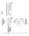
- FIG. 3 is a diagram for explaining the operation of the MZ optical intensity modulator 32 shown in FIG. 2 .
- the differentially encoded NRZ signal generated by the pre-coding unit 2 is amplified to equal amplitudes, preferably amplified up to half-wave voltage of the MZ optical intensity modulator 32.
- the direct current bias is applied to the MZ optical intensity modulator 32 so as to realize transmission-null when unmodulated.
- the MZ optical intensity modulator 32 generates the DPSK optical signal that is encoded using a DPSK (differential phase shift keying) format.
- the DPSK optical signal is input into the Mach-Zehnder interferometer (MZI) type optical filter that forms the optical filter unit 5 and whose rejection band center frequency matches the optical carrier frequency of the DPSK optical signal.
- the MZI optical filter is formed by 3 dB directional couplers (52 and 53) disposed at the input port 51 and the cross output port 56, and an optical delay element 54 having a delay of ⁇ (s).
- an optical signal input into the through port 5 is Ein (i.e., input optical signal electric field)
- ⁇ is the optical frequency
- ⁇ is the amount of delay of the optical delay element 54
- ⁇ is the relative phase between the two optical signals propagated through the waveguide in the Mach-Zehnder optical filter.
- FIGS. 4A through 4F are diagrams for explaining in detail the operation of the embodiment of the present invention.
- FIG. 4A shows the input NRZ baseband electrical signal (binary), and FIG. 4B shows the input pre-coded NRZ baseband electrical signal output from the pre-coding unit 2 in the case that the signal shown in FIG. 4A is input thereto.
- FIG. 4C shows the generated DPSK optical modulated signal that has been modulated by the MZ optical intensity modulator 32 with the pre-coded NRZ signal.
- FIG. 4D shows the DPSK optical signal at point C ( FIG. 2 ) in the MZI optical filter that has been delayed by ⁇ by the optical delay element 54.
- FIG. 4E shows the DPSK optical signal (the output signal from the Mach-Zehnder interferometer type optical filter) output from the MZI optical filter.
- the dashed line is the logical electrical field envelope
- the solid line is the DPSK optical signal for the case that optical phase modulation has been carried out with a bandwidth limit applied to the pre-coded NRZ electrical signal.
- FIG. 4F shows the directly detected waveform.
- FIG. 4E shows the RZ optical signal output from the through port 56 of the 3 dB directional coupler 53 of the MZI optical filter 51 according to the above Equation 1.
- the dashed line is the logical electrical field envelope
- the solid line is the electrical field envelope in the case that optical phase modulation has been carried out with a bandwidth limit applied to the pre-coded NRZ electrical signal.
- the MZI optical filter outputs a signal in accordance with a phase change rule that is identical to that of the DCS-RZ signal, whose phase is inverted with each mark bit.
- the optically modulated signal of the rejection band is separated by the 3 dB directional coupler 53 and output from the cross port 56.
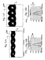
- FIGS. 5A through 5C and FIGS. 6A through 6C show the optically modulated spectra at the input port and output port of the MZI optical filter in FIG. 2 .
- FIGS. 5A and 6A show the DPSK optically modulated spectra at the point A shown in FIG. 2 .
- the ordinate is the scale for the spectral intensity, and the abscissa is the scale for the optical frequency.
- FIGS. 5B and 6B show the frequency response characteristics of the MZI optical filter 51 shown in FIG. 2 .
- the ordinate is the scale for the transmittance (dB), and the abscissa is the scale for the optical frequency.
- FIGS. 5A through 5C show a sine wave frequency response of period B (where B is the line rate).
- FIGS. 6A through 6C show a sine wave frequency response of period 2B.
- FIGS. 5C and 6C show the converted RZ signal optical modulated spectra. The ordinate is the scale for the spectral intensity and the abscissa is the scale for the optical frequency.
- the carrier frequency component is entirely suppressed, and the modulation spectrum has the modulation bandwidth of 2B.
- the RZ optical signal output from the optical filter unit 5 has the same coding rule as that used in a DCS-RZ format, as can be understood from the optical phase change rule of the waveform response shown in FIGS. 4A through 4F and the optically modulated spectra shown in FIGS. 5A through 5C and FIGS. 6A through 6C .
- FIG. 7 is a diagram for explaining the operation in the case that the optical phase modulating unit 3 shown in FIG. 2 is realized by another structure.
- the difference between the example shown in FIG. 7 and the embodiment shown in FIG. 2 is that the optical pulse is chirped so that the optical phase thereof changes over time and that optical intensity thereof does not change.
- FIG. 7 the optical phase responses for each of the points (a, b, c, d) is output corresponding to each of the points (a, b, c, d) in the baseband pre-coded NRZ electrical signal input. That is, FIG. 7 shows response characteristics in which the optical phase changes linearly. These types of characteristics can be easily realized by an optical phase modulator which modulates the refractive index of the straight optical waveguide formed, for example, on LiNbO 3 by means of an electro-optical effect.
- FIG. 8 is a diagram for showing another embodiment of the optical filter unit 5 shown in FIG. 2 .
- the embodiment shown in FIG. 8 differs from the embodiment shown in FIG. 2 in that instead of the 3 dB directional couplers 52 and 53, the Y-branching waveguides 58 and 59 are used in the optical branching unit of the Mach-Zehnder interferometer type filter that forms the optical filter unit 5.
- the DPSK optical signal input from the optical input port 57 is branched into two paths by the Y-branching waveguide 58 such that the power is 50% in each.
- One optical signal passes through the optical delay element 54 having a delay amount ⁇ , is multiplexed with another optical signal by the Y-branching waveguide 59, and the multiplexed optical signal is output from the output port 60.
- FIG. 9 is a diagram showing an embodiment of the optical transmission system according to the present invention. Because the optical transmitter 61 used is identical to the embodiment described above, the explanation will be omitted in order to avoid repetition.
- the binary NRZ input electrical signal is converted to an RZ signal by the optical transmitter 61, is optically amplified by the optical amplifier 62 as necessary to a predetermined signal power, and is subsequently supplied to the optical transmission medium 69.
- the optical transmission medium 69 can be formed from only an optical fiber transmission line 63.
- the optical transmission medium 69 can be formed by optical transmission lines 63 and optical amplifier repeater devices 64 that directly amplify and repeat the optical signals from the optical transmission lines 63.
- the output signal of the optical transmission medium 69 is input into the optical receiver 65.
- the input optical signal is pre-amplified by the optical amplifier 62, and then as necessary, input into the dispersion compensating circuit 66 that compensates the chromatic dispersion and the polarization mode dispersion.
- the dispersion compensating circuit 66 that compensates the chromatic dispersion and the polarization mode dispersion.
- waveform distortion due to the dispersion of the optical transmission medium 69 chromatic dispersion or polarization mode dispersion
- the output of the dispersion compensating circuit 66 is directly detected by the optical signal direct detecting element 67, and converted to a baseband electrical signal.
- the baseband electrical signal is equalized and amplified, and then timing extraction, and identification are carried out by the clock/data recovery (CDR) circuit 68, thereby the transmitted data is regenerated.
- CDR clock/data recovery
- FIG. 10 is a diagram for explaining the experimental system for the optical transmission system according to the present invention shown in FIG. 9 .
- a single mode longitudinal optical signal generated by a light source (DFB-LD) 70 in the 1.55 ⁇ m band was input into a push-pull MZ LiNbO 3 modulator 32.
- the experimental signal used in the experimental system shown here was a 42.7 Gbit/s M sequence pseudorandom (PN) signal (with the pattern length of 2 7 -1).
- PN pseudorandom
- the pre-coding unit 2 converted the PN signal to an identical PN signal, and thus the pre-coding unit 2 is not shown in FIG. 10 .
- the 4-channel M sequence PN 2 7 -1 stage NRZ optical signals modulated at 10.66 Gbit/s (below, written as "10.7 Gbit/s"), which had been generated by an NRZ pulse pattern generator 71, had the same pattern with appropriate relative phase relationships. It was input into a 4 bit interleaving multiplexing circuit (4:1 MUX) 72, multiplexed so as to generate an M sequence PN 2 7 -1 stage signal at 42.64 Gbit/s (below, written as "42.7 Gbit/s”), and this signal was differentially output.
- 4:1 MUX 4 bit interleaving multiplexing circuit
- the differentially output signal was amplified up to an amplitude equal to or less than the half-wave voltage in the first MZ optical intensity modulator 32 by the amplifier 31, and then input into the first MZ optical intensity modulator 32.
- the bias circuit 73 applied a direct current bias to the MZ optical intensity modulator 32 so as to realize transmission-null when unmodulated, and the MZ optical intensity modulator 32 output a 42.7 Gbit/s PN 2 7 -1 stage DPSK optical modulated code.
- the 42.7 Gbit/s DPSK optical modulated code was input into the Mach-Zehnder interferometer (MZI) type optical filter 74 formed on a silica waveguide.
- MZI filter 74 a periodic optical filter having a frequency spacing of 100 GHz and a delay time of 10 ps was used.
- the temperature of the MZI filter 74 was controlled, and thereby the rejection frequency of the MZI filter 74 was adjusted to match the carrier frequency of the DFB-LD.
- the MZI filter 74 output a DCS-RZ code.
- the output DCS-RZ code was amplified by an EDFA optical amplification post-amplifier (an erbium doped optical fiber amplifier) 75, transmitted through a 1.55 ⁇ m zero dispersion optical fiber transmission line 76, and then input into an optical receiver.
- EDFA optical amplification post-amplifier an erbium doped optical fiber amplifier
- the signal was amplified by the EDFA optical amplification pre-amplifier 77. Subsequently, the signal was directly detected by the optical signal direct detecting element 67, and converted to a binary NRZ baseband electrical signal. The converted signal was supplied to the CDR circuit 68, and the 42.7 Gbit/s NRZ data signal was regenerated by the CDR circuit 68 was further demultiplexed into four 10.7 Gbit/s data signals by the 4 bit interleaving demultiplexing circuit 78, and each of the error rates thereof was measured by 10.7 Gbit/s error rate measuring device 79.
- FIGS. 11A through 11D are diagrams showing the operation of the experimental system shown in FIG. 10 .
- the DPSK optical signal is generated by being push-pull driven by the 42.7 Gbit/s NRZ signal.
- FIG. 11A shows the modulated directly detected waveform of the DPSK optical signal and
- FIG. 11B shows the optical modulation spectrum of the DPSK optical signal.
- FIG. 11C shows the directly detected waveform of the output of the MZI filter 74, and
- FIG. 11D shows the optical modulated spectrum of the optical signal output from the MZI filter 74.
- the optical phase modulated signal is converted to an RZ intensity modulated signal.
- the modulated spectrum of a DCS-RZ code was obtained in which the carrier frequency f 0 (193.307 THz) is suppressed.
- the present format is a DCS-RZ format following a DCS-RZ optical encoding rule.
- the optical loss in the pass band of the MZI filter 74 is approximately 2 dB
- the amount of reflective attenuation is equal to or less than -40 dB
- FIG. 12 is a diagram for explaining another embodiment of the optical transmission system according to the present invention.
- the optical transmission medium 69 and the optical receiver 65 are identical to those of the embodiments shown in FIG. 9 .
- the only difference is that the optical transmitter 61 uses a wavelength division multiplexing transmission scheme.
- the optical transmitter 61 has the number of channels (CH#1 to CH#n) of the wavelength division multiplexing system.
- the optical carrier frequencies (f 01 to f 0n ) of respective channels are located so as to match the central optical frequency of the rejection band of the optical filter unit 5.
- the different carrier signals of respective channels are modulated using a DCS-RZ modulation format in each of the optical transmitters.
- An MZI type optical filter can be used as the optical filter units 5 that are disposed in the optical transmitters 61 of the respective channels.
- the RZ modulated signal generated by the optical transmitters 61 for each of the channels is optically amplified as necessary by an optical amplifier 62, and then input into the wavelength-division-multiplexing-light multiplexing filter 80, and wavelength division multiplexed.
- the DCS-RZ optical signals simultaneously wavelength division multiplexed by the wavelength-division-multiplexing-light multiplexing filter 80 are amplified by the EDFA optical amplification post-amplifier 62 depending on necessity, and the amplified DCS-RZ optical modulated code is supplied at a predetermined transmission channel power for transmission to the optical transmission medium 69.
- the optical transmission medium 69 can be a linear repeatered transmission line that is formed by optical fibers and optical amplifier repeater devices for performing direct optical amplification and transmission.
- the output of the optical transmission medium 69 is optically amplified by the EDFA optical amplification post-amplifier 62, subsequently input into the wavelength-division-multiplexing-light demultiplexing optical filter 81.
- the wavelength division multiplexed DCS-RZ signal is demultiplexed by wavelength into each of the channels (f 01 to f 0n ), and input into the optical receivers 65.
- the operation in each optical receiver 65 is identical to that of the embodiment shown in FIG. 9 , and thus the explanation thereof is omitted.
- the transmitter 61 using the wavelength division multiplexing transmission scheme only an example is shown in which a plurality of channels are multiplexed simultaneously by a wavelength-division-multiplexing-light multiplexing filter 80 and converted to RZ intensity modulated signals, but the same effect can be attained by making the polarization of the adjacent wavelength channels orthogonal.
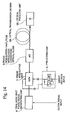
- FIG. 13 is a block diagram showing a further embodiment of the optical transmitter according to the present invention.
- a dual mode beat pulse generating unit 4' is used instead of the LD that generates a single longitudinal mode signal for the optical transmitter shown in FIG. 1 .
- the duty cycle of the RZ pulse signal can be uniform between pulses, and thus the transmission quality can be improved.
- a dual mode beat pulse signal whose repetition frequency is equal to the line rate is generated by the dual mode beat pulse generating unit 4'.
- the details of this unit will be explained below because a structure identical to the two beat generating pulse unit 91 shown in FIG. 41 can be used.
- the mode-locked semiconductor laser that has a two mode oscillation disclosed in citation K. Sato, A Hirano, N. Shimizu, T Ohno, and H Ishii, "Dual mode operation of semiconductor mode-locked lasers for anti-phase pulse generation", OFC'2000, 320/ThW3-1, 2000, can be used.
- the dual mode beat pulse is PSK modulated by the phase modulating unit 3.
- the structure of this unit can be selected from the structures shown in either FIG. 3 or FIG. 7 .
- the pre-coding unit 2 can be structured identically to the pre-coding unit 2 shown in FIG. 35 .
- the connections between the phase modulating unit 3 and the pre-coding unit 2 are identical to those in FIG. 35 when using the phase modulating unit 3 shown in FIG. 2 .
- the advantage of using the dual mode beat pulse generating unit 4' is that the loss in the phase modulation/amplitude modulation converting optical filter used as an optical filter unit 5 is largely decreased in comparison to the case of using a CW light source such as those in FIGS. 1 and 2 .
- the duty cycle of the generated pulse train can be determined by a dual mode beat pulse, and thus fluctuations of the duty cycle due to the input data pattern can be suppressed.
- the tolerance with respect to optical nonlinear effects in the optical fiber can be improved in comparison to using the optical transmitter shown in FIGS. 1 and 2 .
- the advantages that the symmetry of the two generated duobinary optically modulated spectra can be improved, and thus the chromatic dispersion tolerance characteristics can be improved.
- FIG. 14 is a diagram showing another embodiment of the optical transmission system according to the present invention.
- FIGS. 15 , 16 , and 20 are diagrams for explaining the operation thereof.
- the output of the optical transmitter shown in FIG. 13 is input into the optical transmission medium 69.
- a phase modulation/amplitude modulation converting Mach-Zehnder interferometer type optical filter whose delay time is 1 bit is used as an optical filter unit 5.
- a single mode fiber can be used as an example of the optical transmission medium 69.
- a direct detection receiver can be used as an optical receiver 66.
- FIGS. 15A through 15F show the waveforms for each of the parts in FIG. 14 .
- a binary NRZ data electrical signal (line rate B) is input into a pre-coding unit 2.
- a sine wave synchronized with the data signal and having a repetition frequency of B equal to the line rate B is input.
- the dual mode beat pulse signal generating unit 4' generates the dual mode beat pulse having the modulated spectrum shown in FIG. 16A , and inverts the phase thereof for each bit as shown in FIG. 15B .
- this dual mode beat pulse is modulated at the timing such as that in FIG. 15C by the phase modulating unit 3 in FIG. 13 , as shown in FIG. 16B , an optical signal spectrum having an optical modulated band of 3B in which the carrier component is suppressed is output, and thereby the phase modulated RZ signal as shown in FIG. 15D is generated.
- this phase modulated RZ signal is used as a transmission code, the optically modulation band can be reduced in comparison to the technology disclosed in the citation (Miyano et al.). This signal is input into the phase modulation/amplitude modulation converting optical filter used as the optical filter unit 5.
- a Mach-Zehnder interferometer type optical filter whose FSR (free spectral range) is equal to the line rate B can be considered as the phase modulation/amplitude modulation converting optical filter, and the optical signal output from the port (shown by the solid line) having transmittance characteristics in which, as shown in FIG. 16C , the center frequencies of the rejection bands coincide with the carrier frequency f 0 can be considered.
- FIG. 16D as an optical signal spectrum, the DCS-RZ signals in which two optical duobinary signal spectra are arranged at a frequency difference of B can be obtained, and the intensity modulated waveform shown in FIG. 15E can be obtained. The phase of this output optical signal is inverted at each mark bit.
- the optical signal output from a port (shown by the dashed line) having transmittance characteristics such that the center frequencies of the pass bands coincided with the carrier frequency f 0 can be considered.
- a duobinary RZ signals in which three optical duobinary signal spectra are arranged at the frequency difference B as shown in FIG. 16E are obtained, and an intensity modulated waveform such as that shown in FIG. 15F is obtained.
- This output optical signal has phase modulating rules identical to a duobinary signal.
- FIG. 17 shows an embodiment of the optical transmission system using the optical transmitter shown in FIG. 13 . This differs from the embodiment shown in FIG. 14 in that the amount of delay of the pre-coding unit 2 and the amount of delay of the MZI optical filter used as the optical filter unit 5 are selected so that each takes 2 time slots.
- the output of the optical transmitter shown in FIG. 13 is input into the optical transmission medium 69.
- a phase modulation/amplitude modulation converting Mach-Zehnder interferometer type optical filter circuit having a delay time of 2 bits is used as the optical filter unit 5.
- the optical transmission medium 69 a single mode fiber is used.
- a direct detection receiver is used as the optical receiving unit 66.
- FIGS. 18A through 18G show the waveforms for each of the blocks shown in FIG. 17 .
- a binary NRZ data electrical signal (line rate B) is input into the pre-coding unit 2.
- the dual mode beat pulse generating unit 4' shown in FIG. 17 in the case, for example, of using a mode-locked semiconductor laser, a sine wave having a repetition frequency of B that is equal to the line rate B synchronized with the data signal is generated.
- the dual mode beat pulse generating unit 4' generates a dual mode beat pulse having the modulated spectrum as shown in FIG. 19A , and inverts the phase thereof for each bit, as shown in FIG. 18C .
- phase modulating unit 3 shown in FIG. 17 performs phase modulation on this dual mode beat pulse using a pre-coded signal at the timing such as that in FIG. 18B , as shown in FIG. 19B , an optical signal spectrum having the optical modulation band of 3B in which the carrier component is suppressed is output, and a phase modulated RZ signal as shown in FIG. 18D is generated.
- this phase modulated RZ signal is used as a transmission code, the optical modulation band can be reduced in comparison to the technology of the above citation (Miyano et al.). This signal is input into the phase modulation/amplitude modulation converting optical filter that forms the optical filter unit 5.
- a Mach-Zehnder interferometer type optical filter whose FSR is equal to half the line rate B can be considered as the phase modulation/amplitude modulation converting optical filter.
- An optical signal output from a port (shown by the solid line) having transmittance characteristics in which the rejection band center frequencies thereof are arranged equally around the carrier frequency f 0 as shown in FIG. 19C can be considered.
- the optical signal spectrum of this port has a signal spectrum such as that shown in FIG. 19E , and an RZ intensity modulated optical signal such as that shown in FIG. 18G can be obtained.
- an optical signal output from a port (shown by the dashed line) having transmittance characteristics such that the pass band center frequencies are arranged equally at the carrier frequency f 0 as shown in FIG. 19C .
- the optical signal spectrum shown in FIG. 19D is obtained, and the intensity modulated frequency as shown in FIG. 18F is obtained.
- Either of the bandwidths of the RZ signals described above is narrow, respectively equal to or less than 2B or 3B, and it is understood that use the NRZ code can be used as a baseband signal, and the bandwidth-reduced RZ intensity modulated signal in comparison with the conventional code can be generated.
- FIG. 20 is a block diagram showing another embodiment of the optical transmitter according to the present invention.
- the embodiment shown in FIG. 20 differs from the embodiment shown in FIG. 13 in that the optical filter unit 5 for converting phase modulated signals to intensity modulated RZ signals is not present. Therefore, the difference is only that the signal transmitted through the optical transmission medium line (not illustrated) is an RZ intensity modulated phase-encoded signal.
- FIG. 21 is a block diagram showing another embodiment of the optical transmission system according to the present invention using the optical transmitter shown in FIG. 20 .
- This differs from the optical transmission system shown in FIG. 15 in that the phase modulation/amplitude modulation converting optical filter 60 is formed inside the receiver disposed at the output of the optical transmission medium 69.
- a 1-bit delay Mach-Zehnder interferometer type optical filter is used as the phase modulation/amplitude modulation converting optical filter 60, and in the case of considering the frequency setting identical to that of FIG. 16C , the optical output of the two arms of the Mach-Zehnder interferometer type optical filter becomes a complementary optical intensity modulated output signal as shown in FIGS. 15E and 15F .
- the alternating phase modulation by the dual mode beat pulse on the transmitting side does not influence the result of the demodulation of the data.
- the received optical phase modulated RZ signal can be converted to the intensity modulated signal shown in FIG. 15E using the MZI optical filter, and can be received at the normal direct detection receiver.
- the received optical phase modulated RZ signal is converted to the intensity modulated signal shown in FIG. 15F using the MZI optical filter, directly detected and then regenerated, and can be demodulated after inverting the logic thereof. This inversion operation can be carried out at the input of the pre-coding unit 2 of the optical transmitter.
- differential reception of the two outputs shown in FIGS. 16D and 16E can be carried out using two photo detectors.
- the receiver sensitivity when carrying out differential reception can be improved by a 3 dB in comparison to the case where differential reception is not carried out.
- FIG. 23A through FIG. 26C are diagrams for explaining another embodiment of the present invention.
- the optical duobinary component is included in the demodulated intensity modulated signal components. Therefore, as shown in FIGS. 23A, 23I, 23J , 24D, 24G, and 24H , a band pass filter such as the ones in FIGS. 23I and 24G is provided in the receiver, and by direct detection, as shown in FIGS. 23J and 24H , an arbitrary optical duobinary signal component included in the demodulated signal can be obtained, and the chromatic dispersion tolerance can be increased.
- the optical duobinary signal spectrum can be extracted from the signal spectrum of the received optical phase modulated RZ signal by filtering, and thereby, the chromatic dispersion tolerance can be almost doubled in comparison to the case of using the receiver shown in FIG. 22A .
- the optical duobinary component of the upper side band is extracted, but the optical duobinary component of the lower side band can also be extracted.
- the optical duobinary component that includes the carrier frequency is extracted, but either one of the upper or lower optical duobinary components can be extracted.
- the tolerance with respect to the optical nonlinear effects on the optical transmission medium can be improved, and at the receiving side, by carrying out phase modulation/amplitude modulation conversion and then limiting the signal band in the optical carrier frequency domain, the chromatic dispersion tolerance of the transmission line ban be improved.
- FIGS. 25A and 25B are examples of a concrete structure that adds a band limiting function to the optical filter unit and thereby improves the chromatic dispersion tolerance of the demodulated signal.
- the RZ phase modulated signal that is transmitted over the optical transmission medium is amplified by the optical pre-amplifier 251, and then is converted to an intensity modulated signal by the MZI optical filter 252.
- the optical band pass filter 253 having a transfer function that is nearly square, as shown in FIGS. 23I and 24G between the MZI optical filter 252 and the direct detection receiver 254, the optical duobinary component can be extracted.
- FIG. 25B is an example in which the equivalent functions of the MZI filter 252 in FIG. 25A and the band limiting optical band pass filter 253 are realized by one Gaussian filter 255, which is easily realized.
- the RZ phase modulated signal that is transmitted over the optical transmission medium is amplified by the optical pre-amplifier 251, and then the center frequency of the Gaussian filter 255 is matched with the center frequency of the desired optical duobinary component, and the phase modulation/amplitude modulation conversion and the band limiting function can be realized by a single device.
- FIGS. 26A through 26C are diagrams showing a graphical representation of the results of numerical calculation of a concrete experimental example of FIG. 25B .
- FIG. 26A is an example of the calculation in the case of the frequency arrangement shown in FIGS. 23A, 23I, and 23J , and shows with the dashed line the modulated spectrum of an RZ phase modulated signal modulated with a M sequence pseudo-random signal having a line rate of 43 Gbit/s.
- the solid line shows the optical duobinary component extracted by one Gaussian filter whose full width at half maximum is 24 GHz.
- the waveform of the extracted signal that has been directly detected is shown in FIGS. 26B and 26C . According to FIGS.
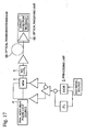
- FIG. 27 is a diagram showing an example of the structure of a phase modulation/amplitude modulation converting optical filter used in the transmitter or the receiver according to the present invention.
- the optical phase modulated signal is input into the port 1 of the circulator 271, and output from the port 2 of the circulator 271.
- the optical phase modulated signal from the port 2 is input into the polarization beam coupler/splitter 272, and separated into two linearly polarized wave components which are orthogonal to each other.
- the polarization axis of one of the optical phase modulated signal components of the split polarization components is rotated by 90°.
- Two polarization separated signals are coupled to either a TE propagation mode or a TM propagation mode of the phase modulation/amplitude modulation converting optical filter.
- the optical signals are propagated together in the opposite directions, and have undergone phase modulation/amplitude modulation conversion with the same transmission mode.
- the converted intensity modulation signal is again input into the polarization beam coupler/splitter 272, is polarization-combined, and then output from the port 1 of the polarization beam coupler/splitter 272, and input into the port 2 of the circulator 271.
- the demodulated intensity modulation signal that has been polarization-combined can be extracted from the port 3 of the circulator.
- phase modulation/amplitude modulation conversion that is not influenced by the polarization sensitivity of the phase modulation/amplitude modulation converting filter can be realized.
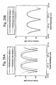
- FIGS. 28A and 28B present as a graph an experimental example of the phase modulation/amplitude modulation converting optical filter in the 1.58 ⁇ m band.
- an MZI interference filter having FSR of 50 GHz formed on a silica waveguide is used as an optical filter.
- FIG. 27 when the input polarization changes, a maximum shift in the transfer function of approximately 9 GHz can be observed.
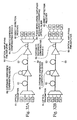
- the optical phase modulating unit 3 comprises two DPSK modulating units 301 and 302 connected in series and the two input data signals can be time division multiplexed in the processing block of the optical carrier frequency band, and this is desirable for the realization of the high speed operation.
- FIGS. 30A to 30J are diagrams for explaining the operation of the transmitter shown in FIG. 29 .
- FIGS. 30A and 30B are two independent multiplexed digital electrical signals D1 and D2 that have the same bit rate, and are binary NRZ signals.
- D1 and D2 are time division multiplexed to generate the binary NRZ multiplexed signal shown in FIG. 30C.
- FIG. 30D shows the data generated by pre-coding this multiplexed signal.
- the signal generated by the DPSK modulation of D1 and D2 using time division multiplexing is phase modulated in conformity to FIG. 30D .
- the optical transmitter shown in FIG. 29 generates the multiplexed phase modulated signal by carrying out the processing using the processing block of the optical carrier frequency band instead of carrying out multiplexing in the baseband.
- FIGS. 30E and 30F are pre-coded NRZ data P1 and P2 that have been obtained by converting D1 and D2 using the pre-coding unit 2 shown in FIG. 35 , and the code is inverted each time a mark bit is input.
- the pre-coded NRZ data P2 is delayed by T/2 (where T is one time slot of the input data signals D1 and D2) as a relative delay difference in comparison to P1.
- the signal INPUT is phase modulated, as shown in FIG. 30E , by the DPSK modulator 301 based on P1, and input into the DPSK modulator 302.
- the DPSK modulators 301 and 302 carry out phase modulation using P2 in accordance with a DPSK format in the manner shown in FIG. 30G at a timing delayed by T/2 in comparison to the phase modulation timing of D1 shown in FIG. 30F .
- the DPSK modulators 301 and 302 output a signal shown in FIG. 30H .
- a phase modulated signal which is the same as the phase modulated signal obtained from one of the DPSK modulator 301 and 302, is generated using the multiplexed data shown in FIG. 30D that is obtained by the time division multiplexing of D1 and D2 and the pre-coding of the multiplexed signal.
- FIG. 30I are combined using a Mach-Zehnder interferometer type modulator, and when phase modulation/amplitude modulation conversion is carried out, as shown in FIG. 30J , a signal has been demodulated that is identical to the original multiplexed signal shown in FIG. 30C .
- FIG. 31 is a block diagram showing yet another embodiment of the pre-coding device (in the case of a 1 bit delay) used in the optical transmitter according to the present invention.
- the embodiment shown is basically the same as the embodiment shown in FIG. 29 , but instead of carrying out exclusive OR of a plurality of delayed pre-coded multiplexed signals in the optical phase modulator using the carrier frequency, this is carried out using the baseband.
- the two synchronized independent NRZ signal 1 and NRZ signal 2 having identical line rates of B are each pre-coded by the pre-coding unit 2 shown in FIG. 35 .
- the delay time of the delay element is set equal to the time slot T 0 of NRZ signal 1 among the multiplexed NRZ 1 and 2 signals.
- One of the pre-coded NRZ signal is delayed by the delay element, the relative delay difference of each of the phase modulation timings is set equal to T 0 /2, and the exclusive OR is processed by the exclusive OR circuit 204.
- the output of this exclusive OR circuit 204 is equal to the pre-coded signal after the NRZ 1 input signal and the NRZ 2 input signal are multiplexed by bit interleaving
- a pre-coding unit 2 which is difficult to operate at high speed, can be realized by performing parallel processing using a pre-coding circuit that operates as a low speed. As a result, increasing the speed of the pre-coding unit 2 can be easily realized.
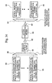
- the optical carrier frequencies (f 01 to f 0n ) of the transmitter are set in agreement with each of the channel grids of the wavelength division multiplexing system shown in FIG. 34.
- FIG. 34 is a diagram showing an embodiment in which the channel spacing is equal.
- the optical carrier signal from the light source 4 is modulated using a DPSK optical modulation format by the MZ optical intensity modulator 32.
- Baseband signal processing by the DPSK optical modulation format is identical to that in FIG. 2 , and thus the explanation thereof is omitted.
- the DPSK optical modulated signals modulated by the optical transmitter for each channel are wavelength division multiplexed by the wavelength-division-multiplexing-light multiplexing filter 80.
- the wavelength division multiplexed DPSK optical modulation code is optically amplified according to necessity, it is input into the optical filter unit 83.
- the rejection band optical center frequency of the optical filter unit 83 is set to the optical carrier frequency of each channel, and in addition, the period thereof is set to the grid period of the wavelength division multiplexed channels.
- the periodic optical filter unit 83 By setting the operating conditions of the optical filter unit 83 in the above manner, the periodic optical filter unit 83 simultaneously converts the wavelength division multiplexing DPSK optical modulated signals to a wavelength division multiplexing DCS-RZ optical modulated signals.
- an MZI type optical filter can be used as an optical filter unit 83.
- the simultaneously converted DCS-RZ optical modulation code is optically amplified by the optical amplifier 62 according to necessity, and input into the optical transmission medium 69 at a predetermined transmission channel power.
- the optical transmission medium 69 can be, for example, a linear repeating transmission line having an optical fiber that is optically directly amplified and repeated by an optical amplifier repeater.
- the output of the optical transmission medium 69 is optically amplified, and then input into the wavelength demultiplexing filter 81, the DSC-RZ code is wavelength demultiplexed by each channel, and input into the optical receiver 65 after wavelength demultiplexing.
- the operation in the optical receiver 65 is identical to that of the embodiment shown in FIG. 12 , and thus the explanation thereof is omitted.
- the transmitter 85 that uses the wavelength division multiplexing transmission scheme, only an example was given in which a plurality of channels are simultaneously converted to RZ intensity modulated signals by the wavelength-division-multiplexing-light multiplexing filter 80, but the same effect can be attained by making the polarization of the adjacent wavelength channels orthogonal.
- FIGS. 36A through 36D are diagrams for explaining the operation of the embodiments shown in FIG. 34 and FIG. 35 .
- the carrier signals ( FIG. 36A ) disposed at equal spacing in the optical frequency domain are each modulated using the DPSK format, and the output of the wavelength-division-multiplexing-light multiplexing filter 80 becomes a wavelength division multiplexed DPSK optical signal spectrum such as that in FIG. 36B .
- the optical filter unit 5, which is one essential component of the present invention, can be realized by using a periodic optical filter 83 such as that in FIG. 36C.
- FIG. 36D shows the optically modulated spectrum of the converted wavelength division multiplexing DCS-RZ code.
- the wavelength division multiplexing DPSK optical signals can be converted simultaneously to wavelength division multiplexing DCS-RZ optical modulated signals.
- the wavelength division multiplexing having equal spacing was assumed in the explanation, but unequal spacing can be used, and in this case, optical filters having equal transfer functions in the optical signal band of the respective channels are used.
- FIG. 37 is a diagram for explaining yet another embodiment of the optical transmission system according to the present invention.
- the transmission format is a phase encoded RZ format using a dual mode beat pulse and that a phase modulation/amplitude modulation converting periodic optical filter 70 is disposed at the receiving end.
- the optical transmission medium can be a linear repeating transmission line having an optical fiber that is optically amplified and repeated by the optical amplifier repeater 62.
- the structures shown in FIGS. 22A through 22C and FIGS. 25A and 25B are used as an optical receiver.
- the optical carrier frequency (f 01 to f 0n ) of the transmitter are set to match each of the channel grids of the wavelength division multiplexing system shown in FIG. 37 .
- FIGS. 38A through 38E show examples in which the wavelengths are equally spaced (3B, which is three times the line rate).
- Each of the optical transmitters can have the structure shown in FIG. 20 .
- the phase modulating unit 3 can be any of the structures shown in FIGS. 2 , 7 , and 29 .
- the baseband processing using the DPSK optical modulation format is identical to that in FIGS. 2 and 29 , and thus the explanation thereof is omitted.
- the DPSK-CS-RZ signals ( FIG. 38 ) modulated by the optical transmitters of respective channels is wavelength division multiplexed by the wavelength-division-multiplexing-light multiplexing filter 81.
- the wavelength division multiplexed DPSK-CS-RZ optical transmission code is optically amplified according to necessity, and then input into the optical transmission medium 69.
- the output of the optical transmission medium 69 is input into the optical phase modulation/amplitude modulation converting periodic optical filter 70.
- the central frequency of the rejection band of the optical phase modulation/amplitude modulation converting periodic optical filter 70 is set to the optical carrier frequency of each of the channels, and in addition, the period thereof is set to the grid period of the wavelength division multiplexed channels.
- FIG. 38A shows the spectrum of the dual mode beat pulse signals generated by each of the optical transmitters in FIG. 37 .
- FIG. 38B shows the spectrum of a signal that is wavelength division multiplexed by the wavelength-division-multiplexing-light multiplexing filter 81 after phase modulating the dual mode beat pulse signal in each of the optical transmitters shown in FIG. 37 .
- a 1-bit delay Mach-Zehnder optical filter is used as the optical periodic filter 70. If the pass band arrangement for the optical periodic filter is selected as shown by the solid line in FIG. 38C , then as shown in FIG. 38D , differential output RZ optical intensity modulated signals are generated by simultaneous conversion, and it is output from the optical periodic filter 70. In addition, if the pass band arrangement is selected as shown by the dashed line in FIG. 38C , then as shown in FIG. 38E , sum output RZ optical intensity modulated signals are generated by simultaneous conversion, and it is output from the optical periodic filter 70.
- One of the above RZ optical intensity modulated signals generated by simultaneous conversion is demultiplexed by wavelength by a wavelength-division-multiplexing-light multiplexing/demultiplexing filter 82, and demodulated at each of the optical receivers.
- the FSR should be set equal to or greater than the line rate B.
- the FSR of the optical phase modulation/amplitude modulation converting periodic optical filter 70 is 50 GHz.
- polarization insensitive optical phase modulation/amplitude modulation converting filter shown in FIG. 27 is preferably used.
- FIG. 39 is a diagram showing an embodiment in the case that the function of the phase modulation/amplitude modulation converting periodic optical filter 70 and the function of the wavelength-division-multiplexing-light multiplexing/demultiplexing filter 82 are realized by one optical filter.
- FIGS. 40A through 40C are diagrams for explaining the conversion operation of the filter shown in FIG. 39 .
- the wavelength division multiplexing RZ phase encoded signal is input into the receiver 66 shown in FIG. 39 after being transmitted over an optical transmission medium such as an optical filter.
- the wavelength division multiplexed signals are amplified together by the optical amplifying pre-amplifiers 62, and input into the wavelength demultiplexer 180.
- the center frequency of the pass band in each of the channels of the wavelength demultiplexer 180 is set to the carrier frequency of each of the channels.
- the wavelength division multiplexing having equal spacing was assumed in the explanation, but unequal spacing can be used.
- the pass band shape of the wavelength demultiplexer is a Gaussian, and its FWHM is set from 0.5 to 0.6 times the channel line rate. In the example shown in FIGS. 26A through 26C , the FWHM is set to 0.56 times the line rate.
- the advantage of this scheme is that realization of optical phase modulation/amplitude modulation converting filter is easy and the loss in the pass band is low.
- a Gaussian filter whose pass band is insensitive to the input polarization can be used.
- the array waveguide grating filter disclosed in the citation, H. Takahashi, K. Oda, H. Toba, and Y. Inoue, "Transmission characteristics of arrayed waveguide N ⁇ N wavelength multiplexer", IEEE J. Lightwave Technol, 13, No. 3, pp. 447-455, 1995 is used, a wavelength division multiplexing demultiplexer using a Gaussian filter having uneven spaces or even spaces can be realized.
- the periodic filter simultaneously converts the wavelength division multiplexing DPSK optical modulated signals to wavelength division multiplexing RZ signals.
- FIGS. 32A, 32B , 33A and 33B are diagrams for explaining the effect of the optical transmission system according to the present invention using the phase modulation format as the transmission format.
- FIGS. 32A and 32B show the models of two computer simulations.
- the computing conditions are as follows: line rate, 43 Gbit/s; number of channels, 4; wavelength division multiplexing channel spacing, 100 GHz; and signal wavelength, C band.
- the fiber transmission line was a 200 km optical amplifier and repeater transmission line, and each span comprised of a 100 km dispersion shifted fiber (loss, 0.21 dB; dispersion value, +2ps/nm/km; dispersion slope, 0.07 ps/km/nm).
- the dispersion of the first span is compensated by the optical amplifier repeater such that the center wavelengths of channel 2 and channel 3 have zero dispersion, and the output of the first span is input into the second span.
- FIG. 32A A calculation model ( FIG. 32A ) in which an RZ format that carries out phase modulation/amplitude modulation conversion in the transmitter as shown in FIG. 14 is used, is compared with a calculation model ( FIG. 32B ) in which an RZ format that carries out phase modulation/amplitude modulation conversion in the receiver as shown in FIG. 21 is used.
- Each of the optical carrier signals is modulated by the optical transmitter 61 shown in FIG. 13 or FIG. 20 , then wavelength division multiplexed by a wavelength division multiplexing filter at a 100 GHz spacing, and input into the fiber transmission line 63.
- the output of the fiber transmission line 63 is optically amplified, demultiplexed by wavelength, and then the chromatic dispersion of the transmission line is compensated by the chromatic dispersion compensating device D (64).
- the signal received by the direct detection receiver 66 is regenerated.
- the dispersion compensated optical signal is input into the MZI filter, which serves as the phase modulation/amplitude modulation converting optical filter 60, and after being converted to an intensity modulated signal, the signal received by the direct detection receiver 66 is regenerated.
- FIG. 33A shows for each of the channels the tolerance range of the eye opening penalty within 1 dB in the case that the channel power and the total dispersion (i.e., the total of the dispersion of the fiber transmission line and the dispersion of the dispersion compensating device D) change for the structure shown in FIG. 32A .
- the dispersion tolerance of each of the channels becomes about 80 ps/nm, which is almost twice that of the dispersion tolerance in comparison with normal RZ format can be realized.
- the RZ format transmission scheme described above has a wide dispersion tolerance.
- the allowable channel power for which the transmission characteristics for all channels remain within an eye opening penalty of 1 dB is determined by channels 2 and 3, and is approximately +5 dBm.
- FIG. 33B shows for each of the channels the tolerance range of the eye opening penalty within 1 dB in the case that the channel power and the total dispersion (i.e., the total of the dispersion of the fiber transmission line and the dispersion of the dispersion compensating device D) changes for the structure shown in FIG. 32B .
- the dispersion tolerance of each of the channels becomes about 80 ps/nm, which is almost twice that of the normal RZ format, and a dispersion tolerance equivalent to the case shown in FIG. 32A can be realized.
- the RZ format transmission scheme described above has a wide dispersion tolerance in comparison to conventional technology.
- allowable channel power for which the transmission characteristics for all channels remain within an eye opening penalty of 1 dB is determined by channels 2 and 3, and is approximately +8 dBm.
- the allowable channel power can be improved by approximately 3 dB over that of the scheme shown in FIG. 32A , and the tolerance with respect to degradation due to non-linear effects can be improved. Furthermore, because the optimal dispersion value does not depend on the channel power, an optical amplifier repeater system whose channel power has a wide dynamic range can be realized using a wavelength division multiplexing technology.
Claims (19)
- Transmetteur optique adapté pour générer un signal optique RZ à porteuse supprimée duobinaire, ledit transmetteur comprenant :une source de lumière de mode longitudinal unique (4) adaptée pour générer un signal optique de mode longitudinal unique ;un dispositif de précodage (2) adapté pour recevoir un signal NRZ et générer un signal NRZ précodé ou un signal NRZ précodé différentiel dont la logique s'inverse à chaque fois qu'un bit de marque est entré ; etun dispositif de modulation de phase optique (3) adapté pour moduler la phase optique du signal optique de mode longitudinal unique en utilisant le signal NRZ précodé ou le signal NRZ précodé différentiel, et adapté pour délivrer un signal optique modulé DPSK ;caractérisé en ce que le transmetteur comprend en outre :un dispositif de filtrage optique (5) adapté pour convertir le signal optique modulé DPSK en un signal optique modulé en intensité RZ, et adapté pour délivrer le signal optique modulé en intensité RZ, et adapté pour avoir une fréquence centrale de bande de réjection qui correspond à la fréquence de porteuse optique du signal optique modulé DPSK.
- Transmetteur optique selon la revendication 1, dans lequel un modulateur d'intensité optique Mach-Zehnder est utilisé en tant que dispositif de modulation de phase optique (3), dans lequel une polarisation continue est appliquée au modulateur d'intensité optique Mach-zehnder de manière à obtenir une transmission nulle en l'absence de modulation, et le modulateur d'intensité optique Mach-Zehnder applique la modulation par déplacement de phase différentielle au signal optique de mode longitudinal unique en utilisant le signal NRZ précodé ou le signal NRZ précodé différentiel.
- Transmetteur optique selon la revendication 1 ou 2, dans lequel le dispositif de filtrage optique (5) est un filtre optique du type interféromètre Mach-Zehnder.
- Transmetteur optique selon la revendication 1, dans lequel le dispositif de filtrage optique (5) est un filtre optique du type interféromètre Mach-Zehnder dont la fréquence centrale de bande de réjection coïncide avec la fréquence de porteuse d'un canal, et dont le champ de signal optique de sortie est :

où l'amplitude du champ de signal optique d'entrée est désignée par Ein, la fréquence optique est désignée par ω, la quantité de retard d'un élément à retard est désignée par τ, et la phase relative entre les signaux optiques qui se sont propagés à travers deux guides d'onde dans le filtre optique du type interféromètre Mach-Zehnder est désignée par φ. - Transmetteur optique selon la revendication 3 ou 4, dans lequel la différence de retard relative entre deux branches du filtre optique du type interféromètre Mach-Zehnder est d'une tranche de temps.
- Transmetteur optique adapté pour générer un signal optique RZ duobinaire ou un signal optique RZ à porteuse supprimée duobinaire, ledit transmetteur comprenant :une source de lumière impulsionnelle à battement de mode double (4') adaptée pour générer deux signaux de mode longitudinal qui se synchronisent avec un signal de données et qui ont un espacement de mode entre les deux signaux de mode longitudinal qui est un multiple entier d'un débit de ligne de données, et qui sont verrouillés en mode l'un avec l'autre ;un dispositif de précodage (2) adapté pour recevoir un signal NRZ pour effectuer une conversion de code, et pour délivrer un signal NRZ précodé ou un signal NRZ précodé différentiel ; etun dispositif de modulation de phase optique (3) adapté pour moduler la phase optique d'un train d'impulsions optiques généré par la source de lumière impulsionnelle à battement de mode double en utilisant le signal NRZ précodé ou le signal NRZ précodé différentiel, et adapté pour délivrer un signal modulé DPSK-CSRZ ;caractérisé en ce que le transmetteur comprend en outre :un dispositif de filtrage optique (5) adapté pour convertir un signal modulé DPSK CS-RZ généré par le dispositif de modulation de phase optique (3) en un signal optique modulé en intensité RZ ayant soit la même logique, soit la logique inversée du signal NRZ, et adapté pour délivrer le signal optique modulé en intensité RZ.
- Transmetteur optique selon la revendication 6, dans lequel le dispositif de précodage (2) effectue un précodage différentiel en appliquant un traitement OU exclusif au signal NRZ qui est appliqué au dispositif de précodage et à un signal NRZ retardé, et le dispositif de précodage génère le signal NRZ retardé en retardant le signal NRZ obtenu par le traitement OU exclusif de n bits, où n est un nombre entier naturel.
- Transmetteur optique selon la revendication 6, dans lequel le dispositif de filtrage optique (5) est un filtre optique du type interféromètre Mach-Zehnder, et la différence de retard relative entre deux branches dans le filtre optique du type interféromètre Mach-Zehnder est supérieure à n-1 bits et inférieure à n+1 bits, où n est un nombre entier naturel.
- Système de transmission optique comprenant :un transmetteur optique (61) selon les revendications 1 ou 6 ;un support de transmission optique (69) adapté pour transmettre le signal optique modulé en intensité RZ délivré par le transmetteur optique (61) ; etun récepteur optique (66) adapté pour recevoir le signal optique modulé en intensité RZ délivré par le transmetteur optique (61) par l'intermédiaire du support de transmission optique (69), et pour démoduler et détecter directement le signal optique modulé en intensité RZ pour convertir le signal optique modulé en intensité RZ en un signal électrique de bande de base.
- Système de transmission optique selon la revendication 9, dans lequel le récepteur optique (66) compense la distorsion de forme d'onde, qui est induite dans le signal optique modulé en intensité RZ, due à une dispersion chromatique ou à une dispersion de mode de polarisation du support de transmission optique (69).
- Système de transmission optique selon la revendication 9, dans lequel les signaux optiques modulés DPSK sont générés par le dispositif de modulation de phase optique (3) dans le transmetteur optique (61), sont multiplexés par répartition en longueur d'onde, et sont ensuite convertis simultanément en les signaux optiques modulés en intensité RZ multiplexés par répartition en longueur d'onde par le dispositif de filtrage optique (5) unique du transmetteur optique (61), et transmis par l'intermédiaire du support de transmission optique (69).
- Système de transmission optique selon l'une quelconque des revendications 9 à 11, dans lequel le système de transmission optique est un système de transmission à multiplexage par répartition en longueur d'onde, et un filtre optique périodique dont la plage spectrale libre est égale à l'espacement des canaux de multiplexage par répartition en longueur d'onde du système de transmission à multiplexage par répartition en longueur d'onde est utilisé en tant que dispositif de filtrage optique (5).
- Système de transmission optique selon l'une quelconque des revendications 9 à 11, dans lequel le système de transmission optique est un système de transmission à multiplexage par répartition en longueur d'onde, et un filtre optique ayant une fonction de transfert identique dans la bande de signal optique pour chacun des canaux du système de transmission à multiplexage par répartition en longueur d'onde est utilisé en tant que dispositif de filtrage optique (5).
- Système de transmission optique selon l'une quelconque des revendications 9 à 11, dans lequel le système de transmission optique est un système de transmission à multiplexage par répartition en longueur d'onde, et la polarisation des canaux de multiplexage par répartition en longueur d'onde contigus du système de transmission à multiplexage par répartition en longueur d'onde est orthogonale.
- Transmetteur optique selon l'une quelconque des revendications 1 à 8,
dans lequel le dispositif de modulation de phase optique (3) dans le transmetteur optique (61) comprend n modulateurs DPSK (301, 302), où n est un nombre entier naturel, connectés en sérine ; et
dans lequel le signal de commande du mème modulateur DPSK est généré par un dispositif à retard (203) adapté pour retarder le mème signal d'entrée du dispositif de modulation de phase optique d'un intervalle égal à (m-1)/(nB), où m est un nombre entier naturel, et par un dispositif de précodage (201, 202) adapté pour précoder le signal modulé retardé, et
dans lequel les modulateurs DPSK convertissent n signaux modulés de bande de base multiplexés ayant un débit binaire B en un signal optique modulé multiplexé par répartition dans le temps ayant un débit de ligne nB. - Transmetteur optique selon l'une quelconque des revendications 1 à 6, la revendication 8, et la revendication 15,
dans lequel le dispositif de filtrage optique (5) est pourvu : d'un diviseur de faisceau par polarisation (272) qui est connecté à un circulateur (271) comportant trois ports ; de dispositifs de préservation de polarisation (275, 276) adaptés pour maintenir l'état de polarisation des deux sorties optiques du diviseur de faisceau par polarisation (272) ; et d'un filtre du type interféromètre Mach-Zehnder adapté pour coupler l'entrée de celui-ci et la sortie de celui-ci,
dans lequel un signal optique d'entrée est appliqué à un premier port du circulateur (271) et est délivré à partir d'un deuxième port du circulateur, et le signal de sortie du circulateur est appliqué à un premier port, qui est un port de multiplexage/démultiplexage, du diviseur de faisceau par polarisation (272), et les signaux optiques délivrés à partir des deuxième et troisième ports du diviseur de faisceau par polarisation (272), qui servent en tant que ports de sortie de séparation de polarisation, sont appliqués aux dispositifs de préservation de polarisation (275, 276), et tout en préservant la polarisation des deux faisceaux de sortie séparés, les faisceaux de sortie séparés sont appliqués dans les directions opposées aux deux ports du filtre optique du type interféromètre Mach-Zehnder de sorte que les deux faisceaux de sortie séparés sont couplés soit au mode TE, soit au mode TM du filtre optique du type interféromètre Mach-Zehnder, et de ce fait un signal optique de sortie provenant d'un troisième port du circulateur (271) est obtenu. - Transmetteur optique selon l'une quelconque des revendications 1 à 8, dans lequel le dispositif de précodage (2) est pourvu : de n circuits de précodage (201, 202) adaptés pour fonctionner au débit de ligne B ; d'un circuit à retard (203) adapté pour retarder chaque sortie des n circuits de précodage (201, 202) de mT0/n, où T0 = 1/B, et m est un nombre entier naturel sélectionné de 1 à n ; et d'un circuit OU exclusif (204) adapté pour traiter le OU exclusif des n signaux de sortie précodés retardés, et dans lequel un signal précodé multiplexé par répartition dans le temps ayant un débit de ligne nB est généré.
- Système de transmission optique selon l'une quelconque des revendications 9 à 14,
dans lequel le dispositif de modulation de phase optique (3) prévu dans le transmetteur optique comprend n, où n est un nombre entier naturel, modulateurs DPSK (301, 302) connectés en série,
dans lequel le signal de commande du mème modulateur DPSK est généré par un dispositif à retard (203) adapté pour retarder le mème signal d'entrée du dispositif de modulation de phase optique d'un intervalle égal à (m-1)/(n3), où m est un nombre entier naturel, et par un dispositif de précodage (201, 202) adapté pour précoder le signal modulé retardé, et
dans lequel les modulateurs DPSK convertissent n signaux modulés de bande de base multiplexés ayant un débit binaire B en des signaux optiques modulés multiplexés par répartition dans le temps ayant un débit de ligne nB. - Système de transmission optique selon l'une quelconque des revendications 9 à 14 et 18,
dans lequel le dispositif de filtrage optique (5) est pourvu : d'un diviseur de faisceau par polarisation (272) connecté à un circulateur (271) comportant 3 ports ; de dispositifs de préservation de polarisation (275, 276) adaptés pour maintenir l'état de polarisation des deux sorties optiques du diviseur de faisceau par polarisation (272) ; et d'un filtre optique du type interféromètre Mach-Zehnder adapté pour coupler l'entrée de celui-ci et la sortie de celui-ci, et
dans lequel un signal optique d'entrée est appliqué à un premier port du circulateur (271) et délivré à partir d'un deuxième port du circulateur, et le signal de sortie du circulateur est appliqué à un premier port, qui est un port de multiplexage, du diviseur de faisceau par polarisation (272), les signaux optiques délivrés à partir des deuxième et troisième ports du diviseur de faisceau par polarisation (272), qui servent en tant que ports de sortie de séparation de polarisation, sont appliqués aux dispositifs de préservation de polarisation (275, 276), et tout en préservant la polarisation des deux faisceaux de sortie séparés, les faisceaux de sortie séparés sont appliqués dans les directions opposées aux deux ports du filtre optique du type interféromètre Mach-Zehnder de sorte que les deux faisceaux de sortie séparés sont couplés soit au mode TE, soit au mode TM du filtre optique du type interféromètre Mach-Zehnder, et de ce fait un signal optique de sortie provenant d'un troisième port du circulateur (271) est obtenu.
Priority Applications (1)
| Application Number | Priority Date | Filing Date | Title |
|---|---|---|---|
| EP10152077A EP2175574B1 (fr) | 2001-06-29 | 2002-06-28 | Système de transmission optique comprenant un émetteur optique du type CS-RZ DPSK |
Applications Claiming Priority (4)
| Application Number | Priority Date | Filing Date | Title |
|---|---|---|---|
| JP2001199467 | 2001-06-29 | ||
| JP2001199467 | 2001-06-29 | ||
| JP2002040855A JP4278332B2 (ja) | 2001-06-29 | 2002-02-18 | 光送信器および光伝送システム |
| JP2002040855 | 2002-02-18 |
Related Child Applications (1)
| Application Number | Title | Priority Date | Filing Date |
|---|---|---|---|
| EP10152077.3 Division-Into | 2010-01-29 |
Publications (3)
| Publication Number | Publication Date |
|---|---|
| EP1271808A2 EP1271808A2 (fr) | 2003-01-02 |
| EP1271808A3 EP1271808A3 (fr) | 2006-04-05 |
| EP1271808B1 true EP1271808B1 (fr) | 2010-05-26 |
Family
ID=26617909
Family Applications (2)
| Application Number | Title | Priority Date | Filing Date |
|---|---|---|---|
| EP10152077A Expired - Lifetime EP2175574B1 (fr) | 2001-06-29 | 2002-06-28 | Système de transmission optique comprenant un émetteur optique du type CS-RZ DPSK |
| EP02291611A Expired - Lifetime EP1271808B1 (fr) | 2001-06-29 | 2002-06-28 | Emetteur optique et système de transmission optique |
Family Applications Before (1)
| Application Number | Title | Priority Date | Filing Date |
|---|---|---|---|
| EP10152077A Expired - Lifetime EP2175574B1 (fr) | 2001-06-29 | 2002-06-28 | Système de transmission optique comprenant un émetteur optique du type CS-RZ DPSK |
Country Status (5)
| Country | Link |
|---|---|
| US (1) | US7116917B2 (fr) |
| EP (2) | EP2175574B1 (fr) |
| JP (1) | JP4278332B2 (fr) |
| CN (2) | CN101064567B (fr) |
| DE (1) | DE60236484D1 (fr) |
Families Citing this family (117)
| Publication number | Priority date | Publication date | Assignee | Title |
|---|---|---|---|---|
| US6556326B2 (en) * | 1996-12-20 | 2003-04-29 | Tyco Telecommunications (Us) Inc. | Synchronous amplitude modulation for improved performance of optical transmission systems |
| US20040161245A1 (en) * | 1996-12-20 | 2004-08-19 | Bergano Neal S. | Synchronous amplitude modulation for improved performance of optical transmission systems |
| US7173551B2 (en) * | 2000-12-21 | 2007-02-06 | Quellan, Inc. | Increasing data throughput in optical fiber transmission systems |
| US7149256B2 (en) * | 2001-03-29 | 2006-12-12 | Quellan, Inc. | Multilevel pulse position modulation for efficient fiber optic communication |
| US7307569B2 (en) * | 2001-03-29 | 2007-12-11 | Quellan, Inc. | Increasing data throughput in optical fiber transmission systems |
| EP1384338B1 (fr) * | 2001-04-04 | 2010-12-15 | Quellan, Inc. | Procede et systeme permettant de decoder des signaux multiniveau |
| US20030030873A1 (en) * | 2001-05-09 | 2003-02-13 | Quellan, Inc. | High-speed adjustable multilevel light modulation |
| US20030007216A1 (en) * | 2001-06-21 | 2003-01-09 | Chraplyvy Andrew Roman | Long haul transmission in a dispersion managed optical communication system |
| US20030090768A1 (en) * | 2001-08-01 | 2003-05-15 | Xiang Liu | Long haul optical communication system |
| US6643046B2 (en) * | 2001-09-26 | 2003-11-04 | Kabushiki Kaisha Toshiba | Apparatus and method for optical modulation |
| ITRM20020056A1 (it) * | 2002-02-04 | 2003-08-04 | Mario Zitelli | Modulazione combinata di intensita' e fase in un sistema di comunicazione ottico. |
| US7212580B2 (en) * | 2002-02-15 | 2007-05-01 | Quellan, Inc. | Multi-level signal clock recovery technique |
| US7095274B2 (en) * | 2002-03-15 | 2006-08-22 | Seiko Epson Corporation | System for demodulation of phase shift keying signals |
| JP2005521298A (ja) * | 2002-03-15 | 2005-07-14 | セイコーエプソン株式会社 | デジタル位相変調(psk)信号をデジタル振幅変調(ask)信号に変換するためのシステムとその方法 |
| JP3892326B2 (ja) * | 2002-03-26 | 2007-03-14 | 富士通株式会社 | 光変調器の制御装置 |
| US6671077B2 (en) * | 2002-04-16 | 2003-12-30 | Lucent Technologies Inc. | Method and apparatus for generating return-to-zero modulated optical signals |
| US20030198478A1 (en) * | 2002-04-23 | 2003-10-23 | Quellan, Inc. | Method and system for generating and decoding a bandwidth efficient multi-level signal |
| JP2004013681A (ja) * | 2002-06-10 | 2004-01-15 | Bosu & K Consulting Kk | 名刺情報管理システム |
| US6963685B2 (en) * | 2002-07-09 | 2005-11-08 | Daniel Mahgerefteh | Power source for a dispersion compensation fiber optic system |
| US7035361B2 (en) * | 2002-07-15 | 2006-04-25 | Quellan, Inc. | Adaptive noise filtering and equalization for optimal high speed multilevel signal decoding |
| JP2004096653A (ja) | 2002-09-04 | 2004-03-25 | Nec Corp | 光送信器及びそれに用いる光変調方法 |
| KR100469725B1 (ko) * | 2002-09-30 | 2005-02-02 | 삼성전자주식회사 | 듀오바이너리 광 송신장치 |
| KR100493095B1 (ko) * | 2002-10-16 | 2005-06-02 | 삼성전자주식회사 | 광 전송 시스템 |
| KR100492971B1 (ko) * | 2002-10-31 | 2005-06-07 | 삼성전자주식회사 | 듀오바이너리 광 전송장치 |
| US7796885B2 (en) * | 2002-11-05 | 2010-09-14 | Lightfleet Corporation | Distribution optical elements and compound collecting lenses for broadcast optical interconnect |
| US7934144B2 (en) * | 2002-11-12 | 2011-04-26 | Quellan, Inc. | High-speed analog-to-digital conversion with improved robustness to timing uncertainty |
| KR100536906B1 (ko) * | 2003-03-19 | 2005-12-16 | 한국전자통신연구원 | 씨에스-알젯 광신호 발생장치 |
| GB0308951D0 (en) * | 2003-04-17 | 2003-05-28 | Azea Networks Ltd | Top-flat spectrum data format for Nx40 Gbit/s WDM transmission with 0.8 bit/s/Hz spectral efficiency |
| US7505695B2 (en) | 2003-04-23 | 2009-03-17 | Mitsubishi Denki Kabushiki Kaisha | Optical receiver and optical transmission system |
| US20040240888A1 (en) * | 2003-05-30 | 2004-12-02 | Juerg Leuthold | System and method for alternate mark inversion and duobinary optical transmission |
| US7277644B2 (en) * | 2003-06-13 | 2007-10-02 | The Regents Of The University Of California | Fade-resistant forward error correction method for free-space optical communications systems |
| DE10329459A1 (de) | 2003-07-01 | 2005-01-20 | Marconi Communications Gmbh | Sender für ein optisches Nachrichtensignal |
| GB2421674B (en) * | 2003-08-07 | 2006-11-15 | Quellan Inc | Method and system for crosstalk cancellation |
| US7804760B2 (en) * | 2003-08-07 | 2010-09-28 | Quellan, Inc. | Method and system for signal emulation |
| KR100566195B1 (ko) | 2003-08-27 | 2006-03-29 | 삼성전자주식회사 | 반도체 광 증폭기를 이용한 듀오바이너리 광 전송장치 |
| US7603045B2 (en) * | 2003-08-28 | 2009-10-13 | Fujitsu Limited | Method and system for automatic feedback control for fine tuning a delay interferometer |
| KR100532305B1 (ko) * | 2003-09-09 | 2005-11-29 | 삼성전자주식회사 | 듀오바이너리 광 송신기 |
| KR100557111B1 (ko) * | 2003-09-16 | 2006-03-03 | 삼성전자주식회사 | 듀오바이너리 광 전송장치 |
| EP1528697A1 (fr) * | 2003-10-30 | 2005-05-04 | Alcatel | Emetteur optique utilisant la modulation RZ-DPSK |
| AU2003276315A1 (en) * | 2003-11-07 | 2005-05-26 | Asperation Oy | All-optical signal processing method and device |
| KR100539893B1 (ko) * | 2003-11-12 | 2005-12-28 | 삼성전자주식회사 | 고밀도 파장분할다중화방식 광전송 시스템을 위한 광 송신기 |
| DE602004030032D1 (de) | 2003-11-17 | 2010-12-23 | Quellan Inc | Verfahren und system zur löschung von antennenstörungen |
| GB0327605D0 (en) * | 2003-11-27 | 2003-12-31 | Azea Networks Ltd | Method and apparatus for producing chirped RZ-DPSK modulated optical signals |
| KR100592878B1 (ko) * | 2003-12-18 | 2006-06-23 | 한국전자통신연구원 | 전기적으로 대역 제한된 광학적 디피에스케이(dpsk)변조 장치 및 방법 |
| FR2864261A1 (fr) * | 2003-12-19 | 2005-06-24 | France Telecom | Dispositif de regeneration d'un signal optique, utilisation d'un tel dispositif et installation comportant un tel dispositif |
| US7616700B2 (en) * | 2003-12-22 | 2009-11-10 | Quellan, Inc. | Method and system for slicing a communication signal |
| US7844186B2 (en) | 2004-02-20 | 2010-11-30 | Alcatel-Lucent Usa Inc. | Method and apparatus for optical transmission |
| US20050201762A1 (en) * | 2004-03-12 | 2005-09-15 | Moeller Lothar Benedict E.J. | Optical RZ-duobinary transmission system with narrow bandwidth optical filter |
| JP4494401B2 (ja) * | 2004-03-17 | 2010-06-30 | 日本電信電話株式会社 | 光伝送システム、光伝送システムの光送信装置及び光受信装置 |
| ATE347197T1 (de) * | 2004-04-08 | 2006-12-15 | Cit Alcatel | Verfahren zur übertragung von digitalen signalen über ein optisches übetragungssystem |
| EP1585235A1 (fr) * | 2004-04-08 | 2005-10-12 | Alcatel | Méthode de transmission de signaux numériques dans un système de transmission optique |
| KR100545778B1 (ko) * | 2004-05-24 | 2006-01-24 | 광주과학기술원 | 유리수차 조화 모드-잠김 반도체 광섬유 레이저 내에서의펄스 진폭 균등화 장치 및 방법 |
| US7346283B2 (en) * | 2004-06-30 | 2008-03-18 | Lucent Technologies Inc. | Method and apparatus for CRZ-DQPSK optical signal generation |
| WO2006013928A1 (fr) * | 2004-08-04 | 2006-02-09 | The Furukawa Electric Co., Ltd. | Dispositif a circuit optique |
| US20080225375A1 (en) * | 2004-09-07 | 2008-09-18 | Raytheon Company | Optically frequency generated scanned active array |
| KR100680815B1 (ko) * | 2004-11-09 | 2007-02-08 | 한국과학기술원 | Fp- ld의 상호 주입을 이용한 광대역 비간섭성 광원을주입하여 파장 고정된 fp- ld의 광 변조방법 및 그시스템 |
| US7522883B2 (en) * | 2004-12-14 | 2009-04-21 | Quellan, Inc. | Method and system for reducing signal interference |
| US7725079B2 (en) * | 2004-12-14 | 2010-05-25 | Quellan, Inc. | Method and system for automatic control in an interference cancellation device |
| DE102005001678B3 (de) * | 2005-01-13 | 2006-06-22 | Siemens Ag | Empfänger für ein optisches differenzphasenmoduliertes Signal |
| JP2008530900A (ja) * | 2005-02-08 | 2008-08-07 | エイジェンシー フォー サイエンス, テクノロジー アンド リサーチ | 光mskデータフォーマット |
| JP4675796B2 (ja) * | 2005-02-15 | 2011-04-27 | 日本電信電話株式会社 | 自動分散補償型光伝送システム |
| US7734190B2 (en) * | 2005-02-24 | 2010-06-08 | Futurewei Technologies, Inc. | System and method for generating optical return-to-zero signals with differential bi-phase shift |
| US7606501B2 (en) | 2005-02-25 | 2009-10-20 | Futurewei Technologies, Inc. | System and method for generating optical return-to-zero signals with alternating bi-phase shift and frequency chirp |
| JP4548236B2 (ja) * | 2005-06-17 | 2010-09-22 | 沖電気工業株式会社 | 光信号受信装置 |
| US7398022B2 (en) * | 2005-07-08 | 2008-07-08 | Mario Zitelli | Optical return-to-zero phase-shift keying with improved transmitters |
| JP4516907B2 (ja) * | 2005-08-26 | 2010-08-04 | 富士通株式会社 | 光受信装置およびその制御方法 |
| US7486896B2 (en) * | 2005-09-07 | 2009-02-03 | Luxdyne Oy | Optical clock recovery |
| US7558486B2 (en) * | 2005-09-28 | 2009-07-07 | Alcatel-Lucent Usa Inc. | All-optical methods and systems |
| WO2007040247A1 (fr) * | 2005-10-05 | 2007-04-12 | Nec Corporation | Récepteur optique, système de communication optique et procédé |
| JP4695500B2 (ja) | 2005-12-02 | 2011-06-08 | 富士通株式会社 | 信号再生装置,光受信装置および信号処理方法 |
| DE502007001357D1 (de) * | 2006-03-03 | 2009-10-01 | Nokia Siemens Networks Gmbh | Modulatoreinrichtung zur erzeugung eines mit einem binärsignal modulierten optischen übertragungssignals |
| US7817924B2 (en) * | 2006-03-24 | 2010-10-19 | The Mitre Corporation | Rate adjustable differential phase shift key (DPSK) modulation |
| US9252983B2 (en) * | 2006-04-26 | 2016-02-02 | Intersil Americas LLC | Method and system for reducing radiated emissions from a communications channel |
| WO2007148377A1 (fr) | 2006-06-19 | 2007-12-27 | Fujitsu Limited | Processeur de signal optique |
| JP4975385B2 (ja) * | 2006-06-30 | 2012-07-11 | シャープ株式会社 | 検波器、偏光制御光学部品及び位相変調光通信システム |
| US8503568B1 (en) * | 2006-09-07 | 2013-08-06 | The Boeing Company | Differential encoding for multiplexed data streams |
| EP1919105B1 (fr) * | 2006-11-06 | 2009-05-13 | Fujitsu Limited | Transmetteur optique et système de transmission optique |
| US7778360B2 (en) * | 2007-01-09 | 2010-08-17 | Fujitsu Limited | Demodulating a signal encoded according to ASK modulation and PSK modulation |
| US8238757B2 (en) * | 2007-01-18 | 2012-08-07 | Futurewei Technologies, Inc. | Method and apparatus for generating optical duobinary signals with enhanced receiver sensitivity and spectral efficiency |
| JP5445943B2 (ja) | 2007-03-06 | 2014-03-19 | 日本電気株式会社 | 光接続装置 |
| JP4927617B2 (ja) * | 2007-03-30 | 2012-05-09 | 株式会社日立製作所 | データ伝送装置および伝送符号の生成方法 |
| CN101150370A (zh) * | 2007-04-12 | 2008-03-26 | 中兴通讯股份有限公司 | Rz-dpsk调制光信号产生装置及方法 |
| WO2009025687A2 (fr) * | 2007-05-04 | 2009-02-26 | Massachusetts Institute Of Technology | Procédé et appareil permettant de transmettre des signaux optiques |
| WO2009004244A1 (fr) * | 2007-06-19 | 2009-01-08 | France Telecom | Reseau optique passif bidirectionnel a haut debit, central optique et dispositif de terminaison de ligne associes |
| JP4838775B2 (ja) * | 2007-07-20 | 2011-12-14 | Nttエレクトロニクス株式会社 | 光送信回路 |
| CN101459470A (zh) * | 2007-12-14 | 2009-06-17 | 华为技术有限公司 | 光传输系统、装置和方法 |
| JP2009171135A (ja) | 2008-01-15 | 2009-07-30 | Nec Corp | 光送信器、光伝送システム及び変調方式選択方法 |
| JP2011129961A (ja) * | 2008-02-19 | 2011-06-30 | Nec Corp | 光送信方法および装置 |
| US8472812B2 (en) * | 2008-02-22 | 2013-06-25 | Nec Corporation | Optical communication system, optical communication method and optical communication apparatus |
| TWI383599B (zh) * | 2008-06-02 | 2013-01-21 | Univ Nat Taiwan | 雙二位元式收發器 |
| CN101860500B (zh) * | 2009-04-13 | 2013-10-09 | 华为技术有限公司 | 一种产生、接收相位偏振调制信号的方法、装置和系统 |
| GB201014115D0 (en) * | 2010-08-24 | 2010-10-06 | Oclaro Technology Plc | Optoelectronic devices |
| JP2012119836A (ja) * | 2010-11-30 | 2012-06-21 | Fuji Xerox Co Ltd | 送信装置及び送受信装置 |
| US8463131B1 (en) * | 2010-12-15 | 2013-06-11 | The Boeing Company | Method and apparatus for conveying timing information |
| US8781336B1 (en) * | 2011-02-10 | 2014-07-15 | Finisar Corporation | Optical filter for use in a laser transmitter |
| EP2541810B1 (fr) * | 2011-06-29 | 2014-09-24 | Alcatel Lucent | Procédé de démodulation d'un signal optique à modulation de phase |
| WO2013064158A1 (fr) * | 2011-11-03 | 2013-05-10 | Iptronics A/S | Récepteur optique rapide |
| CN102523048B (zh) * | 2011-12-15 | 2014-08-27 | 华中科技大学 | 一种光纤非线性效应抑制装置 |
| US20130177316A1 (en) * | 2012-01-06 | 2013-07-11 | Emcore Corporation | Optical communication system, and transmitter and receiver apparatus therefor |
| US8897654B1 (en) * | 2012-06-20 | 2014-11-25 | The United States Of America As Represented By The Administrator Of The National Aeronautics And Space Administration | System and method for generating a frequency modulated linear laser waveform |
| JP2014007578A (ja) * | 2012-06-25 | 2014-01-16 | Mitsubishi Electric Corp | 光送信機 |
| US9374260B2 (en) | 2013-11-07 | 2016-06-21 | Futurewei Technologies, Inc. | Method and apparatus for directly detected optical transmission systems based on carrierless amplitude-phase modulation |
| CN103873182B (zh) * | 2014-03-13 | 2016-06-29 | 华南师范大学 | 一种波分复用数字通信实验教学系统 |
| JP6353398B2 (ja) * | 2015-04-28 | 2018-07-04 | 日本電信電話株式会社 | 光変調回路 |
| CN104869092B (zh) * | 2015-06-02 | 2018-09-11 | 武汉邮电科学研究院 | 基于相干检测和数字信号处理的数字载波再生系统及方法 |
| CN105072058B (zh) * | 2015-08-25 | 2018-05-25 | 许继集团有限公司 | 一种基于光纤传输的数据正反相位编码方法及数据传输方法 |
| JP6681217B2 (ja) * | 2016-02-29 | 2020-04-15 | 日本ルメンタム株式会社 | 光情報伝送システム、及び光送信器 |
| JP2018074057A (ja) * | 2016-11-01 | 2018-05-10 | 住友電工デバイス・イノベーション株式会社 | 半導体レーザキャリア組立体、光半導体装置、及び光半導体装置の製造方法 |
| CN108429713B (zh) * | 2017-02-13 | 2020-06-16 | 大唐移动通信设备有限公司 | 一种数据压缩方法及装置 |
| CN108599867B (zh) * | 2018-03-29 | 2021-02-02 | 上海交通大学 | 基于波形匹配的光学数字信号接收装置 |
| US11480845B2 (en) * | 2018-05-14 | 2022-10-25 | The Government Of The United States Of America, As Represented By The Secretary Of The Navy | Microwave photonic links and methods of forming the same |
| EP3834310A4 (fr) * | 2018-09-24 | 2021-10-20 | Huawei Technologies Co., Ltd. | Système de communication optique |
| CN110581733B (zh) * | 2019-08-08 | 2022-05-03 | 天津大学 | 用于可见光通信的bc类氮化镓mos管推挽式发射驱动器 |
| CN110661166B (zh) * | 2019-09-24 | 2020-08-28 | 中国科学院上海光学精密机械研究所 | 光纤激光sbs效应的抑制装置和抑制方法 |
| CN113014323B (zh) | 2019-12-20 | 2024-02-09 | 光联通讯技术有限公司美国分部 | 光传送装置及光通信系统 |
| CN113726444B (zh) * | 2021-08-30 | 2023-04-28 | 中国电子科技集团公司第四十四研究所 | 一种阵列微波信号光域下变频方法及装置 |
| CN117097431B (zh) * | 2023-10-16 | 2024-03-19 | 鹏城实验室 | 时延控制设备、光时分复用方法、解复用方法及系统 |
Family Cites Families (21)
| Publication number | Priority date | Publication date | Assignee | Title |
|---|---|---|---|---|
| JPH0644739B2 (ja) | 1985-01-21 | 1994-06-08 | 日本電信電話株式会社 | 光送信装置 |
| GB2233860B (en) * | 1989-07-13 | 1993-10-27 | Stc Plc | Communications systems |
| JPH0653904A (ja) | 1992-07-31 | 1994-02-25 | Toshiba Corp | 光送信器 |
| US5543952A (en) * | 1994-09-12 | 1996-08-06 | Nippon Telegraph And Telephone Corporation | Optical transmission system |
| FR2728415B1 (fr) * | 1994-12-19 | 1997-01-24 | Commissariat Energie Atomique | Procede de transmission a modulation et demodulation differentielle de phase a etalement de spectre utilisant des sequences pseudoaleatoires orthogonales |
| US5625722A (en) * | 1994-12-21 | 1997-04-29 | Lucent Technologies Inc. | Method and apparatus for generating data encoded pulses in return-to-zero format |
| FR2742014B1 (fr) * | 1995-12-04 | 1998-01-09 | Commissariat Energie Atomique | Circuit numerique pour recepteur differentiel de signaux a etalement de spectre par sequence directe |
| JP3027944B2 (ja) | 1996-08-16 | 2000-04-04 | 日本電気株式会社 | 光デュオバイナリ信号光の生成方法および光送信装置 |
| US5917638A (en) * | 1997-02-13 | 1999-06-29 | Lucent Technologies, Inc. | Duo-binary signal encoding |
| US6072615A (en) * | 1997-06-13 | 2000-06-06 | Lucent Technologies Inc. | Phase modulator-based generation of high-quality high bit rate return-to-zero optical data streams |
| DE69940873D1 (de) * | 1998-07-29 | 2009-06-25 | Nippon Telegraph & Telephone | Optisches Übertragungssystem |
| JP3371857B2 (ja) | 1998-07-29 | 2003-01-27 | 日本電信電話株式会社 | 光伝送装置 |
| JP2000059300A (ja) | 1998-08-06 | 2000-02-25 | Nippon Telegr & Teleph Corp <Ntt> | 光送受信装置 |
| US6381048B1 (en) * | 1998-09-15 | 2002-04-30 | Lucent Technologies Inc. | Wavelength division multiplexed system having reduced cross-phase modulation |
| JP3447965B2 (ja) | 1998-11-19 | 2003-09-16 | 日本電信電話株式会社 | 光送信装置 |
| GB2354598A (en) | 1999-09-27 | 2001-03-28 | Cit Alcatel | An optical modulator |
| US6330375B1 (en) * | 1999-12-16 | 2001-12-11 | Lucent Technologies Inc. | Distortion analyzer for compensation apparatus of first order polarization mode dispersion (PMD) |
| JP3510995B2 (ja) | 2000-02-28 | 2004-03-29 | 日本電信電話株式会社 | 光伝送方法及び光伝送装置 |
| JP3625726B2 (ja) | 2000-03-06 | 2005-03-02 | 日本電信電話株式会社 | 光伝送装置および光伝送システム |
| JP2002023121A (ja) | 2000-07-06 | 2002-01-23 | Nec Corp | 光送信装置及びそれを有する光ファイバ伝送システム |
| US7068948B2 (en) * | 2001-06-13 | 2006-06-27 | Gazillion Bits, Inc. | Generation of optical signals with return-to-zero format |
-
2002
- 2002-02-18 JP JP2002040855A patent/JP4278332B2/ja not_active Expired - Lifetime
- 2002-06-26 US US10/185,407 patent/US7116917B2/en not_active Expired - Lifetime
- 2002-06-27 CN CN200710108798.1A patent/CN101064567B/zh not_active Expired - Lifetime
- 2002-06-27 CN CNB021231648A patent/CN1328862C/zh not_active Expired - Lifetime
- 2002-06-28 EP EP10152077A patent/EP2175574B1/fr not_active Expired - Lifetime
- 2002-06-28 EP EP02291611A patent/EP1271808B1/fr not_active Expired - Lifetime
- 2002-06-28 DE DE60236484T patent/DE60236484D1/de not_active Expired - Lifetime
Non-Patent Citations (3)
| Title |
|---|
| ATIA W.A.; BONDURANT R.S.: "Demonstration of return-to-zero signaling in both OOK and DPSK formats to improve receiver sensitivity in an optically preamplified receiver", LEOS '99. IEEE LASERS AND ELECTRO-OPTICS SOCIETY, vol. 1, 8 November 1999 (1999-11-08), PISCATAWAY, NJ, USA,IEEE, US, pages 226 - 227, XP010361345 * |
| ROHDE M. ET AL: "Robustness of DPSK direct detection transmission format in standard fibre WDM systems", ELECTRONICS LETTERS, vol. 36, no. 17, 17 August 2000 (2000-08-17), IEE STEVENAGE, GB, pages 1483 - 1484, XP006015582 * |
| SWANSON E.A. ET AL: "HIGH SENSITIVITY OPTICALLY PREAMPLIFIED DIRECT DETECTION DPSK RECEIVER WITH ACTIVE DELAY-LINE STABILIZATION", IEEE PHOTONICS TECHNOLOGY LETTERS, vol. 6, no. 2, 1 February 1994 (1994-02-01), IEEE SERVICE CENTER, PISCATAWAY, NJ, US, pages 263 - 265, XP000439768 * |
Also Published As
| Publication number | Publication date |
|---|---|
| EP1271808A3 (fr) | 2006-04-05 |
| CN1328862C (zh) | 2007-07-25 |
| CN101064567B (zh) | 2011-09-14 |
| EP2175574A1 (fr) | 2010-04-14 |
| CN101064567A (zh) | 2007-10-31 |
| EP2175574B1 (fr) | 2012-12-12 |
| US20030002121A1 (en) | 2003-01-02 |
| EP1271808A2 (fr) | 2003-01-02 |
| US7116917B2 (en) | 2006-10-03 |
| CN1394005A (zh) | 2003-01-29 |
| DE60236484D1 (de) | 2010-07-08 |
| JP2003087201A (ja) | 2003-03-20 |
| JP4278332B2 (ja) | 2009-06-10 |
Similar Documents
| Publication | Publication Date | Title |
|---|---|---|
| EP1271808B1 (fr) | Emetteur optique et système de transmission optique | |
| US7224906B2 (en) | Method and system for mitigating nonlinear transmission impairments in fiber-optic communications systems | |
| US7546041B2 (en) | Optical communications | |
| EP1128580B1 (fr) | Méthode de transmission optique, émetteurt optique et récepteur optique | |
| JP4732922B2 (ja) | 光差分位相シフト・キー信号を復調する方法および装置。 | |
| EP1041783A2 (fr) | Codage, modulation et multiplexage pour transmission optique | |
| US7277647B2 (en) | System and method of optical transmission | |
| GB2383705A (en) | A differential quadrature phase shift key (DQPSK) optical modulator for use in a wavelength division multiplex (WDM) communication system | |
| US7349636B2 (en) | Optical phase and intensity modulation with improved transmitters | |
| JP5068240B2 (ja) | 光伝送方式、送信器及び受信器 | |
| US8687970B2 (en) | Modulator and demodulator for a differential optical modulation format with eight phase changes | |
| EP3497825B1 (fr) | Codage destiné à une transmission optique | |
| WO2008130674A1 (fr) | Procédé et dispositif pour une atténuation de la dispersion dans des liaisons optiques | |
| US8280261B2 (en) | Optical signal phase regenerator for formats of differential modulation with phase changes | |
| EP1408631B1 (fr) | Emetteur optique | |
| JP3727498B2 (ja) | 光伝送システム | |
| Binh et al. | Phase-modulated hybrid 40Gb/s and 10Gb/s DPSK DWDM long-haul optical transmission | |
| Bristy et al. | Design and Performance Evaluation of Eight Channel WDM Based PON with CSRZ-QPSK Transmitter Configuration | |
| Binh et al. | Optical filtering effects in hybrid 40Gb/s and 10Gb/s DPSK DWDM long-haul optical transmission | |
| ELEWAH et al. | The promising solution for the next generation ofFiber-To-The-Home |
Legal Events
| Date | Code | Title | Description |
|---|---|---|---|
| PUAI | Public reference made under article 153(3) epc to a published international application that has entered the european phase |
Free format text: ORIGINAL CODE: 0009012 |
|
| AK | Designated contracting states |
Kind code of ref document: A2 Designated state(s): AT BE CH CY DE DK ES FI FR GB GR IE IT LI LU MC NL PT SE TR |
|
| AX | Request for extension of the european patent |
Free format text: AL;LT;LV;MK;RO;SI |
|
| PUAL | Search report despatched |
Free format text: ORIGINAL CODE: 0009013 |
|
| AK | Designated contracting states |
Kind code of ref document: A3 Designated state(s): AT BE CH CY DE DK ES FI FR GB GR IE IT LI LU MC NL PT SE TR |
|
| AX | Request for extension of the european patent |
Extension state: AL LT LV MK RO SI |
|
| RIC1 | Information provided on ipc code assigned before grant |
Ipc: H04B 10/155 20060101AFI20020923BHEP |
|
| 17P | Request for examination filed |
Effective date: 20060510 |
|
| 17Q | First examination report despatched |
Effective date: 20060706 |
|
| AKX | Designation fees paid |
Designated state(s): DE FR GB |
|
| GRAP | Despatch of communication of intention to grant a patent |
Free format text: ORIGINAL CODE: EPIDOSNIGR1 |
|
| RIN1 | Information on inventor provided before grant (corrected) |
Inventor name: TOMIZAWA, MASAHITO Inventor name: HIRANO, AKIRA Inventor name: KUWAHARA, SHOICHIRO Inventor name: MIYAMOTO, YUTAKA |
|
| GRAS | Grant fee paid |
Free format text: ORIGINAL CODE: EPIDOSNIGR3 |
|
| GRAA | (expected) grant |
Free format text: ORIGINAL CODE: 0009210 |
|
| AK | Designated contracting states |
Kind code of ref document: B1 Designated state(s): DE FR GB |
|
| REG | Reference to a national code |
Ref country code: GB Ref legal event code: FG4D |
|
| REF | Corresponds to: |
Ref document number: 60236484 Country of ref document: DE Date of ref document: 20100708 Kind code of ref document: P |
|
| PLBE | No opposition filed within time limit |
Free format text: ORIGINAL CODE: 0009261 |
|
| STAA | Information on the status of an ep patent application or granted ep patent |
Free format text: STATUS: NO OPPOSITION FILED WITHIN TIME LIMIT |
|
| 26N | No opposition filed |
Effective date: 20110301 |
|
| REG | Reference to a national code |
Ref country code: DE Ref legal event code: R097 Ref document number: 60236484 Country of ref document: DE Effective date: 20110228 |
|
| REG | Reference to a national code |
Ref country code: FR Ref legal event code: PLFP Year of fee payment: 15 |
|
| REG | Reference to a national code |
Ref country code: FR Ref legal event code: PLFP Year of fee payment: 16 |
|
| REG | Reference to a national code |
Ref country code: FR Ref legal event code: PLFP Year of fee payment: 17 |
|
| PGFP | Annual fee paid to national office [announced via postgrant information from national office to epo] |
Ref country code: FR Payment date: 20210622 Year of fee payment: 20 Ref country code: DE Payment date: 20210618 Year of fee payment: 20 |
|
| PGFP | Annual fee paid to national office [announced via postgrant information from national office to epo] |
Ref country code: GB Payment date: 20210625 Year of fee payment: 20 |
|
| REG | Reference to a national code |
Ref country code: DE Ref legal event code: R071 Ref document number: 60236484 Country of ref document: DE |
|
| REG | Reference to a national code |
Ref country code: GB Ref legal event code: PE20 Expiry date: 20220627 |
|
| PG25 | Lapsed in a contracting state [announced via postgrant information from national office to epo] |
Ref country code: GB Free format text: LAPSE BECAUSE OF EXPIRATION OF PROTECTION Effective date: 20220627 |