US7725079B2 - Method and system for automatic control in an interference cancellation device - Google Patents
Method and system for automatic control in an interference cancellation device Download PDFInfo
- Publication number
- US7725079B2 US7725079B2 US11/450,543 US45054306A US7725079B2 US 7725079 B2 US7725079 B2 US 7725079B2 US 45054306 A US45054306 A US 45054306A US 7725079 B2 US7725079 B2 US 7725079B2
- Authority
- US
- United States
- Prior art keywords
- signal
- interference
- signal processing
- processing parameter
- aggressor
- Prior art date
- Legal status (The legal status is an assumption and is not a legal conclusion. Google has not performed a legal analysis and makes no representation as to the accuracy of the status listed.)
- Expired - Fee Related, expires
Links
- 238000000034 method Methods 0.000 title claims description 41
- 238000004891 communication Methods 0.000 claims abstract description 52
- 238000012545 processing Methods 0.000 claims abstract description 25
- 230000008859 change Effects 0.000 claims description 17
- 230000004044 response Effects 0.000 claims description 17
- 230000000694 effects Effects 0.000 claims description 10
- 230000001965 increasing effect Effects 0.000 claims description 8
- 238000005457 optimization Methods 0.000 claims description 3
- 238000012544 monitoring process Methods 0.000 claims description 2
- 238000007670 refining Methods 0.000 claims 9
- 230000003247 decreasing effect Effects 0.000 claims 1
- 230000007613 environmental effect Effects 0.000 claims 1
- 230000003094 perturbing effect Effects 0.000 claims 1
- 230000001627 detrimental effect Effects 0.000 abstract description 5
- 230000001902 propagating effect Effects 0.000 abstract description 3
- 239000004020 conductor Substances 0.000 description 38
- 238000005070 sampling Methods 0.000 description 26
- 230000008878 coupling Effects 0.000 description 24
- 238000010168 coupling process Methods 0.000 description 24
- 238000005859 coupling reaction Methods 0.000 description 24
- 238000010586 diagram Methods 0.000 description 16
- 230000008569 process Effects 0.000 description 15
- 230000007704 transition Effects 0.000 description 13
- 230000008901 benefit Effects 0.000 description 12
- 230000002452 interceptive effect Effects 0.000 description 11
- 238000013461 design Methods 0.000 description 9
- 230000007246 mechanism Effects 0.000 description 8
- 230000003595 spectral effect Effects 0.000 description 7
- 230000001413 cellular effect Effects 0.000 description 6
- 238000012937 correction Methods 0.000 description 5
- 238000005516 engineering process Methods 0.000 description 5
- 230000006870 function Effects 0.000 description 5
- BNPSSFBOAGDEEL-UHFFFAOYSA-N albuterol sulfate Chemical compound OS(O)(=O)=O.CC(C)(C)NCC(O)C1=CC=C(O)C(CO)=C1.CC(C)(C)NCC(O)C1=CC=C(O)C(CO)=C1 BNPSSFBOAGDEEL-UHFFFAOYSA-N 0.000 description 4
- 230000000593 degrading effect Effects 0.000 description 4
- 238000002955 isolation Methods 0.000 description 4
- 230000009467 reduction Effects 0.000 description 4
- 230000005540 biological transmission Effects 0.000 description 3
- 239000003989 dielectric material Substances 0.000 description 3
- 238000003384 imaging method Methods 0.000 description 3
- 230000001976 improved effect Effects 0.000 description 3
- 230000006872 improvement Effects 0.000 description 3
- 230000001939 inductive effect Effects 0.000 description 3
- 230000001629 suppression Effects 0.000 description 3
- 238000012360 testing method Methods 0.000 description 3
- RYGMFSIKBFXOCR-UHFFFAOYSA-N Copper Chemical compound [Cu] RYGMFSIKBFXOCR-UHFFFAOYSA-N 0.000 description 2
- 230000002411 adverse Effects 0.000 description 2
- 238000006243 chemical reaction Methods 0.000 description 2
- 229910052802 copper Inorganic materials 0.000 description 2
- 239000010949 copper Substances 0.000 description 2
- 238000000354 decomposition reaction Methods 0.000 description 2
- 229920005994 diacetyl cellulose Polymers 0.000 description 2
- 239000011810 insulating material Substances 0.000 description 2
- 230000010354 integration Effects 0.000 description 2
- 238000004519 manufacturing process Methods 0.000 description 2
- 230000003278 mimic effect Effects 0.000 description 2
- 230000008450 motivation Effects 0.000 description 2
- 238000000465 moulding Methods 0.000 description 2
- 230000002093 peripheral effect Effects 0.000 description 2
- 229920006255 plastic film Polymers 0.000 description 2
- 229920006254 polymer film Polymers 0.000 description 2
- 238000012552 review Methods 0.000 description 2
- 230000035945 sensitivity Effects 0.000 description 2
- XEEYBQQBJWHFJM-UHFFFAOYSA-N Iron Chemical compound [Fe] XEEYBQQBJWHFJM-UHFFFAOYSA-N 0.000 description 1
- XUIMIQQOPSSXEZ-UHFFFAOYSA-N Silicon Chemical compound [Si] XUIMIQQOPSSXEZ-UHFFFAOYSA-N 0.000 description 1
- 230000009471 action Effects 0.000 description 1
- 230000003213 activating effect Effects 0.000 description 1
- 230000001154 acute effect Effects 0.000 description 1
- 230000006978 adaptation Effects 0.000 description 1
- 230000003044 adaptive effect Effects 0.000 description 1
- 230000003321 amplification Effects 0.000 description 1
- 238000004458 analytical method Methods 0.000 description 1
- 238000013459 approach Methods 0.000 description 1
- 230000009286 beneficial effect Effects 0.000 description 1
- 239000003990 capacitor Substances 0.000 description 1
- 230000000295 complement effect Effects 0.000 description 1
- 230000003750 conditioning effect Effects 0.000 description 1
- 230000001808 coupling effect Effects 0.000 description 1
- 230000007812 deficiency Effects 0.000 description 1
- 238000001514 detection method Methods 0.000 description 1
- 230000003292 diminished effect Effects 0.000 description 1
- 230000005684 electric field Effects 0.000 description 1
- 230000005611 electricity Effects 0.000 description 1
- 230000002708 enhancing effect Effects 0.000 description 1
- 238000001914 filtration Methods 0.000 description 1
- 239000000446 fuel Substances 0.000 description 1
- 230000006698 induction Effects 0.000 description 1
- 238000009533 lab test Methods 0.000 description 1
- 238000001459 lithography Methods 0.000 description 1
- 229910044991 metal oxide Inorganic materials 0.000 description 1
- 150000004706 metal oxides Chemical class 0.000 description 1
- 238000002156 mixing Methods 0.000 description 1
- 238000010295 mobile communication Methods 0.000 description 1
- 238000003199 nucleic acid amplification method Methods 0.000 description 1
- 230000003071 parasitic effect Effects 0.000 description 1
- 230000010363 phase shift Effects 0.000 description 1
- 230000007420 reactivation Effects 0.000 description 1
- 238000010079 rubber tapping Methods 0.000 description 1
- 239000004065 semiconductor Substances 0.000 description 1
- 229910052710 silicon Inorganic materials 0.000 description 1
- 239000010703 silicon Substances 0.000 description 1
- 238000001228 spectrum Methods 0.000 description 1
- 239000000758 substrate Substances 0.000 description 1
- 230000002123 temporal effect Effects 0.000 description 1
Images


Classifications
-
- H—ELECTRICITY
- H04—ELECTRIC COMMUNICATION TECHNIQUE
- H04B—TRANSMISSION
- H04B1/00—Details of transmission systems, not covered by a single one of groups H04B3/00 - H04B13/00; Details of transmission systems not characterised by the medium used for transmission
- H04B1/69—Spread spectrum techniques
- H04B1/707—Spread spectrum techniques using direct sequence modulation
- H04B1/7097—Interference-related aspects
- H04B1/7103—Interference-related aspects the interference being multiple access interference
-
- H—ELECTRICITY
- H04—ELECTRIC COMMUNICATION TECHNIQUE
- H04B—TRANSMISSION
- H04B1/00—Details of transmission systems, not covered by a single one of groups H04B3/00 - H04B13/00; Details of transmission systems not characterised by the medium used for transmission
- H04B1/06—Receivers
- H04B1/10—Means associated with receiver for limiting or suppressing noise or interference
- H04B1/12—Neutralising, balancing, or compensation arrangements
- H04B1/123—Neutralising, balancing, or compensation arrangements using adaptive balancing or compensation means
Definitions
- the present invention relates to the field of communications, and more specifically to improving signal fidelity in a communication system by compensating for interference that occurs between two or more communication channels.
- Radios used in wireless communications systems generally receive small signals and transmit large signals. There are many sources of noise in a modern wireless communication system. They include the transmitter and possibly multiple transmitters for devices with multiple radios operating simultaneously. Insufficient isolation between transmitter and receiver, crosstalk from unwanted sources, broadband noise from digital buses such as those traveling from a processor to a display device, and side lobes of these and other signals can all contribute to the interfering noise in the system.
- Representative types of interference may be generally characterized as electromagnetic interference (EMI) or insufficient isolation.
- EMI electromagnetic interference
- the interference is a radiated electromagnetic wave that is coupled into the receiver.
- interfering signals or noise may couple through electrical components, air, or printed circuit board (PCB) traces.
- wireless communication systems transmit and receive electromagnetic (EM) signals to communicate data
- EMI electromagnetic
- Examples of such systems include mobile phones, wireless e-mail services, pager services, wireless data networks (e.g. networks conforming to IEEE standards 802.11a/b/g/n), satellite links, terrestrial microwave, wireless peripheral links (e.g. Bluetooth) cable television, broadcast television, and global position systems (GPSs).
- Receivers within wireless communication devices may undesirably receive interfering signals along with the intended radio signal.
- the radio signal that was intended to be received can be termed the “victim” signal.
- the signal that imposes the interference can be termed the “aggressor” or “aggressing” signal.
- EMI often degrades the signal fidelity of the victim signal and impairs radio reception quality.
- exemplary sources of interference can include, among others, other radio circuits within the device itself, high-speed buses carrying data within the device itself, signals coupling from other circuits within the device due to poor isolation, and EMI originating outside the device. Even when the communication bands of the victim and aggressor do not directly overlap one another, out-of-band aggressor signals may corrupt the victim signal, particularly if the aggressor signal is significantly more intense than the victim signal.
- EMI may become problematic when two or more radio services are operated on the same device, such as a mobile phone handset with multiple bands or services.
- the transmitted signal for a first radio service may interfere with the received signal for a second radio service.
- Such interference can occur even when two or more services utilize different frequency bands as a result of the transmitted power of the first signal being significantly larger than the received power of the second signal.
- Detrimental interference also may occur when insufficient suppression of sideband signals causes energy leakage from one RF system into a second RF system. Consequently, even a small fraction of the first, transmitted signal can leak into the second, received signal to cause an interference problem.
- EMI may arise from high-speed circuitry in close proximity to the receiver.
- a high-speed bus may carry display data from a processor to a high-resolution display.
- increasing the resolution of the display is desirable from a product feature perspective.
- the faster bus data rates associated with increased display resolution typically generate a higher level of radiated EMI, thereby degrading the victim signal of the mobile phone.
- High-speed buses may include buses carrying high digital data rates, buses with signals that switch rapidly, or buses with signals that switch frequently. That is, very fast rise and fall times of bus signals may be as significant as the actual amount of data throughput.
- a device designer may seek to increase the data rate or bandwidth of each lane, conductor, or channel.
- the designer might seek increased bandwidth to support higher display resolution, higher display update rates, higher camera resolutions, increased digital memory, integration of handheld computer features, integration of music and video functionalities, etc.
- a faster data rate may also result from designing a bus with a reduced number of data, address, or control lanes. Reducing bus lanes typically involves increasing the data rate on the remaining lanes to support the existing aggregate throughput.
- improvements in displays, cameras, and other subsystems can increase EMI and degrade the performance of the radio receiver in a mobile phone system.
- EMI can increase when high-speed circuitry is routed in close proximity to a radio receiver.
- a high-speed signal can cause the emission of EMI.
- the receiver can undesirably receive the interference along with the radio signal that is intended for reception.
- a flex cable may also be referred to as a flex circuit or a ribbon cable.
- a flex cable typically comprises a plurality of conductive traces or channels (typically copper conductors) embedded, laminated, or printed on or in a flexible molding structure such as a plastic or polymer film or some other dielectric or insulating material.
- a third source of EMI can be circuits or circuit elements located in close proximity to a victim channel or radio. Like the signals on the high-speed buses, signals flowing through a circuit or circuit component can emit EMI. Representative examples of circuits that can emit a problematic level of EMI include voltage controlled oscillators (VCOs), phased-lock loops (PLLs), switch-mode circuits, amplifiers, and other active or passive circuits or circuit components.
- VCOs voltage controlled oscillators
- PLLs phased-lock loops
- switch-mode circuits amplifiers
- amplifiers and other active or passive circuits or circuit components.
- a designer may wish to improve the radio reception of a wireless system, for example to facilitate reception of weak radio signals in a mobile phone application.
- improving reception of low-power signals or noisy signals provides another motivation to reduce or to otherwise address interference or crosstalk.
- a weak radio signal might have less intensity than the noise level of the EMI, for example.
- reducing EMI may facilitate reception of weaker radio signals or enable operating a mobile phone or other radio in a noisy environment.
- an active canceller can help mitigate the interference.
- One technique for actively canceling signal interference involves sampling the aggressor signal and processing the acquired sample to generate an emulation of the interference, in the form of a simulated or emulated interference signal.
- a canceller circuit subtracts the emulated interference signal from the received victim signal, which has been corrupted by the interference, to yield a compensated or corrected signal with reduced interference.
- the interference sampling system should generally be situated in close proximity to the source or sources of interference. This configuration helps the sampling system obtain samples of the interference signals while avoiding sampling the radio signal. Inadvertent sampling of the radio signal could result in the canceller circuit removing the victim radio signal from the compensated signal, thereby degrading the compensated signal. In other words, conventional technologies for obtaining an interference sample often impose awkward or unwieldy constraints on the location of the sampling elements.
- the sampling system should generally be compatible with the handset architecture and its compact configuration.
- Radio handsets such as mobile phones, typically contain numerous components that design engineers may struggle to integrate using conventional design technologies. Strict placement requirements of conventional interference sampling systems frequently increase system design complexity. In other words, conventional interference sampling systems often fail to offer an adequate level of design flexibility as a result of positioning constraints.
- An active EMI cancellation system may consume an undesirably high level of electrical power that can shorten battery life in handset applications. That is, conventional EMI cancellation technology, when applied in a cellular telephone or other portable device, often draws too much power from the battery or other energy source of the portable device. Consumers typically view extended battery life as a desirable feature for a portable wireless communication product. Thus, reducing power consumption to extend usage time between battery recharges is often a priority to design engineers.
- gain and phase compensation to be continuously adaptive in nature to address any time-varying changes in the aggressor signal or any changes in the manner in which the aggressor signal couples to the victim signal.
- the present invention supports compensating for signal interference, such as EMI or crosstalk, occurring between two or more communication channels or between two or more communication elements in a communication system.
- Compensating for interference can improve signal quality or enhance communication bandwidth or information carrying capability.
- a method or system can apply active noise cancellation to mitigate, suppress, reduce, cancel, or otherwise address interference, such as EMI.
- Active noise cancellation can involve simulating, mimicking, or emulating undesirable interference, thereby generating an emulated interference signal resembling the actual interference that the aggressor signal has imposed on the victim signal. Subtracting the emulated interference from the victim signal can result in the emulated interference and the actual interference canceling or negating one another.
- a noise cancellation system can address interference by creating simulated interference and applying, typically via subtraction, that simulated interference to a signal or channel that suffers from actual interference.
- Generating the emulated interference and/or applying emulated interference to the victim signal can comprise matching one or more signal parameters of the emulated interference with one or more corresponding signal parameters of the actual interference.
- the systems, devices, operations, or methods through which the interference cancellation system generates the emulated interference can be referred to as an emulation channel.
- the interference cancellation system can control, manipulate, adjust, or optimize various parameters of the emulation channel, such as gain, amplification, phase, delay, filtering variables, center frequency, pole-zero locations, etc.
- the interference cancellation system can vary one or more of these parameters in a manner that seeks to minimize the energy, or to control some other attribute, of the residual interference that remains on the victim signal after cancellation.
- the interference cancellation system can comprise a feedback control loop, or some circuit, that updates or dynamically adjusts the emulation parameters based on feedback from or monitoring of the victim signal.
- the dynamic adjustments can provide interference suppression while compensating for fluctuations in the communication system, the operating environment, the aggressor signal, or some other operating factor or condition.
- a control circuit that implements the dynamic adjustments can have at least two modes of operation. In a first mode, the control circuit can adjust a first signal parameter, such as amplitude or gain. In a second mode, the control circuit can adjust a second signal parameter, such as phase or delay.
- FIG. 1 illustrates a functional block diagram of a communication system comprising an interference sensor coupled to an interference compensation circuit according to an exemplary embodiment of the present invention.
- FIG. 2 illustrates flex circuits that can comprise an integral interference sensor according to an exemplary embodiment of the present invention.
- FIG. 3 illustrates a functional block diagram of an interference compensation circuit according to an exemplary embodiment of the present invention.
- FIG. 4 illustrates a plot of spectral coupling for an interference signal prior to interference compensation overlaid on a plot of spectral coupling of the interference signal following interference compensation according to an exemplary embodiment of the present invention.
- FIG. 5 illustrates a plot of the spectral energy in an interference signal prior to application of interference compensation according to an exemplary embodiment of the present invention.
- FIG. 6 illustrates a plot of the spectral energy in an interference signal following application of interference compensation according to an exemplary embodiment of the present invention.
- FIG. 7 illustrates a flowchart of a process for operating an interference compensation circuit in a plurality of modes according to an exemplary embodiment of the present invention.
- FIG. 8 illustrates a functional block diagram of an EMI compensation control circuit according to an exemplary embodiment of the present invention.
- FIG. 9 illustrates a functional block diagram of a phase control stage of an interference compensation circuit according to an exemplary embodiment of the present invention.
- FIG. 10 illustrates a functional block diagram of a gain control stage of an interference compensation circuit according to an exemplary embodiment of the present invention.
- FIG. 11 illustrates a functional block diagram of an EMI compensation control circuit with combined gain and phase control according to an exemplary embodiment of the present invention.
- FIG. 12 illustrates a functional block diagram of a combined gain and phase control stage according to an exemplary embodiment of the present invention.
- FIG. 13 illustrates an interference compensation control circuit according to an exemplary embodiment of the present invention.
- FIG. 14 illustrates a flow diagram of a process for optimizing emulation channel parameters according to one exemplary embodiment of the present invention.
- FIG. 15 illustrates a functional block diagram of a control and timing circuit according to one exemplary embodiment of the present invention.
- FIG. 16 illustrates an interference compensation circuit comprising a power detector having a filtered input according to one exemplary embodiment of the present invention.
- FIG. 17 illustrates an interference compensation circuit comprising a down converter and an intermediate frequency (IF) filter feeding a power detector according to one exemplary embodiment of the present invention.
- IF intermediate frequency
- FIG. 18 illustrates a frequency response plot of an exemplary IF filter according to one exemplary embodiment of the present invention.
- FIG. 19 illustrates an interference compensation circuit where the corrupted victim signal and the tapped aggressor signal are both down converted to an IF band prior to cancellation according to one exemplary embodiment of the present invention.
- FIG. 20 illustrates an interference compensation circuit that uses a down converter prior to a receiver according to one exemplary embodiment of the present invention.
- the present invention supports compensating for signal interference, such as EMI or crosstalk, occurring between two or more communication channels or between two or more communication elements in a communication system.
- Compensating for interference can improve signal quality or enhance communication bandwidth or information carrying capability.
- a communication channel may comprise a transmission line, a printed circuit board (PCB) trace, a flex circuit trace, an electrical conductor, a waveguide, a bus, a communication antenna, a medium that provides a signal path, or an active or passive circuit or circuit element such as a filter, oscillator, diode, VCO, PLL, amplifier, digital or mixed signal integrated circuit.
- a channel can comprise a global system for mobile communications (GSM) device, a processor, a detector, a source, a diode, an inductor, an integrated circuit, a connector, a circuit trace, or a digital signal processing (DSP) chip, to name only a few possibilities.
- GSM global system for mobile communications
- processor a processor
- detector a source
- diode a diode
- inductor a source
- DSP digital signal processing
- exemplary embodiment of the present invention can support canceling, correcting, addressing, or compensating for interference, EMI, or crosstalk associated with one or more communication paths in a communication system, such as a high-speed digital data communication system in a portable radio or a cellular telephone.
- An interference sensor can obtain a signal representation or a sample of an interference signal or a communication signal that imposes interference or of the interference.
- the interference sensor can be integrated into a structure, such as a flex cable or a circuit board, that supports or comprises at least one conductor that imposes or receives the interference.
- the interference sensor can be a dedicated conductor or circuit trace that is near an aggressor conductor, a victim conductor, or an EM field associated with the EMI.
- the sensor can be coupled to an interference compensation circuit.
- the interference compensation circuit can have at least two modes of operation. In the first mode, the circuit can actively generate or output a correction signal. In the second mode, the circuit can withhold generating or outputting the correction signal, thereby conserving power and may also avoid inadvertently degrading the signal-to-noise ratio of the involved communication signals.
- a sensor can be disposed in the proximity of one or both channels. From this position, the sensor can obtain a sample or a representation of the interference or of the aggressor signal, which produced, induced, generated, or otherwise caused the interference.
- the sensor can comprise a sensing or sampling channel that obtains the sample.
- an aggressor channel transmits communication signals, such as digital data or analog information, producing interference on a victim channel
- the sensing channel can sample the aggressing communication signals and/or the interference.
- the sensing channel can be, for example, a conductor dedicated to obtaining a representation of the aggressing signal or the interference.
- Such a sensing conductor can be near a conductor carrying aggressing signals, near a conductor carrying victim signals, or in an EM field associated with the aggressing channel and/or the victim channel.
- the sensing conductor can be physically separated from the aggressing conductor while coupling to the aggressing conductor via an inductive field, a magnetic field, an electrical field, and/or an EM field. That is, the sensing conductor can obtain a sample of the aggressor signal without necessarily physically contacting or directly touching the aggressor conductor, for example.
- a circuit that cancels, corrects, or compensates for or otherwise addresses communication interference can have at least two modes of operation.
- the interference compensation circuit could be coupled to the sensor, for example.
- the interference compensation circuit can generate, produce, or provide a signal that, when applied to a communication signal, reduces interference associated with that communication signal.
- the interference compensation circuit can refrain from producing or outputting the interference correction signal.
- the second mode can be viewed as a standby, idle, passive, sleep, or power-saving mode. Operating the interference compensation circuit in the second mode can offer a reduced level of power consumption.
- a method or system can cancel EMI by matching the amplitude, phase, or delay of an emulated aggressor signal to the actual aggressor signal incurred by the victim.
- the method can be based on an analog control loop that minimizes the energy of the residual or cancelled aggressor signal.
- the gain and phase compensation of the emulation path may be adjusted to minimize the energy in the remaining aggressor signal after cancellation.
- the parameters can be adjusted based on a data rate or a bit error rate. That data rate or bit error rate can be the data rate or the bit error rate of the received victim signal, for example.
- the parameters are controlled according to signal integrity or reception strength. For example, the number of reception “bars” on a cellular telephone can provide control feedback.
- an inter-integrated circuit (I2C) bus or a serial peripheral interface (SPI) bus can be used for adaptation of the cancellation system.
- I2C inter-integrated circuit
- SPI serial peripheral interface
- the emulation parameters can be varied based on information transmitted over an I2C bus or an SPI bus.
- the gain and phase of the emulation channel are two parameters that may be controlled in a cancellation device.
- the emulation channel may also control delay or other emulation filter parameters.
- the control loop can work to minimize the energy of the residual aggressor after cancellation. This method of control is scalable to control a varying number of emulation channel parameters.
- the gain and phase of the emulation channel are exemplary parameters that can be controlled. Other parameters that might be controlled are delay and emulation filter parameters, such as center frequency or pole-zero locations.
- a high-impedance tap can directly monitor a victim channel that is subject to detrimental interference. Accordingly, the tap can provide feedback to an interference cancellation device, or a controller thereof.
- a single set of RF components support two or more signal sampling operations. Such dual-use may be advantageous in that offsets between multiple sets of RF components or multiple sampling points can be eliminated, thereby reducing calibration requirements. Employing a single RF path may also significantly reduce power consumption.
- a scalable method can control the gain, phase, and other emulation channel parameters as required.
- FIGS. 1-20 in which like numerals indicate like elements, an exemplary embodiment of the present invention will be described in detail.
- FIG. 1 this figure illustrates the interference phenomenon in a mobile phone system 100 where a GSM radio receiver 105 can be aggressed by one or more EMI sources.
- FIG. 1 illustrates two such exemplary EMI sources 110 and 120 , each emitting interference 150 .
- One EMI source is a high-speed bus 120 carrying data from a DSP chip 135 to a high-resolution display 140 .
- the other EMI source is a high-speed bus 110 carrying data from a camera imaging sensor 145 to the DSP chip 135 .
- the imaging sensor 145 may comprise a charge coupled device (CCD) camera element or a complementary metal oxide semiconductor (CMOS) camera element.
- CCD charge coupled device
- CMOS complementary metal oxide semiconductor
- Increasing the data rate or bandwidth of each lane, conductor, or channel of the display and camera busses 110 and 120 is often desirable. This desire may be motivated by a need to support higher display/camera resolution, which entails faster throughput commensurate with increasing the number of image pixels. This desire may also be motivated by a desire to reduce the number of data lanes in the buses 110 and 120 , thereby involving an increase in the data rate on the remaining lanes, or bus lines, to support the existing aggregate throughput. Thus, improvements in the display 140 or camera system 145 (e.g. higher resolution or condensed communication bus) can degrade the performance of the radio receiver 105 in the mobile phone system 100 .
- a weak radio signal might have less intensity than the noise level of the EMI 150 , for example.
- the communication system 100 comprises an interference compensation or correcting circuit 130 , depicted in the exemplary form of an integrated circuit 130 .
- the interference compensation circuit 130 delivers an interference compensation signal into or onto a channel that is a recipient of interference, to cancel, mitigate, or otherwise compensate for the received interference.
- the interference compensation signal is derived or produced from a sample of an aggressor communication signal that is propagating on another channel, generating the incurred interference or crosstalk.
- the interference compensation circuit 130 can be coupled between the source 110 and 120 of the interference 150 and the victim device 105 that suffers from the interference 150 .
- the interference compensation circuit 130 can sample or receive a portion of the signal that is causing the interference and can compose the interference compensation signal for application to the victim device 105 that is impacted by the unwanted interference 150 .
- the interference compensation circuit 130 can couple to the channels 110 , 120 that are causing the interference 150 , can generate an interference compensation signal, and can apply the interference compensation signal to the recipient 105 of the interference to provide interference cancellation, compensation, or correction.
- a battery typically supplies energy or power to the interference compensation circuit 130 as well as the other components of the system 100 .
- a fuel cell or some other portable or small energy source can supply the system 100 with electricity.
- the system 100 and specifically the interference compensation circuit 130 can be operated in a manner that manages battery drain.
- the interference compensation circuit 130 can generate the interference compensation signal via a model of the interference effect.
- the model can generate the interference compensation signal in the form of a signal that estimates, approximates, emulates, or resembles the interference signal.
- the interference compensation signal can have a waveform or shape that matches the actual interference signal.
- a setting or adjustment that adjusts the model, such as a set of modeling parameters, can define characteristics of this waveform.
- the interference compensation circuit 130 receives the signal that is representative of the aggressor signal (or alternatively of the interference itself) from a sensor 115 , 125 that is adjacent one or both of the EMI producing data busses 110 , 120 .
- the sensors 115 , 125 comprise conductors, associated with one or both of the data bus channels 110 , 120 .
- the sensors 115 , 125 are dedicated to obtaining a sample of the aggressor signal.
- the data bus 110 can have a plurality of conductors that transmit data between the camera 145 and the DSP chip 135 and at least one other conductor that senses, sniffs, or samples the aggressor signal, or an associated EM or EMI field, rather than carrying data for direct receipt.
- one of the data bus conductors can function as a sensor during a time interval when that specific conductor is not purposefully conveying data.
- the sensors 115 , 125 are integrated into a common structure to which the conductors of the data bus 110 , 120 adhere or are attached.
- the sensor 115 , 125 can be attached to, or part of, a flex cable.
- the sensor 115 , 125 comprises a conductive trace deposited on the flex cable.
- the sensors 115 , 125 couple to the communication signals propagating on the data buses 110 , 120 via the EM field of those signals.
- the coupling may be via induction rather than through a direct connection.
- the sensors 115 , 125 can be isolated from the aggressor channel below a threshold frequency and coupled to the aggressor channel above a threshold frequency.
- the sensors 115 , 125 can be isolated from the aggressor channel below a threshold voltage and coupled to the aggressor channel above a threshold voltage.
- the sensors 115 , 125 comprises an interference sampler located in close proximity to an interference source.
- the interference compensation circuit 130 samples its reference signal from a conductor that is in the vicinity of a victim antenna.
- the interference sensor 115 , 125 comprises a sampling mechanism embedded as a lane within the bus path 110 , 120 of the interference source.
- the sampling mechanism can comprise an additional conductive line running parallel to the other data lines in a flex cable, or in a rigid printed circuit board. Embedding the sampling mechanism can provide compact size, design flexibility, modularity, signal integrity, and minimal power draw from the sensed line, which are useful attributes for a successful sampling mechanism and EMI canceller or interference cancellation/compensation system.
- Embedding or integrating the sensor 115 , 125 or sampling mechanism in a unitary, monolithic, or integrated structure that comprises the bus path 110 , 120 provides close proximity between the sensor 115 , 125 and the interference source or sources. The resulting close proximity facilitates strong sampling of the interference relative to the radio signal.
- Embedding or integrating the sensor 115 , 125 with the bus path 110 , 120 offers the system designer (and PCB board designer in particular) design flexibility.
- the design engineer can be freed from the constraint of allocating board space near the interference source for the sampling mechanism, as would be required for an antenna implementation.
- the system designer can receive relief from the task of designing an antenna according to one or more specific reception requirements, such as a field pattern and a frequency range.
- An integrated, or embedded, sensor solution based on dedicating a conductor 115 , 125 of a multi-conductor bus 110 , 120 to sensing can have an inherent capability to receive the EMI interference.
- the inherent receptivity can mirror the inherent emission properties of the other conductors that generate interference.
- configuring the sensing conductor to have a form similar to the radiating conductor (aggressor) can provide inherent reception of the EMI frequencies of interest.
- the embedded interference sensor 115 , 125 can run, extend, or span the entire length of the data bus 110 , 120 that has data lines emitting the aggressing EMI.
- an interference sensing conductor 115 can extend a limited portion of the total span of the data bus 110 , 120 , thereby helping the data bus 110 , 120 maintain a compact width.
- Another exemplary embodiment which can minimize the width of the data bus has the sampling mechanism 115 , 125 crossing over or under the data lines 110 , 120 .
- the crossing can be a perpendicular crossing.
- the sensing conductor and the data conductors can form an obtuse angle or an acute angle, for example.
- the sensing conductor 115 , 125 can be disposed at a terminal end of the data bus 110 , 120 .
- the sensing conductor 115 can comprise a conductive line near the electrical connection ports between the DSP chip 135 and a flex cable that comprises the data bus 110 .
- Such a conductor can extend over, under, and/or around the bus, for example as a conductive band.
- the embedded interference sensor 115 receives EMI interference not only from a primary element, such as its associated data bus 110 , but also from other sources on the handset, such as the display 140 , the camera 145 , the DSP 135 , etc.
- a single sensor 115 can sample multiple sources of interference to support correcting the interference from two or more sources via that single sensor and its associated interference compensation circuit 130 .
- the interference compensation circuit 130 samples its reference signal (i.e. the aggressor source) from a conducting element 115 , 125 that receives radiated EMI 150 .
- This sampling approach can sense the EMI 150 (or a filtered version thereof), or the aggressor signal in a non-intrusive manner.
- the aggressor data line/source can remain essentially undisturbed physically.
- the data bus 110 , 120 can function with little or no loss of power associated with the sensor 115 , 125 that is coupled to thereto via inductive or capacitive coupling, typically without physical contact or direct electrical contact. That is, a dielectric material can separate the sensing conductor 115 , 125 from the aggressor conductor, while providing inductive, capacitive, or EM coupling.
- the interference compensation circuit 130 After sampling the reference signal, the interference compensation circuit 130 generates a compensation or cancellation signal which is adjusted in magnitude, phase, and delay such that it cancels a substantial portion of the interference signal coupled onto the victim antenna.
- the reference signal which comprises the sample, is filtered and processed so it becomes a negative of the interference signal incurred by the received victim signal.
- the parameters of the magnitude, phase, and delay adjustment are variable and can be controlled to optimize cancellation performance.
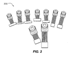
- FIG. 2 this figure illustrates several flex cables 200 any of which could comprise the data buses 110 and 120 inside a mobile phone or other electronic communications device according to one exemplary embodiment of the present invention.
- High-speed buses, such as 110 and 120 that generate EMI can take multiple forms, an example of which is a flex cable.
- a flex cable may also be referred to as a flex circuit, a flat cable, or a ribbon cable.
- a flex cable typically comprises a plurality of conductive traces or channels (typically copper conductors) embedded, laminated, or printed on or within a flexible molding structure such as a plastic or polymer film or some other dielectric or insulating material.
- the senor 115 , 125 comprises a conductive trace deposited on the flex cable 200 .
- the sensors 115 , 125 can be formed into or integrated with the flex cable 200 at the time that the flex cable 200 is manufactured, for example as a step in a manufacturing process that involves lithography.
- the flex cable 200 can alternatively be adapted following its manufacture, for example by adhering the sensor to the flex cable 200 . That is, a conventional flex cable can be acquired from a commercial vendor and processed to attach the sensor 115 , 125 to that cable.
- FIG. 3 this figure illustrates a functional block diagram of an interference compensation circuit 130 according to an exemplary embodiment of the present invention.
- the interference compensation circuit 130 shown in FIG. 3 can be embodied in a chip format as an integrated circuit (IC), as illustrated in FIG. 1 , or as a hybrid circuit.
- the interference compensation circuit 130 can comprise discrete components mounted on or attached to a circuit board or similar substrate.
- the system 100 that FIG. 1 illustrates can comprise the system 300 of FIG. 3 .
- the interference compensation circuit 130 draws or obtains power or energy from the power supply 360 , and its associated battery 365 . As will be discussed in further detail below, the interference compensation circuit 130 can operate in a plurality of modes, each having a different level of consumption of battery energy.
- FIG. 3 illustrates representative function blocks of the interference compensation circuit 130 , including a Variable Phase Adjuster 305 , a Variable Gain Amplifier (VGA) 310 , an emulation filter 315 , a Variable Delay Adjuster 320 , a Summation Node 325 , a power detector 330 , and a controller 335 .
- VGA Variable Gain Amplifier
- the interference sensor 115 obtains a sample of the aggressor signal by, for example, coupling to the interfering field.
- the sampled interfering signal is fed through the compensation circuit 130 starting with the Variable Phase Adjuster 305 .
- the phase adjuster may match, at the summation node 325 , the phase of the emulated compensation signal with the phase of the interfering signal coupled onto the victim antenna 340 . That is, the phase adjuster 305 places the phase of the compensation signal in phase with respect to the phase of the interference so that, when one is subtracted from the other, the compensation signal can cancel, or reduce, the interference.
- the cancellation can occur at the summation node 325 by subtracting the coupled signal onto the victim antenna 340 from the emulated signal generated by the interference compensation circuit 130 using the interfering signal as sampled at sensor 115 .
- the phase adjuster 305 can adjust the emulated signal phase to be 180 degrees out of phase with the interfering coupled signal. In that case, the summation node 325 adds the two signals rather than performing a subtraction.
- the phase shifter 305 comprises quadrature hybrids, and four silicon hyper-abrupt junction varactor diodes, along with various resistors, inductors and capacitors for biasing, pull-up, and signal conditioning.
- the phase shifter 305 comprises an active circuit.
- the optional emulation filter 315 can follow the variable phase shifter 305 in the cancellation path.
- the emulation filter 315 is typically a band pass (BP) filter that models the channel coupling and is also tunable in order to compensate for any drifts in channel center frequency.
- BP band pass
- the emulation filter 315 comprises lumped elements and varactor diodes.
- the varactor diodes help change or control the center frequency of the emulation channel.
- the emulation filter 315 is a Finite Impulse Response (FIR) filter.
- the FIR filter can comprise taps and tap spacings that are extracted from or determined according to the coupling channel characteristics.
- the emulation filter 325 typically should match, in general, the coupling channel characteristics within the frequency band of interest.
- the next stage of the cancellation path is the controllable delay adjuster 320 , which may provide a match between the group delay of the coupled signal through the victim antenna 340 and the group delay of the emulated compensation signal at the summation node 325 .
- the output of the delay adjuster 320 feeds into the VGA 310 .
- the VGA 310 can match the emulated signal amplitude to the amplitude of the interference signal at the summation node 325 .
- the emulation filter 315 models the frequency characteristics (i.e. attenuation of frequencies relative to other frequencies) of the coupling channel
- the VGA 310 applies a gain that is constant in magnitude across the frequency band of interest.
- the emulation filter 315 and the VGA 310 can function collaboratively to match the magnitude of the channel's coupling response on an absolute scale, rather than merely a relative scale.
- the VGA 310 feeds the interference compensation signal to the summation node 325 .
- the summation node 325 applies the compensation signal to the victim channel to negate, cancel, attenuate, or suppress the interference.
- the summation node 325 comprises a directional coupler.
- the summation node 325 comprises an active circuit such as a summer, which is typically a three-terminal device, or an output buffer, which is typically a two-terminal device.
- the summation node 325 should introduce essentially no mismatch to the victim antenna signal path. That is, the summation node 325 should ideally maintain characteristic impedance of the system 130 . Nevertheless, in some situations, small or controlled levels of impedance mismatch can be tolerated. Avoiding impedance mismatch implies that the summation node 325 should have a high output impedance at the tap. Additionally, the summation node 325 should not add significant loss to the victim antenna receive path, as such loss can adversely affect receiver sensitivity. For illustrative purposes, this discussion of impedance matching references a system with a characteristic impedance of 50-ohms; however, exemplary embodiments of the present invention can be applied to systems with essentially any characteristic impedance.
- FIG. 3 illustrates the components 305 , 310 , 315 , 320 is a particular order, that order is exemplary and should not be considered as limiting. Moreover, the order of those components 305 , 310 , 315 , 320 is usually not critical and can be changed, or the components 305 , 310 , 315 , 320 can be rearranged, while maintaining acceptable performance of the interference compensation circuit 130 .
- the interference compensation circuit 130 which can be viewed as an EMI canceller, offers flexibility in that the cancellation or compensation parameters can be adjusted or controlled to optimize the match of the emulated coupling channel to the actual EMI coupling channel. More specifically, the controller 335 and its associated power detector 330 provide a feedback loop for dynamically adjusting the circuit elements 305 , 310 , 315 , 320 in a manner that provides robust correction of interference. A discussion of exemplary embodiments of the interference compensation circuit 130 follows below with reference to FIGS. 8-20 .
- FIG. 4 this figure illustrates a frequency plot 410 of the spectral content of an interference signal prior to interference compensation overlaid upon a plot 420 of the spectral content of the interference signal following interference compensation according to an exemplary embodiment of the present invention. That is, the graph 400 illustrates laboratory test data collected before and after an application of interference compensation in accordance with an exemplary embodiment of the present invention.
- FIG. 4 shows the coupling channel characteristics between a flex cable, similar to the flex cables 200 illustrated in FIG. 2 and discussed above, and a 2.11 gigahertz (GHz) antenna.
- the test data shows that, in laboratory testing, an exemplary embodiment of an interference compensation circuit 130 achieved a signal reduction greater than 25 dB in the frequency band between 2.1 GHz and 2.15 GHz.
- FIGS. 5 and 6 respectively show spectral plots 500 , and 600 before and after applying interference compensation according to an exemplary embodiment of the present invention. More specifically, the traces 520 , and 620 of these plots 500 , and 600 illustrate data obtained in laboratory testing of an interference compensation system in accordance with an exemplary embodiment of the present invention.
- the spectra 520 , and 620 characterize a 450 megabits-per-second (“Mbps”) (PRBS-31) interfering signal coupled onto a 2.1 GHz antenna that is in close proximity to a flex cable carrying the 450 Mbps signal.
- Mbps megabits-per-second
- PRBS-311 450 megabits-per-second
- the compensation achieved approximately 12 dB of interference suppression.
- the interference compensation circuit 130 can function or operate in at least two modes. In one mode, the circuit 130 can consume less power than in the other mode. That is, the interference compensation circuit 130 can transition from an active mode of relatively high power usage to another mode of relatively low power usage.
- the lower power mode can be a standby mode, a power-saving mode, a passive mode, an idle mode, a sleep mode, or an off mode, to name a few possibilities.
- the interference compensation circuit can draw a reduced level of power, minimal power, essentially no power, or no power at all. Part or all of the interference compensation circuit illustrated in FIG. 3 and discussed above can be disconnected from power in the low power mode.
- An occurrence of one criterion or multiple criteria or conditions can trigger a transition from active compensation to a standby mode.
- the transition can occur automatically in response to an event other than a user turning off an appliance, such as a cell phone, that comprises the circuit 130 .
- operating the interference compensation circuit 130 in a power-saving mode can extend the operation time of a single battery charge, thereby enhancing the commercial attractiveness of the handset. Power reduction can be implemented or achieved without degrading interference compensation performance.
- Conditions occur in wireless handset devices that provide an opportunity for reduced power consumption.
- many of the EMI sources are not always active and, therefore, are not always emitting interference.
- the circuit 130 can transition to a sleep or stand-by mode of reduced power consumption. That is, rather than having one or more circuit elements receiving power while not producing an output or actively manipulating signals, power can be removed from those elements or from a selected set of circuit elements.
- the system 100 experiences states in which operating certain components of the interference compensation circuit 130 is unnecessary.
- the controller 335 can place those components in a low-power or standby mode or can remove power entirely from those components. For example, when an EMI source is not active for a threshold amount of time, the interference compensation circuit 130 can transition to the standby mode. More specifically, when the bus 110 is not actively carrying data traffic, the interference compensation circuit 130 can switch to the standby mode to conserve battery power.
- the sensor 115 provides a signal that is indicative of whether the bus 110 is active. That is, the level, voltage, amplitude, or intensity of the signal that the sensor 115 output can provide an indication of whether the bus is actively transmitting aggressor signals.
- electrical power can be removed from the components 305 , 310 , 315 , 320 that generate the emulated EMI signal. And, power can additionally or optionally be removed from some or all of the circuitry of the control module 335 .
- components used to store the emulation characteristics or parameters i.e. the emulation channel settings that match the coupling channel, can be kept active so as to immediately or quickly restore the interference compensation circuit's emulation channel to its last known state when the EMI source (e.g. the aggressor channel 110 ) is reactivated.
- the memory system of the controller 335 can retain power access to avoid loss of the parametric values stored in memory.
- the parametric values in memory facilitates rapid restoration to active cancellation upon reactivation of the EMI source.
- recalling the operational settings of the phase adjuster 305 , the emulation filter 315 , the delay adjuster 320 , and the VGA 310 avoids the interference that would occur if the emulation was retrained from an arbitrary reset state following transition from standby mode to active mode.
- Operating in the standby mode can comprise either full powering down one or more circuit components and/or operating in a state of reduced power usage. In some instances, the latter may be preferred in order to rapidly bring the component out of the standby state when the EMI source is reactivated.
- a standby signal instructs or triggers the interference compensation circuit 130 to transition to its power-saving or standby state.
- the standby signal can also trigger the transition from the power-saving or standby state to an active state.
- a device transmitting the source of the EMI, or an associated power detector can generate a signal indicating that it is actively transmitting data.
- the DSP chip 135 that sends data to the display 140 in the mobile phone system 100 can output an binary signal or code to indicate that it not transmitting data and consequently emitting EMI.
- the camera imaging sensor 145 that sends data to a the DSP chip 135 can output a binary signal or a digital code to indicate whether or not it is transmitting data that could produce EMI.
- a radio device that uses time-division multiplexing can provide the triggering standby signal. Such a radio device can be used in GSM or wideband code division multiple access (W-CDMA) applications, for example. In this situation, the radio may output a binary signal to mark the time divisions or intervals in which it is transmitting data. During those portions of the duplexing stage, the interference compensation should be active, as the transmitted signal can aggress a second radio device on a wireless handset.
- a power detector such as the detector 330 but attached to the output of the sampler 115 , examines the sampled EMI signal and generates the standby signal based on properties of the sampled EMI signal. For example, a standby state can be set if the detector 330 determines that power of the sampled EMI signal is below a given or predetermined threshold. Conversely, the interference compensation circuit 130 can be activated when the detected power moves above the threshold.
- the standby state can be declared if the time-localized peak amplitude of the sampled EMI signal falls below a given threshold.
- One advantage of this embodiment is that its implementation does not typically require an extra pin on the device package to be fed a dedicated standby signal. Instead, the standby signal could be derived from an available pin already used for EMI cancellation.
- a transition between standby and active mode can occur in response to a change in the strength of a reception signal.
- a circuit can become active when the number of reception “bars” on a cellular telephone reach a threshold level.
- a transition can occur in response to a change in a data rate or a bit rate, for example.
- all the components 305 , 310 , 315 , 320 of the emulation channel that are used to generate the emulated EMI signal from the sensor's sampled EMI source signal can be placed in the low-power standby state.
- one or more of the following components are placed in standby mode in response to an occurrence of a standby condition: the phase adjuster 305 , the BP channel emulation filter 315 , the delay adjuster 320 , and the VGA 310 . Reducing power consumption of those devices components 305 , 310 , 315 , 320 facilitates significant power savings when the EMI source is inactive.
- the controller 335 which can also be referred to as a control module, can be inactive when the EMI source is inactive. With no source of EMI and an inactive controller 335 , interference is not typically problematic. More specifically, no EMI occurs, and the emulation path is producing a zero emulation signal. In many circumstances, an improvement in interference performance can result from deactivating the emulation path when no source of EMI is active. If the emulation channel remains active when no EMI source is active, the emulation channel parameters may drift towards a set of values that poorly match the underlying EMI coupling channel. In this situation, activating the EMI source can result in poor tuning that causes the interference compensation circuit 130 to learn new, more effective parameters. In other words, when the interference compensation circuit 130 is inactive, an improperly tuned coupling channel can still produce a zero emulation signal since the sampled EMI source signal will be zero.
- all of the components, or essentially all of the active components, of the control module can be placed in the standby state when the standby signal is asserted, thereby providing a high level of power savings.
- the register or memory elements used to store the controllable parameters in the emulation channel are fully powered, while the rest of the control module 335 is deactivated.
- This embodiment facilitates rapidly or immediately returning the emulation channel to its pre-standby state when the system exits the standby mode.
- the interference compensation circuit 130 can resume cancellation from a previously-known and accurate channel model, rather than starting the cancellation from an arbitrary reset state. Resuming operation of the interference compensation circuit 130 from an arbitrary set of parameters may take an undesirably long period of time prior to convergence to an accurate channel model. During this learning time, EMI cancellation performance may be insufficient or inadequate.
- FIG. 7 this figure illustrates a flowchart of a process 700 for operating an interference compensation circuit 130 in a plurality of modes in accordance with an exemplary embodiment of the present invention.
- the Process 700 which is entitled Operate Interference Compensation Circuit, can be viewed as a process for managing power consumption of an interference compensation circuit 130 .
- a data transmitter such as the camera 145 or the DSP chip 135 issues a standby signal that can comprise a digital code.
- the code carries the status of the transmitter, for example whether the transmitter is actively transmitting data or is in a passive state between two time periods of data transmission. In one embodiment, the code specifies whether the transmitter is preparing to actively transmit data or to change between operational states.
- Step 710 the controller 335 receives the standby signal and determines whether the transmitter is in an active state of transmitting data or a passive state. Decision Step 715 branches the flow of Process 700 to Step 725 if the standby signal indicates that the transmitter is active. If, on the other hand, the standby signal indicates that the transmitter is passive, then decision Step 720 follows Step 715 .
- Step 720 the controller 335 determines whether the interference compensation circuit 130 is in an active mode or is otherwise in a passive mode. If the interference compensation circuit 130 is in an active mode, then Step 730 follows Step 720 .
- the controller 335 stores the current or present compensation parameters in memory and removes power from the emulation channel components 305 , 310 , 315 , 320 . This action places the interference compensation circuit 130 in a standby or power-saving mode.
- the stored compensation parameters typically comprise the settings of each of the adjustable components 305 , 310 , 315 , 320 of the emulation channel.
- Step 720 the controller 335 determines that the interference compensation circuit 130 is in the standby mode rather than the active mode, then Step 740 follows Step 720 .
- Step 740 the interference compensation circuit 130 remains in the standby mode.
- Step 715 branches the flow of Process 700 to Step 725 rather than Step 720 (based on the standby signal indicating active data transmission), then at decision Step 725 , the controller 335 determines whether the interference compensation circuit 130 is in active mode or standby mode.
- Step 745 follows Step 725 .
- the interference compensation circuit 130 remains in active mode.
- Step 735 determines at decision Step 725 that the interference compensation circuit 130 is in standby mode rather than active mode, then Step 735 follows Step 725 .
- the controller 335 recalls the current or last-used compensation parameters from memory and restores power to the powered-down components. Restoring power typically comprises initializing each of the adjustable components 305 , 310 , 315 , 320 of the emulation channel with the parametric settings recalled from memory.
- Step 750 follows execution of either of Steps 735 or 745 .
- the interference compensation circuit 130 generates an estimate of the interference based on processing the aggressor sample, which the sensor 115 obtained.
- the emulation channel components 305 , 310 , 315 , 320 process the sample to output the interference estimate.
- the interference compensation circuit 130 applies the interference estimate to the victim channel to cancel, suppress, or correct the interference occurring thereon.
- Process 700 loops back to and executes Step 705 as discussed above. Execution of Process 700 continues following the loop iteration.
- FIG. 8 this figure illustrates a functional block diagram of an EMI compensation circuit 130 A according to one exemplary embodiment of the present invention.
- the illustrated circuit 130 A can be an exemplary embodiment of the system 130 discussed above.
- a tap of the aggressor signal 850 is provided to the emulation channel 810 which acts upon the aggressor signal to mimic the aggressor signal that was coupled onto the victim signal.
- the aggressor signal may have suffered one or more of phase shift, amplitude loss, and frequency selective coupling, for example.
- the stages 315 , 310 , 305 within the emulation channel 810 represent these coupling effects.
- the stages 315 , 310 , 305 process the signal from the aggressor tap 850 to create a signal that matches the aggressor signal, as coupled into the victim signal.
- the emulation channel 810 comprises mechanisms such as the primary emulation filter 315 , a VGA 310 , and a variable phase adjuster 305 .
- the primary emulation filter 315 is a fixed filter that serves as a coarse-scale model of the coupling channel.
- the channel modeling is then refined by the variable gain 310 and phase adjust 305 stages to fine-tune the match to the actual coupling channel.
- the emulated coupling signal generated by the emulation channel 810 may then be subtracted from the corrupted victim signal at the summation node 325 .
- the generated emulated aggressor signal should substantially equal the actual aggressor signal, which is incurred by the received victim.
- the aggressor should be substantially removed from the victim signal.
- the phase control stage 335 A determines the amount of phase adjustment in the phase adjuster 305 by generating an analog control signal ⁇ ⁇ (alpha, sub phi). This control signal is fed into the phase adjuster 305 and directly determines the amount of phase adjustment applied in the emulation channel.
- the gain control stage 335 B sets the amount of gain adjustment in the VGA 310 by generating an analog control signal ⁇ g (alpha, sub g). This control signal is fed into the VGA 310 and directly specifies the amount of gain adjustment applied in the emulation channel.
- FIG. 9 this figure illustrates a functional block diagram of an exemplary embodiment of the phase control stage 335 A shown in FIG. 8 , discussed above.
- the phase control stage 335 A receives the emulated aggressor signal from the emulation channel 810 and samples corrupted victim signal.
- the phase control stage 335 A processes those received signals to produce a new value ⁇ ⁇ (alpha, sub phi) for the phase adjuster 305 .
- the emulated aggressor signal is split into a pair of emulated aggressor signals to which an additional phase adjustment or a temporal delay is applied.
- a phase of ⁇ ⁇ 1 (delta sub phi one) is added to the first signal of the split pair via the phase shifter (or delay) 910 A, thereby yielding an output signal that represents the emulation signal with total phase adjustment of ⁇ 0 + ⁇ ⁇ 1 .
- a phase of ⁇ ⁇ 2 (delta sub phi two) is added to the second of the split pair via phase shifter 910 B to yield an output signal that represents the emulation signal with a total phase adjustment of ⁇ 0 + ⁇ ⁇ 2 .
- the corrupted victim signal is also split into a first and second corrupted victim signal.
- Summation node 920 A subtracts the output of the first phase shifter 910 A from the first of the split pair of the corrupted victim signal to yield the aggressor-cancelled victim signal using a phase adjustment of ⁇ 0 + ⁇ ⁇ 1 .
- Summation node 920 b subtracts the output of the second phase shifter 910 b from the second of the split pair of the corrupted victim signal to yield the aggressor-cancelled victim signal using a phase adjustment of ⁇ 0 + ⁇ ⁇ 2 .
- the energy of each of the aggressor-cancelled victim signals is then obtained by application of a power-detecting device 930 A, 930 B followed by a low-pass filter (LPF) 940 A, 940 B to each of the signals.
- LPF low-pass filter
- the outputs of the LPFs 940 A and 940 B represent the energy of the aggressor-cancelled victim signals with extra phase adjustments of ⁇ ⁇ 1 and ⁇ ⁇ 2 (beyond the phase of ⁇ 0 applied in the emulation channel), respectively.
- the energy of the aggressor-cancelled victim signal may equal the sum of (i) the energy of the victim signal alone plus (ii) the energy of the cancelled aggressor component. This decomposition holds because the aggressor and victim signal are statistically independent signals. This energy-decomposition property is relevant because the subtraction device 950 , subtracts the pair of energy signals for the aggressor-cancelled victim signals.
- the energy contributions of the victim signal can nullify each other at the output of the subtraction node 950 .
- the output of the subtraction node 950 is the difference of the energies of the cancelled aggressor with an extra phase of ⁇ ⁇ 1 and the cancelled aggressor with an extra phase of ⁇ ⁇ 2 .
- the output of the subtraction node 950 is equivalent to the mathematical derivative of the residual aggressor energy with respect to phase. In particular, it approximates the negative derivative around the phase value ⁇ 0 +( ⁇ ⁇ 1 + ⁇ ⁇ 2 )/2.
- the system can converge to a state that results in the subtraction node 950 output being zero, or nearly zero. This state can correspond to the energy of the residual aggressor being minimized with respect to phase adjustment, and thus an optimum control value is achieved.
- FIG. 10 this figure illustrates a functional block diagram of an exemplary embodiment of the gain control stage 335 B illustrated in FIG. 8 , discussed above.
- the operation of this control stage is somewhat similar to that of the phase control stage 335 A.
- the gain control stage 335 B takes as inputs the emulated aggressor signal from the emulation channel 810 and the corrupted victim signal.
- the gain applied by the VGA 310 in the emulation channel 810 will be denoted as A 0 (A sub zero).
- the emulated aggressor signal is split into a pair of emulated aggressor signals to which an additional gain or attenuation is applied.
- An additional gain of 1+ ⁇ g is applied to the first signal of the split pair via the amplifier 1010 A to yield an output signal that represents the emulation signal with total gain of A 0 +A 0 ⁇ g .
- a gain of 1 ⁇ g is applied to the second of the split pair via amplifier 1010 B to yield an output signal that represents the emulation signal with a total gain of A 0 ⁇ A 0 ⁇ g .
- the effect of amplifier 1010 B may also be interpreted as attenuation since the gain factor 1 ⁇ g is typically less than one.
- the corrupted victim signal is also split into a first and second corrupted victim signal.
- Summation node 1020 A subtracts the output of the first amplifier 1010 A from the first of the split pair of the corrupted victim signal to yield the aggressor-cancelled victim signal using a gain of A 0 +A 0 ⁇ g .
- Summation node 1020 B subtracts the output of the second amplifier 1010 B from the second of the split pair of the corrupted victim signal to yield the aggressor-cancelled victim signal using a gain of A 0 ⁇ A 0 ⁇ g .
- the energy of each of the aggressor-cancelled victim signals is then obtained by application of a power-detecting device 1030 A, 1030 B followed by a low-pass filter (LPF) 1040 A, 1040 B to each of the signals.
- the outputs of the LPFs 1040 A and 1040 B represent the energy of the aggressor-cancelled victim signals with extra gains of 1+ ⁇ g and 1 ⁇ g (beyond the gain of A 0 applied in the emulation channel), respectively.
- the subtraction device 1050 subtracts the pair of energy signals for the aggressor-cancelled victim signals.
- the output of the subtraction node 1050 is the difference of the energies of the cancelled aggressor with an extra gain of 1+ ⁇ g and the cancelled aggressor with an extra gain of 1 ⁇ g .
- output of the subtraction node 1050 is equivalent to the mathematical derivative of the residual aggressor energy with respect to gain. In particular, it approximates the negative derivative around the gain value A 0 .
- the system can converge to a state which results in the subtraction node 1050 output being zero or nearly zero. This state corresponds to the energy of the residual aggressor being substantially minimized with respect to gain adjustment. Thus, a substantially optimum control value may be achieved.
- FIG. 11 this figure illustrates a functional block diagram of phase and gain control modules combined into a single control module 335 C for an EMI cancellation device 130 B according to one exemplary embodiment of the present invention.
- the system 130 B can be an exemplary embodiment of the system 130 of FIG. 3 , discussed above.
- phase control module 335 A and gain control module 335 B of those figures comprise certain duplicate circuit components.
- the otherwise redundant components provide both gain-control and phase-control functionality, thereby creating a more compact or efficient circuit.
- Benefits from reducing circuit redundancy can include lower power consumption, reduced parasitic effects, and smaller circuit size. That is, a beneficial circuit can be realized by integrating the phase and gain control modules into a single control module 335 C within the EMI cancellation device 130 B.
- the combined module 335 C takes a third input (beyond the corrupted received victim signal and emulated aggressor signal) to select the operational mode.
- the module 335 can be characterized as a controller that has two modes of operation, one for gain control and one for phase control.
- a mode-selector signal serves as a switch, controlling whether the module 335 C should adjust the gain or the phase of the emulation channel 810 at any given time.
- the control module 335 C outputs both the gain control signal ⁇ g and the phase control signal ⁇ ⁇ . In one mode, the control module 335 C makes gain adjustments while holding phase constant. In the other mode, the control module 335 C makes phase adjustments while holding gain constant. In an alternative embodiment, gain and phase may be concurrently adjusted.
- FIG. 12 discussed below, illustrates an exemplary embodiment of the combined control module 335 C.
- FIG. 12 the figure illustrates a functional block diagram for the combined gain and phase control module 335 C.
- the combined gain and phase control module 335 C has certain functional similarities to that of the phase control module 335 A and gain control module 335 B.
- One distinction is the five switches 1210 A- 1210 E of the gain control module 335 B that control whether gain or phase is being adjusted.
- switches 1210 A- 1210 E are set as shown in FIG. 12 . Specifically, switches 1210 A and 1210 C are set so that a first adjustment path adds gain beyond the nominal emulation channel 810 via amplifier 1010 A. Meanwhile, switches 1210 B and 1210 D are set so that a second adjustment path reduces gain after the nominal emulation channel 810 via amplifier 1010 B. And, switch 1210 E is set so that the derivative output is fed to the integrator 1060 for gain control. Under these settings, the control module 335 C operates in the same fashion as the gain control module 335 B described earlier.
- switches 1210 A- 1210 E all change to the opposite state of that shown in FIG. 12 .
- switches 1210 A and 1210 C are set so that the first adjustment path adds a first phase or equivalently a delay offset beyond the nominal emulation channel 810 via phase shifter 910 A.
- switches 1210 B and 1210 D are set so that a second adjustment path adds a second phase offset beyond the nominal emulation channel 810 via phase shifter 910 B.
- switch 1210 E is set so that the derivative output is fed to the integrator 960 for phase control. Under these settings, the control module 335 C operates in the same fashion as the phase control module 335 A described earlier.
- the mode selection input signal to the control module 335 C can be obtained in a variety of ways.
- a clock signal can be used as the model selection signal to periodically alternate between gain and phase adjustment according to a fixed interval.
- Another option is to use the derivative signal output from the summing node 950 .
- the mode selection signal can be toggled to change the mode of operation. This can be done on a continuing basis to constantly maintain substantially optimized gain and phase adjustments.
- control module 335 C can switch between operational modes in response to an occurrence of a time event, a signal event, or a condition or conditional event.
- the switch can occur automatically or based on a rule of operation, a signal change, feedback, a signal analysis result, a signal exceeding or meeting a predefined threshold, or an operational state.
- a mode change can occur on a recurring time basis or at a designated time or time interval.
- a transition between control modes can occur in response to a change in the strength of a reception signal.
- a mode change can automatically occur when the number of reception “bars” on a cellular telephone reach a threshold level.
- a transition can occur in response to a change in a data rate or a bit rate, for example.
- FIG. 13 this figure illustrates an interference compensation circuit 1300 that can be coupled to an interference sensor 115 , 125 according to an exemplary embodiment of the present invention.
- the system 100 illustrated in FIG. 1 and discussed above can comprise the circuit 1300 rather that the circuit 130 .
- This embodiment is composed of a high-impedance tap 1310 of the corrected victim signal 1305 after noise cancellation summer 1380 .
- the circuit 1300 comprises a power detector 1320 that can be an RMS detector or a peak power detector, for example.
- the power detector 1320 is followed by a switch 1330 that selects one of at least two sample-and-hold circuits 1340 A, 1340 B.
- the sample-and-hold circuits 1340 A, 1340 B feed a comparator or multiple comparators 1350 .
- the outputs of the comparator 1350 goes to the control and timing circuit 1360 .
- the control and timing circuit 1360 provides timing to the switch 1330 , sample-and-hold circuits 1340 , comparator(s) 1350 , and other control circuits as needed.
- the control and timing circuit 1360 also controls the emulation channel 810 of the active wireless canceller.
- the emulation channel 810 acts upon a tap or sample of the aggressor signal 850 to attempt to mimic the aggressor signal that was coupled onto the victim signal as discussed above.
- the interference compensation circuit 1300 can operate in two or more modes, one of which offers reduced power consumption relative to the other.
- the circuit 1300 transitions to a power-saving mode upon occurrence of a trigger event.
- power can be removed from one or more of the power detector 1320 , the switching device 1330 , the sample and hold circuits 1340 A and 1340 B, and the comparator 1350 .
- the power detector 1320 and comparator 1350 are two leading contributors to power consumption, thus disconnecting their power supply can achieve significant power savings.
- the control and timing circuit 1360 typically comprises low-speed digital logic that consumes negligible power. Nonetheless, most of this circuit 1360 can be deactivated with the exception of the registers, which store the values of the emulation channel 810 parameters.
- the Figure illustrates a logical flow diagram of a process for optimizing emulation channel parameters according to one exemplary embodiment of the present invention.
- the control and timing circuit performs a gradient optimization of the emulation channel parameters and coordinates the timing of all the control loop circuits.
- emulation filter parameters such as gain and phase
- Step 1410 emulation filter parameters, such as gain and phase, are perturbed by a small amount individually or simultaneously.
- Step 1420 the impact of the change on noise is assessed and in Step 1430 a decision is made regarding which direction to move.
- the process is then continuously repeated. Accordingly, the interference compensation parameters are adapted to address changes in operating environment, to thereby maintain an adequate level of interference compensation.
- FIG. 15 this figure illustrates a control and timing circuit 1360 according to one exemplary embodiment of the present invention.
- the results of the comparator(s) feed the decision state machine 1500 .
- the decision state machine then controls up/down counters 1520 , which control DACs 1530 .
- the DACs 1530 then control the gain, phase, and possibly other parameters of the emulation filter.
- a timing circuit 1510 coordinates the timing of the decision state machine with the other control loop circuits.
- the system 1360 of FIG. 15 is generally scalable to control a varying number of emulation channel parameters.
- the gain and phase of the emulation channel are exemplary parameters that can be controlled.
- Other parameters that might be controlled are delay and emulation filter parameters such as center frequency or pole-zero locations.
- FIG. 16 this figure illustrates an interference compensation circuit 1600 comprising a filter 1610 prior to the power detector 1320 .
- the filter 1610 before the power detector 1320 can be used to reject, or partially reject, the receive signal while substantially passing the aggressor signal such that the control loop is more sensitive to canceling the aggressor signal and can provide greater reduction of the aggressor signal below the receive signal.
- FIG. 16 also shows an exemplary embodiment that provides respective connections between multiple comparators 1350 and multiple sample-and-hold circuits 1340 .
- FIG. 17 this figure illustrates an interference compensation circuit 1700 comprising a down converter 1710 and IF filter 1720 prior to the power detector 1320 .
- the IF filter 1720 may have a response as shown in FIG. 18 where the down converted victim signal is rejected, but the residual aggressor noise is passed.
- a benefit of this illustrated embodiment of detecting the residual aggressor is that the fractional bandwidth of the rejected victim signal may be higher than the embodiment shown in FIG. 16 , thereby providing a simpler filter implementation.
- the overall result can provide a higher sensitivity to the aggressor residual over the victim signal in the control loop optimization.
- the control loop is usually not as sensitive to the residual aggressor. Higher reduction of the aggressor signal can be achieved when the victim signal response can be removed prior to the power detector in the control loop.
- FIG. 18 this figure illustrates frequency response 1800 of the IF filter 1720 , shown in FIG. 17 , according to one exemplary embodiment of the present invention.
- this figure illustrates an interference compensation circuit 1900 where the corrupted victim signal and the tapped aggressor signal 850 are both down converted by down converter 1910 and down converter 1930 , respectively, to an IF band prior to the cancellation summer 1380 .
- An advantage of this embodiment is that the emulation channel 810 and the control loop 1980 operate at the IF frequency instead of the RF frequency.
- the victim signal 1950 may not need further down conversion in the receiver.
- the filter 1720 before the control loop power detector 1320 has a higher fractional bandwidth for the victim signal, which makes rejection of the victim signal over the residual aggressor signal easier to implement with a realistic filter.
- the Figure illustrates an interference compensation circuit 2000 comprising a down converter 2010 already present in the radio.
- the tap-off 1310 is placed after down conversion to baseband frequencies and the addition of any extra mixing circuits (and associated power consumption) is avoided.
- a system in accordance with an exemplary embodiment of the present invention can comprise: a sensor that obtains a representative interference sample or a sample of an interfering signal; an emulation channel that processes the sampled interfering signal to generate an interference compensation signal; and a control loop for controlling the emulation channel.
- a system in accordance with an exemplary embodiment of the present invention can alternatively, or also, comprise a circuit that operates in two or more modes to cancel, correct, or compensate for interference imposed on one communication signal by another signal.
- the system can be applied to wireless communication devices, such as mobile phones, wireless base-stations, personal data assistants (PDAs), satellite or cable television components, computers, radar systems, wireless network elements, etc.
- PDAs personal data assistants
Landscapes
- Engineering & Computer Science (AREA)
- Computer Networks & Wireless Communication (AREA)
- Signal Processing (AREA)
- Noise Elimination (AREA)
Abstract
Description
Claims (11)
Priority Applications (2)
| Application Number | Priority Date | Filing Date | Title |
|---|---|---|---|
| US11/450,543 US7725079B2 (en) | 2004-12-14 | 2006-06-09 | Method and system for automatic control in an interference cancellation device |
| US12/757,362 US20100197233A1 (en) | 2004-12-14 | 2010-04-09 | Method and System for Automatic Control in an Interference Cancellation Device |
Applications Claiming Priority (7)
| Application Number | Priority Date | Filing Date | Title |
|---|---|---|---|
| US63581704P | 2004-12-14 | 2004-12-14 | |
| US68946705P | 2005-06-10 | 2005-06-10 | |
| US69690505P | 2005-07-06 | 2005-07-06 | |
| US71905505P | 2005-09-21 | 2005-09-21 | |
| US72032405P | 2005-09-23 | 2005-09-23 | |
| US11/302,896 US7522883B2 (en) | 2004-12-14 | 2005-12-14 | Method and system for reducing signal interference |
| US11/450,543 US7725079B2 (en) | 2004-12-14 | 2006-06-09 | Method and system for automatic control in an interference cancellation device |
Related Parent Applications (1)
| Application Number | Title | Priority Date | Filing Date |
|---|---|---|---|
| US11/302,896 Continuation-In-Part US7522883B2 (en) | 2004-12-14 | 2005-12-14 | Method and system for reducing signal interference |
Related Child Applications (1)
| Application Number | Title | Priority Date | Filing Date |
|---|---|---|---|
| US12/757,362 Division US20100197233A1 (en) | 2004-12-14 | 2010-04-09 | Method and System for Automatic Control in an Interference Cancellation Device |
Publications (2)
| Publication Number | Publication Date |
|---|---|
| US20070060059A1 US20070060059A1 (en) | 2007-03-15 |
| US7725079B2 true US7725079B2 (en) | 2010-05-25 |
Family
ID=46325588
Family Applications (1)
| Application Number | Title | Priority Date | Filing Date |
|---|---|---|---|
| US11/450,543 Expired - Fee Related US7725079B2 (en) | 2004-12-14 | 2006-06-09 | Method and system for automatic control in an interference cancellation device |
Country Status (1)
| Country | Link |
|---|---|
| US (1) | US7725079B2 (en) |
Cited By (9)
| Publication number | Priority date | Publication date | Assignee | Title |
|---|---|---|---|---|
| US20090029666A1 (en) * | 2007-07-24 | 2009-01-29 | Seiko Epson Corporation | Noise cancellation method, receiver circuit, and electronic instrument |
| US20120094610A1 (en) * | 2009-06-30 | 2012-04-19 | Nokia Corporation | Apparatus, Method, Computer Program for Communication and System Thereof |
| US20130103354A1 (en) * | 2011-10-25 | 2013-04-25 | International Business Machines Corporation | Detecting cross-talk on processor links |
| US8989672B2 (en) | 2011-01-07 | 2015-03-24 | Apple Inc. | Methods for adjusting radio-frequency circuitry to mitigate interference effects |
| US9087135B2 (en) | 2011-10-25 | 2015-07-21 | International Business Machines Corporation | Characterization and validation of processor links |
| US9094250B2 (en) | 2011-06-29 | 2015-07-28 | Telefonaktiebolaget L M Ericsson (Publ) | Method of channel cancellation, radio receiver, cellular communication device and computer program |
| US9113481B2 (en) | 2012-09-27 | 2015-08-18 | Qualcomm Incorporated | Adaptive non-linear interference cancellation using side-band information |
| US20150295607A1 (en) * | 2012-11-01 | 2015-10-15 | Zte Corporation | Intermediate-Frequency Analogue-to-Digital Conversion Device |
| US11047931B2 (en) | 2017-04-11 | 2021-06-29 | Apple Inc. | Magnetic field sensor array with electromagnetic interference cancellation |
Families Citing this family (37)
| Publication number | Priority date | Publication date | Assignee | Title |
|---|---|---|---|---|
| IL158211A0 (en) | 2001-04-04 | 2004-05-12 | Quellan Inc | Method and system for decoding multilevel signals |
| AU2003256569A1 (en) | 2002-07-15 | 2004-02-02 | Quellan, Inc. | Adaptive noise filtering and equalization |
| AU2003287628A1 (en) | 2002-11-12 | 2004-06-03 | Quellan, Inc. | High-speed analog-to-digital conversion with improved robustness to timing uncertainty |
| EP1594312A4 (en) * | 2003-02-13 | 2006-10-04 | Matsushita Electric Ind Co Ltd | SOLID STATE VIEWING DEVICE, ASSOCIATED CONTROL METHOD, AND CAMERA USING THE DEVICE |
| US8315583B2 (en) * | 2006-08-23 | 2012-11-20 | Quellan, Inc. | Pre-configuration and control of radio frequency noise cancellation |
| WO2005018134A2 (en) | 2003-08-07 | 2005-02-24 | Quellan, Inc. | Method and system for crosstalk cancellation |
| US7804760B2 (en) | 2003-08-07 | 2010-09-28 | Quellan, Inc. | Method and system for signal emulation |
| US7616700B2 (en) * | 2003-12-22 | 2009-11-10 | Quellan, Inc. | Method and system for slicing a communication signal |
| US7324167B2 (en) * | 2004-03-02 | 2008-01-29 | Magenta Research | High-quality twisted-pair transmission line system for high-resolution video |
| DE112007001045B4 (en) * | 2006-04-26 | 2019-05-16 | Intersil Americas LLC | Method and system for reducing radiation emissions from a communication channel |
| DE102007040712B4 (en) * | 2007-08-23 | 2014-09-04 | Seereal Technologies S.A. | Electronic display device and device for driving pixels of a display |
| CN102124659B (en) * | 2008-08-21 | 2014-02-26 | 英特赛尔美国股份有限公司 | Antenna module and method for noise cancellation using the antenna module |
| US20100074315A1 (en) * | 2008-09-24 | 2010-03-25 | Quellan, Inc. | Noise sampling detectors |
| US8036606B2 (en) * | 2009-02-03 | 2011-10-11 | Ubidyne, Inc. | Method and apparatus for interference cancellation |
| US8166084B2 (en) * | 2009-03-27 | 2012-04-24 | Intersil Americas Inc. | Calibration of adjustable filters |
| US8380771B2 (en) | 2009-03-27 | 2013-02-19 | Quellan, Inc. | Filter shaping using a signal cancellation function |
| US8422412B2 (en) | 2009-04-29 | 2013-04-16 | Quellan, Inc. | Duplexer and switch enhancement |
| US8429439B2 (en) * | 2009-05-20 | 2013-04-23 | Quellan, Inc. | Inter-pair skew adjustment |
| US8183711B2 (en) * | 2009-06-02 | 2012-05-22 | Quellan, Inc. | Power extraction from signal sinks |
| US9031592B2 (en) * | 2012-03-31 | 2015-05-12 | Tejas Networks Limited | Method and system for cancelling adjacent cells interference signal in a wireless communication system |
| US20150336463A1 (en) * | 2014-05-21 | 2015-11-26 | Delphi Technologies, Inc. | Active electromagnetic interference mitigation system and method |
| US9641205B1 (en) * | 2015-09-08 | 2017-05-02 | Amazon Technologies, Inc. | Active interference cancellation |
| US9924408B1 (en) * | 2016-08-24 | 2018-03-20 | Intel IP Corporation | Methods and devices for interference cancellation in cell search |
| US10581155B1 (en) * | 2018-09-27 | 2020-03-03 | Amazon Technologies, Inc. | Active interference cancellation |
| CN112769454B (en) * | 2019-10-21 | 2023-05-26 | 中兴通讯股份有限公司 | Interference cancellation device, simultaneous same-frequency full duplex system and wireless terminal |
| JP7261149B2 (en) * | 2019-12-04 | 2023-04-19 | 日立Astemo株式会社 | Electronic controller, control method, sensor system |
| EP4205288A4 (en) | 2020-08-28 | 2024-10-30 | ISCO International, LLC | METHOD AND SYSTEM FOR MITIGATING NEAR-FIELD INTERFERENCE |
| CN112836816B (en) * | 2021-02-04 | 2024-02-09 | 南京大学 | Training method suitable for crosstalk of photoelectric storage and calculation integrated processing unit |
| US11476574B1 (en) | 2022-03-31 | 2022-10-18 | Isco International, Llc | Method and system for driving polarization shifting to mitigate interference |
| US11990976B2 (en) | 2022-10-17 | 2024-05-21 | Isco International, Llc | Method and system for polarization adaptation to reduce propagation loss for a multiple-input-multiple-output (MIMO) antenna |
| US11949489B1 (en) | 2022-10-17 | 2024-04-02 | Isco International, Llc | Method and system for improving multiple-input-multiple-output (MIMO) beam isolation via alternating polarization |
| US11985692B2 (en) | 2022-10-17 | 2024-05-14 | Isco International, Llc | Method and system for antenna integrated radio (AIR) downlink and uplink beam polarization adaptation |
| US11956058B1 (en) | 2022-10-17 | 2024-04-09 | Isco International, Llc | Method and system for mobile device signal to interference plus noise ratio (SINR) improvement via polarization adjusting/optimization |
| US12348285B1 (en) | 2023-12-29 | 2025-07-01 | Isco International, Llc | Methods and systems for detecting, measuring, and/or locating passive intermodulation (PIM) sources via beamforming |
| US12301315B1 (en) | 2023-12-29 | 2025-05-13 | Isco International, Llc | Methods and systems for detecting, measuring, and/or locating passive intermodulation sources via downlink (DL) signal injection |
| US12301298B1 (en) | 2023-12-29 | 2025-05-13 | Isco International, Llc | Methods and systems for locating interference sources via angle of arrival (AoA) |
| US12219522B1 (en) | 2023-12-29 | 2025-02-04 | Isco International, Llc | Methods and systems for estimating the shape of an object generating passive intermodulation (PIM) interference |
Citations (290)
| Publication number | Priority date | Publication date | Assignee | Title |
|---|---|---|---|---|
| US2632058A (en) | 1946-03-22 | 1953-03-17 | Bell Telephone Labor Inc | Pulse code communication |
| US3445771A (en) | 1966-02-28 | 1969-05-20 | Honeywell Inc | Automatic data channel equalization apparatus utilizing a transversal filter |
| US3571725A (en) | 1967-05-25 | 1971-03-23 | Nippon Electric Co | Multilevel signal transmission system |
| US3599122A (en) | 1968-10-10 | 1971-08-10 | Philips Corp | Filter network including at least one tapped electromagnetic delay line |
| US3633108A (en) | 1969-03-18 | 1972-01-04 | Bell Telephone Labor Inc | Timing recovery through distortion monitoring in data transmission systems |
| US3714437A (en) | 1970-08-14 | 1973-01-30 | Bell Telephone Labor Inc | Optical communication system with pcm encoding with plural discrete unequally spaced intensity levels |
| US3806915A (en) | 1972-09-05 | 1974-04-23 | Us Navy | Multithreshold analog to digital converter |
| US3977795A (en) | 1973-02-15 | 1976-08-31 | Afga-Gevaert, A.G. | Method of determining the modulation transfer function |
| US4201909A (en) | 1977-10-13 | 1980-05-06 | Cselt - Centro Studi E Laboratori Telecomunicazioni S.P.A. | Data-transmission system and method using fiber-optical transmission |
| US4287756A (en) | 1979-10-24 | 1981-09-08 | Gallagher John J | Stratified fluid interface recorder |
| US4288872A (en) | 1979-05-11 | 1981-09-08 | Cselt - Centro Studi E Laboratori Telecomunicazioni S.P.A. | Equalizer for the correction of digital signals |
| US4349914A (en) | 1980-04-01 | 1982-09-14 | Ford Aerospace & Communications Corp. | Bit synchronous switching system for space diversity operation |
| US4363127A (en) | 1981-01-12 | 1982-12-07 | Ford Aerospace & Communications Corporation | Line signaling apparatus and techniques for digital data links |
| US4386339A (en) | 1980-03-31 | 1983-05-31 | Hewlett-Packard Company | Direct flash analog-to-digital converter and method |
| US4387461A (en) | 1981-03-11 | 1983-06-07 | Ford Aerospace & Communications Corporation | Experientially determined signal quality measurement device for antipodal data |
| US4393499A (en) | 1981-03-11 | 1983-07-12 | Ford Aerospace & Communications Corporation | Adaptive signal quality measurement circuit for PSK and FSK demodulators |
| US4410878A (en) | 1979-11-03 | 1983-10-18 | Licentia Patent-Verwaltungs-G.M.B.H. | Digital signal transmission |
| US4464771A (en) | 1982-04-02 | 1984-08-07 | Motorola, Inc. | Phase-locked loop circuit arrangement |
| US4470126A (en) | 1981-10-29 | 1984-09-04 | American Microsystems, Inc. | Programmable transversal filter |
| US4475227A (en) | 1982-04-14 | 1984-10-02 | At&T Bell Laboratories | Adaptive prediction |
| US4479266A (en) | 1981-08-12 | 1984-10-23 | Thomson-Csf | Multiple-threshold optical receiver for a variable-rate digital data transmission system |
| US4521883A (en) | 1981-06-22 | 1985-06-04 | Bernard Roche | Telephony apparatus having filter capacitor switched to undergo discrete phase jumps |
| US4580263A (en) | 1982-10-21 | 1986-04-01 | Mitsubishi Denki Kabushiki Kaisha | Signal quality monitoring device |
| US4584720A (en) | 1982-09-02 | 1986-04-22 | British Telecommunications | Optical communication system using pulse position modulation |
| US4618941A (en) | 1983-09-19 | 1986-10-21 | Motorola, Inc. | Apparatus and method for generating filtered multilevel data from NRZ data |
| US4646173A (en) | 1984-06-20 | 1987-02-24 | Robert Bosch Gmbh | Converting and decoding receiver for digital data recorded in analog form on magnetic tape |
| US4651026A (en) | 1983-07-06 | 1987-03-17 | Motorola, Inc. | Clock recovery circuit |
| US4688245A (en) * | 1983-12-01 | 1987-08-18 | Siemens Aktiengesellschaft | Method and circuit arrangement for compensating cross-talk and/or echo signals |
| US4751497A (en) | 1985-04-24 | 1988-06-14 | Iwatsu Electric Co., Ltd. | Digital to analog converter with high output compliance |
| US4830493A (en) | 1987-10-29 | 1989-05-16 | Beckman Instruments, Inc. | UV scanning system for centrifuge |
| US4847521A (en) | 1986-12-23 | 1989-07-11 | Thomson-Csf | Device for the amplification of light-sensitive |
| US4864590A (en) | 1987-12-31 | 1989-09-05 | Northern Telecom Limited | Apparatus and method for noise reduction in a digital line receiver |
| US4873700A (en) | 1987-10-14 | 1989-10-10 | National Semiconductor Corporation | Auto-threshold/adaptive equalizer |
| US4912726A (en) | 1987-01-12 | 1990-03-27 | Fujitsu Limited | Decision timing control circuit |
| GB2223369A (en) | 1988-08-18 | 1990-04-04 | Plessey Co Plc | Analogue-to-digital converters |
| US4942593A (en) | 1989-03-16 | 1990-07-17 | Dallas Semiconductor Corporation | Telecommunications interface with improved jitter reporting |
| US4953041A (en) | 1989-01-24 | 1990-08-28 | Maxtor Corporation | Read channel detector for use in digital magnetic recording systems |
| US4959535A (en) | 1987-06-11 | 1990-09-25 | British Telecommunication | Optical receiver circuit including a filter network to minimize noise |
| US4978957A (en) | 1989-03-10 | 1990-12-18 | Hitachi, Ltd. | High-speed analog-to-digital converter |
| US5007106A (en) | 1989-11-08 | 1991-04-09 | At&T Bell Laboratories | Optical Homodyne Receiver |
| US5008957A (en) | 1988-03-03 | 1991-04-16 | Nec Corporation | Multilevel optical signal transmitter |
| US5012475A (en) | 1990-04-17 | 1991-04-30 | Wavelength Lasers, Inc. | Analog compensation system for linear lasers |
| US5067126A (en) | 1989-05-30 | 1991-11-19 | Telecommunications Research Laboratories | Method and apparatus for mapping a digital signal carrier to another |
| US5072221A (en) | 1988-08-04 | 1991-12-10 | Signal Processing Technologies, Inc. | Error limiting analog to digital converter |
| US5111065A (en) | 1990-03-23 | 1992-05-05 | Massachusetts Institute Of Technology | Diode driver circuit utilizing discrete-value DC current source |
| US5113278A (en) | 1989-04-26 | 1992-05-12 | Canon Kabushiki Kaisha | Communication system and apparatus using chip signals |
| US5115450A (en) | 1989-07-06 | 1992-05-19 | Advanced Micro Devices, Inc. | High speed digital to analog to digital communication system |
| US5121411A (en) | 1990-07-24 | 1992-06-09 | Motorola, Inc. | Multi-edge clock recovery method |
| US5128790A (en) | 1989-04-25 | 1992-07-07 | Alcatel N.V. | Optical cable television transmission system |
| US5132639A (en) | 1989-09-07 | 1992-07-21 | Ortel Corporation | Predistorter for linearization of electronic and optical signals |
| US5151698A (en) | 1989-09-19 | 1992-09-29 | French State Represented By The Minister Of Post, Telecommunications And Space (Centre National D'etudes Des Telecommunications) | Method for the coding of a digital signal, coder and decoder to implement this method, regeneration method and corresponding regenerator utilizing pulse position modulation |
| US5181136A (en) | 1989-09-22 | 1993-01-19 | The University Of Ottawa | Optical homodyne DPSK receiver with optical amplifier |
| US5181034A (en) | 1991-04-30 | 1993-01-19 | Kabushiki Kaisha Toshiba | Digital to analog converter |
| US5184131A (en) | 1989-07-06 | 1993-02-02 | Nissan Motor Co., Ltd. | A-d converter suitable for fuzzy controller |
| US5208833A (en) | 1991-04-08 | 1993-05-04 | Motorola, Inc. | Multi-level symbol synchronizer |
| US5222103A (en) | 1991-01-02 | 1993-06-22 | Gte Laboratories Incorporated | Differential quadrature phase shift keying encoder for subcarrier systems |
| US5223834A (en) | 1991-11-29 | 1993-06-29 | Industrial Technology Research Institute | Timing control for precharged circuit |
| US5225798A (en) | 1989-02-13 | 1993-07-06 | Electronic Decisions Incorporated | Programmable transversal filter |
| US5237590A (en) | 1989-03-13 | 1993-08-17 | Hitachi, Ltd. | Timing extraction circuit and communication system utilizing the same |
| US5243613A (en) | 1991-11-05 | 1993-09-07 | Synchronous Communications, Inc. | Method and apparatus to compensate for distortion in optical transmission systems |
| US5252930A (en) | 1989-09-07 | 1993-10-12 | Ortel Corporation | Predistorter for linearization of electronic and optical signals |
| US5282072A (en) | 1991-11-19 | 1994-01-25 | Harmonic Lightwaves, Inc. | Shunt-expansive predistortion linearizers for optical analog transmitters |
| US5283679A (en) | 1990-12-15 | 1994-02-01 | Alcatel N.V. | Communications process, transmitter and receiver for analog signals |
| US5291031A (en) | 1992-04-06 | 1994-03-01 | Telecommunications Research Laboratories | Optical phase difference range determination in liquid level sensor |
| US5293406A (en) | 1991-03-11 | 1994-03-08 | Nippon Telegraph And Telephone Corporation | Quadrature amplitude modulator with distortion compensation |
| US5300930A (en) | 1990-11-02 | 1994-04-05 | France Telecom | Binary encoding method with substantially uniform rate of changing of the binary elements and corresponding method of incrementation and decrementation |
| US5321543A (en) | 1992-10-20 | 1994-06-14 | General Instrument Corporation | Apparatus and method for linearizing an external optical modulator |
| US5321710A (en) | 1993-04-19 | 1994-06-14 | Raynet Corporation | Predistortion method and apparatus for laser linearization |
| US5327279A (en) | 1992-07-17 | 1994-07-05 | United Technologies Corporation | Apparatus for linearization of optic modulators using a feed-forward predistortion circuit |
| US5343322A (en) | 1991-12-31 | 1994-08-30 | France Telecom | System of very-long-distance digital transmission by optical fiber with compensation for distortions at reception |
| EP0527966B1 (en) | 1990-05-11 | 1994-09-21 | Fondazione Ugo Bordoni | A multilevel coherent optical system |
| US5351148A (en) | 1993-01-25 | 1994-09-27 | Matsushita Electric Industrial Co., Ltd. | Optical transmission system |
| US5355240A (en) | 1991-09-06 | 1994-10-11 | Alcatel Cit | Optical communication link with correction of non-linear effects and optical signal processing method |
| US5361156A (en) | 1991-12-09 | 1994-11-01 | Scientific-Atlanta, Inc. | Method and apparatus for predistortion |
| US5371625A (en) | 1992-02-01 | 1994-12-06 | Alcatel N.V. | System for optically transmitting digital communications over an optical fiber with dispersion at the operating wavelength |
| US5373384A (en) | 1992-08-14 | 1994-12-13 | Alcatel Cit | Semiconductor light source with non-linear compensation means within a predistortion circuit |
| US5376786A (en) | 1992-06-23 | 1994-12-27 | Telecommunications Research Laboratories | Optoelectronic transversal filter with variable gain bi-polar taps |
| US5382955A (en) | 1993-11-04 | 1995-01-17 | Tektronix, Inc. | Error tolerant thermometer-to-binary encoder |
| US5387887A (en) | 1988-05-20 | 1995-02-07 | Texas Instruments Incorporated | Miniature digitally controlled programmable transversal filter using LSI GaAs integrated circuits |
| US5408485A (en) | 1994-05-11 | 1995-04-18 | Alcatel Network Systems, Inc. | Laser modulation controller using NRZ electrical modulation level control |
| US5413047A (en) | 1993-10-15 | 1995-05-09 | Atlantic Richfield Company | Overburden removal method with blast casting and excavating apparatus |
| US5418637A (en) | 1992-10-21 | 1995-05-23 | At&T Corp. | Cascaded distortion compensation for analog optical systems |
| US5424680A (en) | 1993-11-30 | 1995-06-13 | Harmonic Lightwaves, Inc. | Predistorter for high frequency optical communications devices |
| US5428831A (en) | 1993-01-08 | 1995-06-27 | American Nucleonics Corporation | Signal path length correlator and method and an interference cancellation system using the same |
| US5428643A (en) | 1992-08-25 | 1995-06-27 | U.S. Philips Corporation | Method of, and transmitter for, transmitting a digital signal |
| US5436756A (en) | 1992-09-30 | 1995-07-25 | At&T Bell Laboratories | Suppressed photocurrent, quantum well optical modulation device |
| US5436752A (en) | 1992-10-29 | 1995-07-25 | Alcatel N.V. | Receive-side circuit for a system for optically transmitting a digital signal over a dispersive optical waveguide |
| US5444864A (en) | 1992-12-22 | 1995-08-22 | E-Systems, Inc. | Method and apparatus for cancelling in-band energy leakage from transmitter to receiver |
| US5450044A (en) | 1993-04-14 | 1995-09-12 | Acrodyne Industries, Inc. | Quadrature amplitude modulator including a digital amplitude modulator as a component thereof |
| US5481568A (en) | 1992-02-14 | 1996-01-02 | Sony Corporation | Data detecting apparatus using an over sampling and an interpolation means |
| US5481389A (en) | 1992-10-09 | 1996-01-02 | Scientific-Atlanta, Inc. | Postdistortion circuit for reducing distortion in an optical communications system |
| US5483552A (en) | 1992-10-27 | 1996-01-09 | Matsushita Electric Industrial Co., Ltd. | Adaptive equalizing apparatus for controlling the input signal level of quantized feedback |
| US5504633A (en) | 1992-08-06 | 1996-04-02 | U.S. Philips Corporation | Apparatus, having a variable equalizer, for reproducing a digital signal from a record carrier |
| US5510919A (en) | 1993-12-04 | 1996-04-23 | Alcatel N.V. | Optical system for transmitting a multilevel signal |
| US5515196A (en) | 1992-04-07 | 1996-05-07 | Hitachi, Ltd. | Optical intensity and phase modulators in an optical transmitter apparatus |
| US5528710A (en) | 1992-05-05 | 1996-06-18 | British Telecommunications Public Limited Corporation | Optical switching device with passive input and output stages and active amplifier in a matrix stage |
| US5541955A (en) | 1992-11-06 | 1996-07-30 | Pericle Communications Company | Adaptive data rate modem |
| US5548253A (en) | 1995-04-17 | 1996-08-20 | Omnipoint Corporation | Spectrally efficient quadrature amplitude modulator |
| US5557439A (en) | 1995-07-25 | 1996-09-17 | Ciena Corporation | Expandable wavelength division multiplexed optical communications systems |
| US5574978A (en) * | 1994-05-12 | 1996-11-12 | American Nucleonics Corporation | Interference cancellation system and radio system for multiple radios on a small platform |
| US5574743A (en) | 1994-03-22 | 1996-11-12 | U.S. Philips Corporation | Semiconductor diode laser having improved performance and method of manufacturing same |
| US5589786A (en) | 1994-06-06 | 1996-12-31 | Cselt- Centro Studi E Laboratori Telecommunicazioni S.P.A. | High-speed CMOS driver for optical sources |
| US5604724A (en) | 1994-09-26 | 1997-02-18 | Nec Corporation | Maximum likelihood estimation using reference and spontaneous output peaks of partial response equalizer |
| US5606734A (en) | 1993-03-02 | 1997-02-25 | American Nucleonics Corporation | Structure generated composite reference signal for interference suppression in an adaptive loop |
| US5612653A (en) | 1995-06-07 | 1997-03-18 | Telecommunications Research Laboratories | LAN star connection using negative impedance for matching |
| US5617135A (en) | 1993-09-06 | 1997-04-01 | Hitachi, Ltd. | Multi-point visual communication system |
| US5621764A (en) | 1994-06-21 | 1997-04-15 | Nec Corporation | Soft decision signal outputting receiver |
| GB2306066A (en) | 1995-10-02 | 1997-04-23 | Northern Telecom Ltd | Clock recovery |
| US5625722A (en) | 1994-12-21 | 1997-04-29 | Lucent Technologies Inc. | Method and apparatus for generating data encoded pulses in return-to-zero format |
| US5625360A (en) | 1995-09-05 | 1997-04-29 | Motorola, Inc. | Current source for reducing noise glitches generated in a digital to analog converter and method therefor |
| US5644325A (en) | 1994-12-12 | 1997-07-01 | Auravision Corporation | Digital to analog converter with improved output level control |
| US5648987A (en) | 1994-03-24 | 1997-07-15 | Samsung Electronics Co., Ltd. | Rapid-update adaptive channel-equalization filtering for digital radio receivers, such as HDTV receivers |
| US5670871A (en) | 1994-04-28 | 1997-09-23 | Hoechst Celanese Corp | Polymeric film electrooptic sensor device |
| US5675600A (en) | 1995-09-27 | 1997-10-07 | Fujitsu Limited | Laser diode driver system |
| US5678198A (en) | 1991-05-22 | 1997-10-14 | Southwestern Bell Technology Resources, Inc. | System for controlling signal level at both ends of a transmission link, based upon a detected value |
| US5689356A (en) | 1995-02-02 | 1997-11-18 | Lucent Technologies Inc. | System and method for minimizing nonlinear distortion in optical communication systems employing laser intensity modulation |
| US5692011A (en) | 1994-06-15 | 1997-11-25 | International Business Machines Corporation | Dual decision equalization apparatus |
| US5691978A (en) | 1995-04-07 | 1997-11-25 | Signal Science, Inc. | Self-cancelling full-duplex RF communication system |
| US5699022A (en) | 1996-02-09 | 1997-12-16 | Dsc Communications Corporation | Adaptive cable equalizer |
| US5706008A (en) | 1996-03-01 | 1998-01-06 | Analog Devices, Inc. | High bandwidth parallel analog-to-digital converter |
| US5721315A (en) | 1993-07-13 | 1998-02-24 | Huntsman Petrochemical Corporation | Polyether amine modification of polypropylene |
| US5723176A (en) | 1994-03-02 | 1998-03-03 | Telecommunications Research Laboratories | Method and apparatus for making optical components by direct dispensing of curable liquid |
| US5751726A (en) | 1994-12-31 | 1998-05-12 | Hyundai Electronics Industries, Co. Ltd. | Representative value selector and an embodying method therefor |
| US5754681A (en) | 1994-10-05 | 1998-05-19 | Atr Interpreting Telecommunications Research Laboratories | Signal pattern recognition apparatus comprising parameter training controller for training feature conversion parameters and discriminant functions |
| US5757763A (en) | 1994-07-12 | 1998-05-26 | Massachusetts Institute Of Technology | Optical information storage via amplitude modulation |
| US5761243A (en) | 1993-09-16 | 1998-06-02 | U.S. Philips Corporation | Digital receiver with noise filter which also serves as a feedback filter providing intersymbol interference reduction |
| US5764542A (en) | 1996-01-11 | 1998-06-09 | Eaton Corporation | Noise filtering utilizing running average |
| US5774505A (en) | 1996-04-04 | 1998-06-30 | Hewlett-Packard Company | Intersymbol interference cancellation with reduced complexity |
| US5784032A (en) | 1995-11-01 | 1998-07-21 | Telecommunications Research Laboratories | Compact diversity antenna with weak back near fields |
| US5783630A (en) | 1993-07-13 | 1998-07-21 | Huntsman Petrochemical Corporation | Polyether amine modification of polypropylene |
| US5790595A (en) | 1994-09-02 | 1998-08-04 | Robert Bosch Gmbh | Method for obtaining bit-specific reliability information |
| US5798854A (en) | 1994-05-19 | 1998-08-25 | Ortel Corporation | In-line predistorter for linearization of electronic and optical signals |
| US5802089A (en) | 1996-10-22 | 1998-09-01 | Maxim Integrated Products, Inc. | Laser diode driver having automatic power control with smooth enable function |
| US5801657A (en) | 1997-02-05 | 1998-09-01 | Stanford University | Serial analog-to-digital converter using successive comparisons |
| US5812578A (en) | 1994-06-02 | 1998-09-22 | U.S. Philips Corporation | Radiation-emitting index-guided semiconductor diode |
| US5825825A (en) | 1996-09-17 | 1998-10-20 | Northern Telecom Limited | Method of processing multi-level signals for simple clock recovery |
| US5825211A (en) | 1995-09-29 | 1998-10-20 | Dallas Semiconductor Corporation | Oversampled state machine for jitter tolerant pulse detection |
| US5825257A (en) | 1997-06-17 | 1998-10-20 | Telecommunications Research Laboratories | GMSK modulator formed of PLL to which continuous phase modulated signal is applied |
| US5828329A (en) | 1996-12-05 | 1998-10-27 | 3Com Corporation | Adjustable temperature coefficient current reference |
| US5835848A (en) | 1996-12-30 | 1998-11-10 | Lucent Technologies Inc. | Range repeater for a transmission system |
| US5839105A (en) | 1995-11-30 | 1998-11-17 | Atr Interpreting Telecommunications Research Laboratories | Speaker-independent model generation apparatus and speech recognition apparatus each equipped with means for splitting state having maximum increase in likelihood |
| US5841841A (en) | 1995-03-16 | 1998-11-24 | Telecommunications Research Laboratories | Networking computers via shared use of voice telephone lines |
| US5844436A (en) | 1996-11-06 | 1998-12-01 | Northern Telecom Ltd. | Method of recovering a sampling clock in a framed data communications format with reduced phase jitter and wander |
| US5848139A (en) | 1996-11-19 | 1998-12-08 | Telecommunications Research Laboratories | Telecommunication traffic pricing control system |
| US5850409A (en) | 1997-03-21 | 1998-12-15 | Maxim Integrated Products, Inc. | Laser modulation control method and apparatus |
| US5850505A (en) | 1995-10-31 | 1998-12-15 | Telecommunications Research Laboratories | Method for preconfiguring a network to withstand anticipated failures |
| US5852389A (en) | 1997-04-11 | 1998-12-22 | Telecommunications Research Laboratories | Direct QAM modulator |
| US5859862A (en) | 1994-06-28 | 1999-01-12 | Hitachi, Ltd. | Optical recording/reproducing apparatus having laser diode driver capable of a linear operation responsive to an input signal representative of a laser beam power varying depending on a magneto-optical disk-laser beam spot relative speed |
| US5861966A (en) | 1995-12-27 | 1999-01-19 | Nynex Science & Technology, Inc. | Broad band optical fiber telecommunications network |
| US5872468A (en) | 1997-06-12 | 1999-02-16 | Northern Telecom Limited | Level detector circuit, interface and method for interpreting and processing multi-level signals |
| US5878390A (en) | 1996-12-20 | 1999-03-02 | Atr Interpreting Telecommunications Research Laboratories | Speech recognition apparatus equipped with means for removing erroneous candidate of speech recognition |
| US5880870A (en) | 1996-10-21 | 1999-03-09 | Telecommunications Research Laboratories | Optical modulation system |
| US5883910A (en) | 1997-07-03 | 1999-03-16 | Maxim Integrated Products, Inc. | High speed semiconductor laser driver circuits |
| US5887022A (en) | 1996-06-12 | 1999-03-23 | Telecommunications Research Laboratories | Peer-peer frequency hopping spread spectrum wireless system |
| US5889759A (en) | 1996-08-12 | 1999-03-30 | Telecommunications Research Laboratories | OFDM timing and frequency recovery system |
| US5896392A (en) | 1996-06-20 | 1999-04-20 | Nec Corporation | Device and method for automatically controlling decision points |
| US5912749A (en) | 1997-02-11 | 1999-06-15 | Lucent Technologies Inc. | Call admission control in cellular networks |
| US5920600A (en) | 1995-09-18 | 1999-07-06 | Oki Electric Industry Co., Ltd. | Bit phase synchronizing circuitry for controlling phase and frequency, and PLL circuit therefor |
| US5923226A (en) | 1996-08-13 | 1999-07-13 | Nec Corporation | Automatic equalizer |
| US5943380A (en) | 1996-03-29 | 1999-08-24 | Alcatel Telspace | Robust phase estimator and recoverer for digital signals affected in particular by phase jitter |
| US5943457A (en) | 1998-03-24 | 1999-08-24 | Telecommunications Research Laboratories | Generalized resonant coupler filters |
| US5949926A (en) | 1997-12-15 | 1999-09-07 | Telecommunications Research Laboratories | Minimum phase dispersion compensator |
| WO1999045683A1 (en) | 1998-03-05 | 1999-09-10 | Kestrel Solutions, Inc. | System and method for spectrally efficient transmission of digital data over optical fiber |
| US5959750A (en) | 1996-06-06 | 1999-09-28 | Lucent Technologies Inc. | Method of upgrading transmission capacity by Raman amplification |
| US5959032A (en) | 1993-07-13 | 1999-09-28 | Huntsman Petrochemical Corporation | Polyether amine modification of polypropylene |
| US5968198A (en) | 1996-08-16 | 1999-10-19 | Ericsson, Inc. | Decoder utilizing soft information output to minimize error rates |
| US5978417A (en) | 1996-02-23 | 1999-11-02 | National Semiconductor Corporation | Adaptive cable equalizer |
| US5983178A (en) | 1997-12-10 | 1999-11-09 | Atr Interpreting Telecommunications Research Laboratories | Speaker clustering apparatus based on feature quantities of vocal-tract configuration and speech recognition apparatus therewith |
| US5985999A (en) | 1993-07-13 | 1999-11-16 | Huntsman, Petrochemical Corporation | Dyeable polyolefin containing polyetheramine modified functionalized polyolefin |
| US5995565A (en) | 1995-10-10 | 1999-11-30 | Nortel Networks Corp | Co-channel interference reduction |
| US5999300A (en) | 1997-02-14 | 1999-12-07 | Telecommunications Research Laboratories | Hybrid single sideband optical modulator |
| US6002717A (en) | 1997-03-06 | 1999-12-14 | National Semiconductor Corporation | Method and apparatus for adaptive equalization using feedback indicative of undercompensation |
| US6009424A (en) | 1996-09-04 | 1999-12-28 | Atr Interpreting Telecommunications Research Laboratories | Similarity search apparatus for searching unit string based on similarity |
| US6011952A (en) | 1998-01-20 | 2000-01-04 | Viasat, Inc. | Self-interference cancellation for relayed communication networks |
| US6028658A (en) | 1996-04-18 | 2000-02-22 | Fuji Photo Film Co., Ltd. | Film viewer |
| US6031866A (en) | 1997-05-29 | 2000-02-29 | Telecommunications Research Laboratories | Duplex decision feedback equalization system |
| US6031048A (en) | 1993-07-13 | 2000-02-29 | Huntsman Petrochemical Corporation | Polyether amine modification of polypropylene |
| US6031874A (en) | 1997-09-26 | 2000-02-29 | Ericsson Inc. | Unequal error protection in coded modulation schemes |
| US6035080A (en) | 1997-06-20 | 2000-03-07 | Henry; Charles Howard | Reconfigurable add-drop multiplexer for optical communications systems |
| US6034996A (en) | 1997-06-19 | 2000-03-07 | Globespan, Inc. | System and method for concatenating reed-solomon and trellis codes |
| EP0584865B1 (en) | 1992-08-21 | 2000-03-15 | Philips Electronics Uk Limited | Coding for a multilevel transmission system |
| US6041299A (en) | 1997-03-11 | 2000-03-21 | Atr Interpreting Telecommunications Research Laboratories | Apparatus for calculating a posterior probability of phoneme symbol, and speech recognition apparatus |
| US6052420A (en) | 1997-05-15 | 2000-04-18 | Northern Telecom Limited | Adaptive multiple sub-band common-mode RFI suppression |
| US6072364A (en) | 1997-06-17 | 2000-06-06 | Amplix | Adaptive digital predistortion for power amplifiers with real time modeling of memoryless complex gains |
| US6072615A (en) | 1997-06-13 | 2000-06-06 | Lucent Technologies Inc. | Phase modulator-based generation of high-quality high bit rate return-to-zero optical data streams |
| US6078627A (en) | 1997-12-18 | 2000-06-20 | Advanced Micro Devices, Inc. | Circuit and method for multilevel signal decoding, descrambling, and error detection |
| US6084931A (en) | 1997-10-31 | 2000-07-04 | Motorola, Inc. | Symbol synchronizer based on eye pattern characteristics having variable adaptation rate and adjustable jitter control, and method therefor |
| US6091782A (en) | 1996-07-19 | 2000-07-18 | Nec Corporation | Method of diversity-receiving repeated transmissions using symbol decision threshold bands |
| US6093496A (en) | 1998-05-12 | 2000-07-25 | Huntsman Petrochemical Corporation | Polyolefin containing polyetheramine modified functionalized polyolefin |
| US6108474A (en) | 1997-12-11 | 2000-08-22 | Lucent Technologies Inc. | Optical pulse compressor for optical communications systems |
| US6111477A (en) | 1997-04-11 | 2000-08-29 | Telecommunications Research Laboratories | Microwave phase shifter including a reflective phase shift stage and a frequency multiplication stage |
| US6118563A (en) | 1998-03-25 | 2000-09-12 | Corning Incorporated | Methods and apparatus for reducing four-wave mixing |
| US6118567A (en) | 1997-09-30 | 2000-09-12 | Motorola, Inc. | Efficient encoding and detection method and device for binary intensity modulated optical data signals |
| US6140972A (en) | 1998-12-11 | 2000-10-31 | Telecommunications Research Laboratories | Multiport antenna |
| US6141387A (en) | 1998-03-19 | 2000-10-31 | Motorola, Inc. | Digital QAM modulator using post filtering carrier recombination |
| US6140858A (en) | 1996-03-20 | 2000-10-31 | U.S. Philips Corporation | Predistortion circuit for an analog signal in a video communication network |
| US6141127A (en) | 1998-02-20 | 2000-10-31 | Lucent Technologies Inc. | High capacity chirped-pulse wavelength-division multiplexed communication method and apparatus |
| US6148428A (en) | 1998-05-21 | 2000-11-14 | Calimetrics, Inc. | Method and apparatus for modulation encoding data for storage on a multi-level optical recording medium |
| US6151150A (en) | 1996-10-03 | 2000-11-21 | Oki Electric Industry Co., Ltd. | Method and apparatus for level decision and optical receiver using same |
| US6154301A (en) | 1997-11-10 | 2000-11-28 | Harvey; Philip C. | Fiber optic receiver |
| US6163638A (en) | 1998-10-29 | 2000-12-19 | Lucent Technologies Inc. | Article comprising an optical pulse compressor |
| US6169764B1 (en) | 1998-03-19 | 2001-01-02 | Plato Labs, Inc. | Analog adaptive line equalizer |
| US6169912B1 (en) | 1999-03-31 | 2001-01-02 | Pericom Semiconductor Corp. | RF front-end with signal cancellation using receiver signal to eliminate duplexer for a cordless phone |
| US6181454B1 (en) | 1997-04-23 | 2001-01-30 | Nec Corporation | Adaptive threshold controlled decision circuit immune to ringing components of digital signals |
| US6191719B1 (en) | 1997-08-25 | 2001-02-20 | Broadcom Corporation | Digital to analog converter with reduced ringing |
| US6201916B1 (en) | 1999-03-15 | 2001-03-13 | Lucent Technologies Inc. | Article comprising means for optical pulse reshaping |
| US6208792B1 (en) | 1999-09-20 | 2001-03-27 | Lucent Technologies Inc. | Article comprising a planar optical waveguide with optically non-linear core |
| US6211978B1 (en) | 1999-02-10 | 2001-04-03 | Anacom Systems, Inc. | Multi-channel wave division multiplexer system |
| US6212654B1 (en) | 1997-07-22 | 2001-04-03 | Lucent Technologies Inc. | Coded modulation for digital storage in analog memory devices |
| US6215812B1 (en) | 1999-01-28 | 2001-04-10 | Bae Systems Canada Inc. | Interference canceller for the protection of direct-sequence spread-spectrum communications from high-power narrowband interference |
| US6219633B1 (en) | 1998-08-06 | 2001-04-17 | Atr Interpreting Telecommunications Research Laboratories | Apparatus and method for producing analogically similar word based on pseudo-distances between words |
| US6222861B1 (en) | 1998-09-03 | 2001-04-24 | Photonic Solutions, Inc. | Method and apparatus for controlling the wavelength of a laser |
| US6226112B1 (en) | 1998-06-18 | 2001-05-01 | Agere Systems Inc. | Optical time-division-multiplex system |
| US6236963B1 (en) | 1998-03-16 | 2001-05-22 | Atr Interpreting Telecommunications Research Laboratories | Speaker normalization processor apparatus for generating frequency warping function, and speech recognition apparatus with said speaker normalization processor apparatus |
| WO2001041346A2 (en) | 1999-10-12 | 2001-06-07 | Optimight Communications, Inc. | Multichannel optical communication system and method utilizing wavelength and coherence division multiplexing |
| US6259847B1 (en) | 1999-04-07 | 2001-07-10 | Lucent Technologies Inc. | Optical communication system including broadband all-pass filter for dispersion compensation |
| US6259836B1 (en) | 1998-05-14 | 2001-07-10 | Telecommunications Research Laboratories | Optical frequency shifter and transmission system |
| US6271690B1 (en) | 1999-03-26 | 2001-08-07 | Matsushita Electric Industrial Co., Ltd. | Discriminator |
| US6271944B1 (en) | 1999-06-30 | 2001-08-07 | Philips Electronics North America Corp. | Laser wavelength control in an optical communication system |
| US6281824B1 (en) | 1997-03-28 | 2001-08-28 | Sony Corporation | Digital to analog converter using constant current sources |
| US6285709B1 (en) | 1997-10-31 | 2001-09-04 | 3 Com Corporation | Error filtering in a hybrid equalizer system |
| US6289151B1 (en) | 1998-10-30 | 2001-09-11 | Lucent Technologies Inc. | All-pass optical filters |
| US6289055B1 (en) | 1998-04-03 | 2001-09-11 | Temic Semiconductor Gmbh | Method for transmitting digital signals |
| US6288668B1 (en) | 1995-02-22 | 2001-09-11 | Fujitsu Limited | Analog to digital converter, encoder, and recorded data reproducing apparatus |
| US6295325B1 (en) | 1997-11-14 | 2001-09-25 | Agere Systems Guardian Corp. | Fixed clock based arbitrary symbol rate timing recovery loop |
| US20010024542A1 (en) | 1998-06-09 | 2001-09-27 | Stefano Aina | Method and device for dropping optical channels in an optical transmission system |
| US6297678B1 (en) | 1999-10-28 | 2001-10-02 | International Business Machines Corporation | Circuit for rapidly charging a system net |
| US6298459B1 (en) | 1997-07-18 | 2001-10-02 | Fujitsu Limited | Analog to digital converter with encoder circuit and testing method therefor |
| US6304199B1 (en) | 1999-05-05 | 2001-10-16 | Maxim Integrated Products, Inc. | Method and apparatus for deglitching digital to analog converters |
| US6311045B1 (en) | 1997-07-28 | 2001-10-30 | Roke Manor Research Limited | Apparatus for signal isolation in a radio transmitter-receiver |
| US6313713B1 (en) | 1999-09-28 | 2001-11-06 | The United States Of America As Represented By The Secretary Of The Navy | Matched pair circulator antenna isolation circuit |
| US6314147B1 (en) | 1997-11-04 | 2001-11-06 | The Board Of Trustees Of The Leland Stanford Junior University | Two-stage CCI/ISI reduction with space-time processing in TDMA cellular networks |
| US6317247B1 (en) | 1998-08-31 | 2001-11-13 | Electronics And Telecommunications Research Institute | Bias voltage stabilizing method for electricity-optical modulator based on off-level sampling |
| US6317469B1 (en) | 1996-06-28 | 2001-11-13 | Lsi Logic Corporation | Method and apparatus for utilizing a data processing system for multi-level data communications providing self-clocking |
| US6341023B1 (en) | 1999-07-23 | 2002-01-22 | Tycom (Us) Inc. | Multiple level modulation in a wavelength-division multiplexing (WDM) systems |
| US6356374B1 (en) | 1998-10-09 | 2002-03-12 | Scientific-Atlanta, Inc. | Digital optical transmitter |
| US6388786B1 (en) | 1997-08-15 | 2002-05-14 | Nec Corporation | Method for generating duobinary signal and optical transmitter using the same method |
| US6411117B1 (en) | 1998-11-13 | 2002-06-25 | Broadcom Corporation | Dynamic register with IDDQ testing capability |
| US20020086640A1 (en) | 2000-12-29 | 2002-07-04 | Wherenet Corp | Interference suppression for wireless local area network and location system |
| US6421155B1 (en) | 1997-05-28 | 2002-07-16 | Nec Corporation | Optical data transmitting apparatus and method |
| WO2002067521A1 (en) | 2001-03-29 | 2002-08-29 | Quellan, Inc. | Increasing data throughput in optical fiber transmission systems |
| US6445476B1 (en) | 2001-01-29 | 2002-09-03 | Stratalight Communications, Inc. | Transmission and reception of duobinary multilevel pulse-amplitude-modulated optical signals using subsequence-based encoder |
| WO2002082694A1 (en) | 2001-04-04 | 2002-10-17 | Quellan, Inc. | Method and system for decoding multilevel signals |
| US6473131B1 (en) | 2000-06-30 | 2002-10-29 | Stmicroelectronics, Inc. | System and method for sampling an analog signal level |
| WO2002091600A2 (en) | 2001-05-09 | 2002-11-14 | Quellan, Inc. | High-speed adjustable multilevel light modulation |
| US20020196508A1 (en) | 2001-06-13 | 2002-12-26 | Haiqing Wei | Generation of optical signals with return-to-zero format |
| US6501792B2 (en) | 1997-04-04 | 2002-12-31 | Gennum Corporation | Serial digital data communications receiver with improved automatic cable equalizer, AGC system, and DC restorer |
| US20030002121A1 (en) | 2001-06-29 | 2003-01-02 | Nippon Telegraph And Telephone Corporation | Optical transmitter and optical transmission system |
| US20030008628A1 (en) | 2001-07-05 | 2003-01-09 | Bo Lindell | Methods and apparatus for tuning pre-selection filters in radio receivers |
| US20030007631A1 (en) | 2000-05-25 | 2003-01-09 | Silicomp Spa. | Control device for telephone station and acoustic headset usable in said telephone station |
| US20030030876A1 (en) | 2001-08-13 | 2003-02-13 | Yuko Takei | Optical transmitter, optical receiver and light wavelength multiplexing system |
| US20030053534A1 (en) | 2001-09-19 | 2003-03-20 | Apu Sivadas | Transmit amplitude independent adaptive equalizer |
| US6539204B1 (en) | 2000-09-29 | 2003-03-25 | Mobilian Corporation | Analog active cancellation of a wireless coupled transmit signal |
| US20030058976A1 (en) | 1997-05-13 | 2003-03-27 | Ohta Gen-Ichiro | Direct conversion radio receiving system using digital signal processing for channel filtering and down conversion to base band |
| US20030063354A1 (en) | 2001-09-28 | 2003-04-03 | Andrew Davidson | Optical receiver including a dual gain path amplifier system |
| US20030067990A1 (en) | 2001-10-01 | 2003-04-10 | Bryant Paul Henry | Peak to average power ratio reduction in a digitally-modulated signal |
| US6560257B1 (en) | 2000-11-28 | 2003-05-06 | Harris Corporation | Low power laser driver |
| WO2003071731A1 (en) | 2002-02-15 | 2003-08-28 | Quellan, Inc. | Multi-level signal clock recovery technique |
| WO2003077423A2 (en) | 2002-03-08 | 2003-09-18 | Quellan, Inc. | High speed analog-to-digital converter using a unique gray code having minimal bit transitions |
| WO2003092237A1 (en) | 2002-04-23 | 2003-11-06 | Quellan, Inc. | Combined ask/dpsk modulation system |
| US6650189B1 (en) | 1999-04-01 | 2003-11-18 | Sagem Sa | Mobile device and method for the management of a standby mode in a mobile device of this kind |
| US6665348B1 (en) | 1998-08-10 | 2003-12-16 | Kamilo Feher | System and method for interoperable multiple-standard modulation and code selectable Feher's GMSK, enhanced GSM, CSMA, TDMA, OFDM, and third-generation CDMA, W-CDMA and B-CDMA |
| US6665500B2 (en) | 2001-01-29 | 2003-12-16 | Oyster Optics, Inc. | Dual-mode fiber optic telecommunications system and method |
| WO2004008782A2 (en) | 2002-07-15 | 2004-01-22 | Quellan, Inc. | Adaptive noise filtering and equalization |
| US20040053578A1 (en) | 1996-08-20 | 2004-03-18 | Grabon Robert J. | Wireless communications system having reduced noise mode operation capability |
| US6718138B1 (en) | 1999-06-14 | 2004-04-06 | Kabushiki Kaisha Toshiba | Digital-signal quality monitoring method and communications apparatus using this method |
| WO2004045078A2 (en) | 2002-11-12 | 2004-05-27 | Quellan, Inc. | High-speed analog-to-digital conversion with improved robustness to timing uncertainty |
| US6751587B2 (en) | 2002-01-04 | 2004-06-15 | Broadcom Corporation | Efficient excitation quantization in noise feedback coding with general noise shaping |
| US20040114888A1 (en) | 2002-10-09 | 2004-06-17 | Rich Brian Gerald | Multi-function security cable with optic-fiber sensor |
| US20040197103A1 (en) | 2002-10-03 | 2004-10-07 | Nortel Networks Limited | Electrical domain compensation of non-linear effects in an optical communications system |
| WO2004088857A2 (en) | 2003-03-26 | 2004-10-14 | Quellan, Inc. | Method and system for equalizing communication signals |
| US20040213354A1 (en) | 2003-04-28 | 2004-10-28 | Jones William W. | Mixed domain cancellation |
| US20040218756A1 (en) | 2003-05-03 | 2004-11-04 | Xiangguo Tang | ISDN crosstalk cancellation in a DSL system |
| US6819943B2 (en) | 2000-08-31 | 2004-11-16 | Millimetrix Broadband Networks Ltd. | Spatial spectral efficiency for wireless rings and network of links in millimeter wave (MMW) communication systems |
| US6819166B1 (en) | 2003-01-03 | 2004-11-16 | Silicon Image, Inc. | Continuous-time, low-frequency-gain/high-frequency-boosting joint adaptation equalizer and method |
| US20040240678A1 (en) * | 2003-05-29 | 2004-12-02 | Yoshio Nakamura | Active noise control system |
| WO2005018134A2 (en) | 2003-08-07 | 2005-02-24 | Quellan, Inc. | Method and system for crosstalk cancellation |
| US20050069063A1 (en) | 2003-09-30 | 2005-03-31 | Intel Corporation | Broadband interference cancellation |
| WO2005050896A2 (en) | 2003-11-17 | 2005-06-02 | Quellan, Inc. | Method and system for antenna interference cancellation |
| US6920315B1 (en) | 2000-03-22 | 2005-07-19 | Ericsson Inc. | Multiple antenna impedance optimization |
| US20050180520A1 (en) | 2003-12-22 | 2005-08-18 | Quellan, Inc. | Method and system for slicing a communication signal |
| US6961019B1 (en) | 2000-08-10 | 2005-11-01 | Sirf Technology, Inc. | Method and apparatus for reducing GPS receiver jamming during transmission in a wireless receiver |
| WO2006065883A2 (en) | 2004-12-14 | 2006-06-22 | Quellan, Inc. | Method and system for reducing signal interference |
| US20060146966A1 (en) | 2002-01-25 | 2006-07-06 | Michael Golanbari | Short and long sequence boundary detection algorithm for wireless LAN modems |
| US20060178157A1 (en) | 2004-12-14 | 2006-08-10 | Quellan, Inc. | Method and system for reducing signal interference |
| US7149256B2 (en) | 2001-03-29 | 2006-12-12 | Quellan, Inc. | Multilevel pulse position modulation for efficient fiber optic communication |
| US7173551B2 (en) | 2000-12-21 | 2007-02-06 | Quellan, Inc. | Increasing data throughput in optical fiber transmission systems |
| US20070064923A1 (en) | 2003-08-07 | 2007-03-22 | Quellan, Inc. | Method and system for signal emulation |
| US20070253495A1 (en) | 2006-04-26 | 2007-11-01 | Quellan, Inc. | Method and system for reducing radiated emissions from a communications channel |
| US7307569B2 (en) | 2001-03-29 | 2007-12-11 | Quellan, Inc. | Increasing data throughput in optical fiber transmission systems |
-
2006
- 2006-06-09 US US11/450,543 patent/US7725079B2/en not_active Expired - Fee Related
Patent Citations (311)
| Publication number | Priority date | Publication date | Assignee | Title |
|---|---|---|---|---|
| US2632058A (en) | 1946-03-22 | 1953-03-17 | Bell Telephone Labor Inc | Pulse code communication |
| US3445771A (en) | 1966-02-28 | 1969-05-20 | Honeywell Inc | Automatic data channel equalization apparatus utilizing a transversal filter |
| US3571725A (en) | 1967-05-25 | 1971-03-23 | Nippon Electric Co | Multilevel signal transmission system |
| US3599122A (en) | 1968-10-10 | 1971-08-10 | Philips Corp | Filter network including at least one tapped electromagnetic delay line |
| US3633108A (en) | 1969-03-18 | 1972-01-04 | Bell Telephone Labor Inc | Timing recovery through distortion monitoring in data transmission systems |
| US3714437A (en) | 1970-08-14 | 1973-01-30 | Bell Telephone Labor Inc | Optical communication system with pcm encoding with plural discrete unequally spaced intensity levels |
| US3806915A (en) | 1972-09-05 | 1974-04-23 | Us Navy | Multithreshold analog to digital converter |
| US3977795A (en) | 1973-02-15 | 1976-08-31 | Afga-Gevaert, A.G. | Method of determining the modulation transfer function |
| US4201909A (en) | 1977-10-13 | 1980-05-06 | Cselt - Centro Studi E Laboratori Telecomunicazioni S.P.A. | Data-transmission system and method using fiber-optical transmission |
| US4288872A (en) | 1979-05-11 | 1981-09-08 | Cselt - Centro Studi E Laboratori Telecomunicazioni S.P.A. | Equalizer for the correction of digital signals |
| US4287756A (en) | 1979-10-24 | 1981-09-08 | Gallagher John J | Stratified fluid interface recorder |
| US4410878A (en) | 1979-11-03 | 1983-10-18 | Licentia Patent-Verwaltungs-G.M.B.H. | Digital signal transmission |
| US4386339A (en) | 1980-03-31 | 1983-05-31 | Hewlett-Packard Company | Direct flash analog-to-digital converter and method |
| US4349914A (en) | 1980-04-01 | 1982-09-14 | Ford Aerospace & Communications Corp. | Bit synchronous switching system for space diversity operation |
| US4363127A (en) | 1981-01-12 | 1982-12-07 | Ford Aerospace & Communications Corporation | Line signaling apparatus and techniques for digital data links |
| US4387461A (en) | 1981-03-11 | 1983-06-07 | Ford Aerospace & Communications Corporation | Experientially determined signal quality measurement device for antipodal data |
| US4393499A (en) | 1981-03-11 | 1983-07-12 | Ford Aerospace & Communications Corporation | Adaptive signal quality measurement circuit for PSK and FSK demodulators |
| US4521883A (en) | 1981-06-22 | 1985-06-04 | Bernard Roche | Telephony apparatus having filter capacitor switched to undergo discrete phase jumps |
| US4479266A (en) | 1981-08-12 | 1984-10-23 | Thomson-Csf | Multiple-threshold optical receiver for a variable-rate digital data transmission system |
| US4470126A (en) | 1981-10-29 | 1984-09-04 | American Microsystems, Inc. | Programmable transversal filter |
| US4464771A (en) | 1982-04-02 | 1984-08-07 | Motorola, Inc. | Phase-locked loop circuit arrangement |
| US4475227A (en) | 1982-04-14 | 1984-10-02 | At&T Bell Laboratories | Adaptive prediction |
| US4584720A (en) | 1982-09-02 | 1986-04-22 | British Telecommunications | Optical communication system using pulse position modulation |
| US4580263A (en) | 1982-10-21 | 1986-04-01 | Mitsubishi Denki Kabushiki Kaisha | Signal quality monitoring device |
| US4651026A (en) | 1983-07-06 | 1987-03-17 | Motorola, Inc. | Clock recovery circuit |
| US4618941A (en) | 1983-09-19 | 1986-10-21 | Motorola, Inc. | Apparatus and method for generating filtered multilevel data from NRZ data |
| US4688245A (en) * | 1983-12-01 | 1987-08-18 | Siemens Aktiengesellschaft | Method and circuit arrangement for compensating cross-talk and/or echo signals |
| US4646173A (en) | 1984-06-20 | 1987-02-24 | Robert Bosch Gmbh | Converting and decoding receiver for digital data recorded in analog form on magnetic tape |
| US4751497A (en) | 1985-04-24 | 1988-06-14 | Iwatsu Electric Co., Ltd. | Digital to analog converter with high output compliance |
| US4847521A (en) | 1986-12-23 | 1989-07-11 | Thomson-Csf | Device for the amplification of light-sensitive |
| US4912726A (en) | 1987-01-12 | 1990-03-27 | Fujitsu Limited | Decision timing control circuit |
| US4959535A (en) | 1987-06-11 | 1990-09-25 | British Telecommunication | Optical receiver circuit including a filter network to minimize noise |
| US4873700A (en) | 1987-10-14 | 1989-10-10 | National Semiconductor Corporation | Auto-threshold/adaptive equalizer |
| US4830493A (en) | 1987-10-29 | 1989-05-16 | Beckman Instruments, Inc. | UV scanning system for centrifuge |
| US4864590A (en) | 1987-12-31 | 1989-09-05 | Northern Telecom Limited | Apparatus and method for noise reduction in a digital line receiver |
| US5008957A (en) | 1988-03-03 | 1991-04-16 | Nec Corporation | Multilevel optical signal transmitter |
| US5387887A (en) | 1988-05-20 | 1995-02-07 | Texas Instruments Incorporated | Miniature digitally controlled programmable transversal filter using LSI GaAs integrated circuits |
| US5072221A (en) | 1988-08-04 | 1991-12-10 | Signal Processing Technologies, Inc. | Error limiting analog to digital converter |
| GB2223369A (en) | 1988-08-18 | 1990-04-04 | Plessey Co Plc | Analogue-to-digital converters |
| US4953041A (en) | 1989-01-24 | 1990-08-28 | Maxtor Corporation | Read channel detector for use in digital magnetic recording systems |
| US5225798A (en) | 1989-02-13 | 1993-07-06 | Electronic Decisions Incorporated | Programmable transversal filter |
| US4978957A (en) | 1989-03-10 | 1990-12-18 | Hitachi, Ltd. | High-speed analog-to-digital converter |
| US5237590A (en) | 1989-03-13 | 1993-08-17 | Hitachi, Ltd. | Timing extraction circuit and communication system utilizing the same |
| US4942593A (en) | 1989-03-16 | 1990-07-17 | Dallas Semiconductor Corporation | Telecommunications interface with improved jitter reporting |
| US5128790A (en) | 1989-04-25 | 1992-07-07 | Alcatel N.V. | Optical cable television transmission system |
| US5113278A (en) | 1989-04-26 | 1992-05-12 | Canon Kabushiki Kaisha | Communication system and apparatus using chip signals |
| US5067126A (en) | 1989-05-30 | 1991-11-19 | Telecommunications Research Laboratories | Method and apparatus for mapping a digital signal carrier to another |
| US5115450A (en) | 1989-07-06 | 1992-05-19 | Advanced Micro Devices, Inc. | High speed digital to analog to digital communication system |
| US5184131A (en) | 1989-07-06 | 1993-02-02 | Nissan Motor Co., Ltd. | A-d converter suitable for fuzzy controller |
| US5132639A (en) | 1989-09-07 | 1992-07-21 | Ortel Corporation | Predistorter for linearization of electronic and optical signals |
| US5252930A (en) | 1989-09-07 | 1993-10-12 | Ortel Corporation | Predistorter for linearization of electronic and optical signals |
| US5151698A (en) | 1989-09-19 | 1992-09-29 | French State Represented By The Minister Of Post, Telecommunications And Space (Centre National D'etudes Des Telecommunications) | Method for the coding of a digital signal, coder and decoder to implement this method, regeneration method and corresponding regenerator utilizing pulse position modulation |
| US5181136A (en) | 1989-09-22 | 1993-01-19 | The University Of Ottawa | Optical homodyne DPSK receiver with optical amplifier |
| US5007106A (en) | 1989-11-08 | 1991-04-09 | At&T Bell Laboratories | Optical Homodyne Receiver |
| US5111065A (en) | 1990-03-23 | 1992-05-05 | Massachusetts Institute Of Technology | Diode driver circuit utilizing discrete-value DC current source |
| US5012475A (en) | 1990-04-17 | 1991-04-30 | Wavelength Lasers, Inc. | Analog compensation system for linear lasers |
| EP0527966B1 (en) | 1990-05-11 | 1994-09-21 | Fondazione Ugo Bordoni | A multilevel coherent optical system |
| US5416628A (en) | 1990-05-11 | 1995-05-16 | Fondazione Ugo Bordoni | Multilevel coherent optical system |
| US5121411A (en) | 1990-07-24 | 1992-06-09 | Motorola, Inc. | Multi-edge clock recovery method |
| US5300930A (en) | 1990-11-02 | 1994-04-05 | France Telecom | Binary encoding method with substantially uniform rate of changing of the binary elements and corresponding method of incrementation and decrementation |
| US5283679A (en) | 1990-12-15 | 1994-02-01 | Alcatel N.V. | Communications process, transmitter and receiver for analog signals |
| US5222103A (en) | 1991-01-02 | 1993-06-22 | Gte Laboratories Incorporated | Differential quadrature phase shift keying encoder for subcarrier systems |
| US5293406A (en) | 1991-03-11 | 1994-03-08 | Nippon Telegraph And Telephone Corporation | Quadrature amplitude modulator with distortion compensation |
| US5208833A (en) | 1991-04-08 | 1993-05-04 | Motorola, Inc. | Multi-level symbol synchronizer |
| US5181034A (en) | 1991-04-30 | 1993-01-19 | Kabushiki Kaisha Toshiba | Digital to analog converter |
| US5678198A (en) | 1991-05-22 | 1997-10-14 | Southwestern Bell Technology Resources, Inc. | System for controlling signal level at both ends of a transmission link, based upon a detected value |
| US5355240A (en) | 1991-09-06 | 1994-10-11 | Alcatel Cit | Optical communication link with correction of non-linear effects and optical signal processing method |
| US5243613A (en) | 1991-11-05 | 1993-09-07 | Synchronous Communications, Inc. | Method and apparatus to compensate for distortion in optical transmission systems |
| US5282072A (en) | 1991-11-19 | 1994-01-25 | Harmonic Lightwaves, Inc. | Shunt-expansive predistortion linearizers for optical analog transmitters |
| US5223834A (en) | 1991-11-29 | 1993-06-29 | Industrial Technology Research Institute | Timing control for precharged circuit |
| US5361156A (en) | 1991-12-09 | 1994-11-01 | Scientific-Atlanta, Inc. | Method and apparatus for predistortion |
| US5343322A (en) | 1991-12-31 | 1994-08-30 | France Telecom | System of very-long-distance digital transmission by optical fiber with compensation for distortions at reception |
| US5371625A (en) | 1992-02-01 | 1994-12-06 | Alcatel N.V. | System for optically transmitting digital communications over an optical fiber with dispersion at the operating wavelength |
| US5481568A (en) | 1992-02-14 | 1996-01-02 | Sony Corporation | Data detecting apparatus using an over sampling and an interpolation means |
| US5291031A (en) | 1992-04-06 | 1994-03-01 | Telecommunications Research Laboratories | Optical phase difference range determination in liquid level sensor |
| US5515196A (en) | 1992-04-07 | 1996-05-07 | Hitachi, Ltd. | Optical intensity and phase modulators in an optical transmitter apparatus |
| US5528710A (en) | 1992-05-05 | 1996-06-18 | British Telecommunications Public Limited Corporation | Optical switching device with passive input and output stages and active amplifier in a matrix stage |
| US5376786A (en) | 1992-06-23 | 1994-12-27 | Telecommunications Research Laboratories | Optoelectronic transversal filter with variable gain bi-polar taps |
| US5327279A (en) | 1992-07-17 | 1994-07-05 | United Technologies Corporation | Apparatus for linearization of optic modulators using a feed-forward predistortion circuit |
| US5504633A (en) | 1992-08-06 | 1996-04-02 | U.S. Philips Corporation | Apparatus, having a variable equalizer, for reproducing a digital signal from a record carrier |
| US5373384A (en) | 1992-08-14 | 1994-12-13 | Alcatel Cit | Semiconductor light source with non-linear compensation means within a predistortion circuit |
| EP0584865B1 (en) | 1992-08-21 | 2000-03-15 | Philips Electronics Uk Limited | Coding for a multilevel transmission system |
| US5428643A (en) | 1992-08-25 | 1995-06-27 | U.S. Philips Corporation | Method of, and transmitter for, transmitting a digital signal |
| US5436756A (en) | 1992-09-30 | 1995-07-25 | At&T Bell Laboratories | Suppressed photocurrent, quantum well optical modulation device |
| US5481389A (en) | 1992-10-09 | 1996-01-02 | Scientific-Atlanta, Inc. | Postdistortion circuit for reducing distortion in an optical communications system |
| US5321543A (en) | 1992-10-20 | 1994-06-14 | General Instrument Corporation | Apparatus and method for linearizing an external optical modulator |
| US5418637A (en) | 1992-10-21 | 1995-05-23 | At&T Corp. | Cascaded distortion compensation for analog optical systems |
| US5483552A (en) | 1992-10-27 | 1996-01-09 | Matsushita Electric Industrial Co., Ltd. | Adaptive equalizing apparatus for controlling the input signal level of quantized feedback |
| US5436752A (en) | 1992-10-29 | 1995-07-25 | Alcatel N.V. | Receive-side circuit for a system for optically transmitting a digital signal over a dispersive optical waveguide |
| US5541955A (en) | 1992-11-06 | 1996-07-30 | Pericle Communications Company | Adaptive data rate modem |
| US5444864A (en) | 1992-12-22 | 1995-08-22 | E-Systems, Inc. | Method and apparatus for cancelling in-band energy leakage from transmitter to receiver |
| US5428831A (en) | 1993-01-08 | 1995-06-27 | American Nucleonics Corporation | Signal path length correlator and method and an interference cancellation system using the same |
| US5351148A (en) | 1993-01-25 | 1994-09-27 | Matsushita Electric Industrial Co., Ltd. | Optical transmission system |
| US5606734A (en) | 1993-03-02 | 1997-02-25 | American Nucleonics Corporation | Structure generated composite reference signal for interference suppression in an adaptive loop |
| US5450044A (en) | 1993-04-14 | 1995-09-12 | Acrodyne Industries, Inc. | Quadrature amplitude modulator including a digital amplitude modulator as a component thereof |
| US5321710A (en) | 1993-04-19 | 1994-06-14 | Raynet Corporation | Predistortion method and apparatus for laser linearization |
| US5965667A (en) | 1993-07-13 | 1999-10-12 | Huntsman Petrochemical Corporation | Polyether amine modification of polypropylene |
| US5942576A (en) | 1993-07-13 | 1999-08-24 | Huntsman Petrochemical Corporation | Polyether amine modification of polypropylene |
| US6031048A (en) | 1993-07-13 | 2000-02-29 | Huntsman Petrochemical Corporation | Polyether amine modification of polypropylene |
| US5959032A (en) | 1993-07-13 | 1999-09-28 | Huntsman Petrochemical Corporation | Polyether amine modification of polypropylene |
| US6093773A (en) | 1993-07-13 | 2000-07-25 | Huntsman Petrochemical Corporation | Polyether amine modification of polyproplene |
| US6127480A (en) | 1993-07-13 | 2000-10-03 | Huntsman Petrochemical Corporation | Dyeable polyolefin containing polyetheramine modified functionalized polyolefin |
| US6140416A (en) | 1993-07-13 | 2000-10-31 | Huntsman Petrochemical Corporation | Polyether amine modification of polypropylene |
| US6214914B1 (en) | 1993-07-13 | 2001-04-10 | Huntsman Petrochemical Corporation | Polyether amine modification of polypropylene |
| US5985999A (en) | 1993-07-13 | 1999-11-16 | Huntsman, Petrochemical Corporation | Dyeable polyolefin containing polyetheramine modified functionalized polyolefin |
| US5783630A (en) | 1993-07-13 | 1998-07-21 | Huntsman Petrochemical Corporation | Polyether amine modification of polypropylene |
| US5721315A (en) | 1993-07-13 | 1998-02-24 | Huntsman Petrochemical Corporation | Polyether amine modification of polypropylene |
| US5617135A (en) | 1993-09-06 | 1997-04-01 | Hitachi, Ltd. | Multi-point visual communication system |
| US5761243A (en) | 1993-09-16 | 1998-06-02 | U.S. Philips Corporation | Digital receiver with noise filter which also serves as a feedback filter providing intersymbol interference reduction |
| US5413047A (en) | 1993-10-15 | 1995-05-09 | Atlantic Richfield Company | Overburden removal method with blast casting and excavating apparatus |
| US5382955A (en) | 1993-11-04 | 1995-01-17 | Tektronix, Inc. | Error tolerant thermometer-to-binary encoder |
| US5424680A (en) | 1993-11-30 | 1995-06-13 | Harmonic Lightwaves, Inc. | Predistorter for high frequency optical communications devices |
| US5510919A (en) | 1993-12-04 | 1996-04-23 | Alcatel N.V. | Optical system for transmitting a multilevel signal |
| US5723176A (en) | 1994-03-02 | 1998-03-03 | Telecommunications Research Laboratories | Method and apparatus for making optical components by direct dispensing of curable liquid |
| US5574743A (en) | 1994-03-22 | 1996-11-12 | U.S. Philips Corporation | Semiconductor diode laser having improved performance and method of manufacturing same |
| US5648987A (en) | 1994-03-24 | 1997-07-15 | Samsung Electronics Co., Ltd. | Rapid-update adaptive channel-equalization filtering for digital radio receivers, such as HDTV receivers |
| US5670871A (en) | 1994-04-28 | 1997-09-23 | Hoechst Celanese Corp | Polymeric film electrooptic sensor device |
| US5408485A (en) | 1994-05-11 | 1995-04-18 | Alcatel Network Systems, Inc. | Laser modulation controller using NRZ electrical modulation level control |
| US5574978A (en) * | 1994-05-12 | 1996-11-12 | American Nucleonics Corporation | Interference cancellation system and radio system for multiple radios on a small platform |
| US5798854A (en) | 1994-05-19 | 1998-08-25 | Ortel Corporation | In-line predistorter for linearization of electronic and optical signals |
| US5812578A (en) | 1994-06-02 | 1998-09-22 | U.S. Philips Corporation | Radiation-emitting index-guided semiconductor diode |
| US5589786A (en) | 1994-06-06 | 1996-12-31 | Cselt- Centro Studi E Laboratori Telecommunicazioni S.P.A. | High-speed CMOS driver for optical sources |
| US5692011A (en) | 1994-06-15 | 1997-11-25 | International Business Machines Corporation | Dual decision equalization apparatus |
| US5621764A (en) | 1994-06-21 | 1997-04-15 | Nec Corporation | Soft decision signal outputting receiver |
| US5859862A (en) | 1994-06-28 | 1999-01-12 | Hitachi, Ltd. | Optical recording/reproducing apparatus having laser diode driver capable of a linear operation responsive to an input signal representative of a laser beam power varying depending on a magneto-optical disk-laser beam spot relative speed |
| US5757763A (en) | 1994-07-12 | 1998-05-26 | Massachusetts Institute Of Technology | Optical information storage via amplitude modulation |
| US5790595A (en) | 1994-09-02 | 1998-08-04 | Robert Bosch Gmbh | Method for obtaining bit-specific reliability information |
| US5604724A (en) | 1994-09-26 | 1997-02-18 | Nec Corporation | Maximum likelihood estimation using reference and spontaneous output peaks of partial response equalizer |
| US5754681A (en) | 1994-10-05 | 1998-05-19 | Atr Interpreting Telecommunications Research Laboratories | Signal pattern recognition apparatus comprising parameter training controller for training feature conversion parameters and discriminant functions |
| US5644325A (en) | 1994-12-12 | 1997-07-01 | Auravision Corporation | Digital to analog converter with improved output level control |
| US5625722A (en) | 1994-12-21 | 1997-04-29 | Lucent Technologies Inc. | Method and apparatus for generating data encoded pulses in return-to-zero format |
| US5751726A (en) | 1994-12-31 | 1998-05-12 | Hyundai Electronics Industries, Co. Ltd. | Representative value selector and an embodying method therefor |
| US5689356A (en) | 1995-02-02 | 1997-11-18 | Lucent Technologies Inc. | System and method for minimizing nonlinear distortion in optical communication systems employing laser intensity modulation |
| US6288668B1 (en) | 1995-02-22 | 2001-09-11 | Fujitsu Limited | Analog to digital converter, encoder, and recorded data reproducing apparatus |
| US5841841A (en) | 1995-03-16 | 1998-11-24 | Telecommunications Research Laboratories | Networking computers via shared use of voice telephone lines |
| US5691978A (en) | 1995-04-07 | 1997-11-25 | Signal Science, Inc. | Self-cancelling full-duplex RF communication system |
| US5548253A (en) | 1995-04-17 | 1996-08-20 | Omnipoint Corporation | Spectrally efficient quadrature amplitude modulator |
| US5612653A (en) | 1995-06-07 | 1997-03-18 | Telecommunications Research Laboratories | LAN star connection using negative impedance for matching |
| US5557439A (en) | 1995-07-25 | 1996-09-17 | Ciena Corporation | Expandable wavelength division multiplexed optical communications systems |
| US5625360A (en) | 1995-09-05 | 1997-04-29 | Motorola, Inc. | Current source for reducing noise glitches generated in a digital to analog converter and method therefor |
| US5920600A (en) | 1995-09-18 | 1999-07-06 | Oki Electric Industry Co., Ltd. | Bit phase synchronizing circuitry for controlling phase and frequency, and PLL circuit therefor |
| US5675600A (en) | 1995-09-27 | 1997-10-07 | Fujitsu Limited | Laser diode driver system |
| US5825211A (en) | 1995-09-29 | 1998-10-20 | Dallas Semiconductor Corporation | Oversampled state machine for jitter tolerant pulse detection |
| US6002274A (en) | 1995-09-29 | 1999-12-14 | Dallas Semiconductor | Oversampled state machine for jitter tolerant pulse detection |
| GB2306066A (en) | 1995-10-02 | 1997-04-23 | Northern Telecom Ltd | Clock recovery |
| US5995565A (en) | 1995-10-10 | 1999-11-30 | Nortel Networks Corp | Co-channel interference reduction |
| US5850505A (en) | 1995-10-31 | 1998-12-15 | Telecommunications Research Laboratories | Method for preconfiguring a network to withstand anticipated failures |
| US5784032A (en) | 1995-11-01 | 1998-07-21 | Telecommunications Research Laboratories | Compact diversity antenna with weak back near fields |
| US5839105A (en) | 1995-11-30 | 1998-11-17 | Atr Interpreting Telecommunications Research Laboratories | Speaker-independent model generation apparatus and speech recognition apparatus each equipped with means for splitting state having maximum increase in likelihood |
| US5861966A (en) | 1995-12-27 | 1999-01-19 | Nynex Science & Technology, Inc. | Broad band optical fiber telecommunications network |
| US5764542A (en) | 1996-01-11 | 1998-06-09 | Eaton Corporation | Noise filtering utilizing running average |
| US5699022A (en) | 1996-02-09 | 1997-12-16 | Dsc Communications Corporation | Adaptive cable equalizer |
| US5978417A (en) | 1996-02-23 | 1999-11-02 | National Semiconductor Corporation | Adaptive cable equalizer |
| US5706008A (en) | 1996-03-01 | 1998-01-06 | Analog Devices, Inc. | High bandwidth parallel analog-to-digital converter |
| US6140858A (en) | 1996-03-20 | 2000-10-31 | U.S. Philips Corporation | Predistortion circuit for an analog signal in a video communication network |
| US5943380A (en) | 1996-03-29 | 1999-08-24 | Alcatel Telspace | Robust phase estimator and recoverer for digital signals affected in particular by phase jitter |
| US5774505A (en) | 1996-04-04 | 1998-06-30 | Hewlett-Packard Company | Intersymbol interference cancellation with reduced complexity |
| US6028658A (en) | 1996-04-18 | 2000-02-22 | Fuji Photo Film Co., Ltd. | Film viewer |
| US5959750A (en) | 1996-06-06 | 1999-09-28 | Lucent Technologies Inc. | Method of upgrading transmission capacity by Raman amplification |
| US5887022A (en) | 1996-06-12 | 1999-03-23 | Telecommunications Research Laboratories | Peer-peer frequency hopping spread spectrum wireless system |
| US5896392A (en) | 1996-06-20 | 1999-04-20 | Nec Corporation | Device and method for automatically controlling decision points |
| US6317469B1 (en) | 1996-06-28 | 2001-11-13 | Lsi Logic Corporation | Method and apparatus for utilizing a data processing system for multi-level data communications providing self-clocking |
| US6091782A (en) | 1996-07-19 | 2000-07-18 | Nec Corporation | Method of diversity-receiving repeated transmissions using symbol decision threshold bands |
| US5889759A (en) | 1996-08-12 | 1999-03-30 | Telecommunications Research Laboratories | OFDM timing and frequency recovery system |
| US6021110A (en) | 1996-08-12 | 2000-02-01 | Telecommunications Research Laboratories | OFDM timing and frequency recovery system |
| US5923226A (en) | 1996-08-13 | 1999-07-13 | Nec Corporation | Automatic equalizer |
| US5968198A (en) | 1996-08-16 | 1999-10-19 | Ericsson, Inc. | Decoder utilizing soft information output to minimize error rates |
| US20040053578A1 (en) | 1996-08-20 | 2004-03-18 | Grabon Robert J. | Wireless communications system having reduced noise mode operation capability |
| US6009424A (en) | 1996-09-04 | 1999-12-28 | Atr Interpreting Telecommunications Research Laboratories | Similarity search apparatus for searching unit string based on similarity |
| US5825825A (en) | 1996-09-17 | 1998-10-20 | Northern Telecom Limited | Method of processing multi-level signals for simple clock recovery |
| US6151150A (en) | 1996-10-03 | 2000-11-21 | Oki Electric Industry Co., Ltd. | Method and apparatus for level decision and optical receiver using same |
| US5880870A (en) | 1996-10-21 | 1999-03-09 | Telecommunications Research Laboratories | Optical modulation system |
| US5802089A (en) | 1996-10-22 | 1998-09-01 | Maxim Integrated Products, Inc. | Laser diode driver having automatic power control with smooth enable function |
| US5844436A (en) | 1996-11-06 | 1998-12-01 | Northern Telecom Ltd. | Method of recovering a sampling clock in a framed data communications format with reduced phase jitter and wander |
| US5848139A (en) | 1996-11-19 | 1998-12-08 | Telecommunications Research Laboratories | Telecommunication traffic pricing control system |
| US5828329A (en) | 1996-12-05 | 1998-10-27 | 3Com Corporation | Adjustable temperature coefficient current reference |
| US5878390A (en) | 1996-12-20 | 1999-03-02 | Atr Interpreting Telecommunications Research Laboratories | Speech recognition apparatus equipped with means for removing erroneous candidate of speech recognition |
| US5835848A (en) | 1996-12-30 | 1998-11-10 | Lucent Technologies Inc. | Range repeater for a transmission system |
| US5801657A (en) | 1997-02-05 | 1998-09-01 | Stanford University | Serial analog-to-digital converter using successive comparisons |
| US5912749A (en) | 1997-02-11 | 1999-06-15 | Lucent Technologies Inc. | Call admission control in cellular networks |
| US5999300A (en) | 1997-02-14 | 1999-12-07 | Telecommunications Research Laboratories | Hybrid single sideband optical modulator |
| US6002717A (en) | 1997-03-06 | 1999-12-14 | National Semiconductor Corporation | Method and apparatus for adaptive equalization using feedback indicative of undercompensation |
| US6041299A (en) | 1997-03-11 | 2000-03-21 | Atr Interpreting Telecommunications Research Laboratories | Apparatus for calculating a posterior probability of phoneme symbol, and speech recognition apparatus |
| US5850409A (en) | 1997-03-21 | 1998-12-15 | Maxim Integrated Products, Inc. | Laser modulation control method and apparatus |
| US6281824B1 (en) | 1997-03-28 | 2001-08-28 | Sony Corporation | Digital to analog converter using constant current sources |
| US6501792B2 (en) | 1997-04-04 | 2002-12-31 | Gennum Corporation | Serial digital data communications receiver with improved automatic cable equalizer, AGC system, and DC restorer |
| US5852389A (en) | 1997-04-11 | 1998-12-22 | Telecommunications Research Laboratories | Direct QAM modulator |
| US6111477A (en) | 1997-04-11 | 2000-08-29 | Telecommunications Research Laboratories | Microwave phase shifter including a reflective phase shift stage and a frequency multiplication stage |
| US6181454B1 (en) | 1997-04-23 | 2001-01-30 | Nec Corporation | Adaptive threshold controlled decision circuit immune to ringing components of digital signals |
| US20030058976A1 (en) | 1997-05-13 | 2003-03-27 | Ohta Gen-Ichiro | Direct conversion radio receiving system using digital signal processing for channel filtering and down conversion to base band |
| US6052420A (en) | 1997-05-15 | 2000-04-18 | Northern Telecom Limited | Adaptive multiple sub-band common-mode RFI suppression |
| US6421155B1 (en) | 1997-05-28 | 2002-07-16 | Nec Corporation | Optical data transmitting apparatus and method |
| US6031866A (en) | 1997-05-29 | 2000-02-29 | Telecommunications Research Laboratories | Duplex decision feedback equalization system |
| US5872468A (en) | 1997-06-12 | 1999-02-16 | Northern Telecom Limited | Level detector circuit, interface and method for interpreting and processing multi-level signals |
| US6072615A (en) | 1997-06-13 | 2000-06-06 | Lucent Technologies Inc. | Phase modulator-based generation of high-quality high bit rate return-to-zero optical data streams |
| US6072364A (en) | 1997-06-17 | 2000-06-06 | Amplix | Adaptive digital predistortion for power amplifiers with real time modeling of memoryless complex gains |
| US5825257A (en) | 1997-06-17 | 1998-10-20 | Telecommunications Research Laboratories | GMSK modulator formed of PLL to which continuous phase modulated signal is applied |
| US6034996A (en) | 1997-06-19 | 2000-03-07 | Globespan, Inc. | System and method for concatenating reed-solomon and trellis codes |
| US6035080A (en) | 1997-06-20 | 2000-03-07 | Henry; Charles Howard | Reconfigurable add-drop multiplexer for optical communications systems |
| US5883910A (en) | 1997-07-03 | 1999-03-16 | Maxim Integrated Products, Inc. | High speed semiconductor laser driver circuits |
| US6298459B1 (en) | 1997-07-18 | 2001-10-02 | Fujitsu Limited | Analog to digital converter with encoder circuit and testing method therefor |
| US6212654B1 (en) | 1997-07-22 | 2001-04-03 | Lucent Technologies Inc. | Coded modulation for digital storage in analog memory devices |
| US6311045B1 (en) | 1997-07-28 | 2001-10-30 | Roke Manor Research Limited | Apparatus for signal isolation in a radio transmitter-receiver |
| US6388786B1 (en) | 1997-08-15 | 2002-05-14 | Nec Corporation | Method for generating duobinary signal and optical transmitter using the same method |
| US6268816B1 (en) | 1997-08-25 | 2001-07-31 | Broadcom Corporation | Digital to analog converter with reduced ringing |
| US6191719B1 (en) | 1997-08-25 | 2001-02-20 | Broadcom Corporation | Digital to analog converter with reduced ringing |
| US6031874A (en) | 1997-09-26 | 2000-02-29 | Ericsson Inc. | Unequal error protection in coded modulation schemes |
| US6118567A (en) | 1997-09-30 | 2000-09-12 | Motorola, Inc. | Efficient encoding and detection method and device for binary intensity modulated optical data signals |
| US6285709B1 (en) | 1997-10-31 | 2001-09-04 | 3 Com Corporation | Error filtering in a hybrid equalizer system |
| US6084931A (en) | 1997-10-31 | 2000-07-04 | Motorola, Inc. | Symbol synchronizer based on eye pattern characteristics having variable adaptation rate and adjustable jitter control, and method therefor |
| US6314147B1 (en) | 1997-11-04 | 2001-11-06 | The Board Of Trustees Of The Leland Stanford Junior University | Two-stage CCI/ISI reduction with space-time processing in TDMA cellular networks |
| US6154301A (en) | 1997-11-10 | 2000-11-28 | Harvey; Philip C. | Fiber optic receiver |
| US6295325B1 (en) | 1997-11-14 | 2001-09-25 | Agere Systems Guardian Corp. | Fixed clock based arbitrary symbol rate timing recovery loop |
| US5983178A (en) | 1997-12-10 | 1999-11-09 | Atr Interpreting Telecommunications Research Laboratories | Speaker clustering apparatus based on feature quantities of vocal-tract configuration and speech recognition apparatus therewith |
| US6108474A (en) | 1997-12-11 | 2000-08-22 | Lucent Technologies Inc. | Optical pulse compressor for optical communications systems |
| US5949926A (en) | 1997-12-15 | 1999-09-07 | Telecommunications Research Laboratories | Minimum phase dispersion compensator |
| US6078627A (en) | 1997-12-18 | 2000-06-20 | Advanced Micro Devices, Inc. | Circuit and method for multilevel signal decoding, descrambling, and error detection |
| US6011952A (en) | 1998-01-20 | 2000-01-04 | Viasat, Inc. | Self-interference cancellation for relayed communication networks |
| US6141127A (en) | 1998-02-20 | 2000-10-31 | Lucent Technologies Inc. | High capacity chirped-pulse wavelength-division multiplexed communication method and apparatus |
| WO1999045683A1 (en) | 1998-03-05 | 1999-09-10 | Kestrel Solutions, Inc. | System and method for spectrally efficient transmission of digital data over optical fiber |
| US6236963B1 (en) | 1998-03-16 | 2001-05-22 | Atr Interpreting Telecommunications Research Laboratories | Speaker normalization processor apparatus for generating frequency warping function, and speech recognition apparatus with said speaker normalization processor apparatus |
| US6169764B1 (en) | 1998-03-19 | 2001-01-02 | Plato Labs, Inc. | Analog adaptive line equalizer |
| US6141387A (en) | 1998-03-19 | 2000-10-31 | Motorola, Inc. | Digital QAM modulator using post filtering carrier recombination |
| US5943457A (en) | 1998-03-24 | 1999-08-24 | Telecommunications Research Laboratories | Generalized resonant coupler filters |
| US6118563A (en) | 1998-03-25 | 2000-09-12 | Corning Incorporated | Methods and apparatus for reducing four-wave mixing |
| US6289055B1 (en) | 1998-04-03 | 2001-09-11 | Temic Semiconductor Gmbh | Method for transmitting digital signals |
| US6093496A (en) | 1998-05-12 | 2000-07-25 | Huntsman Petrochemical Corporation | Polyolefin containing polyetheramine modified functionalized polyolefin |
| US6259836B1 (en) | 1998-05-14 | 2001-07-10 | Telecommunications Research Laboratories | Optical frequency shifter and transmission system |
| US6148428A (en) | 1998-05-21 | 2000-11-14 | Calimetrics, Inc. | Method and apparatus for modulation encoding data for storage on a multi-level optical recording medium |
| US20010024542A1 (en) | 1998-06-09 | 2001-09-27 | Stefano Aina | Method and device for dropping optical channels in an optical transmission system |
| US6226112B1 (en) | 1998-06-18 | 2001-05-01 | Agere Systems Inc. | Optical time-division-multiplex system |
| US6219633B1 (en) | 1998-08-06 | 2001-04-17 | Atr Interpreting Telecommunications Research Laboratories | Apparatus and method for producing analogically similar word based on pseudo-distances between words |
| US6665348B1 (en) | 1998-08-10 | 2003-12-16 | Kamilo Feher | System and method for interoperable multiple-standard modulation and code selectable Feher's GMSK, enhanced GSM, CSMA, TDMA, OFDM, and third-generation CDMA, W-CDMA and B-CDMA |
| US6317247B1 (en) | 1998-08-31 | 2001-11-13 | Electronics And Telecommunications Research Institute | Bias voltage stabilizing method for electricity-optical modulator based on off-level sampling |
| US6222861B1 (en) | 1998-09-03 | 2001-04-24 | Photonic Solutions, Inc. | Method and apparatus for controlling the wavelength of a laser |
| US6356374B1 (en) | 1998-10-09 | 2002-03-12 | Scientific-Atlanta, Inc. | Digital optical transmitter |
| US6163638A (en) | 1998-10-29 | 2000-12-19 | Lucent Technologies Inc. | Article comprising an optical pulse compressor |
| US6289151B1 (en) | 1998-10-30 | 2001-09-11 | Lucent Technologies Inc. | All-pass optical filters |
| US6411117B1 (en) | 1998-11-13 | 2002-06-25 | Broadcom Corporation | Dynamic register with IDDQ testing capability |
| US6140972A (en) | 1998-12-11 | 2000-10-31 | Telecommunications Research Laboratories | Multiport antenna |
| US6215812B1 (en) | 1999-01-28 | 2001-04-10 | Bae Systems Canada Inc. | Interference canceller for the protection of direct-sequence spread-spectrum communications from high-power narrowband interference |
| US6211978B1 (en) | 1999-02-10 | 2001-04-03 | Anacom Systems, Inc. | Multi-channel wave division multiplexer system |
| US6201916B1 (en) | 1999-03-15 | 2001-03-13 | Lucent Technologies Inc. | Article comprising means for optical pulse reshaping |
| US6271690B1 (en) | 1999-03-26 | 2001-08-07 | Matsushita Electric Industrial Co., Ltd. | Discriminator |
| US6169912B1 (en) | 1999-03-31 | 2001-01-02 | Pericom Semiconductor Corp. | RF front-end with signal cancellation using receiver signal to eliminate duplexer for a cordless phone |
| US6650189B1 (en) | 1999-04-01 | 2003-11-18 | Sagem Sa | Mobile device and method for the management of a standby mode in a mobile device of this kind |
| US6259847B1 (en) | 1999-04-07 | 2001-07-10 | Lucent Technologies Inc. | Optical communication system including broadband all-pass filter for dispersion compensation |
| US6304199B1 (en) | 1999-05-05 | 2001-10-16 | Maxim Integrated Products, Inc. | Method and apparatus for deglitching digital to analog converters |
| US6718138B1 (en) | 1999-06-14 | 2004-04-06 | Kabushiki Kaisha Toshiba | Digital-signal quality monitoring method and communications apparatus using this method |
| US6271944B1 (en) | 1999-06-30 | 2001-08-07 | Philips Electronics North America Corp. | Laser wavelength control in an optical communication system |
| US6341023B1 (en) | 1999-07-23 | 2002-01-22 | Tycom (Us) Inc. | Multiple level modulation in a wavelength-division multiplexing (WDM) systems |
| US6208792B1 (en) | 1999-09-20 | 2001-03-27 | Lucent Technologies Inc. | Article comprising a planar optical waveguide with optically non-linear core |
| US6313713B1 (en) | 1999-09-28 | 2001-11-06 | The United States Of America As Represented By The Secretary Of The Navy | Matched pair circulator antenna isolation circuit |
| WO2001041346A2 (en) | 1999-10-12 | 2001-06-07 | Optimight Communications, Inc. | Multichannel optical communication system and method utilizing wavelength and coherence division multiplexing |
| US6297678B1 (en) | 1999-10-28 | 2001-10-02 | International Business Machines Corporation | Circuit for rapidly charging a system net |
| US6920315B1 (en) | 2000-03-22 | 2005-07-19 | Ericsson Inc. | Multiple antenna impedance optimization |
| US20030007631A1 (en) | 2000-05-25 | 2003-01-09 | Silicomp Spa. | Control device for telephone station and acoustic headset usable in said telephone station |
| US6473131B1 (en) | 2000-06-30 | 2002-10-29 | Stmicroelectronics, Inc. | System and method for sampling an analog signal level |
| US6961019B1 (en) | 2000-08-10 | 2005-11-01 | Sirf Technology, Inc. | Method and apparatus for reducing GPS receiver jamming during transmission in a wireless receiver |
| US6819943B2 (en) | 2000-08-31 | 2004-11-16 | Millimetrix Broadband Networks Ltd. | Spatial spectral efficiency for wireless rings and network of links in millimeter wave (MMW) communication systems |
| US6539204B1 (en) | 2000-09-29 | 2003-03-25 | Mobilian Corporation | Analog active cancellation of a wireless coupled transmit signal |
| US6560257B1 (en) | 2000-11-28 | 2003-05-06 | Harris Corporation | Low power laser driver |
| US7173551B2 (en) | 2000-12-21 | 2007-02-06 | Quellan, Inc. | Increasing data throughput in optical fiber transmission systems |
| US20020086640A1 (en) | 2000-12-29 | 2002-07-04 | Wherenet Corp | Interference suppression for wireless local area network and location system |
| US6445476B1 (en) | 2001-01-29 | 2002-09-03 | Stratalight Communications, Inc. | Transmission and reception of duobinary multilevel pulse-amplitude-modulated optical signals using subsequence-based encoder |
| US6665500B2 (en) | 2001-01-29 | 2003-12-16 | Oyster Optics, Inc. | Dual-mode fiber optic telecommunications system and method |
| US7307569B2 (en) | 2001-03-29 | 2007-12-11 | Quellan, Inc. | Increasing data throughput in optical fiber transmission systems |
| US20070092265A1 (en) | 2001-03-29 | 2007-04-26 | Quellan, Inc. | Multilevel pulse position modulation for efficient fiber optic communication |
| US7149256B2 (en) | 2001-03-29 | 2006-12-12 | Quellan, Inc. | Multilevel pulse position modulation for efficient fiber optic communication |
| WO2002067521A1 (en) | 2001-03-29 | 2002-08-29 | Quellan, Inc. | Increasing data throughput in optical fiber transmission systems |
| US20070171998A1 (en) | 2001-04-04 | 2007-07-26 | Quellan, Inc. | Method and system for decoding multilevel signals |
| US7215721B2 (en) | 2001-04-04 | 2007-05-08 | Quellan, Inc. | Method and system for decoding multilevel signals |
| WO2002082694A1 (en) | 2001-04-04 | 2002-10-17 | Quellan, Inc. | Method and system for decoding multilevel signals |
| WO2002091600A2 (en) | 2001-05-09 | 2002-11-14 | Quellan, Inc. | High-speed adjustable multilevel light modulation |
| US20020196508A1 (en) | 2001-06-13 | 2002-12-26 | Haiqing Wei | Generation of optical signals with return-to-zero format |
| US20030002121A1 (en) | 2001-06-29 | 2003-01-02 | Nippon Telegraph And Telephone Corporation | Optical transmitter and optical transmission system |
| US20030008628A1 (en) | 2001-07-05 | 2003-01-09 | Bo Lindell | Methods and apparatus for tuning pre-selection filters in radio receivers |
| US20030030876A1 (en) | 2001-08-13 | 2003-02-13 | Yuko Takei | Optical transmitter, optical receiver and light wavelength multiplexing system |
| US20030053534A1 (en) | 2001-09-19 | 2003-03-20 | Apu Sivadas | Transmit amplitude independent adaptive equalizer |
| US20030063354A1 (en) | 2001-09-28 | 2003-04-03 | Andrew Davidson | Optical receiver including a dual gain path amplifier system |
| US20030067990A1 (en) | 2001-10-01 | 2003-04-10 | Bryant Paul Henry | Peak to average power ratio reduction in a digitally-modulated signal |
| US6751587B2 (en) | 2002-01-04 | 2004-06-15 | Broadcom Corporation | Efficient excitation quantization in noise feedback coding with general noise shaping |
| US20060146966A1 (en) | 2002-01-25 | 2006-07-06 | Michael Golanbari | Short and long sequence boundary detection algorithm for wireless LAN modems |
| US7212580B2 (en) | 2002-02-15 | 2007-05-01 | Quellan, Inc. | Multi-level signal clock recovery technique |
| WO2003071731A1 (en) | 2002-02-15 | 2003-08-28 | Quellan, Inc. | Multi-level signal clock recovery technique |
| WO2003077423A2 (en) | 2002-03-08 | 2003-09-18 | Quellan, Inc. | High speed analog-to-digital converter using a unique gray code having minimal bit transitions |
| US6816101B2 (en) | 2002-03-08 | 2004-11-09 | Quelian, Inc. | High-speed analog-to-digital converter using a unique gray code |
| WO2003092237A1 (en) | 2002-04-23 | 2003-11-06 | Quellan, Inc. | Combined ask/dpsk modulation system |
| WO2004008782A2 (en) | 2002-07-15 | 2004-01-22 | Quellan, Inc. | Adaptive noise filtering and equalization |
| US7035361B2 (en) | 2002-07-15 | 2006-04-25 | Quellan, Inc. | Adaptive noise filtering and equalization for optimal high speed multilevel signal decoding |
| US20040197103A1 (en) | 2002-10-03 | 2004-10-07 | Nortel Networks Limited | Electrical domain compensation of non-linear effects in an optical communications system |
| US20040114888A1 (en) | 2002-10-09 | 2004-06-17 | Rich Brian Gerald | Multi-function security cable with optic-fiber sensor |
| US20040105462A1 (en) | 2002-11-12 | 2004-06-03 | Quellan, Inc. | High-speed analog-to-digital conversion with improved robustness to timing uncertainty |
| WO2004045078A2 (en) | 2002-11-12 | 2004-05-27 | Quellan, Inc. | High-speed analog-to-digital conversion with improved robustness to timing uncertainty |
| US6819166B1 (en) | 2003-01-03 | 2004-11-16 | Silicon Image, Inc. | Continuous-time, low-frequency-gain/high-frequency-boosting joint adaptation equalizer and method |
| WO2004088857A2 (en) | 2003-03-26 | 2004-10-14 | Quellan, Inc. | Method and system for equalizing communication signals |
| US20040213354A1 (en) | 2003-04-28 | 2004-10-28 | Jones William W. | Mixed domain cancellation |
| US20040218756A1 (en) | 2003-05-03 | 2004-11-04 | Xiangguo Tang | ISDN crosstalk cancellation in a DSL system |
| US20040240678A1 (en) * | 2003-05-29 | 2004-12-02 | Yoshio Nakamura | Active noise control system |
| US20060159002A1 (en) | 2003-08-07 | 2006-07-20 | Quellan, Inc. | Method and system for crosstalk cancellation |
| US20070064923A1 (en) | 2003-08-07 | 2007-03-22 | Quellan, Inc. | Method and system for signal emulation |
| US7050388B2 (en) | 2003-08-07 | 2006-05-23 | Quellan, Inc. | Method and system for crosstalk cancellation |
| WO2005018134A2 (en) | 2003-08-07 | 2005-02-24 | Quellan, Inc. | Method and system for crosstalk cancellation |
| US20050069063A1 (en) | 2003-09-30 | 2005-03-31 | Intel Corporation | Broadband interference cancellation |
| US7123676B2 (en) | 2003-11-17 | 2006-10-17 | Quellan, Inc. | Method and system for antenna interference cancellation |
| US20060291598A1 (en) | 2003-11-17 | 2006-12-28 | Quellan, Inc. | Method and system for antenna interference cancellation |
| WO2005050896A2 (en) | 2003-11-17 | 2005-06-02 | Quellan, Inc. | Method and system for antenna interference cancellation |
| US20050180520A1 (en) | 2003-12-22 | 2005-08-18 | Quellan, Inc. | Method and system for slicing a communication signal |
| US20060178157A1 (en) | 2004-12-14 | 2006-08-10 | Quellan, Inc. | Method and system for reducing signal interference |
| WO2006065883A2 (en) | 2004-12-14 | 2006-06-22 | Quellan, Inc. | Method and system for reducing signal interference |
| US20070253495A1 (en) | 2006-04-26 | 2007-11-01 | Quellan, Inc. | Method and system for reducing radiated emissions from a communications channel |
Non-Patent Citations (56)
| Title |
|---|
| André et al.; InP DHBT Technology and Design Methodology for High-Bit-Rate Optical Communications Circuits; IEEE Journal of Solid-State Circuits; vol. 33, No. 9, Sep. 1998; pp. 1328-1335. |
| Borjak et al.; High-Speed Generalized Distributed-Amplifier-Based Transversal-Filter Topology for Optical Communication Systems; IEEE Transactions on Microwave Theory and Techniques; vol. 45, No. 8; Aug. 1997; pp. 1453-1457. |
| Buchali et al.; Fast Eye Monitor for 10 Gbit/s and its Application for Optical PMD Compensation; Optical Society of America; (2000); pp. TuP5-1-TuP1-3. |
| Cartledge et al.; Performance of Smart Lightwave Receivers With Linear Equalization; Journal of Lightwave Technology; vol. 10, No. 8; Aug. 1992; pp. 1105-1109. |
| Chi et al.; Transmission Performance of All-Optically Labelled Packets Using ASK/DPSK Orthogonal Modulation; The 15th Annual Meeting of the IEEE Lasers and Electro-Optics Society, 2002; LEOS 2002; Nov. 10-14, 2002; vol. 1:51-52. The whole document. |
| Chiang et al.; Implementation of STARNET: A WDM Computer Communications Network; IEEE Journal on Selected Areas in Communications; Jun. 1996; vol. 14, No. 5; pp. 824-839. |
| Choi et al.; A 0.18-mum CMOS 3.5-Gb/s Continuous-Time Adaptive Cable Equalizer Using Enhanced Low-Frequency Gain Control Method; IEEE Journal of Solid-State Circuits; Mar. 2004; vol. 39, No. 3; pp. 419-425. |
| Choi et al.; A 0.18-μm CMOS 3.5-Gb/s Continuous-Time Adaptive Cable Equalizer Using Enhanced Low-Frequency Gain Control Method; IEEE Journal of Solid-State Circuits; Mar. 2004; vol. 39, No. 3; pp. 419-425. |
| Cimini et al.; Can Multilevel Signaling Improve the Spectral Efficiency of ASK Optical FDM Systems?; IEEE Transactions on Communications; vol. 41, No. 7; Jul. 1993; pp. 1084-1090. |
| Enning et al.; Design and Test of Novel Integrate and Dump Filter (I& D) for Optical Gbit/s System Applications; Electronics Letters; (Nov. 21, 1991); vol. 27, No. 24; pp. 2286-2288. |
| Garrett, Ian; Pulse-Position Modulation for Transmission Over Optical Fibers with Direct or Heterodyne Detection; IEEE Transactions on Communications; vol. COM-31; No. 4; Apr. 1983; pp. 518-527. |
| Godin et al.; A InP DHBT Technology for High Bit-rate Optical Communications Circuits; IEEE; (1997); pp. 219-222. |
| Haskins et al.; FET Diode Linearizer Optimization for Amplifier Predistortion in Digital Radios; IEEE Microwave and Guided Wave Letters; vol. 10, No. 1; Jan. 2000; pp. 21-23. |
| Hranilovic et al.; A Multilevel Modulation Scheme for High-Speed Wireless Infrared Communications; IEEE; (1999); pp. VI-338-VI-341. |
| Idler et al.; 40 Gbit/s Quaternary Dispersion Supported Transmission Field Trial Over 86 km Standard Singlemode Fibre; 24th European Conference on Optical Communication; Sep. 1998; pp. 145-147. |
| Jutzi, Wilhelm; Microwave Bandwidth Active Transversal Filter Concept with MESFETs; IEEE Transactions on Microwave Theory and Technique, vol. MTT-19, No. 9; Sep. 1971; pp. 760-767. |
| Kaess et al.; New Encoding Scheme for High-Speed Flash ADC's; IEEE International Symposium on Circuits and Systems; Jun. 9-12, 1997; Hong Kong; pp. 5-8. |
| Kaiser et al.; Reduced Complexity Optical Duobinary 10-Gb/s Transmitter Setup Resulting in an Increased Transmission Distance; IEEE Photonics Technology Letters; Aug. 2001; vol. 13; No. 8; pp. 884-886. |
| Kannangara et al.; Adaptive Duplexer for Multiband Transreceiver; Radio and Wireless Conference; Aug. 10-13, 2003; RAWCON '03; pp. 381-384. |
| Kannangara et al.; Adaptive Duplexer for Software Radio; Approximate Date: Nov. 11-13, 2002. |
| Kannangara et al.; An Algorithm to Use in Adaptive Wideband Duplexer for Software Radio; IEICE Transactions on Communications; Dec. 2003; vol. E86-B, No. 12; pp. 3452-3455. |
| Kannangara et al.; Performance Analysis of the Cancellation Unit in an Adaptive Wideband Duplexer for Software Radio; ATcrc Telecommunications and Networking Conference & Workshop, Melbourne, Australia, Dec. 11-12, 2003. |
| Lee et al.; Effects of Decision Ambiguity Level on Optical Receiver Sensitivity; IEEE Photonics Technology Letters; vol. 7, No. 19; Oct. 1995; pp. 1204-1206. |
| Marcuse, Dietrich; Calculation of Bit-Error Probability for a Lightwave System with Optical Amplifiers and Post-Detection Gaussian Noise; Journal of Lightwave Technology; vol. 9, No. 4; Apr. 1991; pp. 505-513. |
| Megherbi et al.; A GaAs-HBT A/D Gray-Code Converter; IEEE; (1997); pp. 209-212. |
| Nazarathy et al.; Progress in Externally Modulated AM CATV Transmission Systems; Journal of Lightwave Technology; vol. 11, No. 1; Jan. 1993; pp. 82-105. |
| Oehler et al.; A 3.6 Gigasample/s 5 bit Analog to Digital Converter Using 0.3 mum AlGaAs-HEMT Technology; IEEE; (1993); pp. 163-164. |
| Oehler et al.; A 3.6 Gigasample/s 5 bit Analog to Digital Converter Using 0.3 μm AlGaAs-HEMT Technology; IEEE; (1993); pp. 163-164. |
| Ohm et al.; Quaternary Optical ASK-DPSK and Receivers with Direct Detection; IEEE Photonics Technology Letters; Jan. 2003; vol. 15, No. 1; pp. 159-161. |
| Ohtsuki et al.; BER Performance of Turbo-Coded PPM CDMA Systems on Optical Fiber; Journal of Lightwave Technology; vol. 18; No. 12; Dec. 2000; pp. 1776-1784. |
| Ota et al.; High-Speed, Burst-Mode, Packet-Capable Optical Receiver and Instantaneous Clock Recovery for Optical Bus Operation; Journal of Lightwave Technology; vol. 12, No. 2; Feb. 1994; pp. 325-331. |
| Paul, et al.; 3 Gbit/s Optically Preamplified Direct Detection DPSK Receiver With 116 photon/bit Sensitivity; Electronics Letters; vol. 29, No. 7; Apr. 1, 1993; pp. 614-615. |
| Penninckx et al.; Optical Differential Phase Shift Keying (DPSK) Direct Detection Considered as a Duobinary Signal; Proc. 27th Eur. Conf. on Opt. Comm. (ECOC'01-Amsterdam); vol. 3; Sep. 30 to Oct. 4, 2001; pp. 456-457. |
| Penninckx et al.; Optical Differential Phase Shift Keying (DPSK) Direct Detection Considered as a Duobinary Signal; Proc. 27th Eur. Conf. on Opt. Comm. (ECOC'01—Amsterdam); vol. 3; Sep. 30 to Oct. 4, 2001; pp. 456-457. |
| Poulton et al.; A 6-b, 4 GSa/s GaAs HBT ADC; IEEE Journal of Solid-State Circuits; vol. 30, No. 10.; Oct. 1995; pp. 1109-1118. |
| Poulton et al.; A 6-bit, 4 GSa/s ADC Fabricated in a GaAs HBT Process; IEEE; (1994); pp. 240-243. |
| Poulton et al.; An 8-GSa/s 8-bit ADC System; Symposium on VLSI Circuits Digest of Technical Papers; (1997); pp. 23-24. |
| Prasetyo et al.; Application for Amplitude Gain Estimation Techniques for Multilevel Modulation in OFDM Systems; IEEE; (1998); pp. 821-824. |
| Rohde et al.; Robustness of DPSK Direct Detection Transmission Format in Standard Fibre WDM Systems; Electronics Letters; vol. 36, No. 17; Aug. 17, 2000; pp. 1483-1484. |
| Runge et al.; High-Speed Circuits for Lightwave Communications; 1999; World Scientific, pp. 181-184. |
| Shirasaki et al.; Fibre Transmission Properties of Optical Pulses Produced Through Direct Phase Modulation of DFB Laser Diode; Electronics Letters; vol. 24, No. 8; Apr. 14, 1988; pp. 486-488. |
| Su et al.: Inherent Transmission Capacity Penalty of Burst-Mode Receiver for Optical Multiaccess Networks; IEEE Photonics Technology Letters; vol. 6, No. 5; May 1994; pp. 664-667. |
| Vodhanel et al.; Performance of Directly Modulated DFB Lasers in 10-Gb/s ASK, FSK, and DPSK Lightwave Systems; Journal of Lightwave Technology; Sep. 1990; vol. 8, No. 9; pp. 1379-1386. |
| Wakimoto et al.; Si Bipolar 2-GHz 6-bit Flash A/D Conversion LSI; IEEE Journal of Solid-State Circuits; Dec. 1988; vol. 23, No. 6; pp. 1345-1350. |
| Walkin et al.; A 10 Gb/s 4-ary ASK Lightwave System; ECOC; 1997; pp. 255-258. |
| Walklin et al.; Multilevel Signaling for Extending the Dispersion-Limited Transmission Distance in High-Speed, Fiber Optic Communication Systems; IEEE; 1996; pp. 233-236. |
| Walklin et al.; Multilevel Signaling for Increasing the Reach of 10 Gb/s Lightwave Systems; IEEE Journal of Lightwave Technology; vol. 17; No. 11; Nov. 1999; pp. 2235-2248. |
| Wang et al.; Multi-Gb/s Silicon Bipolar Clock Recovery IC; IEEE Journal on Selected Areas in Communications; vol. 9, No. 5; Jun. 1991; pp. 656-663. |
| Webb, William T.; Spectrum Efficiency of Multilevel Modulation Schemes in Mobile Radio Communications; IEEE Transactions on Communications; vol. 43, No. 8; Aug. 1995; pp. 2344-2349. |
| Wedding et al.; Fast Adaptive Control for Electronic Equalization of PMD; Optical Society of America; (2000); pp. TuP4-1-TuP4-3. |
| Wedding et al.; Multi-Level Dispersion Supported Transmission at 20 Gbit/s Over 46 km Installed Standard Singlemode Fibre; 22nd European Conference on Optical Communication; 1996; pp. 91-94. |
| Weger et al.; Gilbert Multiplier as an Active Mixer with Conversion Gain Bandwidth of up to 17GHz; Electronics Letters; 28th Mar. 1991; vol. 27, No. 7; pp. 570-571. |
| Westphal et al.; Lightwave Communications; 1994; Thursday Afternoon/CLEO '94; pp. 337-338. |
| Williamson et al., Performance Analysis of Adaptive Wideband Duplexer; 2003 Australian Telecommunications, Networks and Applications Conference (ATNAC); Dec. 8-10, 2003. |
| Wilson et al.; Predistortion of Electroabsorption Modulators for Analog CATV Systems at 1.55 mum; Journal of Lightwave Technology; vol. 15, No. 9; Sep. 1997; pp. 1654-1662. |
| Wilson et al.; Predistortion of Electroabsorption Modulators for Analog CATV Systems at 1.55 μm; Journal of Lightwave Technology; vol. 15, No. 9; Sep. 1997; pp. 1654-1662. |
Cited By (13)
| Publication number | Priority date | Publication date | Assignee | Title |
|---|---|---|---|---|
| US20090029666A1 (en) * | 2007-07-24 | 2009-01-29 | Seiko Epson Corporation | Noise cancellation method, receiver circuit, and electronic instrument |
| US20120094610A1 (en) * | 2009-06-30 | 2012-04-19 | Nokia Corporation | Apparatus, Method, Computer Program for Communication and System Thereof |
| US9402187B2 (en) * | 2009-06-30 | 2016-07-26 | Nokia Technologies Oy | Apparatus, method, computer program for communication and system thereof |
| US8989672B2 (en) | 2011-01-07 | 2015-03-24 | Apple Inc. | Methods for adjusting radio-frequency circuitry to mitigate interference effects |
| US9094250B2 (en) | 2011-06-29 | 2015-07-28 | Telefonaktiebolaget L M Ericsson (Publ) | Method of channel cancellation, radio receiver, cellular communication device and computer program |
| US9020779B2 (en) * | 2011-10-25 | 2015-04-28 | International Business Machines Corporation | Detecting cross-talk on processor links |
| US9087135B2 (en) | 2011-10-25 | 2015-07-21 | International Business Machines Corporation | Characterization and validation of processor links |
| US20130103354A1 (en) * | 2011-10-25 | 2013-04-25 | International Business Machines Corporation | Detecting cross-talk on processor links |
| US9703563B2 (en) | 2011-10-25 | 2017-07-11 | International Business Machines Corporation | Detecting cross-talk on processor links |
| US9113481B2 (en) | 2012-09-27 | 2015-08-18 | Qualcomm Incorporated | Adaptive non-linear interference cancellation using side-band information |
| US20150295607A1 (en) * | 2012-11-01 | 2015-10-15 | Zte Corporation | Intermediate-Frequency Analogue-to-Digital Conversion Device |
| US9793938B2 (en) * | 2012-11-01 | 2017-10-17 | Xi'an Zhongxing New Software Co. Ltd | Intermediate-frequency analogue-to-digital conversion device |
| US11047931B2 (en) | 2017-04-11 | 2021-06-29 | Apple Inc. | Magnetic field sensor array with electromagnetic interference cancellation |
Also Published As
| Publication number | Publication date |
|---|---|
| US20070060059A1 (en) | 2007-03-15 |
Similar Documents
| Publication | Publication Date | Title |
|---|---|---|
| US7725079B2 (en) | Method and system for automatic control in an interference cancellation device | |
| US8005430B2 (en) | Method and system for reducing signal interference | |
| EP2677664B1 (en) | Method and system for reducing signal interference | |
| US20100197233A1 (en) | Method and System for Automatic Control in an Interference Cancellation Device | |
| US8023438B2 (en) | Analog signal path modeling for self-interference cancellation | |
| JP4510832B2 (en) | Method and system for antenna interference cancellation | |
| US10418951B2 (en) | Combined output matching network and filter for power amplifier with concurrent functionality | |
| US20110171922A1 (en) | Systems, methods, and apparatuses for reducing interference at the front-end of a communications receiving device | |
| US7228109B2 (en) | DC offset reduction in radio-frequency apparatus and associated methods | |
| US20020072344A1 (en) | Method and apparatus for transmitter noise cancellation in an RF communications system | |
| US7031683B2 (en) | Apparatus and methods for calibrating signal-processing circuitry | |
| US10715203B2 (en) | Wireless transceiver capable of offsetting internal signal leakage | |
| US7138858B2 (en) | Apparatus and methods for output buffer circuitry with constant output power in radio-frequency circuitry | |
| US8816766B2 (en) | Semiconductor integrated circuit, and reception apparatus and radio communication terminal including semiconductor integrated circuit | |
| US11489536B1 (en) | Input circuitry for an analog-to-digital converter, receiver, base station and method for operating an input circuitry for an analog-to-digital converter | |
| Castellano et al. | An efficient digital background control for hybrid transformer-based receivers | |
| US8170159B2 (en) | Preamble noise cancellation circuit | |
| KR20150036451A (en) | Interference suppression for switched mode power supply with error correction | |
| US12015417B2 (en) | Input buffer circuit, analog-to-digital converter system, receiver, base station, mobile device and method for operating an input buffer circuit | |
| CN106571807A (en) | Output driver architecture with low spur noise | |
| CN116743196A (en) | Shunt input amplifier for protection from DC bias |
Legal Events
| Date | Code | Title | Description |
|---|---|---|---|
| AS | Assignment |
Owner name: QUELLAN, INC.,GEORGIA Free format text: ASSIGNMENT OF ASSIGNORS INTEREST;ASSIGNORS:KIM, ANDREW JOO;GEBARA, EDWARD;SCHMUKLER, BRUCE C.;AND OTHERS;SIGNING DATES FROM 20060927 TO 20061011;REEL/FRAME:018399/0085 Owner name: QUELLAN, INC., GEORGIA Free format text: ASSIGNMENT OF ASSIGNORS INTEREST;ASSIGNORS:KIM, ANDREW JOO;GEBARA, EDWARD;SCHMUKLER, BRUCE C.;AND OTHERS;REEL/FRAME:018399/0085;SIGNING DATES FROM 20060927 TO 20061011 |
|
| AS | Assignment |
Owner name: MORGAN STANLEY & CO. INCORPORATED,NEW YORK Free format text: SECURITY AGREEMENT;ASSIGNORS:INTERSIL CORPORATION;TECHWELL, INC.;INTERSIL COMMUNICATIONS, INC.;AND OTHERS;REEL/FRAME:024305/0734 Effective date: 20100427 Owner name: MORGAN STANLEY & CO. INCORPORATED, NEW YORK Free format text: SECURITY AGREEMENT;ASSIGNORS:INTERSIL CORPORATION;TECHWELL, INC.;INTERSIL COMMUNICATIONS, INC.;AND OTHERS;REEL/FRAME:024305/0734 Effective date: 20100427 |
|
| REMI | Maintenance fee reminder mailed | ||
| LAPS | Lapse for failure to pay maintenance fees | ||
| STCH | Information on status: patent discontinuation |
Free format text: PATENT EXPIRED DUE TO NONPAYMENT OF MAINTENANCE FEES UNDER 37 CFR 1.362 |
|
| FP | Lapsed due to failure to pay maintenance fee |
Effective date: 20140525 |
|
| AS | Assignment |
Owner name: QUELLAN LLC, CALIFORNIA Free format text: CHANGE OF NAME;ASSIGNOR:QUELLAN, INC.;REEL/FRAME:034816/0946 Effective date: 20111223 Owner name: INTERSIL AMERICAS LLC, CALIFORNIA Free format text: ASSIGNMENT OF ASSIGNORS INTEREST;ASSIGNOR:QUELLAN LLC;REEL/FRAME:034815/0028 Effective date: 20130329 |