EP1269552B1 - Hall-effekt element mit integrierter abweichungsregelung und verfahren zum betreiben eines solchen elements zur reduzierung der nullpunktabweichung - Google Patents
Hall-effekt element mit integrierter abweichungsregelung und verfahren zum betreiben eines solchen elements zur reduzierung der nullpunktabweichung Download PDFInfo
- Publication number
- EP1269552B1 EP1269552B1 EP01924664A EP01924664A EP1269552B1 EP 1269552 B1 EP1269552 B1 EP 1269552B1 EP 01924664 A EP01924664 A EP 01924664A EP 01924664 A EP01924664 A EP 01924664A EP 1269552 B1 EP1269552 B1 EP 1269552B1
- Authority
- EP
- European Patent Office
- Prior art keywords
- layer
- hall
- effect element
- active layer
- contacts
- Prior art date
- Legal status (The legal status is an assumption and is not a legal conclusion. Google has not performed a legal analysis and makes no representation as to the accuracy of the status listed.)
- Expired - Lifetime
Links
- 230000005355 Hall effect Effects 0.000 title claims abstract description 49
- 238000000034 method Methods 0.000 title claims abstract description 15
- 239000002800 charge carrier Substances 0.000 claims abstract description 24
- 238000009825 accumulation Methods 0.000 claims abstract description 14
- 229910052751 metal Inorganic materials 0.000 claims abstract description 14
- 239000002184 metal Substances 0.000 claims abstract description 14
- VYPSYNLAJGMNEJ-UHFFFAOYSA-N Silicium dioxide Chemical compound O=[Si]=O VYPSYNLAJGMNEJ-UHFFFAOYSA-N 0.000 claims description 14
- 239000000377 silicon dioxide Substances 0.000 claims description 7
- 239000003990 capacitor Substances 0.000 claims description 5
- 239000000463 material Substances 0.000 claims description 4
- 235000012239 silicon dioxide Nutrition 0.000 claims description 4
- 229910052782 aluminium Inorganic materials 0.000 claims description 2
- XAGFODPZIPBFFR-UHFFFAOYSA-N aluminium Chemical compound [Al] XAGFODPZIPBFFR-UHFFFAOYSA-N 0.000 claims description 2
- XUIMIQQOPSSXEZ-UHFFFAOYSA-N Silicon Chemical compound [Si] XUIMIQQOPSSXEZ-UHFFFAOYSA-N 0.000 description 5
- 229910052710 silicon Inorganic materials 0.000 description 5
- 239000010703 silicon Substances 0.000 description 5
- 238000004519 manufacturing process Methods 0.000 description 3
- 230000000694 effects Effects 0.000 description 2
- JBRZTFJDHDCESZ-UHFFFAOYSA-N AsGa Chemical compound [As]#[Ga] JBRZTFJDHDCESZ-UHFFFAOYSA-N 0.000 description 1
- 229910001218 Gallium arsenide Inorganic materials 0.000 description 1
- 230000007850 degeneration Effects 0.000 description 1
- 230000001419 dependent effect Effects 0.000 description 1
- 238000009792 diffusion process Methods 0.000 description 1
- 230000005684 electric field Effects 0.000 description 1
- 239000012212 insulator Substances 0.000 description 1
- 239000004065 semiconductor Substances 0.000 description 1
- 230000035945 sensitivity Effects 0.000 description 1
- 239000000758 substrate Substances 0.000 description 1
Images

Classifications
-
- H—ELECTRICITY
- H10—SEMICONDUCTOR DEVICES; ELECTRIC SOLID-STATE DEVICES NOT OTHERWISE PROVIDED FOR
- H10N—ELECTRIC SOLID-STATE DEVICES NOT OTHERWISE PROVIDED FOR
- H10N52/00—Hall-effect devices
- H10N52/101—Semiconductor Hall-effect devices
-
- G—PHYSICS
- G01—MEASURING; TESTING
- G01R—MEASURING ELECTRIC VARIABLES; MEASURING MAGNETIC VARIABLES
- G01R33/00—Arrangements or instruments for measuring magnetic variables
- G01R33/02—Measuring direction or magnitude of magnetic fields or magnetic flux
- G01R33/06—Measuring direction or magnitude of magnetic fields or magnetic flux using galvano-magnetic devices
- G01R33/07—Hall effect devices
Definitions
- the present invention is directed generally to a Hall-effect element with offset control and a method for operating a Hall-effect element to reduce null offset, and, in particular, a Hall-effect element with integrated offset control and a method for operating a Hall-effect element having integrated offset control to reduce null offset.
- Hall-effect elements are well known in the art. Hall-effect elements rely on a reaction between a current flowing between a first set of contacts and an orthogonally-applied magnetic field to generate a voltage across a second set of contacts.
- null offset In theory, with no magnetic field applied to the Hall-effect element, no voltage should be generated across the second set of contacts. In practice, a voltage is typically generated across the second set of contacts even with no magnetic field applied to the Hall-effect element. This voltage is referred to as null offset.
- the trimmer network may include a current mirror with trimmable degeneration resistors.
- Trimmer networks come with their own set of associated problems. For example, Hall-effect elements are generally fabricated using a lightly doped n-type layer for heightened sensitivity to variations in magnetic field intensity. This means, however, that the element is also particularly sensitive to variations in temperature. As a consequence, the trimmer network must be able to adapt to the variations in resistance accompanying the variations in temperature. Furthermore, the subsequent amplifiers may also have variations with temperature which require compensation.
- One way to make the trimmer network responsive to variations in resistance accompanying the variations in temperature is to provide a large reference resistor in close thermal proximity to the device that requires temperature compensation.
- the reference resistor may be disposed in close proximity to the Hall-effect element, and coupled to the associated trimmer network.
- the trimmer network directs a portion of the current flowing through the reference resistor through the one of the Hall-effect element contacts to compensate for temperature-dependent changes in resistance. If variations occur in subsequent amplifiers or comparators, reference resistors must be provided for these devices as well.
- Another way to achieve temperature compensation involves using switches on the same chip as the Hall-effect element to direct current alternatively to the separate sets of Hall-effect element contacts.
- the output voltage difference between the two contacts is stored on a capacitor to allow subsequent compensations of the Hall-effect element.
- JP-A-10270773 describes a Hall-effect element having gate electrodes that form transistors with an active layer and supply electrodes and/or sense electrodes.
- EP-A-0735600 discloses a lateral Hall-effect element having a substrate, an active layer, supply electrodes contacting the active layer and sense electrodes contacting the active layer. Gate electrodes formed on the Hall-effect element control offset.
- US-A-4929993 discloses a Hall element incorporated in an integrated circuit.
- the present invention further provides a method for reducing null offset in a Hall-effect element, the method comprising the steps as defined in claim 11.
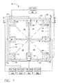
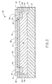
- FIG. 1 An embodiment of a Hall-effect element 20 according to the present invention is shown in Figs. 1 and 2 .
- the element 20 includes an isolating layer 22 and an active layer 24 of a first conductivity type disposed on the isolating layer 22.
- the layer 24 has a surface 26.
- An insulating layer 28 is disposed on the layer 24 over a substantial portion of the surface 26.
- a first set of contacts 30, 32 is disposed in contact with the surface 26 of the layer 24 along a first axis 34
- a second set of contacts 36, 38 is disposed in contact with the surface 26 of the layer 24 along a second axis 40 transverse to the first axis 34.
- four metal control field plates 42, 44, 46, 48 Disposed on the layer 28 are four metal control field plates 42, 44, 46, 48 which are each preferably selectively and individually coupleable to a voltage source 50a, 50b, 50c, 50d.
- the voltage sources 50a, 50b, 50c, 50d can have predetermined, fixed voltages; alternatively, the voltage sources 50a, 50b, 50c, 50d can have variable voltages, initially set to a predetermined voltage and varying therefrom in accordance with changes in operating conditions.
- voltage is applied to the control field plates 42, 44, 46, 48 to vary the accumulation of charge carriers at the surface 26 of the layer 24 (i.e., attract or repel the charge carriers).
- the resistance of the layer 24 can be varied. That is, if more charge carriers are available in a given region, then the resistance of the layer 24 in that region will decrease; conversely, if fewer charge carriers are available, then the resistance of the layer 24 will increase.
- a substantially null at zero applied magnetic field can be achieved.
- control field plates 42, 44, 46, 48 are used in the embodiment of the element 20 according to the present invention to allow for greater selectivity in the control of the resistance of the layer 24.
- the number of control field plates can vary according to the degree to which control of local resistance is desired.
- the method and apparatus by which voltage compensation is provided in element 20 has several advantages.
- the charge carriers accumulated at the surface 26 of the layer 24 as a result of voltage applied to the control plates 42, 44, 46, 48 should have similar mobility as the charge carriers in other regions of the layer 24, thereby providing inherent temperature compensation. Further, the size and complexity of the compensation circuitry is reduced over that conventionally used.
- the isolating layer 22 is preferably a p-type silicon
- the active layer 24 is preferably an n-type epitaxial silicon layer that is grown on the isolating layer 22.
- the layer 22 can be silicon dioxide (SiO 2 )
- the layer 24 may be a p-type silicon or any semiconductor material, such as gallium arsenide.
- the active layer 24 has an active region 52 preferably bounded by diffusion of p-type charge carriers into a boundary region 54 at an outer edge 56 of the active region 52.
- the boundary region 54 can be silicon dioxide (SiO 2 ).
- the active region 52 has a square-shape with sides 58, 60, 62, 64, although other geometries (e.g., rectangular or truncated square or rectangular) are possible.
- the insulating layer 28 for example, a p-type silicon or an insulator, such as silicon dioxide (SiO 2 )) is grown over the active layer 24.
- the first set of contacts 30, 32 is deposited over the insulating layer 28 along the first axis 34 in contact with heavily doped regions 66, 68 of the layer 24 having the same type as the layer 24, thus defining a low-resistance contact.
- Fig. 2 shows one of the ohmic contact regions 70 between the contact 30 and the doped region 66.
- the second set of contacts 36, 38 are deposited over the insulating layer 28 along the second axis 40 in contact with doped regions 72, 74, defining ohmic contact regions, one of which is shown as 76.
- the first and second axes 34, 40 define the diagonals of the square-shaped active region 52, and are thus substantially orthogonal to each other.
- each of the shield plates 78, 80, 82, 84 covers a separate quadrant of the square-shaped active region 52, and each is preferably connected to a separate terminal, which can be coupled, for example to ground or V cc .
- a single-shield plate can be used, or all of the plates can be connected to a single terminal.
- control field plates 42, 44, 46, 48 are deposited on the insulating layer 28, each plate along a different side 58, 60, 62, 64 of the square-shaped active region 52.
- the control field plates 42, 44, 46, 48 are spaced from each other and from the shield plates 78, 80, 82, 84.
- the control field plates 42, 44, 46, 48 form MOS capacitor structures, and voltage applied to the control field plates 42, 44, 46, 48 controls the accumulation of charge carriers on the surface 26 under the insulating layer 28.
- positive surface state charges are formed at the oxide-layer interface 26 ( Fig. 2 ).
- Positive voltages applied to the control field plates 42, 44, 46, 48 increase the accumulation of n-type charge carriers at the surface 26 and thereby decrease a local resistance in a corresponding region of the layer 24 proximate to the control field plates 42, 44, 46, 48; negative voltages decrease the accumulation charge carriers and thereby increase resistance.
- the first set of contacts 30, 32 is coupled to a voltage source 86, as shown.
- a magnetic field is applied perpendicularly to the Hall-effect element 20
- the flow of charge carriers is skewed in the plane of the layer 24 and is perpendicular to the flow of current between the first set of contacts 30, 32.
- the resultant field produces an output voltage between the second set of contacts 36, 38.
- the output voltage increases linearly with voltage applied across the first set of contacts 30, 32 and the strength of the magnetic field, and is positive or negative depending on the polarity of the magnetic field.
- the voltage between the second set of contacts 36, 38 can include an offset voltage component.
- the offset voltage is caused by local resistance variations due to fabrication flaws and material stresses, for example.
- voltage is applied to one or more of the control field plates 42, 44, 46, 48 to vary the local resistances in the corresponding regions by varying the accumulation of charge carriers at the surface 26.
- the shape and size of the plates 42, 44, 46, 48 can be selected to assist in the control of the local resistances. In this manner, the offset voltage can be reduced to substantially zero.
- FIG. 3 an alternative representation for the Hall-effect element 20 is shown in Fig. 3 .
- a Wheatstone bridge equivalent circuit 88 for the Hall-effect element 20 is shown.
- the control field plates 42, 44, 46, 48 are used to vary the local resistances R1, R2, R3, R4 so that the output for zero magnetic field is substantially zero (i.e., the bridge is balanced).
Landscapes
- Physics & Mathematics (AREA)
- Condensed Matter Physics & Semiconductors (AREA)
- General Physics & Mathematics (AREA)
- Hall/Mr Elements (AREA)
- Control Of Motors That Do Not Use Commutators (AREA)
Claims (14)
- Hall-Effekt-Element, umfassend:eine Isolierschicht (22);eine aktive Schicht (24) eines ersten elektrischen Leitfähigkeitstyps, auf der Isolierschicht angeordnet und mit einer Oberfläche (26);eine erste Menge von Kontakten (30, 32), in Kontakt mit der Oberfläche entlang einer ersten Achse (34) angeordnet;eine zweite Menge von Kontakten (36, 38), in Kontakt mit der Oberfläche entlang einer quer zur ersten Achse verlaufenden zweiten Achse (40) angeordnet;eine auf der Oberfläche angeordnete Isolierschicht (28) undeine Metallsteuerfeldplatte (42, 44, 46, 48), auf der Isolierschicht angeordnet, um einen Kondensator zu bilden, wobei die Metallsteuerfeldplatte an eine Spannungsquelle gekoppelt werden kann, um die Akkumulation von Ladungsträgern an der Oberfläche der aktiven Schicht zu steuern, um den Widerstand der aktiven Schicht zu variieren; gekennzeichnet durch:eine Abschirmplatte, auf der Isolierschicht (28) angeordnet, wobei die Abschirmplatte von der ersten und zweiten Menge von Kontakten und der Metallsteuerfeldplatte beabstandet ist und im wesentlichen alle Abschnitte der aktiven Schicht (24) bedeckt, die nicht von der Metallsteuerfeldplatte und der ersten und zweiten Menge von Kontakten bedeckt sind, um die Oberfläche (26) abzuschirmen.
- Hall-Effekt-Element nach Anspruch 1, umfassend vier Metallsteuerfeldplatten (42, 44, 46, 48), wobei jede Platte individuell an eine Spannungsquelle (50a, 50b, 50c, 50d) gekoppelt werden kann, um die Akkumulation von Ladungsträgern an der Oberfläche der aktiven Schicht zu steuern, um einen lokalen Widerstand der aktiven Schicht (24) jeder Platte benachbart zu variieren.
- Hall-Effekt-Element nach Anspruch 2, weiterhin umfassend ein Grenzgebiet (54), in dem Ladungsträger eines zweiten elektrischen Leitfähigkeitstyps in die aktive Schicht (24) vom ersten elektrischen Leitfähigkeitstyp diffundiert werden, wobei das Grenzgebiet ein hypothetisches quadrat-förmiges aktives Gebiet (52) mit vier Ecken und vier Seiten (58, 60, 62, 64) definiert, wobei die erste und zweite Menge von Kontakten (30, 32; 36, 38) an gegenüberliegenden Ecken des quadrat-förmigen aktiven Gebiets entlang jeweiliger Diagonalen des quadrat-förmigen aktiven Gebiets angeordnet sind und die vier Metallplatten (42, 44, 46, 48) entlang der Seiten des quadrat-förmigen aktiven Gebiets angeordnet sind.
- Hall-Effekt-Element nach Anspruch 3, umfassend vier Metallabschirmplatten (78, 80, 82, 84), die direkt auf der Isolierschicht angeordnet sind, wobei die Metallabschirmplatten voneinander und von den Metallsteuerfeldplatten (42, 44, 46, 48) beabstandet sind.
- Hall-Effekt-Element nach Anspruch 4, wobei die Isolierschicht (22) ein Material vom p-Typ umfaßt und die aktive Schicht (24) ein Material vom n-Typ umfaßt.
- Hall-Effekt-Element nach Anspruch 4, wobei die erste und zweite Achse (34; 40) orthogonal verlaufen.
- Hall-Effekt-Element nach Anspruch 4, wobei in die aktive Schicht (24) bei einem ersten elektrischen Leitfähigkeitstyp in dem Grenzgebiet (54) diffundierte Ladungsträger Ladungsträger vom p-Typ umfassen.
- Hall-Effekt-Element nach Anspruch 4, wobei die Isolierschicht (28) Siliziumdioxid umfaßt.
- Hall-Effekt-Element nach Anspruch 4, wobei die Metallabschirmplatten (78, 80, 82, 84) Aluminiumplatten umfassen.
- Hall-Effekt-Vorrichtung, umfassend:ein Hall-Effekt-Element nach einem der vorhergehenden Ansprüche.
- Verfahren zum Reduzieren eines Null-Offset in einem Hall-Effekt-Element, wobei das Verfahren die folgenden Schritte umfaßt:Bereitstellen einer Isolierschicht (22);Anordnen einer aktiven Schicht (24) von einem ersten Leitfähigkeitstyp auf der Isolierschicht, wobei die aktive Schicht eine Oberfläche (26) aufweist;Anordnen einer ersten Menge von Kontakten (30, 32) auf der Oberfläche entlang einer ersten Achse (34) ;Anordnen einer zweiten Menge von Kontakten (36, 38) auf der Oberfläche entlang einer quer zur ersten Achse verlaufenden zweiten Achse (40);Anordnen einer Isolierschicht (28) auf der Oberfläche undAnordnen einer Elektrode auf der Isolierschicht, wobei die Elektrode, die Isolierschicht und die aktive Schicht einen Kondensator bilden; so daß eine Spannung an den Kondensator angelegt werden kann, um die Akkumulation von Ladungsträgern an der Oberfläche zu steuern, um den Widerstand der aktiven Schicht zu variieren, wobei das Verfahren gekennzeichnet ist durch
Bereitstellen einer Abschirmplatte auf der Isolierschicht (28), wobei die Abschirmplatte von der ersten und zweiten Menge von Kontakten und der Steuerelektrode beabstandet ist und im wesentlichen alle Abschnitte der aktiven Schicht (24) bedeckt, die nicht von der Steuerelektrode und der ersten und zweiten Menge von Kontakten bedeckt sind, um die Oberfläche (26) abzuschirmen. - Verfahren nach Anspruch 11, wobei:der Schritt des Bereitstellens einer Isolierschicht (22) das Bereitstellen einer Schicht vom p-Typ umfaßt,der Schritt des Anordnens einer aktiven Schicht (24) das Anordnen einer Schicht vom n-Typ auf der Schicht vom p-Typ umfaßt undder Schritt des Anlegens einer Spannung das Anlegen einer positiven Spannung an die Isolierschicht (28) umfaßt, um die Akkumulation von Ladungsträgern vom n-Typ an der Oberfläche zu erhöhen, um den Widerstand der aktiven Schicht zu senken.
- Verfahren nach Anspruch 11, wobei:der Schritt des Bereitstellens einer Isolierschicht (22) das Bereitstellen einer Schicht vom p-Typ umfaßt,der Schritt des Anordnens einer aktiven Schicht (24) das Anordnen einer Schicht vom n-Typ auf der Schicht vom p-Typ umfaßt undder Schritt des Anlegens einer Spannung das Anlegen einer negativen Spannung an die Isolierschicht umfaßt, um die Akkumulation von Ladungsträgern vom n-Typ an der Oberfläche zu senken, um den Widerstand der aktiven Schicht zu erhöhen.
- Verfahren nach Anspruch 11, wobei der Schritt des Anlegens einer Spannung das Anlegen mehrerer Spannungen an verschiedene Gebiete der Isolierschicht (28) umfaßt, um die Akkumulation von Ladungsträgern an der Oberfläche (26) zu steuern, um einen lokalen Widerstand in jedem der verschiedenen Gebiete zu variieren.
Applications Claiming Priority (3)
| Application Number | Priority Date | Filing Date | Title |
|---|---|---|---|
| US542213 | 2000-04-04 | ||
| US09/542,213 US6492697B1 (en) | 2000-04-04 | 2000-04-04 | Hall-effect element with integrated offset control and method for operating hall-effect element to reduce null offset |
| PCT/US2001/010951 WO2001074139A2 (en) | 2000-04-04 | 2001-04-04 | Hall-effect element with integrated offset control and method for operating hall-effect element to reduce null offset |
Publications (2)
| Publication Number | Publication Date |
|---|---|
| EP1269552A2 EP1269552A2 (de) | 2003-01-02 |
| EP1269552B1 true EP1269552B1 (de) | 2008-07-16 |
Family
ID=24162811
Family Applications (1)
| Application Number | Title | Priority Date | Filing Date |
|---|---|---|---|
| EP01924664A Expired - Lifetime EP1269552B1 (de) | 2000-04-04 | 2001-04-04 | Hall-effekt element mit integrierter abweichungsregelung und verfahren zum betreiben eines solchen elements zur reduzierung der nullpunktabweichung |
Country Status (7)
| Country | Link |
|---|---|
| US (1) | US6492697B1 (de) |
| EP (1) | EP1269552B1 (de) |
| JP (1) | JP2003532279A (de) |
| AT (1) | ATE401671T1 (de) |
| CA (1) | CA2405149A1 (de) |
| DE (1) | DE60134839D1 (de) |
| WO (1) | WO2001074139A2 (de) |
Families Citing this family (72)
| Publication number | Priority date | Publication date | Assignee | Title |
|---|---|---|---|---|
| US7872322B2 (en) * | 2002-09-10 | 2011-01-18 | Melexis Tessenderlo Nv | Magnetic field sensor with a hall element |
| JP2004207477A (ja) * | 2002-12-25 | 2004-07-22 | Sanken Electric Co Ltd | ホール素子を有する半導体装置 |
| NL1024114C1 (nl) * | 2003-08-15 | 2005-02-16 | Systematic Design Holding B V | Werkwijze en inrichting voor het verrichten van metingen aan magnetische velden met gebruik van een hall-sensor. |
| US7015557B2 (en) * | 2004-04-16 | 2006-03-21 | Honeywell International Inc. | Hall element with segmented field plate |
| US7002229B2 (en) * | 2004-06-16 | 2006-02-21 | Honeywell International Inc. | Self aligned Hall with field plate |
| US7019517B2 (en) * | 2004-07-20 | 2006-03-28 | Honeywell International Inc. | Offset magnet rotary position sensor |
| JP4039436B2 (ja) * | 2004-08-06 | 2008-01-30 | 株式会社デンソー | 回転角検出装置 |
| US7019607B2 (en) * | 2004-08-09 | 2006-03-28 | Honeywell International Inc. | Precision non-contact digital switch |
| US7173412B2 (en) | 2004-11-30 | 2007-02-06 | Honeywell International Inc. | Quadrature sensor systems and methods |
| US8266982B2 (en) | 2005-01-18 | 2012-09-18 | Kongsberg Automotive Holding Asa, Inc. | Method and apparatus for pedal hysteresis |
| US7205622B2 (en) * | 2005-01-20 | 2007-04-17 | Honeywell International Inc. | Vertical hall effect device |
| US7271584B2 (en) * | 2005-07-09 | 2007-09-18 | Honeywell International Inc. | Magnetic sensing apparatus |
| US7573112B2 (en) | 2006-04-14 | 2009-08-11 | Allegro Microsystems, Inc. | Methods and apparatus for sensor having capacitor on chip |
| US7687882B2 (en) | 2006-04-14 | 2010-03-30 | Allegro Microsystems, Inc. | Methods and apparatus for integrated circuit having multiple dies with at least one on chip capacitor |
| US7382120B2 (en) * | 2006-04-26 | 2008-06-03 | Honeywell International Inc. | Rotary position sensor with rectangular magnet and hall sensors placed in association with the surface of the magnet |
| US7389685B2 (en) * | 2006-06-13 | 2008-06-24 | Honeywell International Inc. | Downhole pressure transmitter |
| US20080013298A1 (en) | 2006-07-14 | 2008-01-17 | Nirmal Sharma | Methods and apparatus for passive attachment of components for integrated circuits |
| GB0723973D0 (en) * | 2007-12-07 | 2008-01-16 | Melexis Nv | Hall sensor array |
| US9823090B2 (en) | 2014-10-31 | 2017-11-21 | Allegro Microsystems, Llc | Magnetic field sensor for sensing a movement of a target object |
| US7772661B2 (en) * | 2008-07-23 | 2010-08-10 | Honeywell International Inc. | Hall-effect magnetic sensors with improved magnetic responsivity and methods for manufacturing the same |
| US8624588B2 (en) | 2008-07-31 | 2014-01-07 | Allegro Microsystems, Llc | Apparatus and method for providing an output signal indicative of a speed of rotation and a direction of rotation as a ferromagnetic object |
| JP5998380B2 (ja) * | 2011-03-07 | 2016-09-28 | 国立研究開発法人産業技術総合研究所 | 半導体基板、半導体装置および半導体基板の製造方法 |
| US8629539B2 (en) | 2012-01-16 | 2014-01-14 | Allegro Microsystems, Llc | Methods and apparatus for magnetic sensor having non-conductive die paddle |
| US9812588B2 (en) | 2012-03-20 | 2017-11-07 | Allegro Microsystems, Llc | Magnetic field sensor integrated circuit with integral ferromagnetic material |
| US9494660B2 (en) | 2012-03-20 | 2016-11-15 | Allegro Microsystems, Llc | Integrated circuit package having a split lead frame |
| US10234513B2 (en) | 2012-03-20 | 2019-03-19 | Allegro Microsystems, Llc | Magnetic field sensor integrated circuit with integral ferromagnetic material |
| US9666788B2 (en) | 2012-03-20 | 2017-05-30 | Allegro Microsystems, Llc | Integrated circuit package having a split lead frame |
| US9817078B2 (en) | 2012-05-10 | 2017-11-14 | Allegro Microsystems Llc | Methods and apparatus for magnetic sensor having integrated coil |
| US9484525B2 (en) * | 2012-05-15 | 2016-11-01 | Infineon Technologies Ag | Hall effect device |
| US8754640B2 (en) | 2012-06-18 | 2014-06-17 | Allegro Microsystems, Llc | Magnetic field sensors and related techniques that can provide self-test information in a formatted output signal |
| US9411025B2 (en) | 2013-04-26 | 2016-08-09 | Allegro Microsystems, Llc | Integrated circuit package having a split lead frame and a magnet |
| KR102019514B1 (ko) * | 2013-06-28 | 2019-11-15 | 매그나칩 반도체 유한회사 | 반도체 기반의 홀 센서 |
| US10495699B2 (en) | 2013-07-19 | 2019-12-03 | Allegro Microsystems, Llc | Methods and apparatus for magnetic sensor having an integrated coil or magnet to detect a non-ferromagnetic target |
| US9810519B2 (en) | 2013-07-19 | 2017-11-07 | Allegro Microsystems, Llc | Arrangements for magnetic field sensors that act as tooth detectors |
| US10145908B2 (en) | 2013-07-19 | 2018-12-04 | Allegro Microsystems, Llc | Method and apparatus for magnetic sensor producing a changing magnetic field |
| US9720054B2 (en) | 2014-10-31 | 2017-08-01 | Allegro Microsystems, Llc | Magnetic field sensor and electronic circuit that pass amplifier current through a magnetoresistance element |
| US9823092B2 (en) | 2014-10-31 | 2017-11-21 | Allegro Microsystems, Llc | Magnetic field sensor providing a movement detector |
| US10712403B2 (en) | 2014-10-31 | 2020-07-14 | Allegro Microsystems, Llc | Magnetic field sensor and electronic circuit that pass amplifier current through a magnetoresistance element |
| US9719806B2 (en) | 2014-10-31 | 2017-08-01 | Allegro Microsystems, Llc | Magnetic field sensor for sensing a movement of a ferromagnetic target object |
| JP6612887B2 (ja) * | 2015-09-24 | 2019-11-27 | 旭化成エレクトロニクス株式会社 | ホール素子及びホールセンサ、レンズモジュール |
| JP6608666B2 (ja) * | 2015-10-16 | 2019-11-20 | 旭化成エレクトロニクス株式会社 | ホール素子及びホールセンサ、レンズモジュール |
| US10411498B2 (en) | 2015-10-21 | 2019-09-10 | Allegro Microsystems, Llc | Apparatus and methods for extending sensor integrated circuit operation through a power disturbance |
| US10495700B2 (en) | 2016-01-29 | 2019-12-03 | Allegro Microsystems, Llc | Method and system for providing information about a target object in a formatted output signal |
| EP4067908B1 (de) | 2016-05-17 | 2025-11-12 | Allegro MicroSystems, LLC | Magnetfeldsensor und verfahren zum betreiben eines magnetfeldsensors |
| US10012518B2 (en) | 2016-06-08 | 2018-07-03 | Allegro Microsystems, Llc | Magnetic field sensor for sensing a proximity of an object |
| US10260905B2 (en) | 2016-06-08 | 2019-04-16 | Allegro Microsystems, Llc | Arrangements for magnetic field sensors to cancel offset variations |
| US10041810B2 (en) | 2016-06-08 | 2018-08-07 | Allegro Microsystems, Llc | Arrangements for magnetic field sensors that act as movement detectors |
| US11029372B2 (en) * | 2016-11-18 | 2021-06-08 | Asahi Kasei Microdevices Corporation | Hall element for mitigating current concentration and fabrication method thereof |
| JP7015087B2 (ja) * | 2017-03-23 | 2022-02-02 | 旭化成エレクトロニクス株式会社 | ホール素子 |
| US10837943B2 (en) | 2017-05-26 | 2020-11-17 | Allegro Microsystems, Llc | Magnetic field sensor with error calculation |
| US11428755B2 (en) | 2017-05-26 | 2022-08-30 | Allegro Microsystems, Llc | Coil actuated sensor with sensitivity detection |
| US10641842B2 (en) | 2017-05-26 | 2020-05-05 | Allegro Microsystems, Llc | Targets for coil actuated position sensors |
| US10324141B2 (en) | 2017-05-26 | 2019-06-18 | Allegro Microsystems, Llc | Packages for coil actuated position sensors |
| US10996289B2 (en) | 2017-05-26 | 2021-05-04 | Allegro Microsystems, Llc | Coil actuated position sensor with reflected magnetic field |
| US10310028B2 (en) | 2017-05-26 | 2019-06-04 | Allegro Microsystems, Llc | Coil actuated pressure sensor |
| US10866117B2 (en) | 2018-03-01 | 2020-12-15 | Allegro Microsystems, Llc | Magnetic field influence during rotation movement of magnetic target |
| US10978897B2 (en) | 2018-04-02 | 2021-04-13 | Allegro Microsystems, Llc | Systems and methods for suppressing undesirable voltage supply artifacts |
| US10656170B2 (en) | 2018-05-17 | 2020-05-19 | Allegro Microsystems, Llc | Magnetic field sensors and output signal formats for a magnetic field sensor |
| US11255700B2 (en) | 2018-08-06 | 2022-02-22 | Allegro Microsystems, Llc | Magnetic field sensor |
| US10823586B2 (en) | 2018-12-26 | 2020-11-03 | Allegro Microsystems, Llc | Magnetic field sensor having unequally spaced magnetic field sensing elements |
| US11061084B2 (en) | 2019-03-07 | 2021-07-13 | Allegro Microsystems, Llc | Coil actuated pressure sensor and deflectable substrate |
| US11588101B2 (en) * | 2019-03-30 | 2023-02-21 | Texas Instruments Incorporated | Hall sensor with performance control |
| US10955306B2 (en) | 2019-04-22 | 2021-03-23 | Allegro Microsystems, Llc | Coil actuated pressure sensor and deformable substrate |
| US10991644B2 (en) | 2019-08-22 | 2021-04-27 | Allegro Microsystems, Llc | Integrated circuit package having a low profile |
| US11280637B2 (en) | 2019-11-14 | 2022-03-22 | Allegro Microsystems, Llc | High performance magnetic angle sensor |
| US11237020B2 (en) | 2019-11-14 | 2022-02-01 | Allegro Microsystems, Llc | Magnetic field sensor having two rows of magnetic field sensing elements for measuring an angle of rotation of a magnet |
| US11372061B2 (en) | 2020-03-13 | 2022-06-28 | Globalfoundries Singapore Pte. Ltd. | Hall effect sensor devices and methods of forming hall effect sensor devices |
| US11262422B2 (en) | 2020-05-08 | 2022-03-01 | Allegro Microsystems, Llc | Stray-field-immune coil-activated position sensor |
| US11493361B2 (en) | 2021-02-26 | 2022-11-08 | Allegro Microsystems, Llc | Stray field immune coil-activated sensor |
| US11578997B1 (en) | 2021-08-24 | 2023-02-14 | Allegro Microsystems, Llc | Angle sensor using eddy currents |
| US12449279B2 (en) | 2024-02-07 | 2025-10-21 | Allegro Microsystems, Llc | Dynamic resolution sensor |
| US12523717B2 (en) | 2024-02-15 | 2026-01-13 | Allegro Microsystems, Llc | Closed loop magnetic field sensor with current control |
Family Cites Families (8)
| Publication number | Priority date | Publication date | Assignee | Title |
|---|---|---|---|---|
| US3825777A (en) * | 1973-02-14 | 1974-07-23 | Ibm | Hall cell with offset voltage control |
| US4660065A (en) * | 1983-06-10 | 1987-04-21 | Texas Instruments Incorporated | Hall effect device with surface potential shielding layer |
| CH668146A5 (de) | 1985-05-22 | 1988-11-30 | Landis & Gyr Ag | Einrichtung mit einem hallelement in integrierter halbleitertechnologie. |
| JPS6385487A (ja) * | 1986-09-30 | 1988-04-15 | Toshiba Corp | 放射線検出器 |
| JPH01162386A (ja) * | 1987-12-18 | 1989-06-26 | Matsushita Electron Corp | ホール素子 |
| JP3602611B2 (ja) | 1995-03-30 | 2004-12-15 | 株式会社東芝 | 横型ホール素子 |
| JPH10270773A (ja) | 1997-03-26 | 1998-10-09 | Toshiba Corp | ホール素子 |
| JP3592499B2 (ja) | 1997-09-09 | 2004-11-24 | 株式会社東芝 | ホール素子 |
-
2000
- 2000-04-04 US US09/542,213 patent/US6492697B1/en not_active Expired - Lifetime
-
2001
- 2001-04-04 AT AT01924664T patent/ATE401671T1/de not_active IP Right Cessation
- 2001-04-04 DE DE60134839T patent/DE60134839D1/de not_active Expired - Lifetime
- 2001-04-04 EP EP01924664A patent/EP1269552B1/de not_active Expired - Lifetime
- 2001-04-04 CA CA002405149A patent/CA2405149A1/en not_active Abandoned
- 2001-04-04 WO PCT/US2001/010951 patent/WO2001074139A2/en not_active Ceased
- 2001-04-04 JP JP2001571905A patent/JP2003532279A/ja not_active Withdrawn
Also Published As
| Publication number | Publication date |
|---|---|
| US6492697B1 (en) | 2002-12-10 |
| CA2405149A1 (en) | 2001-10-11 |
| WO2001074139A2 (en) | 2001-10-11 |
| DE60134839D1 (de) | 2008-08-28 |
| WO2001074139A3 (en) | 2002-09-26 |
| ATE401671T1 (de) | 2008-08-15 |
| EP1269552A2 (de) | 2003-01-02 |
| JP2003532279A (ja) | 2003-10-28 |
Similar Documents
| Publication | Publication Date | Title |
|---|---|---|
| EP1269552B1 (de) | Hall-effekt element mit integrierter abweichungsregelung und verfahren zum betreiben eines solchen elements zur reduzierung der nullpunktabweichung | |
| KR940001298B1 (ko) | 집적회로에 집적가능한 홀소자를 구비한 장치 | |
| US7626377B2 (en) | Hall-effect device with merged and/or non-merged complementary structure | |
| US4673964A (en) | Buried Hall element | |
| EP0623951B1 (de) | Halbleiteranordnung in einer dünnen aktiven Schicht mit hoher Durchbruchspannung | |
| US4945762A (en) | Silicon sensor with trimmable wheatstone bridge | |
| US4618875A (en) | Darlington transistor circuit | |
| US20100019331A1 (en) | Hall-effect magnetic sensors with improved magnetic responsivity and methods for manufacturing the same | |
| US4631562A (en) | Zener diode structure | |
| US4053915A (en) | Temperature compensated constant current source device | |
| JPH09507370A (ja) | 保護形スイッチ | |
| US4660065A (en) | Hall effect device with surface potential shielding layer | |
| JPH0230588B2 (de) | ||
| EP0625797B1 (de) | Integrierte Struktur eines Strom-Fühlwiderstandes für Leistungs-MOSFET-Vorrichtungen, insbesondere für Leistungs-MOSFET-Vorrichtungen mit einer Überstrom-Selbst-Schutzschaltung | |
| US5293051A (en) | Photoswitching device including a MOSFET for detecting zero voltage crossing | |
| US3994010A (en) | Hall effect elements | |
| CA1220874A (en) | Integrated circuit with stress isolated hall element | |
| US4651178A (en) | Dual inverse zener diode with buried junctions | |
| EP3915154A1 (de) | Halbleiterbauelemente mit isolator-metall-speicherstoffen | |
| US10121846B1 (en) | Resistor structure with high resistance based on very thin semiconductor layer | |
| US5920106A (en) | Semiconductor device and method for producing the same | |
| US6013934A (en) | Semiconductor structure for thermal shutdown protection | |
| US4223335A (en) | Semiconductor device body having identical isolated composite resistor regions | |
| EP0083060A2 (de) | Halbleiteranordnung mit Überspannungsschutzdiode | |
| US4942446A (en) | Semiconductor device for switching, and the manufacturing method therefor |
Legal Events
| Date | Code | Title | Description |
|---|---|---|---|
| PUAI | Public reference made under article 153(3) epc to a published international application that has entered the european phase |
Free format text: ORIGINAL CODE: 0009012 |
|
| 17P | Request for examination filed |
Effective date: 20021003 |
|
| AK | Designated contracting states |
Kind code of ref document: A2 Designated state(s): AT BE CH CY DE DK ES FI FR GB GR IE IT LI LU MC NL PT SE TR |
|
| 17Q | First examination report despatched |
Effective date: 20060717 |
|
| GRAP | Despatch of communication of intention to grant a patent |
Free format text: ORIGINAL CODE: EPIDOSNIGR1 |
|
| GRAS | Grant fee paid |
Free format text: ORIGINAL CODE: EPIDOSNIGR3 |
|
| GRAA | (expected) grant |
Free format text: ORIGINAL CODE: 0009210 |
|
| AK | Designated contracting states |
Kind code of ref document: B1 Designated state(s): AT BE CH CY DE DK ES FI FR GB GR IE IT LI LU MC NL PT SE TR |
|
| REG | Reference to a national code |
Ref country code: GB Ref legal event code: FG4D |
|
| REG | Reference to a national code |
Ref country code: CH Ref legal event code: EP |
|
| REF | Corresponds to: |
Ref document number: 60134839 Country of ref document: DE Date of ref document: 20080828 Kind code of ref document: P |
|
| REG | Reference to a national code |
Ref country code: IE Ref legal event code: FG4D |
|
| NLV1 | Nl: lapsed or annulled due to failure to fulfill the requirements of art. 29p and 29m of the patents act | ||
| PG25 | Lapsed in a contracting state [announced via postgrant information from national office to epo] |
Ref country code: PT Free format text: LAPSE BECAUSE OF FAILURE TO SUBMIT A TRANSLATION OF THE DESCRIPTION OR TO PAY THE FEE WITHIN THE PRESCRIBED TIME-LIMIT Effective date: 20081216 Ref country code: NL Free format text: LAPSE BECAUSE OF FAILURE TO SUBMIT A TRANSLATION OF THE DESCRIPTION OR TO PAY THE FEE WITHIN THE PRESCRIBED TIME-LIMIT Effective date: 20080716 Ref country code: ES Free format text: LAPSE BECAUSE OF FAILURE TO SUBMIT A TRANSLATION OF THE DESCRIPTION OR TO PAY THE FEE WITHIN THE PRESCRIBED TIME-LIMIT Effective date: 20081027 |
|
| PG25 | Lapsed in a contracting state [announced via postgrant information from national office to epo] |
Ref country code: FI Free format text: LAPSE BECAUSE OF FAILURE TO SUBMIT A TRANSLATION OF THE DESCRIPTION OR TO PAY THE FEE WITHIN THE PRESCRIBED TIME-LIMIT Effective date: 20080716 Ref country code: AT Free format text: LAPSE BECAUSE OF FAILURE TO SUBMIT A TRANSLATION OF THE DESCRIPTION OR TO PAY THE FEE WITHIN THE PRESCRIBED TIME-LIMIT Effective date: 20080716 |
|
| PG25 | Lapsed in a contracting state [announced via postgrant information from national office to epo] |
Ref country code: BE Free format text: LAPSE BECAUSE OF FAILURE TO SUBMIT A TRANSLATION OF THE DESCRIPTION OR TO PAY THE FEE WITHIN THE PRESCRIBED TIME-LIMIT Effective date: 20080716 |
|
| PG25 | Lapsed in a contracting state [announced via postgrant information from national office to epo] |
Ref country code: DK Free format text: LAPSE BECAUSE OF FAILURE TO SUBMIT A TRANSLATION OF THE DESCRIPTION OR TO PAY THE FEE WITHIN THE PRESCRIBED TIME-LIMIT Effective date: 20080716 |
|
| PLBE | No opposition filed within time limit |
Free format text: ORIGINAL CODE: 0009261 |
|
| STAA | Information on the status of an ep patent application or granted ep patent |
Free format text: STATUS: NO OPPOSITION FILED WITHIN TIME LIMIT |
|
| 26N | No opposition filed |
Effective date: 20090417 |
|
| PG25 | Lapsed in a contracting state [announced via postgrant information from national office to epo] |
Ref country code: IT Free format text: LAPSE BECAUSE OF FAILURE TO SUBMIT A TRANSLATION OF THE DESCRIPTION OR TO PAY THE FEE WITHIN THE PRESCRIBED TIME-LIMIT Effective date: 20080716 |
|
| REG | Reference to a national code |
Ref country code: CH Ref legal event code: PL |
|
| PG25 | Lapsed in a contracting state [announced via postgrant information from national office to epo] |
Ref country code: CH Free format text: LAPSE BECAUSE OF NON-PAYMENT OF DUE FEES Effective date: 20090430 Ref country code: LI Free format text: LAPSE BECAUSE OF NON-PAYMENT OF DUE FEES Effective date: 20090430 Ref country code: SE Free format text: LAPSE BECAUSE OF FAILURE TO SUBMIT A TRANSLATION OF THE DESCRIPTION OR TO PAY THE FEE WITHIN THE PRESCRIBED TIME-LIMIT Effective date: 20081016 |
|
| PG25 | Lapsed in a contracting state [announced via postgrant information from national office to epo] |
Ref country code: MC Free format text: LAPSE BECAUSE OF NON-PAYMENT OF DUE FEES Effective date: 20090430 Ref country code: IE Free format text: LAPSE BECAUSE OF NON-PAYMENT OF DUE FEES Effective date: 20090404 |
|
| PG25 | Lapsed in a contracting state [announced via postgrant information from national office to epo] |
Ref country code: GR Free format text: LAPSE BECAUSE OF FAILURE TO SUBMIT A TRANSLATION OF THE DESCRIPTION OR TO PAY THE FEE WITHIN THE PRESCRIBED TIME-LIMIT Effective date: 20081017 |
|
| PG25 | Lapsed in a contracting state [announced via postgrant information from national office to epo] |
Ref country code: LU Free format text: LAPSE BECAUSE OF NON-PAYMENT OF DUE FEES Effective date: 20090404 |
|
| PG25 | Lapsed in a contracting state [announced via postgrant information from national office to epo] |
Ref country code: TR Free format text: LAPSE BECAUSE OF FAILURE TO SUBMIT A TRANSLATION OF THE DESCRIPTION OR TO PAY THE FEE WITHIN THE PRESCRIBED TIME-LIMIT Effective date: 20080716 |
|
| PG25 | Lapsed in a contracting state [announced via postgrant information from national office to epo] |
Ref country code: CY Free format text: LAPSE BECAUSE OF FAILURE TO SUBMIT A TRANSLATION OF THE DESCRIPTION OR TO PAY THE FEE WITHIN THE PRESCRIBED TIME-LIMIT Effective date: 20080716 |
|
| REG | Reference to a national code |
Ref country code: FR Ref legal event code: PLFP Year of fee payment: 16 |
|
| REG | Reference to a national code |
Ref country code: FR Ref legal event code: PLFP Year of fee payment: 17 |
|
| REG | Reference to a national code |
Ref country code: FR Ref legal event code: PLFP Year of fee payment: 18 |
|
| PGFP | Annual fee paid to national office [announced via postgrant information from national office to epo] |
Ref country code: FR Payment date: 20180426 Year of fee payment: 18 |
|
| PGFP | Annual fee paid to national office [announced via postgrant information from national office to epo] |
Ref country code: DE Payment date: 20180629 Year of fee payment: 18 Ref country code: GB Payment date: 20180427 Year of fee payment: 18 |
|
| REG | Reference to a national code |
Ref country code: DE Ref legal event code: R119 Ref document number: 60134839 Country of ref document: DE |
|
| GBPC | Gb: european patent ceased through non-payment of renewal fee |
Effective date: 20190404 |
|
| PG25 | Lapsed in a contracting state [announced via postgrant information from national office to epo] |
Ref country code: GB Free format text: LAPSE BECAUSE OF NON-PAYMENT OF DUE FEES Effective date: 20190404 Ref country code: DE Free format text: LAPSE BECAUSE OF NON-PAYMENT OF DUE FEES Effective date: 20191101 |
|
| PG25 | Lapsed in a contracting state [announced via postgrant information from national office to epo] |
Ref country code: FR Free format text: LAPSE BECAUSE OF NON-PAYMENT OF DUE FEES Effective date: 20190430 |