EP1269552B1 - Hall-effect element with integrated offset control and method for operating hall-effect element to reduce null offset - Google Patents
Hall-effect element with integrated offset control and method for operating hall-effect element to reduce null offset Download PDFInfo
- Publication number
- EP1269552B1 EP1269552B1 EP01924664A EP01924664A EP1269552B1 EP 1269552 B1 EP1269552 B1 EP 1269552B1 EP 01924664 A EP01924664 A EP 01924664A EP 01924664 A EP01924664 A EP 01924664A EP 1269552 B1 EP1269552 B1 EP 1269552B1
- Authority
- EP
- European Patent Office
- Prior art keywords
- layer
- hall
- effect element
- active layer
- contacts
- Prior art date
- Legal status (The legal status is an assumption and is not a legal conclusion. Google has not performed a legal analysis and makes no representation as to the accuracy of the status listed.)
- Expired - Lifetime
Links
- 230000005355 Hall effect Effects 0.000 title claims abstract description 49
- 238000000034 method Methods 0.000 title claims abstract description 15
- 239000002800 charge carrier Substances 0.000 claims abstract description 24
- 238000009825 accumulation Methods 0.000 claims abstract description 14
- 229910052751 metal Inorganic materials 0.000 claims abstract description 14
- 239000002184 metal Substances 0.000 claims abstract description 14
- VYPSYNLAJGMNEJ-UHFFFAOYSA-N Silicium dioxide Chemical compound O=[Si]=O VYPSYNLAJGMNEJ-UHFFFAOYSA-N 0.000 claims description 14
- 239000000377 silicon dioxide Substances 0.000 claims description 7
- 239000003990 capacitor Substances 0.000 claims description 5
- 239000000463 material Substances 0.000 claims description 4
- 235000012239 silicon dioxide Nutrition 0.000 claims description 4
- 229910052782 aluminium Inorganic materials 0.000 claims description 2
- XAGFODPZIPBFFR-UHFFFAOYSA-N aluminium Chemical compound [Al] XAGFODPZIPBFFR-UHFFFAOYSA-N 0.000 claims description 2
- XUIMIQQOPSSXEZ-UHFFFAOYSA-N Silicon Chemical compound [Si] XUIMIQQOPSSXEZ-UHFFFAOYSA-N 0.000 description 5
- 229910052710 silicon Inorganic materials 0.000 description 5
- 239000010703 silicon Substances 0.000 description 5
- 238000004519 manufacturing process Methods 0.000 description 3
- 230000000694 effects Effects 0.000 description 2
- JBRZTFJDHDCESZ-UHFFFAOYSA-N AsGa Chemical compound [As]#[Ga] JBRZTFJDHDCESZ-UHFFFAOYSA-N 0.000 description 1
- 229910001218 Gallium arsenide Inorganic materials 0.000 description 1
- 230000007850 degeneration Effects 0.000 description 1
- 230000001419 dependent effect Effects 0.000 description 1
- 238000009792 diffusion process Methods 0.000 description 1
- 230000005684 electric field Effects 0.000 description 1
- 239000012212 insulator Substances 0.000 description 1
- 239000004065 semiconductor Substances 0.000 description 1
- 230000035945 sensitivity Effects 0.000 description 1
- 239000000758 substrate Substances 0.000 description 1
Images

Classifications
-
- H—ELECTRICITY
- H10—SEMICONDUCTOR DEVICES; ELECTRIC SOLID-STATE DEVICES NOT OTHERWISE PROVIDED FOR
- H10N—ELECTRIC SOLID-STATE DEVICES NOT OTHERWISE PROVIDED FOR
- H10N52/00—Hall-effect devices
- H10N52/101—Semiconductor Hall-effect devices
-
- G—PHYSICS
- G01—MEASURING; TESTING
- G01R—MEASURING ELECTRIC VARIABLES; MEASURING MAGNETIC VARIABLES
- G01R33/00—Arrangements or instruments for measuring magnetic variables
- G01R33/02—Measuring direction or magnitude of magnetic fields or magnetic flux
- G01R33/06—Measuring direction or magnitude of magnetic fields or magnetic flux using galvano-magnetic devices
- G01R33/07—Hall effect devices
Definitions
- the present invention is directed generally to a Hall-effect element with offset control and a method for operating a Hall-effect element to reduce null offset, and, in particular, a Hall-effect element with integrated offset control and a method for operating a Hall-effect element having integrated offset control to reduce null offset.
- Hall-effect elements are well known in the art. Hall-effect elements rely on a reaction between a current flowing between a first set of contacts and an orthogonally-applied magnetic field to generate a voltage across a second set of contacts.
- null offset In theory, with no magnetic field applied to the Hall-effect element, no voltage should be generated across the second set of contacts. In practice, a voltage is typically generated across the second set of contacts even with no magnetic field applied to the Hall-effect element. This voltage is referred to as null offset.
- the trimmer network may include a current mirror with trimmable degeneration resistors.
- Trimmer networks come with their own set of associated problems. For example, Hall-effect elements are generally fabricated using a lightly doped n-type layer for heightened sensitivity to variations in magnetic field intensity. This means, however, that the element is also particularly sensitive to variations in temperature. As a consequence, the trimmer network must be able to adapt to the variations in resistance accompanying the variations in temperature. Furthermore, the subsequent amplifiers may also have variations with temperature which require compensation.
- One way to make the trimmer network responsive to variations in resistance accompanying the variations in temperature is to provide a large reference resistor in close thermal proximity to the device that requires temperature compensation.
- the reference resistor may be disposed in close proximity to the Hall-effect element, and coupled to the associated trimmer network.
- the trimmer network directs a portion of the current flowing through the reference resistor through the one of the Hall-effect element contacts to compensate for temperature-dependent changes in resistance. If variations occur in subsequent amplifiers or comparators, reference resistors must be provided for these devices as well.
- Another way to achieve temperature compensation involves using switches on the same chip as the Hall-effect element to direct current alternatively to the separate sets of Hall-effect element contacts.
- the output voltage difference between the two contacts is stored on a capacitor to allow subsequent compensations of the Hall-effect element.
- JP-A-10270773 describes a Hall-effect element having gate electrodes that form transistors with an active layer and supply electrodes and/or sense electrodes.
- EP-A-0735600 discloses a lateral Hall-effect element having a substrate, an active layer, supply electrodes contacting the active layer and sense electrodes contacting the active layer. Gate electrodes formed on the Hall-effect element control offset.
- US-A-4929993 discloses a Hall element incorporated in an integrated circuit.
- the present invention further provides a method for reducing null offset in a Hall-effect element, the method comprising the steps as defined in claim 11.
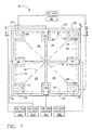
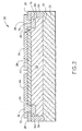
- FIG. 1 An embodiment of a Hall-effect element 20 according to the present invention is shown in Figs. 1 and 2 .
- the element 20 includes an isolating layer 22 and an active layer 24 of a first conductivity type disposed on the isolating layer 22.
- the layer 24 has a surface 26.
- An insulating layer 28 is disposed on the layer 24 over a substantial portion of the surface 26.
- a first set of contacts 30, 32 is disposed in contact with the surface 26 of the layer 24 along a first axis 34
- a second set of contacts 36, 38 is disposed in contact with the surface 26 of the layer 24 along a second axis 40 transverse to the first axis 34.
- four metal control field plates 42, 44, 46, 48 Disposed on the layer 28 are four metal control field plates 42, 44, 46, 48 which are each preferably selectively and individually coupleable to a voltage source 50a, 50b, 50c, 50d.
- the voltage sources 50a, 50b, 50c, 50d can have predetermined, fixed voltages; alternatively, the voltage sources 50a, 50b, 50c, 50d can have variable voltages, initially set to a predetermined voltage and varying therefrom in accordance with changes in operating conditions.
- voltage is applied to the control field plates 42, 44, 46, 48 to vary the accumulation of charge carriers at the surface 26 of the layer 24 (i.e., attract or repel the charge carriers).
- the resistance of the layer 24 can be varied. That is, if more charge carriers are available in a given region, then the resistance of the layer 24 in that region will decrease; conversely, if fewer charge carriers are available, then the resistance of the layer 24 will increase.
- a substantially null at zero applied magnetic field can be achieved.
- control field plates 42, 44, 46, 48 are used in the embodiment of the element 20 according to the present invention to allow for greater selectivity in the control of the resistance of the layer 24.
- the number of control field plates can vary according to the degree to which control of local resistance is desired.
- the method and apparatus by which voltage compensation is provided in element 20 has several advantages.
- the charge carriers accumulated at the surface 26 of the layer 24 as a result of voltage applied to the control plates 42, 44, 46, 48 should have similar mobility as the charge carriers in other regions of the layer 24, thereby providing inherent temperature compensation. Further, the size and complexity of the compensation circuitry is reduced over that conventionally used.
- the isolating layer 22 is preferably a p-type silicon
- the active layer 24 is preferably an n-type epitaxial silicon layer that is grown on the isolating layer 22.
- the layer 22 can be silicon dioxide (SiO 2 )
- the layer 24 may be a p-type silicon or any semiconductor material, such as gallium arsenide.
- the active layer 24 has an active region 52 preferably bounded by diffusion of p-type charge carriers into a boundary region 54 at an outer edge 56 of the active region 52.
- the boundary region 54 can be silicon dioxide (SiO 2 ).
- the active region 52 has a square-shape with sides 58, 60, 62, 64, although other geometries (e.g., rectangular or truncated square or rectangular) are possible.
- the insulating layer 28 for example, a p-type silicon or an insulator, such as silicon dioxide (SiO 2 )) is grown over the active layer 24.
- the first set of contacts 30, 32 is deposited over the insulating layer 28 along the first axis 34 in contact with heavily doped regions 66, 68 of the layer 24 having the same type as the layer 24, thus defining a low-resistance contact.
- Fig. 2 shows one of the ohmic contact regions 70 between the contact 30 and the doped region 66.
- the second set of contacts 36, 38 are deposited over the insulating layer 28 along the second axis 40 in contact with doped regions 72, 74, defining ohmic contact regions, one of which is shown as 76.
- the first and second axes 34, 40 define the diagonals of the square-shaped active region 52, and are thus substantially orthogonal to each other.
- each of the shield plates 78, 80, 82, 84 covers a separate quadrant of the square-shaped active region 52, and each is preferably connected to a separate terminal, which can be coupled, for example to ground or V cc .
- a single-shield plate can be used, or all of the plates can be connected to a single terminal.
- control field plates 42, 44, 46, 48 are deposited on the insulating layer 28, each plate along a different side 58, 60, 62, 64 of the square-shaped active region 52.
- the control field plates 42, 44, 46, 48 are spaced from each other and from the shield plates 78, 80, 82, 84.
- the control field plates 42, 44, 46, 48 form MOS capacitor structures, and voltage applied to the control field plates 42, 44, 46, 48 controls the accumulation of charge carriers on the surface 26 under the insulating layer 28.
- positive surface state charges are formed at the oxide-layer interface 26 ( Fig. 2 ).
- Positive voltages applied to the control field plates 42, 44, 46, 48 increase the accumulation of n-type charge carriers at the surface 26 and thereby decrease a local resistance in a corresponding region of the layer 24 proximate to the control field plates 42, 44, 46, 48; negative voltages decrease the accumulation charge carriers and thereby increase resistance.
- the first set of contacts 30, 32 is coupled to a voltage source 86, as shown.
- a magnetic field is applied perpendicularly to the Hall-effect element 20
- the flow of charge carriers is skewed in the plane of the layer 24 and is perpendicular to the flow of current between the first set of contacts 30, 32.
- the resultant field produces an output voltage between the second set of contacts 36, 38.
- the output voltage increases linearly with voltage applied across the first set of contacts 30, 32 and the strength of the magnetic field, and is positive or negative depending on the polarity of the magnetic field.
- the voltage between the second set of contacts 36, 38 can include an offset voltage component.
- the offset voltage is caused by local resistance variations due to fabrication flaws and material stresses, for example.
- voltage is applied to one or more of the control field plates 42, 44, 46, 48 to vary the local resistances in the corresponding regions by varying the accumulation of charge carriers at the surface 26.
- the shape and size of the plates 42, 44, 46, 48 can be selected to assist in the control of the local resistances. In this manner, the offset voltage can be reduced to substantially zero.
- FIG. 3 an alternative representation for the Hall-effect element 20 is shown in Fig. 3 .
- a Wheatstone bridge equivalent circuit 88 for the Hall-effect element 20 is shown.
- the control field plates 42, 44, 46, 48 are used to vary the local resistances R1, R2, R3, R4 so that the output for zero magnetic field is substantially zero (i.e., the bridge is balanced).
Landscapes
- Physics & Mathematics (AREA)
- Condensed Matter Physics & Semiconductors (AREA)
- General Physics & Mathematics (AREA)
- Hall/Mr Elements (AREA)
- Control Of Motors That Do Not Use Commutators (AREA)
Abstract
Description
- The present invention is directed generally to a Hall-effect element with offset control and a method for operating a Hall-effect element to reduce null offset, and, in particular, a Hall-effect element with integrated offset control and a method for operating a Hall-effect element having integrated offset control to reduce null offset.
- Hall-effect elements are well known in the art. Hall-effect elements rely on a reaction between a current flowing between a first set of contacts and an orthogonally-applied magnetic field to generate a voltage across a second set of contacts.
- In theory, with no magnetic field applied to the Hall-effect element, no voltage should be generated across the second set of contacts. In practice, a voltage is typically generated across the second set of contacts even with no magnetic field applied to the Hall-effect element. This voltage is referred to as null offset.
- There are several reasons for the deviation between theory and practice. For example, process variations in the fabrication of the Hall-effect element may cause local variations in resistance. Stress across the element in either wafer or packaged form may also cause local variations in resistance because of piezoresistive effects. Further, unbalance in the subsequent amplifiers typically used with Hall-effect elements also can contribute to null offset.
- While the null offset is usually quite small, it still can be large enough to affect the proper operation of the Hall-effect element. As a consequence, a trimmer network is typically provided to balance the resistance variations. For example, the trimmer network may include a current mirror with trimmable degeneration resistors.
- Trimmer networks come with their own set of associated problems. For example, Hall-effect elements are generally fabricated using a lightly doped n-type layer for heightened sensitivity to variations in magnetic field intensity. This means, however, that the element is also particularly sensitive to variations in temperature. As a consequence, the trimmer network must be able to adapt to the variations in resistance accompanying the variations in temperature. Furthermore, the subsequent amplifiers may also have variations with temperature which require compensation.
- One way to make the trimmer network responsive to variations in resistance accompanying the variations in temperature is to provide a large reference resistor in close thermal proximity to the device that requires temperature compensation. For example, the reference resistor may be disposed in close proximity to the Hall-effect element, and coupled to the associated trimmer network. In operation, the trimmer network directs a portion of the current flowing through the reference resistor through the one of the Hall-effect element contacts to compensate for temperature-dependent changes in resistance. If variations occur in subsequent amplifiers or comparators, reference resistors must be provided for these devices as well.
- Another way to achieve temperature compensation involves using switches on the same chip as the Hall-effect element to direct current alternatively to the separate sets of Hall-effect element contacts. The output voltage difference between the two contacts is stored on a capacitor to allow subsequent compensations of the Hall-effect element.
- Disadvantageously, these trimmer networks with their associated compensation devices increase the size and complexity of the Hall-effect elements, both in terms of fabrication and operation.
-
JP-A-10270773 EP-A-0735600 discloses a lateral Hall-effect element having a substrate, an active layer, supply electrodes contacting the active layer and sense electrodes contacting the active layer. Gate electrodes formed on the Hall-effect element control offset.US-A-4929993 discloses a Hall element incorporated in an integrated circuit. - According to the present invention there is provided a Hall-effect element as defined in claim 1.
- The present invention further provides a method for reducing null offset in a Hall-effect element, the method comprising the steps as defined in claim 11.
- The accompanying figures, in which like reference numerals refer to identical or functionally-similar elements throughout the separate views and which are incorporated in and form part of the specification, further illustrate the present invention and, together with the detailed description of the invention, serve to explain the principles of the present invention.
-
Fig. 1 is a schematic view of a Hall-effect element according to the present invention; -
Fig. 2 is a cross-sectional view taken along line 2-2 inFig. 1 ; and -
Fig. 3 . is a schematic view of a Wheatstone bridge equivalent circuit for the Hall-effect element ofFig. 1 . - An embodiment of a Hall-
effect element 20 according to the present invention is shown inFigs. 1 and2 . As shown inFig. 2 , theelement 20 includes anisolating layer 22 and anactive layer 24 of a first conductivity type disposed on theisolating layer 22. Thelayer 24 has asurface 26. Aninsulating layer 28 is disposed on thelayer 24 over a substantial portion of thesurface 26. - As shown in
Fig. 1 , a first set ofcontacts surface 26 of thelayer 24 along afirst axis 34, and a second set ofcontacts surface 26 of thelayer 24 along asecond axis 40 transverse to thefirst axis 34. Disposed on thelayer 28 are four metalcontrol field plates voltage source voltage sources voltage sources - In operation, voltage is applied to the
control field plates surface 26 of the layer 24 (i.e., attract or repel the charge carriers). By changing the accumulation of charge carriers at thesurface 26, the resistance of thelayer 24 can be varied. That is, if more charge carriers are available in a given region, then the resistance of thelayer 24 in that region will decrease; conversely, if fewer charge carriers are available, then the resistance of thelayer 24 will increase. By controlling the resistance of thelayer 24, a substantially null at zero applied magnetic field can be achieved. - Multiple
control field plates element 20 according to the present invention to allow for greater selectivity in the control of the resistance of thelayer 24. The number of control field plates can vary according to the degree to which control of local resistance is desired. - The method and apparatus by which voltage compensation is provided in
element 20 has several advantages. The charge carriers accumulated at thesurface 26 of thelayer 24 as a result of voltage applied to thecontrol plates layer 24, thereby providing inherent temperature compensation. Further, the size and complexity of the compensation circuitry is reduced over that conventionally used. - The Hall-
effect element 20 is now described in greater detail. The isolatinglayer 22 is preferably a p-type silicon, and theactive layer 24 is preferably an n-type epitaxial silicon layer that is grown on the isolatinglayer 22. Alternatively, thelayer 22 can be silicon dioxide (SiO2), and thelayer 24 may be a p-type silicon or any semiconductor material, such as gallium arsenide. Theactive layer 24 has anactive region 52 preferably bounded by diffusion of p-type charge carriers into aboundary region 54 at anouter edge 56 of theactive region 52. Alternatively, theboundary region 54 can be silicon dioxide (SiO2). Theactive region 52 has a square-shape withsides active layer 24. - The first set of
contacts insulating layer 28 along thefirst axis 34 in contact with heavily dopedregions layer 24 having the same type as thelayer 24, thus defining a low-resistance contact.Fig. 2 shows one of theohmic contact regions 70 between thecontact 30 and thedoped region 66. The second set ofcontacts insulating layer 28 along thesecond axis 40 in contact with dopedregions contacts contacts active region 52, the first andsecond axes active region 52, and are thus substantially orthogonal to each other. - Four spaced metal (for example, aluminum)
plates layer 28. Themetal plates active region 52 to shield thesurface 26 from the effects of surface charge or electric fields. In the geometry shown inFig. 1 , each of theshield plates active region 52, and each is preferably connected to a separate terminal, which can be coupled, for example to ground or Vcc. Alternatively, other arrangements and connections are possible; for example a single-shield plate can be used, or all of the plates can be connected to a single terminal. - Further, the
control field plates layer 28, each plate along adifferent side active region 52. Thecontrol field plates shield plates control field plates control field plates surface 26 under the insulatinglayer 28. For typical silicon device processing, positive surface state charges are formed at the oxide-layer interface 26 (Fig. 2 ). Positive voltages applied to thecontrol field plates surface 26 and thereby decrease a local resistance in a corresponding region of thelayer 24 proximate to thecontrol field plates - In operation, the first set of
contacts effect element 20, the flow of charge carriers is skewed in the plane of thelayer 24 and is perpendicular to the flow of current between the first set ofcontacts contacts contacts - Without voltage applied to the
control field plates contacts control field plates surface 26. In fact, the shape and size of theplates - To further illustrate the Hall-
effect element 20 according to the present invention, an alternative representation for the Hall-effect element 20 is shown inFig. 3 . In particular, a Wheatstone bridgeequivalent circuit 88 for the Hall-effect element 20 is shown. For an ideal Hall-effect element 20, in which the local resistances R1, R2, R3, R4 are completely uniform and dimensions are symmetrical, the output for zero magnetic field would be zero. In a non-ideal Hall-effect element 20, where R1, R2, R3, R4 are not initially uniform, thecontrol field plates
Claims (14)
- A Hall-effect element comprising:an isolating layer (22);an active layer (24) of a first electrical conductivity type disposed on the isolating layer and having a surface (26);a first set of contacts (30,32) disposed in contact with the surface along a first axis (34);a second set of contacts (36,38) disposed in contact with the surface along a second axis (40) transverse to the first axis;an insulating layer (28) disposed on the surface; anda metal control field plate (42,44,46,48) disposed on the insulating layer so as to form a capacitor, wherein the metal control field plate is coupleable to a voltage source to control the accumulation of charge carriers at the surface of the active layer to vary the resistance of the active layer, characterised by:a shield plate disposed on the insulating layer (28), the shield plate being spaced from the first and second sets of contacts and the metal control field plate and substantially covering all portions of the active layer (24) that are not covered by the metal control field plate and the first and second set of contacts in order to shield the surface (26).
- The Hall-effect element according to claim 1, comprising four metal control field plates (42,44,46,48), each plate individually coupleable to a voltage source (50a,50b,50c,50d) to control the accumulation of charge carriers at the surface of the active layer to vary a local resistance of the active layer (24) proximate to each plate.
- The Hall-effect element according to claim 2, further comprising a boundary region (54) wherein charge carriers of a second electrical conductivity type are diffused into the active layer (24) of the first electrical conductivity type, the boundary region defining a hypothetical square-shaped active region (52) having four corners and four sides (58,60,62,64), the first and second sets of contacts (30,32;36,38) disposed at opposite corners of the square-shaped active region along respective diagonals of the square-shaped active-region and the four metal plates (42,44,46,48) disposed along the sides of the square-shaped active region.
- The Hall-effect element according to claim 3, comprising four metal shield plates (78,80,82,84) disposed directly on the insulating layer, the metal shield plates spaced from each other and from the metal control field plates (42,44,46,48).
- The Hall-effect element according to claim 4, wherein the isolating layer (22) comprises a p-type material, and the active layer (24) comprises an n-type material.
- The Hall-effect element according to claim 4, wherein the first and second axes (34;40) are orthogonal.
- The Hall-effect element according to claim 4, wherein charge carriers diffused into the active layer (24) at a first electrical conductivity type in the boundary region (54) comprise p-type charge carriers.
- The Hall-effect element according to claim 4, wherein the insulating layer (28) comprises silicon dioxide.
- The Hall-effect element according to claim 4, wherein the metal shield plates (78,80,82,84) comprise aluminum plates.
- A Hall-effect apparatus comprising:a Hall-effect element according to any preceding claim.
- A method for reducing null offset in a Hall-effect element, the method comprising the steps of:providing an isolating layer (22);disposing an active layer (24) of a first conductivity type on the isolating layer, the active layer having a surface (26);disposing a first set of contacts (30,32) on the surface along a first axis (34);disposing a second set of contacts (36,38) on the surface along a second axis (40) transverse to the first axis;disposing an insulating layer (28) on the surface; anddisposing an electrode on the insulating layer, wherein the electrode, the insulating layer, and the active layer form a capacitor; so that a voltage can be applied to the capacitor so as to control the accumulation of charge carriers at the surface to vary the resistance of the active layer, the method being characterised by:providing a shield plate on the insulating layer (28), the shield plate being spaced from the first and second sets of contacts and the control electrode and substantially covering all portions of the active layer (24) that are not covered by the control electrode and the first and second sets of contacts in order to shield the surface (26).
- The method of claim 11, wherein:the step of providing an isolating layer (22) comprises providing a p-type layer,the step of disposing an active layer (24) comprises disposing an n-type layer on the p-type layer; andthe step of applying comprises applying a positive voltage across the insulating layer (28) to increase the accumulation of n-type charge carriers at the surface to decrease the resistance of the active layer.
- The method of claim 11, wherein:the step of providing an isolating layer (22) comprises providing a p-type layer,the step of disposing an active layer (24) comprises disposing an n-type layer on the p-type layer; andthe step of applying comprises applying a negative voltage across the insulating layer to decrease the accumulation of n-type charge carriers at the surface to increase the resistance of the active layer.
- The method of claim 11, wherein the step of applying comprises applying a plurality of voltages across different regions of the insulating layer (28) to control the accumulation of charge carriers at the surface (26) to vary a local resistance in each of the different regions.
Applications Claiming Priority (3)
| Application Number | Priority Date | Filing Date | Title |
|---|---|---|---|
| US542213 | 2000-04-04 | ||
| US09/542,213 US6492697B1 (en) | 2000-04-04 | 2000-04-04 | Hall-effect element with integrated offset control and method for operating hall-effect element to reduce null offset |
| PCT/US2001/010951 WO2001074139A2 (en) | 2000-04-04 | 2001-04-04 | Hall-effect element with integrated offset control and method for operating hall-effect element to reduce null offset |
Publications (2)
| Publication Number | Publication Date |
|---|---|
| EP1269552A2 EP1269552A2 (en) | 2003-01-02 |
| EP1269552B1 true EP1269552B1 (en) | 2008-07-16 |
Family
ID=24162811
Family Applications (1)
| Application Number | Title | Priority Date | Filing Date |
|---|---|---|---|
| EP01924664A Expired - Lifetime EP1269552B1 (en) | 2000-04-04 | 2001-04-04 | Hall-effect element with integrated offset control and method for operating hall-effect element to reduce null offset |
Country Status (7)
| Country | Link |
|---|---|
| US (1) | US6492697B1 (en) |
| EP (1) | EP1269552B1 (en) |
| JP (1) | JP2003532279A (en) |
| AT (1) | ATE401671T1 (en) |
| CA (1) | CA2405149A1 (en) |
| DE (1) | DE60134839D1 (en) |
| WO (1) | WO2001074139A2 (en) |
Families Citing this family (72)
| Publication number | Priority date | Publication date | Assignee | Title |
|---|---|---|---|---|
| US7872322B2 (en) * | 2002-09-10 | 2011-01-18 | Melexis Tessenderlo Nv | Magnetic field sensor with a hall element |
| JP2004207477A (en) * | 2002-12-25 | 2004-07-22 | Sanken Electric Co Ltd | Semiconductor device having Hall element |
| NL1024114C1 (en) * | 2003-08-15 | 2005-02-16 | Systematic Design Holding B V | Method and device for taking measurements on magnetic fields using a hall sensor. |
| US7015557B2 (en) * | 2004-04-16 | 2006-03-21 | Honeywell International Inc. | Hall element with segmented field plate |
| US7002229B2 (en) * | 2004-06-16 | 2006-02-21 | Honeywell International Inc. | Self aligned Hall with field plate |
| US7019517B2 (en) * | 2004-07-20 | 2006-03-28 | Honeywell International Inc. | Offset magnet rotary position sensor |
| JP4039436B2 (en) * | 2004-08-06 | 2008-01-30 | 株式会社デンソー | Rotation angle detector |
| US7019607B2 (en) * | 2004-08-09 | 2006-03-28 | Honeywell International Inc. | Precision non-contact digital switch |
| US7173412B2 (en) | 2004-11-30 | 2007-02-06 | Honeywell International Inc. | Quadrature sensor systems and methods |
| US8266982B2 (en) | 2005-01-18 | 2012-09-18 | Kongsberg Automotive Holding Asa, Inc. | Method and apparatus for pedal hysteresis |
| US7205622B2 (en) * | 2005-01-20 | 2007-04-17 | Honeywell International Inc. | Vertical hall effect device |
| US7271584B2 (en) * | 2005-07-09 | 2007-09-18 | Honeywell International Inc. | Magnetic sensing apparatus |
| US7573112B2 (en) | 2006-04-14 | 2009-08-11 | Allegro Microsystems, Inc. | Methods and apparatus for sensor having capacitor on chip |
| US7687882B2 (en) | 2006-04-14 | 2010-03-30 | Allegro Microsystems, Inc. | Methods and apparatus for integrated circuit having multiple dies with at least one on chip capacitor |
| US7382120B2 (en) * | 2006-04-26 | 2008-06-03 | Honeywell International Inc. | Rotary position sensor with rectangular magnet and hall sensors placed in association with the surface of the magnet |
| US7389685B2 (en) * | 2006-06-13 | 2008-06-24 | Honeywell International Inc. | Downhole pressure transmitter |
| US20080013298A1 (en) | 2006-07-14 | 2008-01-17 | Nirmal Sharma | Methods and apparatus for passive attachment of components for integrated circuits |
| GB0723973D0 (en) * | 2007-12-07 | 2008-01-16 | Melexis Nv | Hall sensor array |
| US9823090B2 (en) | 2014-10-31 | 2017-11-21 | Allegro Microsystems, Llc | Magnetic field sensor for sensing a movement of a target object |
| US7772661B2 (en) * | 2008-07-23 | 2010-08-10 | Honeywell International Inc. | Hall-effect magnetic sensors with improved magnetic responsivity and methods for manufacturing the same |
| US8624588B2 (en) | 2008-07-31 | 2014-01-07 | Allegro Microsystems, Llc | Apparatus and method for providing an output signal indicative of a speed of rotation and a direction of rotation as a ferromagnetic object |
| JP5998380B2 (en) * | 2011-03-07 | 2016-09-28 | 国立研究開発法人産業技術総合研究所 | Semiconductor substrate, semiconductor device, and method of manufacturing semiconductor substrate |
| US8629539B2 (en) | 2012-01-16 | 2014-01-14 | Allegro Microsystems, Llc | Methods and apparatus for magnetic sensor having non-conductive die paddle |
| US9812588B2 (en) | 2012-03-20 | 2017-11-07 | Allegro Microsystems, Llc | Magnetic field sensor integrated circuit with integral ferromagnetic material |
| US9494660B2 (en) | 2012-03-20 | 2016-11-15 | Allegro Microsystems, Llc | Integrated circuit package having a split lead frame |
| US10234513B2 (en) | 2012-03-20 | 2019-03-19 | Allegro Microsystems, Llc | Magnetic field sensor integrated circuit with integral ferromagnetic material |
| US9666788B2 (en) | 2012-03-20 | 2017-05-30 | Allegro Microsystems, Llc | Integrated circuit package having a split lead frame |
| US9817078B2 (en) | 2012-05-10 | 2017-11-14 | Allegro Microsystems Llc | Methods and apparatus for magnetic sensor having integrated coil |
| US9484525B2 (en) * | 2012-05-15 | 2016-11-01 | Infineon Technologies Ag | Hall effect device |
| US8754640B2 (en) | 2012-06-18 | 2014-06-17 | Allegro Microsystems, Llc | Magnetic field sensors and related techniques that can provide self-test information in a formatted output signal |
| US9411025B2 (en) | 2013-04-26 | 2016-08-09 | Allegro Microsystems, Llc | Integrated circuit package having a split lead frame and a magnet |
| KR102019514B1 (en) * | 2013-06-28 | 2019-11-15 | 매그나칩 반도체 유한회사 | Hall sensor based on semiconductor device |
| US10495699B2 (en) | 2013-07-19 | 2019-12-03 | Allegro Microsystems, Llc | Methods and apparatus for magnetic sensor having an integrated coil or magnet to detect a non-ferromagnetic target |
| US9810519B2 (en) | 2013-07-19 | 2017-11-07 | Allegro Microsystems, Llc | Arrangements for magnetic field sensors that act as tooth detectors |
| US10145908B2 (en) | 2013-07-19 | 2018-12-04 | Allegro Microsystems, Llc | Method and apparatus for magnetic sensor producing a changing magnetic field |
| US9720054B2 (en) | 2014-10-31 | 2017-08-01 | Allegro Microsystems, Llc | Magnetic field sensor and electronic circuit that pass amplifier current through a magnetoresistance element |
| US9823092B2 (en) | 2014-10-31 | 2017-11-21 | Allegro Microsystems, Llc | Magnetic field sensor providing a movement detector |
| US10712403B2 (en) | 2014-10-31 | 2020-07-14 | Allegro Microsystems, Llc | Magnetic field sensor and electronic circuit that pass amplifier current through a magnetoresistance element |
| US9719806B2 (en) | 2014-10-31 | 2017-08-01 | Allegro Microsystems, Llc | Magnetic field sensor for sensing a movement of a ferromagnetic target object |
| JP6612887B2 (en) * | 2015-09-24 | 2019-11-27 | 旭化成エレクトロニクス株式会社 | Hall element, Hall sensor, lens module |
| JP6608666B2 (en) * | 2015-10-16 | 2019-11-20 | 旭化成エレクトロニクス株式会社 | Hall element, Hall sensor, lens module |
| US10411498B2 (en) | 2015-10-21 | 2019-09-10 | Allegro Microsystems, Llc | Apparatus and methods for extending sensor integrated circuit operation through a power disturbance |
| US10495700B2 (en) | 2016-01-29 | 2019-12-03 | Allegro Microsystems, Llc | Method and system for providing information about a target object in a formatted output signal |
| EP4067908B1 (en) | 2016-05-17 | 2025-11-12 | Allegro MicroSystems, LLC | Magnetic field sensor and method used in a magnetic field sensor |
| US10012518B2 (en) | 2016-06-08 | 2018-07-03 | Allegro Microsystems, Llc | Magnetic field sensor for sensing a proximity of an object |
| US10260905B2 (en) | 2016-06-08 | 2019-04-16 | Allegro Microsystems, Llc | Arrangements for magnetic field sensors to cancel offset variations |
| US10041810B2 (en) | 2016-06-08 | 2018-08-07 | Allegro Microsystems, Llc | Arrangements for magnetic field sensors that act as movement detectors |
| US11029372B2 (en) * | 2016-11-18 | 2021-06-08 | Asahi Kasei Microdevices Corporation | Hall element for mitigating current concentration and fabrication method thereof |
| JP7015087B2 (en) * | 2017-03-23 | 2022-02-02 | 旭化成エレクトロニクス株式会社 | Hall element |
| US10837943B2 (en) | 2017-05-26 | 2020-11-17 | Allegro Microsystems, Llc | Magnetic field sensor with error calculation |
| US11428755B2 (en) | 2017-05-26 | 2022-08-30 | Allegro Microsystems, Llc | Coil actuated sensor with sensitivity detection |
| US10641842B2 (en) | 2017-05-26 | 2020-05-05 | Allegro Microsystems, Llc | Targets for coil actuated position sensors |
| US10324141B2 (en) | 2017-05-26 | 2019-06-18 | Allegro Microsystems, Llc | Packages for coil actuated position sensors |
| US10996289B2 (en) | 2017-05-26 | 2021-05-04 | Allegro Microsystems, Llc | Coil actuated position sensor with reflected magnetic field |
| US10310028B2 (en) | 2017-05-26 | 2019-06-04 | Allegro Microsystems, Llc | Coil actuated pressure sensor |
| US10866117B2 (en) | 2018-03-01 | 2020-12-15 | Allegro Microsystems, Llc | Magnetic field influence during rotation movement of magnetic target |
| US10978897B2 (en) | 2018-04-02 | 2021-04-13 | Allegro Microsystems, Llc | Systems and methods for suppressing undesirable voltage supply artifacts |
| US10656170B2 (en) | 2018-05-17 | 2020-05-19 | Allegro Microsystems, Llc | Magnetic field sensors and output signal formats for a magnetic field sensor |
| US11255700B2 (en) | 2018-08-06 | 2022-02-22 | Allegro Microsystems, Llc | Magnetic field sensor |
| US10823586B2 (en) | 2018-12-26 | 2020-11-03 | Allegro Microsystems, Llc | Magnetic field sensor having unequally spaced magnetic field sensing elements |
| US11061084B2 (en) | 2019-03-07 | 2021-07-13 | Allegro Microsystems, Llc | Coil actuated pressure sensor and deflectable substrate |
| US11588101B2 (en) * | 2019-03-30 | 2023-02-21 | Texas Instruments Incorporated | Hall sensor with performance control |
| US10955306B2 (en) | 2019-04-22 | 2021-03-23 | Allegro Microsystems, Llc | Coil actuated pressure sensor and deformable substrate |
| US10991644B2 (en) | 2019-08-22 | 2021-04-27 | Allegro Microsystems, Llc | Integrated circuit package having a low profile |
| US11280637B2 (en) | 2019-11-14 | 2022-03-22 | Allegro Microsystems, Llc | High performance magnetic angle sensor |
| US11237020B2 (en) | 2019-11-14 | 2022-02-01 | Allegro Microsystems, Llc | Magnetic field sensor having two rows of magnetic field sensing elements for measuring an angle of rotation of a magnet |
| US11372061B2 (en) | 2020-03-13 | 2022-06-28 | Globalfoundries Singapore Pte. Ltd. | Hall effect sensor devices and methods of forming hall effect sensor devices |
| US11262422B2 (en) | 2020-05-08 | 2022-03-01 | Allegro Microsystems, Llc | Stray-field-immune coil-activated position sensor |
| US11493361B2 (en) | 2021-02-26 | 2022-11-08 | Allegro Microsystems, Llc | Stray field immune coil-activated sensor |
| US11578997B1 (en) | 2021-08-24 | 2023-02-14 | Allegro Microsystems, Llc | Angle sensor using eddy currents |
| US12449279B2 (en) | 2024-02-07 | 2025-10-21 | Allegro Microsystems, Llc | Dynamic resolution sensor |
| US12523717B2 (en) | 2024-02-15 | 2026-01-13 | Allegro Microsystems, Llc | Closed loop magnetic field sensor with current control |
Family Cites Families (8)
| Publication number | Priority date | Publication date | Assignee | Title |
|---|---|---|---|---|
| US3825777A (en) * | 1973-02-14 | 1974-07-23 | Ibm | Hall cell with offset voltage control |
| US4660065A (en) * | 1983-06-10 | 1987-04-21 | Texas Instruments Incorporated | Hall effect device with surface potential shielding layer |
| CH668146A5 (en) | 1985-05-22 | 1988-11-30 | Landis & Gyr Ag | FURNISHING WITH A HALL ELEMENT IN INTEGRATED SEMICONDUCTOR TECHNOLOGY. |
| JPS6385487A (en) * | 1986-09-30 | 1988-04-15 | Toshiba Corp | Radiation detector |
| JPH01162386A (en) * | 1987-12-18 | 1989-06-26 | Matsushita Electron Corp | Hall effect element |
| JP3602611B2 (en) | 1995-03-30 | 2004-12-15 | 株式会社東芝 | Horizontal Hall element |
| JPH10270773A (en) | 1997-03-26 | 1998-10-09 | Toshiba Corp | Hall element |
| JP3592499B2 (en) | 1997-09-09 | 2004-11-24 | 株式会社東芝 | Hall element |
-
2000
- 2000-04-04 US US09/542,213 patent/US6492697B1/en not_active Expired - Lifetime
-
2001
- 2001-04-04 AT AT01924664T patent/ATE401671T1/en not_active IP Right Cessation
- 2001-04-04 DE DE60134839T patent/DE60134839D1/en not_active Expired - Lifetime
- 2001-04-04 EP EP01924664A patent/EP1269552B1/en not_active Expired - Lifetime
- 2001-04-04 CA CA002405149A patent/CA2405149A1/en not_active Abandoned
- 2001-04-04 WO PCT/US2001/010951 patent/WO2001074139A2/en not_active Ceased
- 2001-04-04 JP JP2001571905A patent/JP2003532279A/en not_active Withdrawn
Also Published As
| Publication number | Publication date |
|---|---|
| US6492697B1 (en) | 2002-12-10 |
| CA2405149A1 (en) | 2001-10-11 |
| WO2001074139A2 (en) | 2001-10-11 |
| DE60134839D1 (en) | 2008-08-28 |
| WO2001074139A3 (en) | 2002-09-26 |
| ATE401671T1 (en) | 2008-08-15 |
| EP1269552A2 (en) | 2003-01-02 |
| JP2003532279A (en) | 2003-10-28 |
Similar Documents
| Publication | Publication Date | Title |
|---|---|---|
| EP1269552B1 (en) | Hall-effect element with integrated offset control and method for operating hall-effect element to reduce null offset | |
| KR940001298B1 (en) | Apparatus having Hall elements that can be integrated in integrated circuits | |
| US7626377B2 (en) | Hall-effect device with merged and/or non-merged complementary structure | |
| US4673964A (en) | Buried Hall element | |
| EP0623951B1 (en) | A semiconductor device in a thin active layer with high breakdown voltage | |
| US4945762A (en) | Silicon sensor with trimmable wheatstone bridge | |
| US4618875A (en) | Darlington transistor circuit | |
| US20100019331A1 (en) | Hall-effect magnetic sensors with improved magnetic responsivity and methods for manufacturing the same | |
| US4631562A (en) | Zener diode structure | |
| US4053915A (en) | Temperature compensated constant current source device | |
| JPH09507370A (en) | Protective switch | |
| US4660065A (en) | Hall effect device with surface potential shielding layer | |
| JPH0230588B2 (en) | ||
| EP0625797B1 (en) | Integrated structure current sensing resistor for power MOS devices, particularly for overload self-protected power MOS devices | |
| US5293051A (en) | Photoswitching device including a MOSFET for detecting zero voltage crossing | |
| US3994010A (en) | Hall effect elements | |
| CA1220874A (en) | Integrated circuit with stress isolated hall element | |
| US4651178A (en) | Dual inverse zener diode with buried junctions | |
| EP3915154A1 (en) | Semiconductor devices using insulator-metal phase change materials | |
| US10121846B1 (en) | Resistor structure with high resistance based on very thin semiconductor layer | |
| US5920106A (en) | Semiconductor device and method for producing the same | |
| US6013934A (en) | Semiconductor structure for thermal shutdown protection | |
| US4223335A (en) | Semiconductor device body having identical isolated composite resistor regions | |
| EP0083060A2 (en) | Semiconductor device including overvoltage protection diode | |
| US4942446A (en) | Semiconductor device for switching, and the manufacturing method therefor |
Legal Events
| Date | Code | Title | Description |
|---|---|---|---|
| PUAI | Public reference made under article 153(3) epc to a published international application that has entered the european phase |
Free format text: ORIGINAL CODE: 0009012 |
|
| 17P | Request for examination filed |
Effective date: 20021003 |
|
| AK | Designated contracting states |
Kind code of ref document: A2 Designated state(s): AT BE CH CY DE DK ES FI FR GB GR IE IT LI LU MC NL PT SE TR |
|
| 17Q | First examination report despatched |
Effective date: 20060717 |
|
| GRAP | Despatch of communication of intention to grant a patent |
Free format text: ORIGINAL CODE: EPIDOSNIGR1 |
|
| GRAS | Grant fee paid |
Free format text: ORIGINAL CODE: EPIDOSNIGR3 |
|
| GRAA | (expected) grant |
Free format text: ORIGINAL CODE: 0009210 |
|
| AK | Designated contracting states |
Kind code of ref document: B1 Designated state(s): AT BE CH CY DE DK ES FI FR GB GR IE IT LI LU MC NL PT SE TR |
|
| REG | Reference to a national code |
Ref country code: GB Ref legal event code: FG4D |
|
| REG | Reference to a national code |
Ref country code: CH Ref legal event code: EP |
|
| REF | Corresponds to: |
Ref document number: 60134839 Country of ref document: DE Date of ref document: 20080828 Kind code of ref document: P |
|
| REG | Reference to a national code |
Ref country code: IE Ref legal event code: FG4D |
|
| NLV1 | Nl: lapsed or annulled due to failure to fulfill the requirements of art. 29p and 29m of the patents act | ||
| PG25 | Lapsed in a contracting state [announced via postgrant information from national office to epo] |
Ref country code: PT Free format text: LAPSE BECAUSE OF FAILURE TO SUBMIT A TRANSLATION OF THE DESCRIPTION OR TO PAY THE FEE WITHIN THE PRESCRIBED TIME-LIMIT Effective date: 20081216 Ref country code: NL Free format text: LAPSE BECAUSE OF FAILURE TO SUBMIT A TRANSLATION OF THE DESCRIPTION OR TO PAY THE FEE WITHIN THE PRESCRIBED TIME-LIMIT Effective date: 20080716 Ref country code: ES Free format text: LAPSE BECAUSE OF FAILURE TO SUBMIT A TRANSLATION OF THE DESCRIPTION OR TO PAY THE FEE WITHIN THE PRESCRIBED TIME-LIMIT Effective date: 20081027 |
|
| PG25 | Lapsed in a contracting state [announced via postgrant information from national office to epo] |
Ref country code: FI Free format text: LAPSE BECAUSE OF FAILURE TO SUBMIT A TRANSLATION OF THE DESCRIPTION OR TO PAY THE FEE WITHIN THE PRESCRIBED TIME-LIMIT Effective date: 20080716 Ref country code: AT Free format text: LAPSE BECAUSE OF FAILURE TO SUBMIT A TRANSLATION OF THE DESCRIPTION OR TO PAY THE FEE WITHIN THE PRESCRIBED TIME-LIMIT Effective date: 20080716 |
|
| PG25 | Lapsed in a contracting state [announced via postgrant information from national office to epo] |
Ref country code: BE Free format text: LAPSE BECAUSE OF FAILURE TO SUBMIT A TRANSLATION OF THE DESCRIPTION OR TO PAY THE FEE WITHIN THE PRESCRIBED TIME-LIMIT Effective date: 20080716 |
|
| PG25 | Lapsed in a contracting state [announced via postgrant information from national office to epo] |
Ref country code: DK Free format text: LAPSE BECAUSE OF FAILURE TO SUBMIT A TRANSLATION OF THE DESCRIPTION OR TO PAY THE FEE WITHIN THE PRESCRIBED TIME-LIMIT Effective date: 20080716 |
|
| PLBE | No opposition filed within time limit |
Free format text: ORIGINAL CODE: 0009261 |
|
| STAA | Information on the status of an ep patent application or granted ep patent |
Free format text: STATUS: NO OPPOSITION FILED WITHIN TIME LIMIT |
|
| 26N | No opposition filed |
Effective date: 20090417 |
|
| PG25 | Lapsed in a contracting state [announced via postgrant information from national office to epo] |
Ref country code: IT Free format text: LAPSE BECAUSE OF FAILURE TO SUBMIT A TRANSLATION OF THE DESCRIPTION OR TO PAY THE FEE WITHIN THE PRESCRIBED TIME-LIMIT Effective date: 20080716 |
|
| REG | Reference to a national code |
Ref country code: CH Ref legal event code: PL |
|
| PG25 | Lapsed in a contracting state [announced via postgrant information from national office to epo] |
Ref country code: CH Free format text: LAPSE BECAUSE OF NON-PAYMENT OF DUE FEES Effective date: 20090430 Ref country code: LI Free format text: LAPSE BECAUSE OF NON-PAYMENT OF DUE FEES Effective date: 20090430 Ref country code: SE Free format text: LAPSE BECAUSE OF FAILURE TO SUBMIT A TRANSLATION OF THE DESCRIPTION OR TO PAY THE FEE WITHIN THE PRESCRIBED TIME-LIMIT Effective date: 20081016 |
|
| PG25 | Lapsed in a contracting state [announced via postgrant information from national office to epo] |
Ref country code: MC Free format text: LAPSE BECAUSE OF NON-PAYMENT OF DUE FEES Effective date: 20090430 Ref country code: IE Free format text: LAPSE BECAUSE OF NON-PAYMENT OF DUE FEES Effective date: 20090404 |
|
| PG25 | Lapsed in a contracting state [announced via postgrant information from national office to epo] |
Ref country code: GR Free format text: LAPSE BECAUSE OF FAILURE TO SUBMIT A TRANSLATION OF THE DESCRIPTION OR TO PAY THE FEE WITHIN THE PRESCRIBED TIME-LIMIT Effective date: 20081017 |
|
| PG25 | Lapsed in a contracting state [announced via postgrant information from national office to epo] |
Ref country code: LU Free format text: LAPSE BECAUSE OF NON-PAYMENT OF DUE FEES Effective date: 20090404 |
|
| PG25 | Lapsed in a contracting state [announced via postgrant information from national office to epo] |
Ref country code: TR Free format text: LAPSE BECAUSE OF FAILURE TO SUBMIT A TRANSLATION OF THE DESCRIPTION OR TO PAY THE FEE WITHIN THE PRESCRIBED TIME-LIMIT Effective date: 20080716 |
|
| PG25 | Lapsed in a contracting state [announced via postgrant information from national office to epo] |
Ref country code: CY Free format text: LAPSE BECAUSE OF FAILURE TO SUBMIT A TRANSLATION OF THE DESCRIPTION OR TO PAY THE FEE WITHIN THE PRESCRIBED TIME-LIMIT Effective date: 20080716 |
|
| REG | Reference to a national code |
Ref country code: FR Ref legal event code: PLFP Year of fee payment: 16 |
|
| REG | Reference to a national code |
Ref country code: FR Ref legal event code: PLFP Year of fee payment: 17 |
|
| REG | Reference to a national code |
Ref country code: FR Ref legal event code: PLFP Year of fee payment: 18 |
|
| PGFP | Annual fee paid to national office [announced via postgrant information from national office to epo] |
Ref country code: FR Payment date: 20180426 Year of fee payment: 18 |
|
| PGFP | Annual fee paid to national office [announced via postgrant information from national office to epo] |
Ref country code: DE Payment date: 20180629 Year of fee payment: 18 Ref country code: GB Payment date: 20180427 Year of fee payment: 18 |
|
| REG | Reference to a national code |
Ref country code: DE Ref legal event code: R119 Ref document number: 60134839 Country of ref document: DE |
|
| GBPC | Gb: european patent ceased through non-payment of renewal fee |
Effective date: 20190404 |
|
| PG25 | Lapsed in a contracting state [announced via postgrant information from national office to epo] |
Ref country code: GB Free format text: LAPSE BECAUSE OF NON-PAYMENT OF DUE FEES Effective date: 20190404 Ref country code: DE Free format text: LAPSE BECAUSE OF NON-PAYMENT OF DUE FEES Effective date: 20191101 |
|
| PG25 | Lapsed in a contracting state [announced via postgrant information from national office to epo] |
Ref country code: FR Free format text: LAPSE BECAUSE OF NON-PAYMENT OF DUE FEES Effective date: 20190430 |