EP1267321A2 - Anzeigetafel und Verfahren zur Steuerung derselben - Google Patents
Anzeigetafel und Verfahren zur Steuerung derselben Download PDFInfo
- Publication number
- EP1267321A2 EP1267321A2 EP02011642A EP02011642A EP1267321A2 EP 1267321 A2 EP1267321 A2 EP 1267321A2 EP 02011642 A EP02011642 A EP 02011642A EP 02011642 A EP02011642 A EP 02011642A EP 1267321 A2 EP1267321 A2 EP 1267321A2
- Authority
- EP
- European Patent Office
- Prior art keywords
- grayscale
- subfields
- light emission
- interval
- emit
- Prior art date
- Legal status (The legal status is an assumption and is not a legal conclusion. Google has not performed a legal analysis and makes no representation as to the accuracy of the status listed.)
- Withdrawn
Links
- 238000000034 method Methods 0.000 title claims abstract description 42
- 230000000977 initiatory effect Effects 0.000 claims description 4
- 238000006243 chemical reaction Methods 0.000 description 63
- 230000003111 delayed effect Effects 0.000 description 24
- 238000009792 diffusion process Methods 0.000 description 19
- 241001270131 Agaricus moelleri Species 0.000 description 12
- 238000001514 detection method Methods 0.000 description 12
- 230000001629 suppression Effects 0.000 description 6
- 239000008186 active pharmaceutical agent Substances 0.000 description 3
- 238000000605 extraction Methods 0.000 description 3
- 230000002093 peripheral effect Effects 0.000 description 3
- 230000004044 response Effects 0.000 description 3
- 239000011521 glass Substances 0.000 description 2
- 239000000758 substrate Substances 0.000 description 2
- 125000004122 cyclic group Chemical group 0.000 description 1
- 239000000284 extract Substances 0.000 description 1
- 239000011159 matrix material Substances 0.000 description 1
- 238000000926 separation method Methods 0.000 description 1
- 230000002459 sustained effect Effects 0.000 description 1
- 230000007704 transition Effects 0.000 description 1
Images


Classifications
-
- G—PHYSICS
- G09—EDUCATION; CRYPTOGRAPHY; DISPLAY; ADVERTISING; SEALS
- G09G—ARRANGEMENTS OR CIRCUITS FOR CONTROL OF INDICATING DEVICES USING STATIC MEANS TO PRESENT VARIABLE INFORMATION
- G09G3/00—Control arrangements or circuits, of interest only in connection with visual indicators other than cathode-ray tubes
- G09G3/20—Control arrangements or circuits, of interest only in connection with visual indicators other than cathode-ray tubes for presentation of an assembly of a number of characters, e.g. a page, by composing the assembly by combination of individual elements arranged in a matrix no fixed position being assigned to or needed to be assigned to the individual characters or partial characters
- G09G3/2007—Display of intermediate tones
- G09G3/2059—Display of intermediate tones using error diffusion
-
- G—PHYSICS
- G09—EDUCATION; CRYPTOGRAPHY; DISPLAY; ADVERTISING; SEALS
- G09G—ARRANGEMENTS OR CIRCUITS FOR CONTROL OF INDICATING DEVICES USING STATIC MEANS TO PRESENT VARIABLE INFORMATION
- G09G3/00—Control arrangements or circuits, of interest only in connection with visual indicators other than cathode-ray tubes
- G09G3/20—Control arrangements or circuits, of interest only in connection with visual indicators other than cathode-ray tubes for presentation of an assembly of a number of characters, e.g. a page, by composing the assembly by combination of individual elements arranged in a matrix no fixed position being assigned to or needed to be assigned to the individual characters or partial characters
- G09G3/2007—Display of intermediate tones
- G09G3/2018—Display of intermediate tones by time modulation using two or more time intervals
- G09G3/2022—Display of intermediate tones by time modulation using two or more time intervals using sub-frames
-
- G—PHYSICS
- G09—EDUCATION; CRYPTOGRAPHY; DISPLAY; ADVERTISING; SEALS
- G09G—ARRANGEMENTS OR CIRCUITS FOR CONTROL OF INDICATING DEVICES USING STATIC MEANS TO PRESENT VARIABLE INFORMATION
- G09G3/00—Control arrangements or circuits, of interest only in connection with visual indicators other than cathode-ray tubes
- G09G3/20—Control arrangements or circuits, of interest only in connection with visual indicators other than cathode-ray tubes for presentation of an assembly of a number of characters, e.g. a page, by composing the assembly by combination of individual elements arranged in a matrix no fixed position being assigned to or needed to be assigned to the individual characters or partial characters
- G09G3/2007—Display of intermediate tones
- G09G3/2044—Display of intermediate tones using dithering
- G09G3/2051—Display of intermediate tones using dithering with use of a spatial dither pattern
- G09G3/2055—Display of intermediate tones using dithering with use of a spatial dither pattern the pattern being varied in time
-
- G—PHYSICS
- G09—EDUCATION; CRYPTOGRAPHY; DISPLAY; ADVERTISING; SEALS
- G09G—ARRANGEMENTS OR CIRCUITS FOR CONTROL OF INDICATING DEVICES USING STATIC MEANS TO PRESENT VARIABLE INFORMATION
- G09G3/00—Control arrangements or circuits, of interest only in connection with visual indicators other than cathode-ray tubes
- G09G3/20—Control arrangements or circuits, of interest only in connection with visual indicators other than cathode-ray tubes for presentation of an assembly of a number of characters, e.g. a page, by composing the assembly by combination of individual elements arranged in a matrix no fixed position being assigned to or needed to be assigned to the individual characters or partial characters
- G09G3/2007—Display of intermediate tones
- G09G3/2077—Display of intermediate tones by a combination of two or more gradation control methods
-
- G—PHYSICS
- G09—EDUCATION; CRYPTOGRAPHY; DISPLAY; ADVERTISING; SEALS
- G09G—ARRANGEMENTS OR CIRCUITS FOR CONTROL OF INDICATING DEVICES USING STATIC MEANS TO PRESENT VARIABLE INFORMATION
- G09G3/00—Control arrangements or circuits, of interest only in connection with visual indicators other than cathode-ray tubes
- G09G3/20—Control arrangements or circuits, of interest only in connection with visual indicators other than cathode-ray tubes for presentation of an assembly of a number of characters, e.g. a page, by composing the assembly by combination of individual elements arranged in a matrix no fixed position being assigned to or needed to be assigned to the individual characters or partial characters
- G09G3/22—Control arrangements or circuits, of interest only in connection with visual indicators other than cathode-ray tubes for presentation of an assembly of a number of characters, e.g. a page, by composing the assembly by combination of individual elements arranged in a matrix no fixed position being assigned to or needed to be assigned to the individual characters or partial characters using controlled light sources
- G09G3/28—Control arrangements or circuits, of interest only in connection with visual indicators other than cathode-ray tubes for presentation of an assembly of a number of characters, e.g. a page, by composing the assembly by combination of individual elements arranged in a matrix no fixed position being assigned to or needed to be assigned to the individual characters or partial characters using controlled light sources using luminous gas-discharge panels, e.g. plasma panels
- G09G3/288—Control arrangements or circuits, of interest only in connection with visual indicators other than cathode-ray tubes for presentation of an assembly of a number of characters, e.g. a page, by composing the assembly by combination of individual elements arranged in a matrix no fixed position being assigned to or needed to be assigned to the individual characters or partial characters using controlled light sources using luminous gas-discharge panels, e.g. plasma panels using AC panels
- G09G3/291—Control arrangements or circuits, of interest only in connection with visual indicators other than cathode-ray tubes for presentation of an assembly of a number of characters, e.g. a page, by composing the assembly by combination of individual elements arranged in a matrix no fixed position being assigned to or needed to be assigned to the individual characters or partial characters using controlled light sources using luminous gas-discharge panels, e.g. plasma panels using AC panels controlling the gas discharge to control a cell condition, e.g. by means of specific pulse shapes
- G09G3/292—Control arrangements or circuits, of interest only in connection with visual indicators other than cathode-ray tubes for presentation of an assembly of a number of characters, e.g. a page, by composing the assembly by combination of individual elements arranged in a matrix no fixed position being assigned to or needed to be assigned to the individual characters or partial characters using controlled light sources using luminous gas-discharge panels, e.g. plasma panels using AC panels controlling the gas discharge to control a cell condition, e.g. by means of specific pulse shapes for reset discharge, priming discharge or erase discharge occurring in a phase other than addressing
- G09G3/2927—Details of initialising
-
- G—PHYSICS
- G09—EDUCATION; CRYPTOGRAPHY; DISPLAY; ADVERTISING; SEALS
- G09G—ARRANGEMENTS OR CIRCUITS FOR CONTROL OF INDICATING DEVICES USING STATIC MEANS TO PRESENT VARIABLE INFORMATION
- G09G3/00—Control arrangements or circuits, of interest only in connection with visual indicators other than cathode-ray tubes
- G09G3/20—Control arrangements or circuits, of interest only in connection with visual indicators other than cathode-ray tubes for presentation of an assembly of a number of characters, e.g. a page, by composing the assembly by combination of individual elements arranged in a matrix no fixed position being assigned to or needed to be assigned to the individual characters or partial characters
- G09G3/22—Control arrangements or circuits, of interest only in connection with visual indicators other than cathode-ray tubes for presentation of an assembly of a number of characters, e.g. a page, by composing the assembly by combination of individual elements arranged in a matrix no fixed position being assigned to or needed to be assigned to the individual characters or partial characters using controlled light sources
- G09G3/28—Control arrangements or circuits, of interest only in connection with visual indicators other than cathode-ray tubes for presentation of an assembly of a number of characters, e.g. a page, by composing the assembly by combination of individual elements arranged in a matrix no fixed position being assigned to or needed to be assigned to the individual characters or partial characters using controlled light sources using luminous gas-discharge panels, e.g. plasma panels
- G09G3/288—Control arrangements or circuits, of interest only in connection with visual indicators other than cathode-ray tubes for presentation of an assembly of a number of characters, e.g. a page, by composing the assembly by combination of individual elements arranged in a matrix no fixed position being assigned to or needed to be assigned to the individual characters or partial characters using controlled light sources using luminous gas-discharge panels, e.g. plasma panels using AC panels
- G09G3/291—Control arrangements or circuits, of interest only in connection with visual indicators other than cathode-ray tubes for presentation of an assembly of a number of characters, e.g. a page, by composing the assembly by combination of individual elements arranged in a matrix no fixed position being assigned to or needed to be assigned to the individual characters or partial characters using controlled light sources using luminous gas-discharge panels, e.g. plasma panels using AC panels controlling the gas discharge to control a cell condition, e.g. by means of specific pulse shapes
- G09G3/293—Control arrangements or circuits, of interest only in connection with visual indicators other than cathode-ray tubes for presentation of an assembly of a number of characters, e.g. a page, by composing the assembly by combination of individual elements arranged in a matrix no fixed position being assigned to or needed to be assigned to the individual characters or partial characters using controlled light sources using luminous gas-discharge panels, e.g. plasma panels using AC panels controlling the gas discharge to control a cell condition, e.g. by means of specific pulse shapes for address discharge
- G09G3/2932—Addressed by writing selected cells that are in an OFF state
-
- G—PHYSICS
- G09—EDUCATION; CRYPTOGRAPHY; DISPLAY; ADVERTISING; SEALS
- G09G—ARRANGEMENTS OR CIRCUITS FOR CONTROL OF INDICATING DEVICES USING STATIC MEANS TO PRESENT VARIABLE INFORMATION
- G09G3/00—Control arrangements or circuits, of interest only in connection with visual indicators other than cathode-ray tubes
- G09G3/20—Control arrangements or circuits, of interest only in connection with visual indicators other than cathode-ray tubes for presentation of an assembly of a number of characters, e.g. a page, by composing the assembly by combination of individual elements arranged in a matrix no fixed position being assigned to or needed to be assigned to the individual characters or partial characters
- G09G3/22—Control arrangements or circuits, of interest only in connection with visual indicators other than cathode-ray tubes for presentation of an assembly of a number of characters, e.g. a page, by composing the assembly by combination of individual elements arranged in a matrix no fixed position being assigned to or needed to be assigned to the individual characters or partial characters using controlled light sources
- G09G3/28—Control arrangements or circuits, of interest only in connection with visual indicators other than cathode-ray tubes for presentation of an assembly of a number of characters, e.g. a page, by composing the assembly by combination of individual elements arranged in a matrix no fixed position being assigned to or needed to be assigned to the individual characters or partial characters using controlled light sources using luminous gas-discharge panels, e.g. plasma panels
- G09G3/288—Control arrangements or circuits, of interest only in connection with visual indicators other than cathode-ray tubes for presentation of an assembly of a number of characters, e.g. a page, by composing the assembly by combination of individual elements arranged in a matrix no fixed position being assigned to or needed to be assigned to the individual characters or partial characters using controlled light sources using luminous gas-discharge panels, e.g. plasma panels using AC panels
- G09G3/291—Control arrangements or circuits, of interest only in connection with visual indicators other than cathode-ray tubes for presentation of an assembly of a number of characters, e.g. a page, by composing the assembly by combination of individual elements arranged in a matrix no fixed position being assigned to or needed to be assigned to the individual characters or partial characters using controlled light sources using luminous gas-discharge panels, e.g. plasma panels using AC panels controlling the gas discharge to control a cell condition, e.g. by means of specific pulse shapes
- G09G3/293—Control arrangements or circuits, of interest only in connection with visual indicators other than cathode-ray tubes for presentation of an assembly of a number of characters, e.g. a page, by composing the assembly by combination of individual elements arranged in a matrix no fixed position being assigned to or needed to be assigned to the individual characters or partial characters using controlled light sources using luminous gas-discharge panels, e.g. plasma panels using AC panels controlling the gas discharge to control a cell condition, e.g. by means of specific pulse shapes for address discharge
- G09G3/2937—Control arrangements or circuits, of interest only in connection with visual indicators other than cathode-ray tubes for presentation of an assembly of a number of characters, e.g. a page, by composing the assembly by combination of individual elements arranged in a matrix no fixed position being assigned to or needed to be assigned to the individual characters or partial characters using controlled light sources using luminous gas-discharge panels, e.g. plasma panels using AC panels controlling the gas discharge to control a cell condition, e.g. by means of specific pulse shapes for address discharge being addressed only once per frame
-
- G—PHYSICS
- G09—EDUCATION; CRYPTOGRAPHY; DISPLAY; ADVERTISING; SEALS
- G09G—ARRANGEMENTS OR CIRCUITS FOR CONTROL OF INDICATING DEVICES USING STATIC MEANS TO PRESENT VARIABLE INFORMATION
- G09G3/00—Control arrangements or circuits, of interest only in connection with visual indicators other than cathode-ray tubes
- G09G3/20—Control arrangements or circuits, of interest only in connection with visual indicators other than cathode-ray tubes for presentation of an assembly of a number of characters, e.g. a page, by composing the assembly by combination of individual elements arranged in a matrix no fixed position being assigned to or needed to be assigned to the individual characters or partial characters
- G09G3/22—Control arrangements or circuits, of interest only in connection with visual indicators other than cathode-ray tubes for presentation of an assembly of a number of characters, e.g. a page, by composing the assembly by combination of individual elements arranged in a matrix no fixed position being assigned to or needed to be assigned to the individual characters or partial characters using controlled light sources
- G09G3/28—Control arrangements or circuits, of interest only in connection with visual indicators other than cathode-ray tubes for presentation of an assembly of a number of characters, e.g. a page, by composing the assembly by combination of individual elements arranged in a matrix no fixed position being assigned to or needed to be assigned to the individual characters or partial characters using controlled light sources using luminous gas-discharge panels, e.g. plasma panels
- G09G3/288—Control arrangements or circuits, of interest only in connection with visual indicators other than cathode-ray tubes for presentation of an assembly of a number of characters, e.g. a page, by composing the assembly by combination of individual elements arranged in a matrix no fixed position being assigned to or needed to be assigned to the individual characters or partial characters using controlled light sources using luminous gas-discharge panels, e.g. plasma panels using AC panels
- G09G3/291—Control arrangements or circuits, of interest only in connection with visual indicators other than cathode-ray tubes for presentation of an assembly of a number of characters, e.g. a page, by composing the assembly by combination of individual elements arranged in a matrix no fixed position being assigned to or needed to be assigned to the individual characters or partial characters using controlled light sources using luminous gas-discharge panels, e.g. plasma panels using AC panels controlling the gas discharge to control a cell condition, e.g. by means of specific pulse shapes
- G09G3/294—Control arrangements or circuits, of interest only in connection with visual indicators other than cathode-ray tubes for presentation of an assembly of a number of characters, e.g. a page, by composing the assembly by combination of individual elements arranged in a matrix no fixed position being assigned to or needed to be assigned to the individual characters or partial characters using controlled light sources using luminous gas-discharge panels, e.g. plasma panels using AC panels controlling the gas discharge to control a cell condition, e.g. by means of specific pulse shapes for lighting or sustain discharge
- G09G3/2944—Control arrangements or circuits, of interest only in connection with visual indicators other than cathode-ray tubes for presentation of an assembly of a number of characters, e.g. a page, by composing the assembly by combination of individual elements arranged in a matrix no fixed position being assigned to or needed to be assigned to the individual characters or partial characters using controlled light sources using luminous gas-discharge panels, e.g. plasma panels using AC panels controlling the gas discharge to control a cell condition, e.g. by means of specific pulse shapes for lighting or sustain discharge by varying the frequency of sustain pulses or the number of sustain pulses proportionally in each subfield of the whole frame
-
- G—PHYSICS
- G09—EDUCATION; CRYPTOGRAPHY; DISPLAY; ADVERTISING; SEALS
- G09G—ARRANGEMENTS OR CIRCUITS FOR CONTROL OF INDICATING DEVICES USING STATIC MEANS TO PRESENT VARIABLE INFORMATION
- G09G2320/00—Control of display operating conditions
- G09G2320/02—Improving the quality of display appearance
- G09G2320/0247—Flicker reduction other than flicker reduction circuits used for single beam cathode-ray tubes
-
- G—PHYSICS
- G09—EDUCATION; CRYPTOGRAPHY; DISPLAY; ADVERTISING; SEALS
- G09G—ARRANGEMENTS OR CIRCUITS FOR CONTROL OF INDICATING DEVICES USING STATIC MEANS TO PRESENT VARIABLE INFORMATION
- G09G2320/00—Control of display operating conditions
- G09G2320/02—Improving the quality of display appearance
- G09G2320/0266—Reduction of sub-frame artefacts
-
- G—PHYSICS
- G09—EDUCATION; CRYPTOGRAPHY; DISPLAY; ADVERTISING; SEALS
- G09G—ARRANGEMENTS OR CIRCUITS FOR CONTROL OF INDICATING DEVICES USING STATIC MEANS TO PRESENT VARIABLE INFORMATION
- G09G2360/00—Aspects of the architecture of display systems
- G09G2360/16—Calculation or use of calculated indices related to luminance levels in display data
Definitions
- This invention relates to a method for driving a display panel in which are arranged light emission (hereinafter, simply referred to as "emission”) elements having only two states, emitting and non-emitting.
- emission light emission
- AC-discharge type plasma display panels have attracted attention as one thin-type display device.
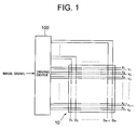
- Fig. 1 shows in summary the configuration of a plasma display device equipped with such a plasma display panel.
- the plasma display panel PDP 10 comprises m column electrodes D 1 to D m , as data electrodes, and n row electrodes X 1 to X n and Y 1 to Y n , arranged to intersect each of the columne elctrodes.
- Each of the pairs X and Y of row electrodes corresponds to a row of the screen.
- These column electrodes D and row electrodes X and Y are formed on two glass substrates, arranged in opposition and enclosing a discharge space into which is injected a discharge gas. At the portions of intersection of each of the row electrodes and column electrodes, discharge cells serving as display elements corresponding to individual pixels are formed.
- discharge cells utilize a discharge phenomenon, they have only two states, "emitting” and “non-emitting”. That is, discharge cells are capable of representing only the brightnesses of two grayscales, at the minimum brightness (the non-emitting state) and at the maximum brightness (the emitting state).
- the driving device 100 executes grayscale driving of the above PDP 10, in which such discharge cells are arranged in a matrix shape, using a subfield method in which intermediate grayscale brightnesses corresponding to input image signals are represented.
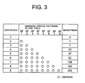
- the display interval for one subfield is divided into, for example, eight subfields SF1 to SF8, as shown in Fig. 2.
- To each of these subfields SF1 to SF8 is allocated a number of times emission is to be executed within that subfield.
- emission is executed, within the display interval of one field, a number of times corresponding to the brightness level of the input image signal.
- an intermediate brightness is perceived corresponding to the total number of emissions executed within the field display interval in question.
- Fig. 3 is a figure showing one example of emission driving patterns, indicating combinations of subfields for which emission is executed and subfields for which emission is not executed.
- the driving device 100 selects one emission driving pattern from among the nine types shown in Fig. 3, according to the input image signal.
- the different driving pulses are applied to the column electrodes D and row electrodes X and Y of the PDP 10 so as to execute emission for the number of times shown in Fig. 2 only in those subfields indicated by white circles in the selected emission driving pattern.
- images can be displayed having nine intermediate brightnesses, with emission brightness ratios of 0, 1, 7, 23, 47, 82, 128, 185, and 255.
- emission driving patterns shown in Fig. 3 after first putting a discharge cell in the non-emitting state in one subfield within a field interval, emission is not executed again in subsequent subfields. That is, as indicated by the white circles, emission driving patterns wherein subfields in which emission is executed continuously (hereafter called the “continuous emission state”) and subfields in which the extinguished state is continuous (hereafter called the “continuous extinguished state”) alternate within a single field interval are excluded.
- the continuous emission state subfields in which emission is executed continuously
- the continuous extinguished state subfields in which the extinguished state is continuous
- the frequency of switching between the above continuous emission state and the above continuous extinguished state is equal to the vertical sync frequency which determines the display interval for a single field.
- the present invention was devised in consideration of this problem, and has as an object the provision of a display panel driving method which is capable of image display with false contours suppressed, without the occurrence of flicker even when the vertical sync frequency of the input image signal is low.
- the display panel driving method of this invention is a method for driving a display panel in which, in a display panel which forms a display screen by means of a plurality of emission elements, each of the above emission elements is driven to emit light in each of N subfields constituting one field interval of an input image signal.
- a first emission driving sequence is executed, in which intermediate brightnesses are represented for each of N+1 gradations, from the first grayscale to the (N+1)th grayscale, by causing the above emission elements to emit in n (where n is an integer from 0 to N) of the above subfields which are continuous within the above one field interval, corresponding to the brightness level represented by the above input image signal; or, a second emission driving sequence is executed, in which intermediate brightnesses are represented for each of N+1 gradations, from the first grayscale to the (N+1)th grayscale, by causing the above emission elements to emit during the first half of the above field period in each of the above subfields which are continuous, corresponding to the brightness level represented by the above input image signal, and then, in the second half of the field period, causing the above emission elements to emit in each of the above subfields which are continuous, corresponding to the brightness level represented by the above input image signal
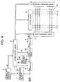
- Fig. 4 is a figure showing the configuration of a plasma display device which drives a plasma display panel according to a driving method of this invention.
- this plasma display device comprises a plasma display panel PDP 10, and driving circuitry, comprising functional modules as described below.
- the driving circuitry comprises a synchronization detection circuit 1; driving control circuit 2; vertical sync frequency detection circuit 3; A/D converter 4; memory 5; address driver 6; first sustaining driver 7; second sustaining driver 8; data conversion circuit 30; and mean brightness detection circuit 40.
- the PDP 10 comprises m column electrodes D 1 to D m as address electrodes, and n each row electrodes X 1 to X n and Y 1 to Y n arranged to intersect each of the column electrodes.
- row electrodes corresponding to one row in the PDP 10 are formed by one pair of the row electrodes X and Y.
- the column electrodes D and the row electrodes X and Y are formed on two glass substrates, arranged in opposition and enclosing a discharge space into which is injected a discharge gas.
- Discharge cells serving as display elements corresponding to individual pixels, are formed at the portions of intersection of each of the row electrode pairs with the column electrodes.
- the synchronization detection circuit 1 When the synchronization detection circuit 1 detects a vertical sync signal in the input image signal, it generates a vertical synchronization detection signal V and supplies this signal to the driving control circuit 2 and the vertical sync frequency detection circuit 3. Also, when the synchronization detection circuit 1 detects a horizontal sync signal in the above input image signal, it generates a horizontal synchronization detection signal H and supplies this signal to the driving control circuit 2.
- the vertical sync frequency detection circuit 3 measures the period of the above vertical synchronization detection signal V, and by this means determines the vertical sync frequency in the above input image signal, and supplies to the driving control circuit 2 and data conversion circuit 30 a vertical sync frequency signal VG which indicates this frequency value.
- the A/D converter 4 samples the above input image signal, according to a clock signal provided by the driving control circuit 2, and converts this into pixel data D with, for example, 8 bits per pixel; this is supplied to the data conversion circuit 30 and the mean brightness detection circuit 40.
- the mean brightness detection circuit 40 determines the mean brightness lever of the input image signal based on the above pixel data D, supplied in order by the A/D converter 4, and supplies a mean brightness signal AB indicating this mean brightness level to the driving control circuit 2.
- the data conversion circuit 30 executes multi-grayscale processing on the above pixel data D, and within one field interval, converts the results into pixel driving data GD to drive the emission of individual discharge cells.
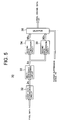
- Fig. 5 is a figure showing the internal configuration of the data conversion circuit 30.
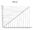
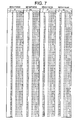
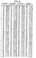
- the first data conversion circuit 32 provides the results of conversion of the above pixel data D into (14x16)/255, based on conversion characteristics as shown in Fig. 6, to the multi-grayscale processing circuit 33 as converted pixel data D H . That is, the first data conversion circuit 32 converts pixel data D, capable of representing the brightnesses of 256 grayscales from 0 to 255 in 8 bits, into converted pixel data D H capable of representing the brightnesses of 225 grayscales from 0 to 224 in 8 bits. Specifically, the first data conversion circuit 32 converts the above pixel data D into converted pixel data D H , based on the conversion tables in Fig. 7 and Fig. 8, which conform to the conversion characteristic shown in Fig. 6.
- the conversion characteristic is set according to the number of bits of the pixel data, the number of compressed bits resulting from conversion to multiple grayscales, described below, and the number of display grayscales.
- conversion is performed by the first data conversion circuit 32, taking into account the number of display grayscales and the number of compressed bits resulting from multi-grayscale processing.
- the occurrence of brightness saturation in the multi-grayscale processing described below, and the occurrence of flat portions in the display characteristic that is, the occurrence of grayscale distortion
- Fig. 9 is a figure showing the internal configuration of the multi-grayscale processing circuit 33, which executes multi-grayscale processing.
- the multi-grayscale processing circuit 33 comprises an error diffusion processing circuit 330 and dither processing circuit 350.
- the data separation circuit 331 in the error diffusion processing circuit 330 separates the lower 2 bits of the 8 bits of converted pixel data D H provided by the above first data conversion circuit 32 as error data, and the upper 6 bits as display data.
- the adder 332 adds this error data, delay output from the delay circuit 334, and multiplication output from the coefficient multiplier 335, and provides the result of addition to the delay circuit 336.
- the delay circuit 336 supplies the addition result from the adder 332, delayed by the time duration of one clock period of pixel data (hereafter called delay time D), to the above coefficient multiplier 335 and delay circuit 337 as the delayed addition signal AD 1 .
- the coefficient multiplier 335 supplies to the above adder 332 the result of multiplying the above delayed addition signal AD 1 by a prescribed coefficient K 1 (for example, "7/16").
- the delay circuit 337 supplies to the delay circuit 338 the above delayed addition signal AD 1 , further delayed by an amount of time (1 horizontal scan interval - above delay time D x 4), as the delayed addition signal AD 2 .
- the delay circuit 338 supplies to the coefficient multiplier 339 this delayed addition signal AD 2 , further delayed by the above delay time D, as the delayed addition signal AD 3 .
- the delay circuit 338 also supplies to the coefficient multiplier 340 the above delayed addition signal AD 2 , delayed by an amount of time (delay time D x 2), as the delayed addition signal AD 4 .
- the delay circuit 338 supplies to the coefficient multiplier 341 the above delayed addition signal AD 2 , delayed by an amount of time (delay time D x 3), as the delayed addition signal AD 5 .
- the coefficient multiplier 339 supplies to the adder 342 the result of multiplying the above delayed addition signal AD 3 by a prescribed coefficient K 2 (for example, "3/16").
- the coefficient multiplier 340 supplies to the adder 342 the result of multiplying the above delayed addition signal AD 4 by a prescribed coefficient K 3 (for example, "5/16").
- the coefficient multiplier 341 supplies to the adder 342 the result of multiplying the above delayed addition signal AD 5 by a prescribed coefficient K 4 (for example, "1/16").
- the adder 342 supplies to the above delay circuit 334 the addition signal obtained by adding the multiplication results supplied by the above coefficient multipliers 339, 340 and 341.
- the delay circuit 334 supplies the addition signal, delayed by an amount of time equal to the above delay time D, to the above adder 332.
- the adder 332 supplies to the adder 333 the above error data, the delayed output from the delay circuit 334, and a carry-out signal C o which is at logical level "0" if there is no carry digit when adding with the multiplication output of the coefficient multiplier 335, and is at logical level "1" if there is a carry digit.
- the adder 333 outputs the result of addition of the above carry-out signal C o to the display data which is the upper 6 bits of the above converted pixel data D H as 6 bits of error diffusion processed pixel data ED.
- prescribed coefficients K 1 to K 4 as described above are used to weight by addition the error data corresponding to the pixel G(j,k-1) on the left of the pixel G(j,k) in question; the pixel G(j-1,k-1) on the upper left; the pixel G(j-1,k) directly above; and the pixel G(j-1,k+1) on the upper right, as follows:
- the upper 6 bits of the converted pixel data D H is taken to be the display data and the remaining lower 2 bits to be the error data, and the weighted error data for each of the peripheral pixels ⁇ G(j,k-1), G(j-1,k+1), G(j-1,k), G(j-1,k-1) ⁇ is reflected in the above display data.
- the brightness of the lower 2 bits at the origin pixel ⁇ G(j,k) ⁇ is approximately represented by the above peripheral pixels, and consequently, 6 bits' worth of display data, fewer than 8 bits' worth, can be used to represent brightness grayscales equivalent to 8 bits' worth of pixel data.
- the dither processing circuit 350 performs dither processing of error diffusion processed pixel data ED supplied by the error diffusion processing circuit 330.
- one intermediate display level is represented by a plurality of neighboring pixels. For example, when the upper 6 bits of pixel data among 8 bits of pixel data are used for grayscale representation equivalent to 8 bits, the four pixels adjacent on the left and right, and above and below, are taken to be one set, and four dither coefficients a to d, which are different coefficient values, are allocated and added to each of the pixel data values corresponding to each of the pixels of this set. Through this dither processing, four pixels can produce combinations of four different intermediate display levels. Hence even if there are only 6 bits of pixel data, the number of levels of brightness grayscales which can be represented is increased fourfold, that is, intermediate grayscales equivalent to 8 bits can be displayed.
- the dither coefficients a to d to be allocated to each of the four pixels are changed for each field.
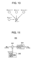
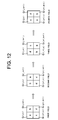
- Fig. 11 is a figure showing the internal configuration of the dither processing circuit 350.
- the dither coefficient generation circuit 352 generates four dither coefficients a, b, c, d for each of four adjacent pixels [G(j,k), G(j,k+1), G(j+1,k), G(j+1,k+1)] as shown in Fig. 12, and supplies these in order to the adder 351. Further, the dither coefficient generation circuit 352 changes, for each field, the allocation of the dither coefficients a through d generated corresponding to each of the four pixels, as shown in Fig. 12.
- dither coefficients a through d are generated in cyclic repetition and supplied to the adder 351, with the following allocations.
- pixel G(j,k) dither coefficient a pixel G(j,k+1): dither coefficient b pixel G(j+1,k): dither coefficient c pixel G(j+1,k+1): dither coefficient d
- pixel G(j,k) dither coefficient b pixel G(j,k+1): dither coefficient a pixel G(j+1,k): dither coefficient d pixel G(j+1,k+1): dither coefficient c
- pixel G(j,k) dither coefficient d pixel G(j,k+1): dither coefficient c pixel G(j+1,k): dither coefficient b pixel G(j+1,k+1): dither coefficient a
- the dither coefficient generation circuit 352 repeatedly executes the operation for the first through fourth fields as described above. That is, after completing the operation to generate dither coefficients in the fourth field, the circuit returns to the operation for the above first field, and repeats the operation described above.
- the adder 351 adds the dither coefficients a through d allocated for each field as described above to the error diffusion processed pixel data ED corresponding to the above pixel G(j,k), pixel G(j,k+1), pixel G(j+1,k), and pixel G(j+1,k+1), supplied from the above error diffusion processing circuit 330.
- the dither added pixel data obtained is supplied to the upper bit extraction circuit 353.
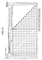
- the second data conversion circuit 34 converts the multi-grayscale pixel data D S into 14-bit pixel driving data GD a according to the data conversion table shown in Fig. 13, and supplies this to the selector 36.
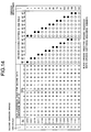
- the second data conversion circuit 35 converts the above multi-grayscale pixel data D S into 14-bit pixel driving data GD b according to the data conversion table shown in Fig. 14, and supplies the result to the selector 36.
- the selector 36 selects GD a from among the above pixel driving data GD a and GD b for use as pixel driving data GD, and supplies this to the memory 5 shown in Fig. 4.
- the selector 36 selects the above pixel driving data GD b , and supplies this to the memory 5 as pixel driving data GD.
- the memory 5 writes in order this pixel driving data GD, according to write signals supplied from the driving control circuit 2.
- the memory 5 reads out the written data according to read signals supplied from the driving control circuit 2. That is, in the memory 5, one screen' s worth of the written pixel driving data GD 11 to GD nm is taken to be pixel driving data bit groups DB1 to DB14, grouped by the bit digit (from the first to the 14th bit).
- the pixel driving data bit groups DB1 to DB14 are as follows.
- the memory 5 reads out in order, one display line at a time, each of these pixel driving data bit groups DB1 to DB14, corresponding to each of the subfields SF1 to SF14 described below.
- the driving control circuit 2 executes emission driving control as follows, according to the above vertical sync frequency signal VF and mean brightness signal AB.
- the driving control circuit 2 When the vertical sync frequency indicated by the above vertical sync frequency signal VF is equal to or greater than, for example, 60 Hz, or when the mean brightness level indicated by the mean brightness signal AB is lower than a prescribed level, the driving control circuit 2 first supplies a logical level "0" flicker suppression signal FS to the data conversion circuit 30. In this process, the selector 36 of the data conversion circuit 30 supplies pixel driving data GD a , converted by the second data conversion circuit 34, to memory 5 in response to this logical level "0" flicker suppression signal FS. The driving control circuit 2 then supplies, to the address driver 6, first sustaining driver 7 and second sustaining driver 8, various timing signals so as to cause emission driving of the PDP 10 according to the emission driving format shown in Fig. 15.
- emission driving is executed as shown in Fig. 13 and Fig. 15.
- the driving control circuit 2 first supplies a logical level "1" flicker suppression signal FS to the data conversion circuit 30.
- the selector 36 of the data conversion circuit 30 supplies to the memory 5 pixel driving data GD b converted by the second data conversion circuit 35 in response to this logical level "1" flicker suppression signal FS.
- the driving control circuit 2 then supplies, to the address driver 6, first sustaining driver 7 and second sustaining driver 8, various timing signals so as to cause emission driving of the PDP 10, according to the emission driving format shown in Fig. 16.
- emission driving is executed as shown in Fig. 14 and Fig. 16.
- the display interval of one field (hereafter this expression also refers to one frame) is divided into 14 subfields SF1 to SF14.
- executed are an address sequence Wc, in which each of the discharge cells of the PDP 10 is set to either the "lit discharge cell state" or the "extinguished discharge cell state", and an emission sustain sequence Ic which causes only discharge cells in the above "lit discharge cell state” to emit repeatedly the number of times indicated in Fig. 15 (or in Fig. 16).
- a simultaneous reset sequence Rc is executed which initializes the wall charge within all the discharge cells of the PDP 10; and in the final subfield SF14, an erasing sequence E is executed which simultaneously eliminates the wall charge within all the discharge cells.
- the emission driving in the subfields SF1, SF3, SF5, SF7, SF9, SF11, SF13 in the emission driving format of Fig. 15 is executed in the first half of the one-field display interval, and the emission driving in the subfields SF2, SF4, SF6, SF8, SF10, SF12, SF14 is executed in the second half.
- the above erasing sequence E is executed in the final subfield SF13 of the first half
- the above simultaneous reset sequence Rc is executed in the leading subfield SF2 of the second half.
- the address driver 6, first sustaining driver 7 and second sustaining driver 8 apply various driving pulses in order to realize the operations of each of the above sequences to the electrodes of the PDP 10, with timing determined by the timing signals supplied by the driving control circuit 2.
- Fig. 17 shows the timing of the application of various driving pulses applied to the column electrodes D and the row electrodes X and Y of the PDP 10 by the above drivers, during the above simultaneous reset sequence Rc, address sequence Wc, emission sustain sequence Ic, and erasing sequence E.
- the first sustaining driver 7 and second sustaining driver 8 each simultaneously apply reset pulses RP X and RP Y to the row electrodes X 1 to X n and Y 1 to Y n , as shown in Fig. 17.
- reset pulses RP X and RP Y In response to the application of these reset pulses RP X and RP Y , all the discharge cells in the PDP 10 undergo reset discharge, and a prescribed uniform wall charge is formed within each of the discharge cells. By this means, all the discharge cells are set to the initial "lit discharge cell state".
- the address driver 6 generates pixel data pulses having voltages corresponding to the logical levels of each pixel driving data bit in the pixel driving data bit group DB read from the above memory 5. For example, the address driver 6 generates a high-voltage pixel data pulse when the logical level of the pixel driving data bit is "1", and generates a low-voltage (0 volt) pixel data pulse when it is "0". The address driver 6 applies these pixel data pulses, one display line (m pulses) at a time, to the column electrodes D 1 to D m . For example, in the address sequence Wc of the subfield SF1, the pixel driving data bit group DB1 is read from memory 5, as described above.
- the address driver 6 first converts m pixel driving data bits corresponding to the first display line in the pixel driving data bit group DB1 into m pixel data pulses having pulse voltages corresponding to the respective logical levels, and applies these to the column electrodes D 1 to D m as the pixel data pulses group DP1.
- the address driver 6 converts the m pixel driving data bits corresponding to the second display line in the pixel driving data bit group DB1 into m pixel data pulses having pulse voltages which correspond to the respective logical levels, and apply these to the column electrodes D 1 to D m as the pixel data pulse group DP2.
- the address sequence Wc of the subfield SF1 is performed to apply pixel data pulse groups DP3 to DPn, corresponding to the 3rd through nth display lines of the pixel data pulse group DP1, in order to the column electrodes D 1 to D m .
- the pixel driving data bit group DB2 is read from memory 5, as described above.
- the address driver 6 converts the m pixel driving data bits corresponding to the first display line in the pixel driving data bit group DB2 into m pixel data pulses having pulse voltages corresponding to the respective logical levels, and applies these to the column electrodes D 1 to D m as the pixel data pulse group DP1.
- the address driver 6 converts the m pixel driving data bits corresponding to the second display line in the pixel driving data bit group DB2 into m pixel data pulses having pulse voltages which correspond to the respective logical levels, and applies these to the column electrodes D 1 to D m as the pixel data pulse group DP2. Subsequently, similar operations are performed in the address sequence Wc of the subfield SF2 to apply pixel data pulse groups DP3 to DPn, corresponding to the 3rd through nth display lines of the pixel data pulse group DP2, in order to the column electrodes D 1 to D m .
- the second sustaining driver 8 in each address sequence Wc the second sustaining driver 8 generates negative-polarity scan pulses SP as shown in Fig. 17, with the same timing as the timing of application of the above-described pixel data pulse groups DP, and applies these in order to the row electrodes Y 1 to Y n .
- discharge selective erasing discharge
- the wall charge which had remained within the discharge cells is then selectively eliminated.
- Discharge cells which have been initialized by this selective erasing discharge to the "lit discharge cell state" in the above simultaneous reset sequence Rc are set to the "extinguished discharge cell state".
- discharge is not induced in discharge cells belonging to column electrodes D to which a low-voltage pixel data pulse is applied, and the current state is maintained. That is, discharge cells in the "extinguished discharge cell state” remain in the “extinguished discharge cell state", and discharge cells in the "lit discharge cell state” are maintained in the "lit discharge cell state".
- positive-polarity sustain pulses IP X and IP Y are applied repeatedly in alternation to the row electrodes X 1 to X n and Y 1 to Y n by the first sustaining driver 7 and second sustaining driver 8, as shown in Fig. 17. As shown in Figs.
- the number of times that the above sustain pulse IP is applied repeatedly is, if the number of times in SF1 is "1": SF1 1 SF2 3 SF3 5 SF4 8 SF5 10 SF6 13 SF7 16 SF8 19 SF9 22 SF10 25 SF11 28 SF12 32 SF13 35 SF14 39
- the second sustaining driver 8 In the erasing sequence E, the second sustaining driver 8 generates negative-polarity erasing pulses EP and applies them to the row electrodes Y 1 through Y n , as shown in Fig. 17. Through application of these erasing pulses EP, an erasing discharge is induced within all the discharge cells of the PDP 10, and the wall charge remaining within all the discharge cells is annihilated. That is, by means of this erasing discharge, all the discharge cells in the PDP 10 are forcibly set to the "extinguished discharge cell state".
- each discharge cell is set to the "lit discharge cell state” or to the "extinguished discharge cell state” is determined by the pixel driving data GD a or GD b shown in Fig. 13 or Fig. 14. That is, if a bit in the pixel driving data GD is at logical level "1", selective erasing discharge is induced in the address sequence Wc of the subfield corresponding to the bit digit, and the discharge cell is put into the "extinguished discharge cell state". On the other hand, if a bit in the pixel driving data GD is at logical level "0”, then the above selective erasing discharge is not induced in the address sequence Wc of the subfield corresponding to the bit digit. Hence discharge cells in the "extinguished discharge cell state" remain in the "extinguished discharge cell state", and discharge cells in the "lit discharge cell state” are maintained in the "lit discharge cell state".
- each of the first through 14th bits determines whether or not selective erasing discharge is induced in the address sequence Wc for the respective subfields SF1 to SF14 in Fig. 15.
- the pixel driving data GD a shown in Fig. 13 is used to perform driving according to the emission driving format of Fig. 15, first all the discharge cells are initialized to the "lit discharge cell state" in subfield SF1. The "lit discharge cell state" of discharge cells is maintained until a selective erasing discharge is induced by the address sequence Wc in the subfields indicated by black circles in Fig. 13.
- the first through 14th bits correspond to the subfields SF1 to SF14 in Fig. 16 as follows.
- the simultaneous reset sequence Rc is executed in subfield SF2 as well as in subfield SF1.
- the 15 patterns of pixel driving data GD b are used to perform driving according to the emission driving format shown in Fig. 16, similarly to the driving shown in Figs. 13 and 15 and described above, it is possible to express intermediate-level brightnesses in 15 stages: ⁇ 0:1:4:9:17:27:40:56:75:97:122:150:182:217:255 ⁇
- grayscale driving is adopted in which the display interval for one field is divided into first-half driving intervals (SF1, SF3, SF5, SF7, SF9, SF11, SF13) and second-half driving intervals (SF2, SF4, SF6, SF8, SF10, SF12, SF14).
- first-half driving intervals SF1, SF3, SF5, SF7, SF9, SF11, SF13
- second-half driving intervals SF2, SF4, SF6, SF8, SF10, SF12, SF14
- the time between the moment of initiation of emission in the above first-half driving interval, and the moment of initiation of emission in the second-half driving interval is approximately 1/2 the display interval for one field, and the frequency of switching between the above continuous emission state and the above continuous extinguished state is approximately 2 times the vertical sync frequency which determines the display interval for one field.
- the first emission driving (Fig. 13 and Fig. 15), in which discharge cells are caused to emit in each of a number of continuous subfields corresponding to the brightness level of the input image signal within one field.
- this first emission driving there exist no emission driving patterns in which continuous emission intervals and continuous extinguished intervals are inverted within one field display interval, so that the occurrence of false contours is suppressed.
- reset discharge which incurs comparatively large power consumption, is executed only once, at the beginning of the field, so that power consumption can be suppressed.
- the second emission driving (Fig. 14 and Fig. 16) is executed, in which, in each of the first and second halves of one field, discharge cells are caused to emit in a number of continuous subfields corresponding to the brightness level of the input image signal.
- this second emission discharge there exist no emission discharge patterns within one field display interval such that continuous emission intervals and continuous extinguished intervals are inverted, so that the occurrence of false contours is suppressed.
- the number of times within one field display interval that there is switching from the continuous emission state to the continuous extinguished state is at most 2 times.
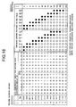
- the conversion table used by the second data conversion circuit 35 that shown in Fig. 18 may be adopted in place of the table of Fig. 14, in order to reliably induce this selective erasing discharge.
- pixel driving data GD b converted using this conversion table selective erasing discharge is induced in each of two continuous subfields, as indicated by the black circles in Fig. 18. Consequently, even if the wall charge within a discharge cell cannot be properly annihilated by the first selective erasing discharge, the wall charge can be annihilated normally through the second selective erasing discharge.
- the subfields SF1, SF3, SF5, SF7, SF9, SF11, SF13 are executed in the first half of a field, and the subfields SF2, SF4, SF6, SF8, SF10, SF12, SF14 are executed in the second half; but other methods are possible.
- Fig. 19 is a figure showing a modified example of the emission driving format shown in Fig. 16, in consideration of this point.
- the subfields SF1, SF4, SF5, SF8, SF9, SF12, SF13 are executed in order in the first half of a field, and in the second half, SF2, SF3, SF6, SF7, SF10, SF11, SF14 are executed in order.
- Fig. 20 is a figure showing the data conversion table used in the second data conversion circuit 34 when executing emission driving control adopting the emission driving format shown in Fig. 19, and an emission driving pattern.
- the first through 14th bits of the pixel driving data GD b shown in Fig. 20 are associated with the subfields SF1 to SF14 shown in Fig. 19 as follows.
- the so-called selective erasing address method was adopted in which all the discharge cells are initialized to the "lit discharge cell state" in advance, and the wall charge is eliminated selectively according to the pixel data to set the "extinguished discharge cell state".
- Fig. 21 is a figure showing an emission driving format during the first emission driving, used when adopting this selected writing address method
- Fig. 22 shows an emission driving format during the second emission driving
- Fig. 23 is a figure showing the data conversion table used in the second data conversion circuit 34 when adopting the emission driving format shown in Fig. 21, and the emission driving pattern
- Fig. 24 shows the data conversion table used by the second data conversion circuit 35 when adopting the emission driving format shown in Fig. 22, and the emission driving pattern.
- grayscale driving is executed in order from subfield SF14 to SF1.
- a simultaneous reset sequence Rc' in which the wall charge remaining in all discharge cells is eliminated simultaneously to initialize all discharge cells to the "extinguished discharge cell state" is executed only in the leading subfield SF14.
- an address sequence Wc' and an emission sustain sequence Ic are executed.
- selected write discharge to form wall charge is induced only in the address sequences Wc' of subfields (indicated by black circles) corresponding to the digits of bits with a logical level "1" in the pixel driving data GD shown in Fig. 23.
- Discharge cells in which this selected writing discharge is induced are set to the "lit discharge cell state".
- emission is executed in the emission sustain sequences Ic for subfields indicated by black or white circles in Fig. 23 only a number of times corresponding to the weighting of each subfield.
- the number of switches from the continuous emission state, in which subfields of sustaining discharge emission (indicated by black or white circles in Fig. 23) are continuous, to the continuous extinguished state in which subfields in the extinguished state are continuous is at most one.
- the subfields SF13, SF11, SF9, SF7, SF5, SF3, SF1 are executed in order in the first half of one field, and SF14, SF12, SF10, SF8, SF6, SF4, SF2 are executed in order in the second half.
- the simultaneous reset sequence Rc is executed, similarly to the case described above, in the leading subfield of the first half SF13 and in the leading subfield of the second half SF14.
- the above-described address sequence Wc' and emission sustain sequence Ic are executed. In this process, the first through 14th bits of the pixel driving data GD b shown in Fig.
- emission is performed the number of times corresponding to the weighting of subfields indicated by black and white circles in Fig. 24 only in the emission sustain sequence Ic.
- switching from the continuous extinguished state to the continuous emission state is performed at most two times during the display interval for one field, similarly to the emission driving shown in Fig. 14.
- the driving control circuit 2 executes the first emission driving, shown in Figs. 21 and 23.
- the second emission driving shown in Figs. 22 and 24 is executed, so that switching during the display interval of one field from the continuous extinguished state to the continuous emission state occurs at most two times.
- odd-numbered subfields are executed in the first half of the field, and even-numbered subfields are executed in the second half; but the two may be interposed.
- Fig. 25 is a figure showing an emission driving format in second emission driving, taking this point into consideration.
- the subfields SF2, SF4, SF6, SF8, SF10, SF12, SF14, having ratios of the number of emissions to be performed in each emission sustain sequence Ic equal to [3:8:13:19:25:32:39], are executed in order in the first half of the field.
- the subfields SF1, SF3, SF5, SF7, SF9, SF11, SF13, having ratios of the number of emissions to be performed in each emission sustain sequence Ic equal to [1:5:10:16:22:28:35] are executed in order.
- Fig. 26 is a figure showing the data conversion table used in the second data conversion circuit 35 when adopting the emission driving format shown in Fig. 25, and the emission driving pattern.
- the first through 14th bits of the pixel driving data GD b shown in Fig. 26 are associated with the subfields SF1 to SF14 shown in Fig. 25 as follows.
- the subfield series of the first half of the field in the second emission driving shown in Figs. 14 and 16 (SF1, SF3, SF5, SF7, SF9, SF11, SF13) and the subfield series of the second half (SF2, SF4, SF6, SF8, SF10, SF12, SF14) are inverted.
- the subfield series of the first half of the field in the second emission driving shown in Figs. 22 and 24 (SF13, SF11, SF9, SF7, SF5, SF3, SF1) and the subfield series of the second half (SF14, SF12, SF10, SF8, SF6, SF4, SF2) are inverted.
- one field is divided into an even number (14) of subfields to perform grayscale driving of the PDP 10; but the number of subfields into which the field is divided is not limited to an even number.
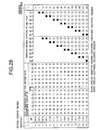
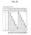
- Fig. 29 and Fig. 30 are figures showing an example of the emission driving pattern in second emission driving adopted when one field is divided into an odd number (13) of subfields to drive the PDP 10.
- Fig. 29 and Fig. 30 show the emission driving patterns in second emission driving when adopting the selective erasing address method and the selected writing address method, respectively.
- subfields SF1, SF3, SF5, SF7, SF9, SF11, SF13, having a ratio of the number of times emission is to be executed in each emission sustain sequence Ic equal to [1:5:10:16:22:28:35] are executed in order in the first half of the field.
- subfields SF2, SF4, SF6, SF8, SF10, SF12, having a ratio of the number of times emission is to be executed in each emission sustain sequence Ic equal to [3:8:13:19:25:32], are executed in order.
- subfields SF13, SF11, SF9, SF7, SF5, SF3, SF1 having a ratio of the number of times emission is to be executed in each emission sustain sequence Ic equal to [35:28:22:16:10:5:1] are executed in order in the first half of the field.
- subfields SF12, SF10, SF8, SF6, SF4, SF2 having a ratio of the number of times emission is to be executed in each emission sustain sequence Ic equal to [32:25:19:13:8:3], are executed in order.
- emission elements comprised by pixels are caused to emit in a number of continuous subfields within one field corresponding to the brightness level expressed by the input image signal.
- emission elements are caused to emit in each of a number of continuous subfields, in the first half and in the second half of a field, according to the brightness level expressed by the image signal.
- the number of times there is switching from the continuous emission state to the continuous extinguished state within the display interval for one field is two times.
Landscapes
- Engineering & Computer Science (AREA)
- Physics & Mathematics (AREA)
- Computer Hardware Design (AREA)
- General Physics & Mathematics (AREA)
- Theoretical Computer Science (AREA)
- Power Engineering (AREA)
- Plasma & Fusion (AREA)
- Control Of Indicators Other Than Cathode Ray Tubes (AREA)
- Control Of Gas Discharge Display Tubes (AREA)
- Transforming Electric Information Into Light Information (AREA)
Applications Claiming Priority (2)
| Application Number | Priority Date | Filing Date | Title |
|---|---|---|---|
| JP2001181109 | 2001-06-15 | ||
| JP2001181109A JP4703892B2 (ja) | 2001-06-15 | 2001-06-15 | ディスプレイパネルの駆動方法 |
Publications (2)
| Publication Number | Publication Date |
|---|---|
| EP1267321A2 true EP1267321A2 (de) | 2002-12-18 |
| EP1267321A3 EP1267321A3 (de) | 2008-02-27 |
Family
ID=19021427
Family Applications (1)
| Application Number | Title | Priority Date | Filing Date |
|---|---|---|---|
| EP02011642A Withdrawn EP1267321A3 (de) | 2001-06-15 | 2002-05-29 | Anzeigetafel und Verfahren zur Steuerung derselben |
Country Status (3)
| Country | Link |
|---|---|
| US (1) | US6982732B2 (de) |
| EP (1) | EP1267321A3 (de) |
| JP (1) | JP4703892B2 (de) |
Cited By (3)
| Publication number | Priority date | Publication date | Assignee | Title |
|---|---|---|---|---|
| EP1587053A3 (de) * | 2004-04-14 | 2007-07-18 | LG Electronics Inc. | Plasma-Anzeigegerät und Bildverarbeitungsverfahren dafür |
| EP1763007A3 (de) * | 2005-09-07 | 2007-10-17 | Pioneer Corporation | Ansteuerverfahren für eine Anzeigetafel |
| EP1496493A3 (de) * | 2003-07-07 | 2008-04-02 | Pioneer Corporation | Verfahren zum Steuern einer Anzeigetafel |
Families Citing this family (7)
| Publication number | Priority date | Publication date | Assignee | Title |
|---|---|---|---|---|
| EP1554714B1 (de) * | 2002-10-16 | 2006-03-29 | Koninklijke Philips Electronics N.V. | Anzeigevorrichtung mit einer anzeigeeinrichtung und verfahren zur ansteuerung der anzeigeeinrichtung |
| JP4559041B2 (ja) * | 2003-06-12 | 2010-10-06 | パナソニック株式会社 | 多階調画像表示装置及びその動画偽輪郭低減方法 |
| GB0319963D0 (en) * | 2003-08-27 | 2003-09-24 | Koninkl Philips Electronics Nv | Display device |
| KR100497234B1 (ko) | 2003-10-01 | 2005-06-23 | 삼성에스디아이 주식회사 | 플라즈마 디스플레이 패널의 화상 표시 방법 및 그 장치 |
| KR101422006B1 (ko) * | 2007-09-17 | 2014-07-23 | 엘지전자 주식회사 | 데이터의 인코딩/디코딩 방법, 데이터의 검출방법 및데이터의 기록/재생 방법 |
| KR20130087927A (ko) * | 2012-01-30 | 2013-08-07 | 삼성디스플레이 주식회사 | 영상 신호 처리 장치 및 영상 신호 처리 방법 |
| CN107038993B (zh) * | 2017-05-23 | 2019-07-16 | 西安诺瓦电子科技有限公司 | 参数调节方法及装置、显示系统 |
Family Cites Families (13)
| Publication number | Priority date | Publication date | Assignee | Title |
|---|---|---|---|---|
| JP3489884B2 (ja) * | 1994-02-08 | 2004-01-26 | 富士通株式会社 | フレーム内時分割型表示装置及びフレーム内時分割型表示装置における中間調表示方法 |
| US5818419A (en) * | 1995-10-31 | 1998-10-06 | Fujitsu Limited | Display device and method for driving the same |
| JP3408680B2 (ja) * | 1995-10-31 | 2003-05-19 | 富士通株式会社 | 表示装置及びその駆動方法 |
| JP3375473B2 (ja) * | 1995-10-31 | 2003-02-10 | 富士通株式会社 | 表示装置及びその駆動方法 |
| WO1998039762A1 (en) * | 1997-03-07 | 1998-09-11 | Koninklijke Philips Electronics N.V. | A circuit for and method of driving a flat panel display in a sub field mode and a flat panel display with such a circuit |
| JP3703247B2 (ja) * | 1997-03-31 | 2005-10-05 | 三菱電機株式会社 | プラズマディスプレイ装置及びプラズマディスプレイ駆動方法 |
| JP2994630B2 (ja) * | 1997-12-10 | 1999-12-27 | 松下電器産業株式会社 | 明るさによるサブフィールド数調整可能な表示装置 |
| EP0982707A1 (de) * | 1998-08-19 | 2000-03-01 | Deutsche Thomson-Brandt Gmbh | Verfahren und Vorrichtung zur Verarbeitung von Videobildern, insbesondere zur Reduzierung grossflächigen Flimmereffekts |
| EP0982708B1 (de) * | 1998-08-19 | 2011-05-11 | Thomson Licensing | Verfahren und Vorrichtung zur Verarbeitung von Videobildern, insbesondere zur Reduzierung von grossflächigem Flimmereffekt |
| EP1020838A1 (de) * | 1998-12-25 | 2000-07-19 | Pioneer Corporation | Verfahren zur Ansteuerung einer Plasmaanzeigetafel |
| EP1022714A3 (de) * | 1999-01-18 | 2001-05-09 | Pioneer Corporation | Verfahren zur Ansteuerung einer Plasmaanzeigetafel |
| JP3741417B2 (ja) * | 2000-04-18 | 2006-02-01 | パイオニア株式会社 | ディスプレイパネルの駆動方法 |
| JP2002229510A (ja) * | 2000-12-05 | 2002-08-16 | Lg Electronics Inc | プラズマディスプレーパネルの最適の発光パターン生成方法と輪郭ノイズ測定方法及びグレースケール選択方法 |
-
2001
- 2001-06-15 JP JP2001181109A patent/JP4703892B2/ja not_active Expired - Fee Related
-
2002
- 2002-05-29 EP EP02011642A patent/EP1267321A3/de not_active Withdrawn
- 2002-06-07 US US10/163,593 patent/US6982732B2/en not_active Expired - Fee Related
Cited By (3)
| Publication number | Priority date | Publication date | Assignee | Title |
|---|---|---|---|---|
| EP1496493A3 (de) * | 2003-07-07 | 2008-04-02 | Pioneer Corporation | Verfahren zum Steuern einer Anzeigetafel |
| EP1587053A3 (de) * | 2004-04-14 | 2007-07-18 | LG Electronics Inc. | Plasma-Anzeigegerät und Bildverarbeitungsverfahren dafür |
| EP1763007A3 (de) * | 2005-09-07 | 2007-10-17 | Pioneer Corporation | Ansteuerverfahren für eine Anzeigetafel |
Also Published As
| Publication number | Publication date |
|---|---|
| US20030112256A1 (en) | 2003-06-19 |
| JP2002372947A (ja) | 2002-12-26 |
| US6982732B2 (en) | 2006-01-03 |
| EP1267321A3 (de) | 2008-02-27 |
| JP4703892B2 (ja) | 2011-06-15 |
Similar Documents
| Publication | Publication Date | Title |
|---|---|---|
| JP3730826B2 (ja) | プラズマディスプレイパネルの駆動方法 | |
| JPH1173157A (ja) | ディスプレイパネルの中間調表示方法 | |
| JP2003015588A (ja) | ディスプレイ装置 | |
| JP4253422B2 (ja) | プラズマディスプレイパネルの駆動方法 | |
| JP2002023693A (ja) | プラズマディスプレイパネルの駆動方法 | |
| JP4410997B2 (ja) | 表示パネルの駆動装置 | |
| JP2001337648A (ja) | プラズマディスプレイパネルの駆動方法 | |
| JP3961171B2 (ja) | ディスプレイ装置の多階調処理回路 | |
| JP3761132B2 (ja) | ディスプレイパネルの駆動方法 | |
| JP2001312244A (ja) | プラズマディスプレイパネルの駆動方法 | |
| JP3678401B2 (ja) | プラズマディスプレイパネルの駆動方法 | |
| JP2000231362A (ja) | プラズマディスプレイパネルの駆動方法 | |
| EP1267321A2 (de) | Anzeigetafel und Verfahren zur Steuerung derselben | |
| JPH09218662A (ja) | 自発光画像表示パネルの駆動方法 | |
| JP2005321442A (ja) | ディスプレイ装置のディザ処理回路 | |
| EP1262943A2 (de) | Verfahren und Einrichtung zum Steuern einer Plasmaanzeigetafel | |
| JP3734244B2 (ja) | ディスプレイパネルの駆動方法 | |
| JP4698076B2 (ja) | プラズマディスプレイパネルの駆動方法 | |
| JP4071382B2 (ja) | プラズマディスプレイパネルの駆動方法 | |
| JP2003076319A (ja) | プラズマディスプレイパネルの駆動方法 | |
| JP3608713B2 (ja) | プラズマディスプレイパネルの駆動方法 | |
| JP4408350B2 (ja) | 表示パネルの駆動方法 | |
| JP4731738B2 (ja) | 表示装置 | |
| EP1585093A2 (de) | Steuerungsverfahren einer elektrolumineszenten oder Plasmaanzeigetafel | |
| JP3868457B2 (ja) | ディスプレイパネルの駆動方法 |
Legal Events
| Date | Code | Title | Description |
|---|---|---|---|
| PUAI | Public reference made under article 153(3) epc to a published international application that has entered the european phase |
Free format text: ORIGINAL CODE: 0009012 |
|
| AK | Designated contracting states |
Kind code of ref document: A2 Designated state(s): AT BE CH CY DE DK ES FI FR GB GR IE IT LI LU MC NL PT SE TR |
|
| AX | Request for extension of the european patent |
Free format text: AL;LT;LV;MK;RO;SI |
|
| RAP1 | Party data changed (applicant data changed or rights of an application transferred) |
Owner name: PIONEER DISPLAY PRODUCTS CORPORATION Owner name: PIONEER CORPORATION |
|
| PUAL | Search report despatched |
Free format text: ORIGINAL CODE: 0009013 |
|
| AK | Designated contracting states |
Kind code of ref document: A3 Designated state(s): AT BE CH CY DE DK ES FI FR GB GR IE IT LI LU MC NL PT SE TR |
|
| AX | Request for extension of the european patent |
Extension state: AL LT LV MK RO SI |
|
| AKX | Designation fees paid | ||
| STAA | Information on the status of an ep patent application or granted ep patent |
Free format text: STATUS: THE APPLICATION IS DEEMED TO BE WITHDRAWN |
|
| 18D | Application deemed to be withdrawn |
Effective date: 20080828 |
|
| REG | Reference to a national code |
Ref country code: DE Ref legal event code: 8566 |