EP1267318A1 - Filter for displaying, display unit and production method therefor - Google Patents
Filter for displaying, display unit and production method therefor Download PDFInfo
- Publication number
- EP1267318A1 EP1267318A1 EP01949054A EP01949054A EP1267318A1 EP 1267318 A1 EP1267318 A1 EP 1267318A1 EP 01949054 A EP01949054 A EP 01949054A EP 01949054 A EP01949054 A EP 01949054A EP 1267318 A1 EP1267318 A1 EP 1267318A1
- Authority
- EP
- European Patent Office
- Prior art keywords
- transparent
- layer
- electrically conductive
- film
- display
- Prior art date
- Legal status (The legal status is an assumption and is not a legal conclusion. Google has not performed a legal analysis and makes no representation as to the accuracy of the status listed.)
- Withdrawn
Links
Images





Classifications
-
- G—PHYSICS
- G02—OPTICS
- G02B—OPTICAL ELEMENTS, SYSTEMS OR APPARATUS
- G02B5/00—Optical elements other than lenses
- G02B5/20—Filters
-
- G—PHYSICS
- G02—OPTICS
- G02B—OPTICAL ELEMENTS, SYSTEMS OR APPARATUS
- G02B1/00—Optical elements characterised by the material of which they are made; Optical coatings for optical elements
- G02B1/10—Optical coatings produced by application to, or surface treatment of, optical elements
- G02B1/11—Anti-reflection coatings
-
- G—PHYSICS
- G02—OPTICS
- G02B—OPTICAL ELEMENTS, SYSTEMS OR APPARATUS
- G02B1/00—Optical elements characterised by the material of which they are made; Optical coatings for optical elements
- G02B1/10—Optical coatings produced by application to, or surface treatment of, optical elements
- G02B1/11—Anti-reflection coatings
- G02B1/113—Anti-reflection coatings using inorganic layer materials only
- G02B1/115—Multilayers
- G02B1/116—Multilayers including electrically conducting layers
-
- G—PHYSICS
- G02—OPTICS
- G02B—OPTICAL ELEMENTS, SYSTEMS OR APPARATUS
- G02B5/00—Optical elements other than lenses
- G02B5/20—Filters
- G02B5/22—Absorbing filters
- G02B5/223—Absorbing filters containing organic substances, e.g. dyes, inks or pigments
-
- G—PHYSICS
- G02—OPTICS
- G02F—OPTICAL DEVICES OR ARRANGEMENTS FOR THE CONTROL OF LIGHT BY MODIFICATION OF THE OPTICAL PROPERTIES OF THE MEDIA OF THE ELEMENTS INVOLVED THEREIN; NON-LINEAR OPTICS; FREQUENCY-CHANGING OF LIGHT; OPTICAL LOGIC ELEMENTS; OPTICAL ANALOGUE/DIGITAL CONVERTERS
- G02F1/00—Devices or arrangements for the control of the intensity, colour, phase, polarisation or direction of light arriving from an independent light source, e.g. switching, gating or modulating; Non-linear optics
- G02F1/01—Devices or arrangements for the control of the intensity, colour, phase, polarisation or direction of light arriving from an independent light source, e.g. switching, gating or modulating; Non-linear optics for the control of the intensity, phase, polarisation or colour
- G02F1/13—Devices or arrangements for the control of the intensity, colour, phase, polarisation or direction of light arriving from an independent light source, e.g. switching, gating or modulating; Non-linear optics for the control of the intensity, phase, polarisation or colour based on liquid crystals, e.g. single liquid crystal display cells
- G02F1/133—Constructional arrangements; Operation of liquid crystal cells; Circuit arrangements
- G02F1/1333—Constructional arrangements; Manufacturing methods
- G02F1/1335—Structural association of cells with optical devices, e.g. polarisers or reflectors
- G02F1/133502—Antiglare, refractive index matching layers
-
- H—ELECTRICITY
- H05—ELECTRIC TECHNIQUES NOT OTHERWISE PROVIDED FOR
- H05K—PRINTED CIRCUITS; CASINGS OR CONSTRUCTIONAL DETAILS OF ELECTRIC APPARATUS; MANUFACTURE OF ASSEMBLAGES OF ELECTRICAL COMPONENTS
- H05K9/00—Screening of apparatus or components against electric or magnetic fields
- H05K9/0073—Shielding materials
- H05K9/0094—Shielding materials being light-transmitting, e.g. transparent, translucent
- H05K9/0096—Shielding materials being light-transmitting, e.g. transparent, translucent for television displays, e.g. plasma display panel
-
- H—ELECTRICITY
- H01—ELECTRIC ELEMENTS
- H01J—ELECTRIC DISCHARGE TUBES OR DISCHARGE LAMPS
- H01J2211/00—Plasma display panels with alternate current induction of the discharge, e.g. AC-PDPs
- H01J2211/20—Constructional details
- H01J2211/34—Vessels, containers or parts thereof, e.g. substrates
- H01J2211/44—Optical arrangements or shielding arrangements, e.g. filters or lenses
- H01J2211/446—Electromagnetic shielding means; Antistatic means
-
- H—ELECTRICITY
- H01—ELECTRIC ELEMENTS
- H01J—ELECTRIC DISCHARGE TUBES OR DISCHARGE LAMPS
- H01J2329/00—Electron emission display panels, e.g. field emission display panels
- H01J2329/86—Vessels
- H01J2329/89—Optical components structurally combined with the vessel
- H01J2329/892—Anti-reflection, anti-glare, viewing angle and contrast improving means
Definitions
- This invention relates to a display filter which is disposed on a screen of a display such as a plasma display (PDP), a Braun tube (CRT), and a liquid crystal display apparatus (LCD) and which has filter characteristics that are capable of shielding other electromagnetic waves than a visible light from among electromagnetic waves to be generated from the display screen and/or other filter characteristics that are capable of correcting a visible light spectrum, a display apparatus mounted with the filter and a method for production of the same.
- a display filter which is disposed on a screen of a display such as a plasma display (PDP), a Braun tube (CRT), and a liquid crystal display apparatus (LCD) and which has filter characteristics that are capable of shielding other electromagnetic waves than a visible light from among electromagnetic waves to be generated from the display screen and/or other filter characteristics that are capable of correcting a visible light spectrum
- a display has spread wide for use in a television set, a personal computer, or the like, and the display is required for increasing a size thereof as well as decreasing thickness thereof.
- a plasma display has attracted attention as a thin-type display in a large size.
- the plasma display emits an intense leakage electromagnetic field and a near-infrared ray from a display screen.
- the near-infrared ray emitted from the display screen may act on the electronic equipment such as a cordless phone located around the display and cause malfunction thereof.
- near-infrared rays having wavelengths of 820 nm, 880 nm, 980 nm and the like are used in a remote controller and optical communication by a transmission system, it is necessary to suppress light having a wavelength in a range of from 800 to 1100 nm which is in a near-infrared region to such a level as does not cause a problem in practical use.
- a near-infrared absorption filter produced by using a near-infrared absorbing dye is used.
- the near-infrared absorbing dye is liable to be deteriorated by environmental factors such as humidity, heat and light, there is a tendency that the near-infrared absorption filter which uses the dye may undergo changes in optical properties such as decrease in near-infrared ray cutting-off capacity, and a change of a color transmitted through the filter with the lapse of time.
- the plasma display emits the intense near-infrared ray over a wide wavelength range
- a conventional near-infrared absorption filter only a near-infrared absorption filter in which visible light ray transmittance is low has been realized.
- a transparent electrically conductive layer is ordinarily used as such a method and, on this occasion, such transparent electrically conductive layers are broadly classified into 2 categories : an electrically conductive mesh; and a transparent electrically conductive thin film.
- the electrically conductive mesh ordinarily used is a grounded metallic mesh, a synthetic fiber mesh or a metallic fiber mesh which has been coated with a metal, an etched film which has been produced by first forming a metallic film and then performing an etching treatment on the thus-formed film in a lattice pattern manner or the like.
- these electrically conductive mesh are excellent in electromagnetic wave shielding capacity because of high electric conductivity thereof, these electrically conductive mesh have disadvantages that fringes are produced by an interference of light, a low yield causes an increase in cost and the like.
- a transparent electrically conductive thin film comprising a metallic thin film, an oxide semiconductor thin film and the like as an electromagnetic wave shielding layer, instead of using the electric conductive mesh.
- the metallic thin film can obtain favorable electric conductivity, but fails to provide a high visible light ray transmittance owing to reflection and absorption by the metal over a wide wavelength range.
- the oxide semiconductor thin film has higher transparency than that of the metallic thin film, but is inferior in electric conductivity and near-infrared reflectivity.
- the transparent electrically conductive layer for the purpose of cutting-off the leakage electromagnetic field, there are many cases in which, when the shield capacity thereof is regarded as being important, the electrically conductive mesh is used while, when cost performance is regarded as being important, the transparent electrically conductive thin film is used.
- JP-A 58-153904 Japanese Unexamined Patent Publication JP-A 58-153904 (1983), JP-A 60-22102 (1985), or JP-A 59-221943 (1984) and the like.
- An application thereof to a plasma display panel is recited in JP-A 58-153904.
- a plasma display filter is formed separately from the display and, then, disposed as a front surface panel of the display for the purposes of cutting off the near-infrared rays and electromagnetic waves, and protecting the display screen.
- a front surface panel method brings about a cost increase owing to a many number of components and/or production processes of the plasma display filter whereupon it becomes difficult to allow the plasma display filter to be smaller in thickness and lighter in weight.
- reflection on a surface of a representation portion of the plasma display is not ordinarily decreased and reflectance of a glass substrate is maintained; on this occasion, when the front surface panel is disposed apart from the representation portion from a viewpoint of thermal design and the like, a reflected image becomes double-or-more-images caused by reflections of external light on the display surface and the front surface panel whereupon there is a case in which visibility of the display is deteriorated.
- the plasma display has characteristics that, due to reflection of glass or phosphor on the surface of the screen, contrast in a bright place is low as well as a color reproduction gamut of luminescence is narrow.
- the transparent polymer film having various types of functions in application fields according to the present invention is used in roll form and, from the standpoint of operational efficiency and the like, the transparent polymer film having a thickness of from 75 to 100 ⁇ m is used. Therefore, when 2 sheets of the transparent polymer films each having a function are simply bonded with each other, a total thickness merely comes to be less than 0.3mm.
- an anti-reflection film that having a thickness of 188 ⁇ m has been used in some cases and, in these cases, a base film thereof was polyethylene terephthalate (PET); however, since it is inferior in an anti-reflection property to triacetyl cellulose (TAC) in which a favorably used base film is 80 ⁇ m thick, it is not used in a positive manner for the purpose of bonding films with each other.
- PET polyethylene terephthalate
- TAC triacetyl cellulose
- an electromagnetic wave shielding body it is necessary to establish conduction between the transparent electrically conductive layer and an outside by using an electrode which leads the electromagnetic wave out to the outside as an electric current.
- an electrode which leads the electromagnetic wave out to the outside as an electric current.
- the film is bonded such that a portion of the layer is exposed on a periphery of the filter to allow the thus-exposed portion to become a position which performs electric conduction with the outside as an electrode.
- the electromagnetic wave shielding body obtained by bonding the film to the front surface panel has established conduction with the outside by this method.
- an electrode has been disposed on an entire peripheral portion thereof.
- a display filter which has desired filter characteristics such as electromagnetic wave shielding capacity, near-infrared ray cutting-off capacity, and image improvement capacity and which is capable of aiming for improvements such as a low cost, a lighter weight, a smaller thickness, a panel protection, workability when a trouble occurs, and enhancement of productivity, a display apparatus mounted with the filter, and a method for production of the same.
- a transparent electrically conductive layer having a surface resistance of from 0.01 to 30 ⁇ /square is necessary to shield an extremely intense electromagnetic wave emitted from a plasma display; 2) a display apparatus using the plasma display excellent in electromagnetic wave shielding capacity, near-infrared ray cutting-off capacity and an image/visibility/a cost can be obtained by forming an electromagnetic wave shielding body equipped with such a transparent electrically conductive layer directly on a surface of the plasma display; 3) the display apparatus using a display excellent in the image/visibility/the cost can be obtained by forming a light control film which has a specified layer constitution, contains a dye and has visible light ray transmittance of from 30 to 85% directly on the surface of the display; 4) On a basis of attaining lighter weight and smaller thickness as well as panel protectivity, an enhancement of workability can be attained by setting a total thickness of a transparent polymer film which constitutes an optical filter to be 0.3 mm
- the invention provides a display filter capable of being adhered to a display screen and having predetermined filter characteristics, comprising:
- a transparent electrically conductive layer (D) having a surface resistance of from 0.01 to 30 ⁇ /square is disposed between the functional transparent layer (A) and the polymer film (B) and/or between the polymer film (B) and the transparent adhesive layer (C).
- a portion or entirety of the transparent electrically conductive layer (D) is constituted by an electrically conductive mesh.
- the transparent electrically conductive layer (D) is constituted by firstly laminating a repeating unit (Dt)/(Dm) comprising a high-refractive-index transparent thin film layer (Dt) and a metallic thin film layer (Dm) while repeating the repeating unit from 2 times to 4 times and, then, on the resultant laminate, further laminating a high-refractive-index thin film layer (Dt).
- At least one layer of a plurality of high-refractive-index transparent thin film layers (Dt) is formed by an oxide containing, as a major component, at least one metal selected from the group consisting of indium, tin and zinc.
- At least one layer of a plurality of metallic thin film layers (Dm) is formed of silver or an alloy comprising silver.
- the functional transparent layer (A) further has at least one function selected from the group consisting of a hard coat property, an antistatic property, an anti-fouling property, a gas barrier property and an ultraviolet cutting-off property.
- an adhesive layer (E) is disposed between the functional transparent layer (A) and the polymer film (B).
- a hard coat layer (F) is formed on both surfaces or one surface of the polymer film (B).
- At least one dye is contained in at least one layer selected from the group consisting of: the functional transparent layer (A), the polymer film (B), the transparent adhesive layer (C), a transparent electrically conductive layer (D), the adhesive layer (E) and the hard coat layer (F).
- a dye having an absorption maximum in a wavelength range from 570 to 605 nm is contained.
- the dye is a tetraazaporphyrin compound.
- the tetraazaporphyrin compound is expressed by the following formula (1): wherein A 1 to A 8 each individually represent a hydrogen atom, a halogen atom, a nitro group, a cyano group, a hydroxy group, a sulfonic acid group, an alkyl group having carbon atoms of from 1 to 20, a halogenoalkyl group, an alkoxy group, an alkoxyalkyl group, an aryloxy group, a monoalkylamino group, dialkylamino group, an aralkyl group, an aryl group, a heteroaryl group, an alkylthio group, or an arylthio group; combinations of A 1 and A 2 , A 3 and A 4 , A 5 and A 6 , and A 7 and A 8 may each individually form a ring except an aromatic ring via a connecting group; and M represents two hydrogen atoms, a divalent metal atom, a trivalent metal
- a near-infrared ray absorption dye having an absorption maximum in a wavelength range of from 800 to 1100 nm is contained.
- visible light ray reflectance on a surface of the functional transparent layer (A) is 2% or less.
- visible light ray transmittance is from 30 to 85%.
- transmittance minimum in a wavelength range of from 800 to 1100 nm is 20% or less.
- a total thickness of the polymer film in entirety of the filter is 0.3 mm or more.
- a polymer film for increasing a total thickness capable of containing a dye is provided.
- an electrode electrically connected with the transparent electrically conductive layer (D) is formed.
- the electrode electrically contacting with the transparent electrically conductive layer (D) is continuously formed along a circumferential direction in a peripheral portion of the filter.
- an electrode is formed in an electrically conducting portion a part of which is exposed.
- the filter is shaped into a rectangle and electrodes are formed in two surrounding sides facing to each other.
- the electrode electrically connected with the transparent electrically conductive layer (D) is formed on a surface of a peripheral edge of the filter.
- a communicating hole which communicates from an outermost surface of the filter through to at least the transparent electrically conductive layer (D) is formed along a thickness direction of the filter wherein an electrode which electrically is connected with the transparent electrically conductive layer (D) is formed inside the communication hole.
- an electrically conductive tape is interposed between the transparent electrically conductive layer (D) and a layer adjacent to the transparent electrically conductive layer (D).
- the invention also provides a display apparatus, comprising:
- the invention also provides a method for production of a display apparatus, comprising the steps of:
- the invention also provides a method of production of a display apparatus, comprising the steps of:
- the invention also provides a method for production of a display apparatus, characterized by comprising the steps of:
- the invention also provides a method for production of a display apparatus, comprising the steps of:
- the display filter according to the invention functions as a light control film having filter characteristics which correct a visible light spectrum of a display screen by containing a dye having an absorption maximum in a wavelength range of from 570 to 605 nm.
- the display filter according to the invention functions as an electromagnetic wave shielding body having filter characteristics which shield an electromagnetic wave from a display screen by comprising a transparent electrically conductive layer having a surface resistance of from 0.01 to 30 ⁇ /square.
- the display filter according to the invention functions as a near-infrared ray filter having filter characteristics which shield a near-infrared ray from the display screen by containing a near-infrared absorbing dye having an absorption maximum in a wavelength range of from 800 to 1100 nm.
- the display filter having such functions is bonded directly on a surface of the display such as a plasma display whereby improvements such as cost reduction, a weight reduction/a thickness reduction, an enhancements of a panel protection property, workability at the time of a problem occurrence, and productivity can be aimed for.
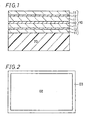
- the electromagnetic wave shielding body comprises at least a transparent electrically conductive layer (D), having at least a surface resistance of from 0.01 to 30 ⁇ /square, which has been formed on one major surface of a polymer film (B) and a transparent adhesive layer (C) formed on the other major surface of the polymer film (B), and further comprises an electrically conducting portion formed on the transparent electrically conductive layer (D), and a functional transparent layer (A) formed thereon directly or via the transparent adhesive layer.
- a transparent electrically conductive layer (D) having at least a surface resistance of from 0.01 to 30 ⁇ /square, which has been formed on one major surface of a polymer film (B) and a transparent adhesive layer (C) formed on the other major surface of the polymer film (B), and further comprises an electrically conducting portion formed on the transparent electrically conductive layer (D), and a functional transparent layer (A) formed thereon directly or via the transparent adhesive layer.
- the electromagnetic wave shielding body comprises at least a transparent electrically conductive layer (D), having at least a surface resistance of from 0.01 to 30 ⁇ /square, which has been formed on one major surface of a polymer film (B) and a functional transparent layer (A) formed on the other major surface of the polymer film (B), and further comprises a electrically conductive adhesive layer and a transparent adhesive layer (C) on the transparent electrically conductive layer (D).
- a transparent electrically conductive layer (D) having at least a surface resistance of from 0.01 to 30 ⁇ /square, which has been formed on one major surface of a polymer film (B) and a functional transparent layer (A) formed on the other major surface of the polymer film (B), and further comprises a electrically conductive adhesive layer and a transparent adhesive layer (C) on the transparent electrically conductive layer (D).
- the electromagnetic wave shielding body comprises at least a polymer film (B), a transparent electrically conductive layer (D), having at least a surface resistance of from 0.01 to 30 ⁇ /square, which has been formed on one major surface of a polymer film (B), a transparent adhesive layer (C) and a functional transparent layer (A) formed on the other major surface of the polymer film (B).
- the light control film according to the invention comprises at least a polymer film (B), a functional transparent layer (A), having an anti-reflection property and/or an anti-glare property, which has been formed on one major surface of the polymer film (B), a transparent adhesive layer (C) formed on the other major surface of the polymer film (B), and further comprises a dye, and has visible light ray transmittance of from 55 to 90%.
- a polymer film (B) functions as a substrate of a filter, for example, the substrate for forming a transparent electrically conductive layer (B) and, since a display filter according to the invention is formed directly on a surface of the display, a transparent polymer film is used.
- the polymer film (B) is not particularly limited so long as it is transparent in a visible wavelength region.
- Specific examples thereof include polyethylene terephthalate, polyethersulfone, polystyrene, polyethylene naphthalate, polyarylate, polyether ether ketone (PEEK), polycarbonate, polyethylene, polypropylene, a polyamide such as nylon 6, a polyimide, a cellulose type resin such as triacetylcellulose, polyurethane, a fluorine type resin such as polytetrafluoroethylene, a vinyl compound such as polyvinyl chloride, polyacrylic acid, a polyacrylic ester, polyacrylonitrile, an addition polymer of a vinyl compound, polymethacrylic acid, a polymethacrylate, a vinylidene compound such as polyvinylidene chloride, a vinylidene fluoride/trifluoroethylene copolymer, a vinyl compound such as ethylene/vinyl acetate copolymer
- the polymer film is ordinarily in a thickness of from 10 to 250 ⁇ m.
- the thickness of the polymer film (B) is 50 ⁇ m or more, and more preferably 75 ⁇ m or more.
- the thickness there of is more than 250 ⁇ m, flexibility is unduly scarce whereupon there is a case in which it is not suitable to utilize the film wound in roll form.
- the polymer film having a thickness of about 100 ⁇ m has broadly been used.
- the transparent polymer film to be used in the invention has flexibility whereupon a transparent electrically conductive layer can continuously be formed thereon by a roll-to-roll method; hence, a long transparent laminate having a large area can efficiently be produced. Further, a filter in film form can easily be formed directly on a surface of the display by means of lamination. Still further, it is favorable that, when a substrate glass of the display is broken, the filter, in which the polymer film is a substrate, bonded directly on the surface of the display can prevent glass pieces from being scattered.
- a surface of the polymer film (B) may previously be subjected to a sputtering treatment, a corona discharge treatment, a flame treatment, an etching treatment such as ultraviolet ray irradiation and electron beam irradiation, and prime coating thereby improving adhesiveness of the overlying transparent electrically conductive layer (D) to the polymer film (B) .
- any desired inorganic material layer for example, made of a metal or the like may be formed between the polymer film (B) and the transparent electrically conductive layer (D).
- a dust prevention treatment such as solvent cleaning and ultrasonic cleaning may be performed, before a transparent electrically conductive film is formed.
- a hard coat film (F) may have been formed on at least one major surface of the polymer film (B) so as to increase scratch resistance of the transparent laminate.
- a hard coat film which comes to be a hard coat layer (F) is a thermosetting resin, a photo-curable type resin or the like, such as an acrylic type resin, a silicone type resin, a melamine type resin, a urethane type resin, an alkyd type resin, and a fluorocarbon type resin; on this occasion, there is no particular limitation on a type and a forming method thereof. Thickness of the film is from about 1 to about 100 ⁇ m. Further, it is permissible that the hard coat layer (F) may contain at least one dye to be described below.
- a transparent electrically conductive layer (D) is formed on one major surface of a polymer film (B) .
- transparent electrically conductive layer (D) as used herein is intended to include any transparent electrically conductive film composed of a mono-layered thin film or a multi-layered thin film.
- transparent laminate (H) as used herein is intended to include any member in which the transparent electrically conductive layer (D) is formed on a major surface of the polymer film (B).
- an electrically conductive mesh such as the metallic mesh, an electrically conductive film having a lattice type pattern or a transparent electrically conductive thin film such as a metallic thin film and an oxide semiconductor thin film.
- the multi-layered transparent electrically conductive film mentioned is a multi-layered thin film in which a metallic thin film and a high-refractive-index transparent thin film are laminated to each other.
- the multi-layered thin film in which the metallic thin film and the high refractive-index transparent thin film are laminated to each other has advantageous characteristics in any one of electric conductivity, near-infrared ray cutting-off capacity and visible light ray transmittance, due to electric conductivity which a metal such as silver has and a near-infrared ray reflection characteristics which a free electron of the metal has and, further, prevention of reflection to be caused by a metal in a specified wavelength region by means of the high-refractive-index transparent thin film.
- a multi-layered thin film in which a metallic thin film having both high electric conductivity for absorbing the electromagnetic wave and a multiplicity of reflection interfaces for reflecting the electromagnetic wave, and the high-refractive-index transparent thin film are laminated to each other is preferable.
- Class A which sets a regulated limit for industrial use
- Class B which sets a regulated limit for domestic use
- the radiation-field intensity should be less than 40 dB ⁇ V/m.
- the radiation field intensity from the plasma display exceeds 40 dB ⁇ V/m in the plasma display having a diagonal size of about 20 inches and 50 dB ⁇ V/m in the plasma display having a diagonal size of about 40 inches.
- the present inventors have conducted an intensive study and found that; in order to obtain electromagnetic wave shielding capacity necessary for the plasma display as well as high visible light ray transmittance and low visible light ray reflectance, it is necessary that the transparent electrically conductive layer (D) has electric conductivity of a low resistance such that a surface resistance thereof is from 0.01 to 30 ⁇ /square, more preferably from 0.1 to 15 ⁇ /square, and still more preferably from 0.1 to 5 ⁇ /square.
- the visible light ray transmittance and the visible light ray reflectance indicate values calculated in accordance with JIS (R-3106) on the basis of the wavelength dependence of transmittance and reflectance.
- the present inventors have found that; in order to shield an intense near-infrared ray emitted from the plasma display up to such a level as causes no problem in actual use, it is required to allow a light ray transmittance minimum in a wavelength range of from 800 to 1100 nm of the near-infrared ray in the display filter to be 20% or less and, further, in order to satisfy such a requirement, it is necessary that the transparent electrically conductive layer itself has a near-infrared ray cutting-off property from the reason that a number of constitutional members is required to be decreased and there is a limitation on a near-infrared ray absorption by using a dye. Reflection by the free electron of the metal can be utilized, in order to cut off the near-infrared ray in the transparent electrically conductive layer.
- the visible light ray transmittance becomes lower, while as the metallic thin film layer becomes thinner, the reflection of the near-infrared ray becomes weaker.
- the metallic thin film layer having a given thickness is interposed between the high-refractive-index transparent thin film layers, it is possible to enhance the visible light ray transmittance and, at the same time, increase a total thickness of the metallic thin film layer.
- each layer by controlling a number of layers and/or thickness of each layer, it is possible to allow the visible light ray transmittance, the visible light ray reflectance, the near-infrared ray transmittance, a transmitted color and a reflected color to be changed within a given range.
- the transparent laminate (H) in which the transparent electrically conductive layer (D) that is a multi-layered thin film is formed on one major surface of the polymer film (B).
- a preferable transparent electrically conductive layer (D) according to the invention is formed by firstly laminating a repeating unit (Dt)/(Dm) comprising a high-refractive-index transparent thin film layer (Dt) and one metallic thin film layer (Dm) in this order on the polymer film (B) while repeating such repeating unit from 2 times to 4 times and, then, further, laminating at least one high-refractive-index transparent thin film layer (Dt) on the resultant laminate, is characterized in that a surface resistance thereof is from 0.1 to 5 ⁇ /square, and has properties excellent in low resistivity for electromagnetic wave shielding capacity, near-infrared ray cutting-off capacity, transparency, and visible light ray reflectance.
- multi-layered thin film as used herein is intended to include a transparent electrically conductive film of a multi-layered lamination in which at least one layer of a laminate constitution where a metallic thin film layer is interposed between the high-refractive-index transparent thin film layers is superimposed.
- the repeating unit is preferably laminated from 2 times to 4 times. That is, the transparent laminate (D) according to the invention in which the transparent electrically conductive layer is laminated on one major surface of the polymer film (B) has a layer constitution of (B)/(Dt)/(Dm)/(Dt)/(Dm)/(Dt), (B)/(Dt)/(Dm)/(Dt)/(Dm)/(Dm)/(Dt) or (B)/(Dt)/(Dm)/(Dt)/(Dm)/(Dm)/(Dt)/(Dm)/(Dt).
- the repeating unit When the repeating unit is laminatedmore than 5 times, a restriction on a production apparatus and productivity becomes a serious problem, and, further, there is a tendency in which the visible light ray transmittance is deteriorated and the visible light ray reflectance is increased. On the other hand, when a repeating time is one time, it is difficult to simultaneously satisfy the low resistivity, the near-infrared ray cutting-off capacity and the visible light ray reflectance.
- a surface resistance thereof is from 0.1 to 5 ⁇ /square.
- an electromagnetic wave intensity to be emitted from the plasma display is lowered in the future. In such a case, it is anticipated that, even when the surface resistance of the electromagnetic wave shielding body is from 5 to 15 ⁇ /square, sufficient electromagnetic wave shielding characteristics can be obtained. It is also conceivable that the electromagnetic wave intensity to be emitted from the plasma display is further lowered. In such a case, it is also anticipated that, even when the surface resistance of the electromagnetic wave shielding body is from 15 to 30 ⁇ /square, sufficient electromagnetic wave shielding characteristics can be obtained.
- the surface resistance of the electromagnetic wave shielding body is required to be from 0.01 to 1 ⁇ /square.
- silver As a material of the metallic thin film layer (Dm), silver is advantageous because it is excellent in electric conductivity, an infrared reflection property and visible light ray transmittance when it is laminated in multiple layers.
- silver lacks chemical and physical stability whereupon it tends to be deteriorated under actions of a contaminant, water vapor, heat, light and other factors present in the environment.
- an alloy composed of silver and at least one metal, having high environmental stability, for example, gold, platinum, palladium, copper, indium, tin or the like, and a metal which is stable to these environmental factors can favorably used.
- gold and palladium are favorable because these metals are excellent in environmental resistance and optical characteristics.
- a content of silver in such a silver-containing alloy it is desirable that the electric conductivity and optical characteristics thereof do not differ substantially from those of the silver thin film; on this occasion, the content is in a range of from about 50% by weight or more to less than about 100% by weight.
- the content is in a range of from about 50% by weight or more to less than about 100% by weight.
- Thickness of the metallic thin film layer is determined by optical design and experiment, on the basis of electric conductivity, optical characteristics and the like. No particular limitation is placed on the thickness thereof, provided that the transparent electrically conductive layer has required characteristics. However, it is necessary, based on electric conductivity and the like, that a thin film is not of an island type structure, but in a continuous state and is preferably 4 nm or more. When the metallic thin film layer is unduly thick, there occurs a problem in transparency; therefore, it is preferably 30 nm or less. When a multiple of the metallic thin film layers exist, all of such layers are not necessarily of the same thickness and do not necessarily comprise silver or an alloy thereof.
- the metallic thin film layer (Dm) there may be employed any of conventionally known methods such as sputtering, ion plating, vacuum deposition, and metal plating.
- the transparent type film constituting the high-refractive-index transparent thin film layer (Dt) so long as the transparent thin film has transparency in a visible region and have an effect of preventing light reflection in the visible region of the metallic thin film layer; however, a high-refractive-index material having a refractive index of not less than 1.6, preferably not less than 1.8, and more preferably not less than 2.0 against a visible light ray is used.
- materials which form such a transparent thin film include oxides of metals such as indium, titanium, zirconium, bismuth, tin, zinc, antimony, tantalum, cerium, neodymium, lanthanum, thorium, magnesium, and gallium; mixtures of these metal oxides; and zinc sulfide.
- the metal and an oxygen atom or a sulfur atom may be present in nonstoichiometric proportions; however, the oxides and the sulfide are permissible, so long as optical characteristics thereof are not substantially modified.
- zinc oxide, titanium oxide, indium oxide, and a mixture of indium oxide and tin oxide (ITO) are advantageously used because they not only have high transparency and a high refractive index, but also has a high-speed film formation, good adhesion to the metallic thin film layer and the like.
- Thickness of the high-refractive-index transparent thin film layer (Dt) can be determined by an optical design and an experiment, on the basis of the optical characteristics of the polymer film (B) (hereinafter referred to also as "transparent substrate"), thickness and optical characteristics of the metal thin film layer, a refractive index of the transparent thin film layer, and the like; on this occasion, although no particular limitation is placed on the thickness thereof, it is preferably in a range of from 5 to 200 nm and more preferably from 10 to 100 nm.
- Respective thickness of high-refractive-index transparent thin film layers of from a first layer to a (n+1)th layer (n being equal to or larger than 1) are not necessarily the same thereamong and, further, the high-refractive-index transparent thin film layers are not necessarily made of the same transparent thin film material.
- Dt high-refractive-index transparent thin film layer
- any desired protective layer of an organic material or an inorganic material may be provided on a surface of the transparent electrically conductive layer to such an extent as does not detract from the electric conductivity and optical characteristics thereof.
- any desired inorganic material layer may be formed between the metallic thin film layer and the high-refractive-index transparent thin film layer to such an extent as does not detract from the electric conductivity and the optical characteristics thereof.
- these inorganic materials include copper, nickel, chromium, gold, platinum, zinc, zirconium, titanium, tungsten, tin, and palladium and, further, alloys composed of two or more of these metals. Thickness thereof is preferably in a range of from about 0.2 nm to about 2 nm.
- a thin film material of each layer, a number of layers, film thickness of each layer and the like may be determined by performing an optical design which utilizes a vector method using optical constants (refractive index and extinction coefficient) of the transparent polymer film (B) and the thin film material, a method using an admittance diagram and the like while taking into consideration electric conductivity, that is, a type and thickness of the material of the metallic thin film needed for the electromagnetic wave shielding capacity to be aimed for.
- an adjacent layer which is formed on the transparent electrically conductive layer (D) is taken into consideration.
- the transparent electrically conductive layer (D) in such a manner as described above, when a bottom layer and a top layer as viewed from the polymer film (B) are thinner than any other layer interposed therebetween in the high-refractive-index transparent thin film layer (Dt), or a bottom layer as viewed from the polymer film (B) is thinner than any other layer in the metallic thin film layer (Dm) , and an adhesive which has a refractive index of from 1.45 to 1.65, a thickness of from 10 to 50 ⁇ m and an extinction coefficient of about 0 is an adjacent layer, reflectance of the transparent laminate is not significantly increased, that is, an increase of interfacial reflectance by forming the adjacent layer is 2% or less.
- the optical constant can be measured by using an ellipsometry (elliptically polarized light analytical method) or an Abbe refractometer and, further, film formation can be performed by controlling a number of layers, film thickness and the like while observing the optical characteristics.
- An atomic composition of the transparent electrically conductive layer formed in such a manner can be measured according to a method such as Auger electron spectroscopy (AES), inductively coupled plasma (ICP), and Rutherford backscattering spectrometry (RBS). Further, a layer construction and film thickness can be measured by observation in a depth direction by means of Auger electron spectroscopy, observation of a cross-section under a transmission type electron microscope, or the like.
- AES Auger electron spectroscopy
- ICP inductively coupled plasma
- RBS Rutherford backscattering spectrometry
- the film thickness is controlled by carrying out film formation on the basis of the previously established relationship between the film-forming conditions and the film formation rate, or by monitoring the film thickness during film formation by means of a quartz oscillator or the like.
- a method of using the transparent electrically conductive thin film there is also a method of using a electrically conductive mesh as the transparent electrically conductive layer.
- a mono-layer metallic mesh is described below as an example of the electrically conductive mesh, the electrically conductive mesh according to the invention is not limited to this example.
- a copper mesh layer is ordinarily formed on a polymer film.
- a copper foil is bonded on the polymer film and, then, the resultant copper foil-bonded polymer film is processed to be in a mesh state.
- Both of flat-rolled copper and electrolytic copper are usable as the copper foil to be employed in the invention; however, porous metallic layer is preferably used and, on this occasion, a pore diameter thereof is preferably from 0.5 to 5 ⁇ m, more preferably from 0.5 to 3 ⁇ m, and still more preferably from 0.5 to 1 ⁇ m.
- a pore diameter thereof is preferably from 0.5 to 5 ⁇ m, more preferably from 0.5 to 3 ⁇ m, and still more preferably from 0.5 to 1 ⁇ m.
- porosity of the copper foil is in a range of preferably from 0.01 to 20% and more preferably from 0.02 to 5%.
- porosity as used herein is intended to include a value specified by P/R, wherein R represents a volume; and P represents a pore volume.
- R represents a volume
- P represents a pore volume.
- the porosity can be defined as 1%.
- the copper foil to be used may be such a copper foil as has been subjected to any type of surface treatments. Specific examples of the surface treatments include chromate processing, surface roughening, pickling, and zinc/chromate processing.
- Thickness of the copper foil is preferably from 3 to 30 ⁇ m, more preferably from 5 to 20 ⁇ m, and still more preferably from 7 to 10 ⁇ m.
- the thickness is more than these thickness, there occurs a problem that a prolonged time is required for etching, while, when the thickness is less than these thickness, there occurs a problem that electromagnetic wave shielding capacity is deteriorated.
- An open area ratio of a light transmission part is from 60% to 95%, and more preferably from 65% to 90%, and still more preferably from 70% to 85%.
- a shape of an open area portion is not particularly limited, but it is preferable that the shape thereof is in a form of an regular triangle, a regular tetragon, a regular hexagon, a circle, a rectangle, a rhombus, or the like, shapes of such open area portions are all alike and the open area portions are aligned within a surface thereof.
- a side or a diameter thereof is in a range of, preferably from 5 to 200 ⁇ m, and more preferably from 10 to 150 ⁇ m.
- width of a metal in other portions than the open area portions is preferably from 5 to 50 ⁇ m.
- a pitch is preferably from 10 to 250 ⁇ m.
- a substantial sheet resistance of a metallic layer having the light transmission part is a sheet resistance measured by a 4-terminal method having an interval between electrodes at least 5 times as large as the repeating unit of the pattern by utilizing an electrode at least 5 times as large as the pattern.
- the open area portion has a shape of a regular tetragon having a side of 100 ⁇ m, and are regularly aligned, while the metallic layer is 20 ⁇ m wide, measurements can be conducted by disposing electrodes each having a diameter of 1 mm with an interval of 1mm therebetween.
- R resistance
- a value obtained in such a manner as described above is preferably from 0.01 ⁇ /square to 0.5 ⁇ /square, and more preferably from 0.05 ⁇ /square to 0.3 ⁇ /square.
- a transparent adhesive is used as for a method of laminating a silver foil on a polymer film.
- adhesives include those of an acrylic type, a urethane type, a silicone type, and a polyester type; however, adhesives are not particularly limited to these types.
- a two-component type and a thermosetting type are favorably used.
- the adhesive is excellent in chemical resistance. It is permissible that, after the adhesive is applied to the polymer film, the silver foil can be bonded to the resultant adhesive-applied polymer film, or the silver foil is applied with the adhesive and then bonded.
- a printing method and a photo-resist method can be used.
- the printing method it is of a common practice to allow a mask layer to form a pattern by a screen printing method utilizing a printing resist material.
- the photo-resist material is solidly formed on a metallic foil by a roll coating method, a spin coating method, an entire-surface printing method, a transfer printing method, or the like and, then, is exposed to light and developed by using photomask to perform resist patterning.
- a metallic portion which will be an opening area portion is removed by a wet etching method whereby a metallic mesh having the light transmission part of a desired opening area shape and opening area ratio can be obtained.
- Visible light ray transmittance in a light transmission portion of an electromagnetic wave shielding body is preferably from 30 to 85%, and more preferably from 50 to 80%.
- the visible light ray transmittance is less than 30%, luminance is unduly decreased to deteriorate visibility. Further, in order to obtain contrast, there are some cases in which it is necessary that the visible light ray transmittance is 85% or less, and more preferably 80% or less.
- the visible light ray transmittance in a light control film is preferably from 55 to 90%, and more preferably from 60 to 85%.
- the visible light ray transmittance is less than 55%, the luminance is unduly decreased to deteriorate the visibility.
- the visible light ray transmittance is 85% or less, and more preferably 80% or less.
- the visible light ray transmittance (Tvis) and the visible light ray reflectance (Rvis) are calculated in accordance with JIS (R-3106) on the basis of the wavelength dependence of transmittance and reflectance.
- the multi-layered thin film ordinarily lacks in a transmitted color tone.
- the electromagnetic wave shielding capacity that is, electric conductivity and near-infrared ray cutting-off capacity becomes larger, it becomes necessary to allow a total thickness of a metallic thin film to be larger.
- the total thickness of the metallic thin film becomes larger, there is a tendency in which the color becomes more of from a green color to a yellowish green color. Therefore, it is required that, in the electromagnetic wave shielding body used for a plasma display, the transmitted color thereof is neutral gray or blue gray.
- a chromaticity coordinate of white color representation on the plasma display is as near to a blackbody locus as possible.
- the transmitted color of the electromagnetic wave shielding body is neutral gray or blue gray by correcting a color tone of the multi-layered thin film.
- a correction of the color tone can be performed if only a dye having absorption in a visible wavelength region is used.
- the correction to gray can be performed by using a dye of red color
- the correction can be performed by using a dye of from blue to violet color.
- a red color luminescent phosphor such as (Y, Gd, Eu)BO 3
- a green color luminescent phosphor such as (Zn, Mn) 2 SiO 4
- a blue color luminescent phosphor such as (Ba, Eu)MgAl 10 O 17 :Eu which emit light by being excited by a vacuum ultraviolet light that is generated by direct or alternating electric current discharge in a rare gas
- the phosphors are selected on a basis of color purity, a coating property to a discharge cell, a short period of residual luminescent time, luminous efficiency, thermal resistance and the like whereupon many of the phosphors now in practical use have yet to be improved in color purity thereof.
- emission spectrum of the red color luminescent phosphor indicates several luminescent peaks over a wavelength range of from about 580 nm to about 700 nm whereupon, since a luminescent peak in a side of a relatively intense short wavelength is luminescence of from yellow color to orange color, there occurs a problem in which color purity of red color luminescence is deteriorated to approach to that of orange color luminescence.
- a mixed gas of Xe and Ne is used as a rare gas, the color purity of the orange color luminescence brought about by radiative relaxation of an Ne-excited state is also deteriorated.
- green color luminescence and blue color luminescence a position of a peak wavelength and broadness of luminescence are factors of deteriorating the color purity thereof.
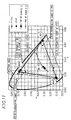
- Height of the color purity can be indicated, for example, in terms of an area of color reproduction gamut which is shown by an area of a triangle formed by connecting 3 vertices of red, green and blue colors in a coordinate system defined by Commission Internationale d'Eclairage (CIE) in which hue and saturation are represented by abscissa chromaticity x and ordinate chromaticity y, respectively. Due to a low color purity, the color reproduction gamut of luminescence of the plasma display is narrower than that which is shown by chromaticity of 3 colors of RGB defined by an NTSC (National Television System Committee) system.
- CIE Commission Internationale d'Eclairage
- a contrast ratio of the plasma display panel is from 100 to 200 at the dark and from 10 to 30 at the time of the bright occasion of about 100 lx of an environmental luminance whereupon an improvement thereof becomes a target to be pursued.
- the fact that the contrast is low is also a factor of narrowing the color reproduction gamut.
- ND neutral density
- the present inventors have found that enhancement of the color purity and contrast of the luminescent color of the color plasma display can be achieved by decreasing the unwanted luminescence and the reflection of the external light which cause to deteriorate the color purity and contrast of the luminescent color.
- an application of a dye is capable of not only controlling color of the electromagnetic wave shielding body to be neutral gray or neutral blue but also decreasing the unwanted luminescence and the reflection of the external light which cause to deteriorate the color purity and contrast of the luminescent color. Furthermore, the present inventors have found that this is particularly conspicuous when the red color luminescence is near to orange and that the color purity of the red color luminescence can be improved by decreasing the luminescence in a wavelength of from 580 nm to 605 nm which causes such deterioration.
- decrease of the unwanted luminescence and reflection of the external light can be conducted by allowing a dye having an absorption maximum in a wavelength of from 570 nm to 605 nm to be contained in the shielding body. On this occasion, it is necessary that transmission of light in a wavelength range of from 615 nm to 640 nm in which luminescence peak indicating a red color exists is not markedly impaired.
- a dye has a broad absorption range whereupon there is a risk in which even a dye having a desired absorption peak absorbs luminescence in a favorable wavelength as well by absorbing a trailing end portion thereof simultaneously.
- yellow color luminescence can be decreased to enhance the color purity of the luminescence from RGB display cells.
- green color luminescence of the color plasma display has a broad band and there is a case in which a peak position thereof exists, for example, in a side of somewhat longer wavelength than that of green color required by the NTSC system, that is, in a side of yellowish green.
- the present inventors have found that the color purity can be enhanced by absorption of a short wavelength side of a dye having an absorption maximum at a wavelength of from 570 nm to 605 nm thereby absorb-trimming a long wavelength side of the green color luminescence and, further, trimming the unwanted luminescence, and/or shifting the peak.
- minimum transmittance of the electromagnetic wave shielding body in a wavelength of from 570 nm to 605 nm is allowed to be 80% or less against a required transmittance of the red color luminescence at a peak position by using a dye having an absorption maximum in a wavelength of from 570 nm to 605 nm.
- a method of allowing a dye to be contained in the display filter according to the invention there is a method which uses at least one state selected from the group consisting of: (1) a polymer film in which at least one type of dye is kneaded in a transparent resin; (2) a polymer film prepared by first emulsify-dissolving at least one type of dye in a concentrated resin solution of a resin or a resin monomer/an organic solvent and, then, subjecting the resultant concentrated resin solution containing the dye to casting processing; (3) a material prepared by first adding at least one type of dye to a mixture of a resin binder and an organic solvent to prepare a coating material and, then, applying the thus-prepared coating material on a transparent substrate; and (4) a transparent adhesive containing at least one type of dye.
- ain as used herein is intended to include states of being contained in a substrate, in a layer such as a coating film and in an adhesive as well as states of being coated on surfaces of the substrate and the layer.
- dyes ordinary dyes or pigments which have a desired absorption wavelength in a visible region may be permissible.
- Types thereof are not particularly limited; however, examples of such dyes and pigments include organic dyes which are ordinarily available in the market such as those of an anthraquinone type, a phthalocyanine type, a methine type, an azomethine type, an oxazine type, an azo type, a styryl type, a coumarin type, a porphyrin type, a dibenzofuranone type, a diketopyrrolopyrrole type, a rhodamine type, and a xanthene type, a pyrromethene type.
- the type and concentration thereof are determined depending on an absorption wavelength/absorption coefficient of the dye, a tone of a transparent electrically conductive layer, transmission characteristics/transmittance required for the electromagnetic wave shielding body, a medium for dispersing the dye, a type/thickness of a coating film and the like; on this occasion, the type and concentration are not particularly limited.
- the transparent electrically conductive layer (D) When a multi-layered thin film is used in the transparent electrically conductive layer (D), in a case in which, though the near-infrared ray cutting-off capacity as well as the electromagnetic wave shielding capacity is held, higher near-infrared ray cutting-off capacity is required, or in another case in which the transparent electrically conductive layer does not hold the near-infrared ray cutting-off capacity, it is permissible to use one or more types of near-infrared absorption dyes together with the dyes described above in order to impart the display filter with the near-infrared ray cutting-off capacity.
- the near-infrared absorbing dye No particular limitation is placed on the near-infrared absorbing dye, so long as it can supplement the near-infrared ray cutting-off capacity of the transparent electrically conductive layer and can absorb an intense near-infrared ray emitted from the plasma display to such an extent as is suitable for practical purposes; further, no particular limitation is placed on the concentration of the near-infrared absorbing dye.
- Examples of such near-infrared absorbing dyes include compounds of a phthalocyanine type, anthraquinone type, a dithiol type, and a diiminium type.
- the dye to be used in the invention has thermal resistance, for example, such that it does not significantly deteriorate itself by being decomposed at 80°C or the like.
- a dissolving property thereof into an appropriate solvent is important. It is permissible to allow two or more types of dyes having different absorption wavelengths from each other to be contained in one medium or coating film.
- the display filter according to the invention has excellent transmission characteristics/transmittance which do not significantly impair luminance/visibility of the color plasma display and can enhance color purity and contrast of luminescent color of the color plasma display.
- the present inventors have found that, when at least one of one or more types of dyes which are to be contained is a tetraazaporphyrin compound, since the tetraazaporphyrin compound has a major absorption wavelength in a wavelength the same as or similar to that of unwanted luminescence of from 570 to 605 nm which is particularly required to be decreased and has a comparatively small absorption wavelength band, loss of luminance derived from absorption of favorable luminescence can be reduced; hence, a display filter which is excellent in capacity for enhancing transmission characteristics/transmittance, color purity and contrast of luminescence color was able to be obtained.
- the tetraazaporphyrin compound used in the invention can be expressed by the foregoing formula (1).
- the formula (1) will hereinafter be also abbreviated as the following structural formula (2): wherein A m and A n each individually represent a hydrogen atom, a halogen atom, a nitro group, a cyano group, a hydroxy group, an amino group, a carboxyl group, a sulfonic acid group, an alkyl group having carbon atoms of from 1 to 20, a halogenoalkyl group, an alkoxy group, an alkoxyalkoxy group, an aryloxy group, a monoalkylamino group, dialkylamino group, an aralkyl group, an aryl group, a heteroaryl group, an alkylthio group, or arylthio group; A m and A n each individually may form a ring except an aromatic ring via a connecting group; and M represents two hydrogen atoms, a
- tetraazaporphyrin compound expressed by the formula (1) include a hydrogen atom; halogen atoms such as fluorine, chlorine, bromine and iodine atom; a nitro group; a cyano group; a hydroxy group; an amino group; a carboxyl group; a sulfonic acid group; linear-chain, branched-chain or cyclic alkyl groups each having carbon atoms of from 1 to 20 such as a methyl group, an ethyl group, an n-propyl group, an iso-propyl group, an n-butyl group, an iso-butyl group, a sec-butyl group, a t-butyl group, an n-pentyl group, a 2-methylbutyl group, a 1-methylbutyl group, a neo-pentyl group, a 1,2-di
- Examples in which combinations of A 1 and A 2 , A 3 and A 4 , A 5 and A 6 , and A 7 and A 8 each form a ring via a connecting group include -CH 2 CH 2 CH 2 CH 2 -, -CH 2 CH 2 CH (NO 2 ) CH 2 -, -CH 2 CH(CH 3 ) CH 2 CH 2 -, and - CH 2 CH(Cl)CH 2 CH 2 -.
- divalent metals shown as M include Cu, Zn, Fe, Co, Ni, Ru, Rh, Pd, Pt, Mn, Sn, Mg, Hg, Cd, Ba, Ti, Be, and Ca.
- trivalent metals each having one substituent examples include Al-F, Al-Cl, Al-Br, Al-I, Ga-F, Ga-Cl, Ga-Br, Ga-I, In-F, InCl, In-Br, In-I, Tl-F, Tl-Cl, Tl-Br, Tl-I, Al-C 6 H 5 , Al-C 6 H 4 (CH 3 ), In-C 6 H 5 , In-C 6 H 4 (CH 3 ), Mn (OH), Mn (OC 6 H 5 ), Mn[OSi(CH 3 ) 3 ], and Fe-Cl, Ru-Cl.
- Examples of tetravalent metals each having two substituents include CrCl 2 , SiF 2 , SiCl 2 , SiBr 2 , SiI 2 , SnF 2 , SnCl 2 , SnBr 2 , ZrCl 2 , GeF 2 , GeCl 2 , GeBr 2 , GeI 2 , TiF 2 , TiCl 2 , TiBr 2 , Si(OH) 2 , Sn(OH) 2 , Ge(OH) 2 , Zr(OH) 2 , Mn(OH) 2 , TiA 2 , CrA 2 , SiA 2 , SnA 2 , and GeA 2 , wherein A represents any one of an alkyl group, a phenyl group, a naphthyl group and a derivative thereof; and Si(OA') 2 , Sn(OA') 2 , Ge(OA') 2 , Ti(OA') 2 , and Cr(OA') 2 , where
- Examples of oxy metals include VO, MnO, and TiO.
- Y represents any one of a halogen atom, an alkoxy group, an aryloxy group, an acyloxy group, a hydroxy group, an alkyl group, an aryl group, an alkylthio group, an arylthio group, a trialkylsilyloxy group, a trialkyl tin oxyo group, and a trialkyl germanium oxy group.
- the present inventors have further found that, when the azaporphyrin compound expressed by the formula (1) is, for example, a tetra-t-butyl-tetraazaporphyrin complex or a tetra-neo-pentyl-tetraazaporphyrin complex, the compound is comparatively easily produced, a dissolving property thereof against a solvent and the complex itself are stable, the compound is excellent in absorption characteristics and, as a result of having been imparted with a t-butyl group or a tetra-neo-pentyl group, the compound is allowed to have a third dimensional form which enhances the dissolving property against a solvent and, accordingly, the dye has come to be easily contained and, on the basis of this finding, an excellent electromagnetic wave shielding body was able to be obtained.
- the azaporphyrin compound expressed by the formula (1) is, for example, a tetra-t-butyl-tetraazaporphy
- the methods (1) to (4) which allow the dye to be contained can be conducted in at least one layer selected from the group consisting of a polymer film (B) containing a dye, a transparent adhesive layer (C) or a second transparent adhesive layer containing a dye to be described below, a functional transparent layer (A) containing a dye to be described below, and the hard coat layer (F), containing a dye, which has been described above.
- the functional transparent layer (A) containing a dye to be described below may be any one of a film which contains a dye and, further, has various types of functions, a material in which a film which contains a dye and, further, has various types of functions is formed on a polymer film, and a material in which a film having various types of functions is formed on a substrate containing a dye.
- At least two types of dyes having different absorption wavelengths from each other may be contained in a medium or a coating film, or at least two dye layers may be present.
- a resin material which has transparency as high as possible when formed into a plastic plate or a polymer film.
- resin materials include, but are not limited to, polyethylene terephthalate, polyether sulfone, polystyrene, polyethylene naphthalate, polyarylate, polyether ether ketone, polycarbonate, polyethylene, polypropylene, polyamides such as nylon 6, polyimides, cellulose type resins such as triacetylcellulose, polyurethane, fluorine-containing compounds such as polytetrafluoroethylene, vinyl compounds such as polyvinyl chloride, polyacrylic acid, polyacrylic esters, polyacrylonitrile, addition polymers of vinyl compounds, polymethacrylic acid, polymethacrylate, vinylidene compounds such as polyvinylidene chloride, copolymers of vinyl compounds or fluorine-containing compounds such as a vinylidene fluoride/trifluoroethylene copolymer, and an ethylene/vinyl
- a processing temperature, a film-forming condition and the like may vary somewhat according to a dye used and a base polymer.
- usually employed are (i) a method in which a dye is mixed to powders or pellets of a base polymer, and the resulting mixture is heat-melted at a temperature of from 150 to 350°C and formed into a plastic plate; (ii) a method in which a film is formed by an extruder; (iii) a method in which a raw film is prepared by an extruder and, then, uniaxially or biaxially stretched to a size 2 to 5 times an original size at a temperature of from 30 to 120°C to form a film having a thickness of from 10 to 200 ⁇ m, and the like.
- An additive commonly used at the time of molding resins such as a plasticizer, may be added during kneading.
- an amount of the dye to be added may vary according to absorption coefficient of the dye, thickness of a polymeric molded article to be made, intended absorption intensity, intended transmission characteristics/transmittance and the like, it usually ranges from 1 ppm to 20%, based on the weight of the polymeric molded article as a substrate.
- a dye is add-dissolved in a concentrated solution of resin in which a resin or a resin monomer is dissolved in an organic solvent and, on this occasion, a plasticizer, a polymerization initiator, or an anti-oxidant is added, as desired, and the resultant concentrated solution is poured onto a mold or a drum which has a required surface contour to obtain a plastic plate or a polymer film through subsequent solvent evapolation/drying or polymerization/solvent evapolation/drying processing.
- a solvent selected from the group consisting of solvents of a halogen type, an alcohol type, a ketone type, an ester type, an aliphatic hydrocarbon type, an aromatic hydrocarbon type, an ether type and a mixture type thereof.
- a concentration of the dye may vary according to absorption coefficient of the dye, thickness of the plate or the film, intended absorption intensity, intended transmission characteristics/transmittance and the like, it is usually in a range of from 1 ppm to 20%, based on the weight of the resin monomer.
- a concentration of the resin is usually in a range of from 1 to 90%, based on the entire coating material.
- a method (3) which comprises preparing a coating material and, then, performing a coating operation
- employed are a method in which a dye is dissolved in a binder resin and an organic solvent to prepare a coating material, a method in which a dye that has previously been pulverized (50 to 500 nm) is dispersed in an uncolored acrylic emulsion-based coating material to prepare an acrylic emulsion-based aqueous coating material and the like.
- a solvent selected from the group consisting of: solvents of a halogen type, an alcohol type, a ketone type, an ester type, analiphatic hydrocarbon type, an aromatic hydrocarbon type, an ether type and a mixture type thereof.
- a concentration of the dye may vary according to absorption coefficient of the dye, thickness of such coating, intended absorption intensity, intended visible light transmittance and the like, it is usually in a range of from 0.1 to 30%, based on the weight of the binder resin.
- a concentration of the binder resin is usually in a range of from 1 to 50%, based on the entire coating material.
- the acrylic emulsion-based aqueous coating material in a latter method can also be obtained, in the same way as in the former method, by dispersing a dye which has previously been pulverized (50 to 500 nm) in an uncolored acrylic emulsion-based coating material.
- An additive commonly used in a coating material, such as an antioxidant, may be added to the coating material.
- the coating material prepared according to any one of the methods is applied on a transparent polymer film, a transparent resin, a transparent glass or the like by means of a bar coaler, a blade coater, a spin coater, a reverse coater, a die coater, a spray gun or the like in a known coating manner to prepare a substrate containing a dye.
- a protective layer may be provided on a coated surface in order to protect a coated surface, or another component of the electromagnetic wave shielding body may be bonded to the coated surface in such a manner as to protect the coated surface.
- an adhesive or glue in sheet form or in liquid form such as an acrylic adhesive, a silicone type adhesive, a urethane type adhesive, a polyvinyl butyral adhesive (PVB), and an ethylene-vinyl acetate (EVA) type adhesive, a polyvinyl ether, a saturated amorphous polyester, a melamine resin or the like after being added with a dye of from 10 ppm to 30%.
- an adhesive or glue in sheet form or in liquid form such as an acrylic adhesive, a silicone type adhesive, a urethane type adhesive, a polyvinyl butyral adhesive (PVB), and an ethylene-vinyl acetate (EVA) type adhesive, a polyvinyl ether, a saturated amorphous polyester, a melamine resin or the like after being added with a dye of from 10 ppm to 30%.
- an ultraviolet ray absorbing agent in order to enhance light resistance of the electromagnetic wave shielding body containing the dye, an ultraviolet ray absorbing agent can also be contained together with the dye.
- a type and a concentration of the ultraviolet absorbing agent are not particularly limited.
- an optional transparent adhesive layer is interposed within a laminate.
- a transparent adhesive layer (C) according to the invention or the like is a layer comprising an optional transparent adhesive or glue.
- an acrylic adhesive e.g., a silicone type adhesive, a urethane type adhesive, a polyvinyl butyral adhesive (PVB), an ethylene-vinyl acetate (EVA) type adhesive and the like, a polyvinyl ether, a saturated amorphous polyester, a melamine resin and the like. It is important, on this occasion, that the adhesive to be used in a central portion that is a portion which a light ray emitted from the display passes through is required to be sufficiently transparent against a visible light ray.
- the electrically conductive adhesive layer is an adhesive layer for the purpose of electrically connecting a transparent electrically conductive layer (D) with an earth portion (ground conductor) of a display apparatus; on this occasion, though it is necessary that the electrically conductive adhesive layer is electrically conductive, it is not necessary that the electrically conductive adhesive layer is transparent. Since it is necessary that, in the electromagnetic wave shielding body, a transparent electrically conductive layer (D) is electrically connected with an external member, the transparent adhesive layer should not significantly interfere with such an electrical connection due to the electrically conductive adhesive layer. Namely, an electrically conducting portion in which the transparent adhesive layer is not formed on the transparent electrically conductive layer (D) is necessary. For example, it is important that the transparent adhesive layer is formed such that a peripheral portion of the transparent electrically conductive layer (D) is left intact to allow it to be the conducting portion.
- the electrically conductive adhesive or the electrically conductive adhesive to be used in the electrically conductive adhesive layer comprises a base agent such as an acrylic adhesive, a silicone type adhesive, a urethane type adhesive, a polyvinyl butyral adhesive (PVB), and an ethylene-vinyl acetate (EVA) type adhesive, apolyvinyl ether, a saturated amorphous polyester, a melamine resin or the like, and carbon or metallic particles of Cu, Ni, Ag, Fe or the like dispersed in the base agent as electrically conductive particles.
- a base agent such as an acrylic adhesive, a silicone type adhesive, a urethane type adhesive, a polyvinyl butyral adhesive (PVB), and an ethylene-vinyl acetate (EVA) type adhesive, apolyvinyl ether, a saturated amorphous polyester, a melamine resin or the like, and carbon or metallic particles of Cu, Ni, Ag, Fe or the like dispersed in the base agent as electrically
- volume resistivity of the electrically conductive adhesive or the electrically conductive adhesive to be used is from 1 ⁇ 10 -4 to 1 ⁇ 10 3 ⁇ cm.
- a sheet state or a liquid form thereof is permissible so long as there exists practical adhesive strength therein.
- a pressure-sensitive type adhesive in sheet form is favorably used as the adhesive. After such an adhesive in sheet form is bonded or an adhesive method is applied, bonding is performed by lamination.
- the liquid form is such an adhesive as is cured by being left to stand at room temperature, being heated or being irradiated by an ultraviolet ray after being applied and bonded.
- application methods mentioned are various types of methods such as a screen printing method, a bar coating method, a reverse coating method, a gravure coating method, a die coating method, and a roll coating method; however, such an appropriate application method is usually chosen by taking into consideration a type, a viscosity, an application amount and the like of the adhesive.
- thickness of a layer thereof the thickness is, in view of the volume resistivity and a required electrically conductive property, in a range of from 0.5 ⁇ m to 50 ⁇ m and preferably from 1 ⁇ m to 30 ⁇ m.
- an electrically conductive tape of a double-faced adhesion type having an electrically conductive property on both faces which is available in the market can also favorably be used.
- thickness of this layer is in a range of from about several micrometers to about several millimeters.
- the adhesive may either be in sheet form or liquid form, so long as it has a practical adhesion strength.
- a pressure-sensitive type adhesive in sheet form is favorably used as the adhesive. After such an adhesive in sheet form is bonded or an adhesive material is applied, a bonding method is performed by laminating individual members with each other.
- the liquid form is such an adhesive as is cured by being left to stand at room temperature or being heated after being applied and bonded.
- the thickness is in a range of from 0.5 ⁇ m to 50 ⁇ m and preferably from 1 ⁇ m to 30 ⁇ m. Further, it is preferable that a surface on which the transparent adhesive layer is formed or a surface to be bonded therewith is beforehand subjected to a treatment for allowing adhesion to be easily performed such as coating for the purpose of easy adhesion and a corona discharge treatment thereby enhancing a wetting property thereof.
- the transparent adhesive layer in order to remove air entrapped between members at the time of bonding, or to perform solution treatment on the adhesive and, further, to enhance adhesion strength between members, it is important that curing is performed under conditions of pressure and heating, if possible.
- the condition of pressure is from about several to 20 atms; further, although the condition of heating depends on thermal resistance of individual members, it is from about room temperature to about 80°C. However, no particular limitations are placed on these conditions.
- At least one layer of the transparent adhesive layers is allowed to contain a dye.
- the display filter according to the invention has at least one function selected from the group consisting of a hard coat property, an anti-reflection property, an anti-glare property, an antistatic property, an anti-fouling property, a gas barrier property and an ultraviolet ray cutting-off property and, further, in the display filter, a functional transparent layer (A) which a visible light ray passes through is formed on a transparent electrically conductive layer (D) either directly or via a second transparent adhesive layer. It is preferable that one functional transparent layer (A) has a plurality of functions.
- the functional transparent layer (A) according to the invention may be a functional film itself having at least one of the functions described above, a transparent substrate on which a functional film has been formed by a coating method, a printing method, or various types of known film-forming methods, or a transparent substrate having various types of functions.
- the functional film is formed directly on a major surface of the transparent electrically conductive layer (D) which forms the functional transparent layer (A) by a coating method, a printing method or various types of other known film-forming methods.
- bonding may be performed on a major surface of the transparent electrically conductive layer (D) either via an adhesive or via the adhesive containing a dye.
- D transparent electrically conductive layer
- the transparent substrate is a transparent polymer film; on this occasion, no particular limitation is placed on a type and thickness thereof and, further, a dye can be contained in the transparent substrate. Even in a case in which the functional transparent layer (A) is the functional film itself, the dye can also be contained in the film.
- the functional transparent layer (A) should not interfere with such an electrical connection. Namely, an electrically conducting portion in which the functional transparent layer (A) is not formed on the transparent electrically conductive layer (D) is necessary.
- the functional transparent layer (A) is formed such that a peripheral portion of the transparent electrically conductive layer is left intact to allow the peripheral portion to be the conducting portion.
- the functional transparent layer (A) has at least one function of an anti-reflection (hereinafter referred to also as AR) property for suppressing reflection of an external light, an anti-glare (hereinafter referred to also as AG) property, and an anti-reflection/anti-glare (hereinafter referred to also as ARAG) property which is imparted with both of the foregoing two properties.
- AR anti-reflection
- AG anti-glare
- ARAG anti-reflection/anti-glare
- elements constituting an anti-reflection film and respective film thickness of the elements are determined by carrying out an optical design with consideration for optical characteristics of the substrate on which this anti-reflection layer is formed.
- an inorganic compound such as a metal oxide, a fluoride, a silicide, a boride, a carbide, a nitride,
- Such a single-layered one is easily prepared, but is inferior to such a laminate of two or more layers in the anti-reflection property.
- a laminate of 4 layers has anti-reflection capacity over a wide wavelength range and undergoes less restriction in the optical design based on the optical characteristics of the substrate.
- any one of conventionally known methods such as sputtering, ion plating, vacuum deposition, and wet coating can be adopted.
- any one of conventionally known methods such as a method of dry-curing after wet coating, for example, a bar coating method, a reverse coating method, a gravure coating method, a die coating method, and a roll coating method can be adopted.
- Visible light ray reflectance of a surface of the functional transparent layer (A) having an anti-reflection property is 2% or less, preferably 1.3% or less, and more preferably 0.8% or less.
- the functional transparent layer (A) having an anti-glare (AG) property indicates a transparent layer which is transparent to a visible light ray and is provided with minute surface irregularities having a size of from about 0.1 ⁇ m to about 10 ⁇ m.
- the functional transparent layer (A) having the anti-glare property is formed by first dispersing particles of an inorganic or organic compound such as silica, an organosilicon compound, melamine, and an acrylate in a thermosetting or photo-curable resin such as an acrylic type resin, a silicone type resin, a melamine type resin, a urethane type resin, an alkyd type resin, and a fluorine type resin to prepare ink and, then, applying the thus-prepared ink to the substrate according to a method such as a bar coating method, a reverse coating method, a gravure coating method, a die coating method, and a roll coating method and, thereafter, curing the thus-applied ink.
- a thermosetting or photo-curable resin such as an acrylic type resin, a silicone type resin, a melamine type resin, a urethane type resin, an alkyd type resin, and a fluorine type resin
- the anti-glare property can also be obtained by first coating a substrate with a thermosetting or photo-curable resin such as an acrylic type resin, a silicone type resin, a melamine type resin, a urethane type resin, an alkyd type resin, and a fluorine type resin and, then, pressing the thus-coated substrate against a mold having a desired haze or a surface contour and, thereafter, curing the resin.
- a thermosetting or photo-curable resin such as an acrylic type resin, a silicone type resin, a melamine type resin, a urethane type resin, an alkyd type resin, and a fluorine type resin.
- the functional transparent layer (A) having the anti-glare property has appropriate surface irregularities and is not particularly limited to the methods described above.
- a haze of the anti-glare property is from 0.5% to 20% and preferably from 1% to 10%.
- the anti-glare property becomes insufficient, while, when the haze is unduly high, transmittance of parallel light rays is reduced whereupon the visibility of the display is deteriorated.
- the functional transparent layer (A) having the anti-reflection/anti-glare (ARAG) property can be obtained by forming the anti-reflection film on a film having an anti-glare property or a substrate.
- the film having the anti-glare property is a film having a high refractive index, even when the anti-reflection film is made of a mono layer, the functional transparent layer (A) can be imparted with a relatively high anti-reflection property.
- Prevention of reflection by the AR or the ARAG can enhance the light ray transmittance of the display filter.
- the display filter according to the invention is bonded to a representation portion of the display via the transparent adhesive layer (C), reflection of a substrate glass on a surface of the representation portion is avoided. Therefore, furthermore, the filter in which the functional transparent layer (A) having a function of AR or ARAG is formed has a low reflection on a surface thereof whereupon contrast and color purity of the display can further be enhanced. Reflectance of the visible light ray on the surface of the functional transparent layer (A) having the functions of the AR or the ARAG is 2% or less, preferably 1.3% or less, and more preferably 0.8% or less.
- the functional transparent layer (A) has a hard coat property.
- a hard coat film mentioned are films of thermosetting type resins and photo-curable resins such as an acrylic type resin, a silicone type resin, a melamine type resin, an urethane type resin, an alkyd type resin, and a fluorine type resin; however, no particular limitation is placed on a type and a forming method thereof.
- a thickness of these films is from about 1 to about 100 ⁇ m.
- the functional transparent layer (A) may have both of the anti-reflection property and the hard coat property either by allowing the hard coat film to be used in the high refractive-index layer or a low refractive-index layer of the functional transparent layer (A) having the anti-reflection property or by allowing the anti-reflection film to be formed on the hard coat film.
- the functional transparent layer (A) may have both of the anti-glare property and the hard coat property.
- a surface hardness of the functional transparent layer (A) having the hard coat property is at least H, preferably 2H, and more preferably 3H or more in terms of pencil hardness in accordance with JIS (K-5400).
- the surface of the display filter tends to attract dust owing to electrostatic charge and, moreover, such static electricity may be discharged upon contact with a human body to give an electric shock thereto. Accordingly, it may be required to subject the display filter to an antistatic treatment.
- the functional transparent layer (A) may have electric conductivity. On this occasion, it is sufficient to allow electric conductivity to be about 10 11 ⁇ /square or less in terms of a surface resistance, but the surface resistance should not detract from transparency or resolution of a display screen.
- the electrically conductive layer mentioned are a well-known transparent electrically conductive film such as an ITO and an electrically conductive film in which electrically conductive ultrafine particles such as ultrafine particles of ITO and ultrafine particles of tin oxide are dispersed.
- a layerwhich constitutes the functional transparent layer (A) having at least one function selected from the group consisting of the anti-reflection property, the anti-glare property, the anti-reflection/anti-glare property, and a hard coat property has electric conductivity.
- Such films having a gas barrier property include thin films of metal oxides such as silicon oxide, aluminum oxide, tin oxide, indium oxide, yttrium oxide, and magnesium oxide, and mixtures thereof; thin films of these metal oxides added with a slight amount of other elements; and those made of polyvinylidene chloride, an acrylic type resin, a silicone type resin, amelamine type resin, an urethane type resin, a fluorine type resin or the like.
- these thin films or the films are not necessarily limited thereto.
- Thickness of these films is in a range of from 10 to 200 nm in a case of thin films each made of a metal oxide and from about 1 to about 100 ⁇ m in a case of the films each made or a resin, and these thin films or films may have either a mono-layer or a multi-layered structure.
- the thickness and structure of these thin films or films are not limited to those described above.
- polymer films having low moisture permeability include those made of polyethylene, polypropylene, nylon, polyvinylidene chloride, a vinylidene chloride/vinyl chloride copolymer, a vinylidene chloride/acrylonitrile copolymer, and a fluorine type resin.
- the polymer films are not particularly limited to these materials, so long as the moisture permeability thereof is not greater than 10 g/m 2 ⁇ day. Even when the polymer film has a relatively high moisture permeability, the moisture permeability can be reduced by increasing the thickness of the film or adding an appropriate additive thereto.
- a layer constituting the functional transparent layer (A) having at least one property selected from the group consisting of: the anti-reflection property, the anti-glare property, the anti-reflection/anti-glare property, and an antistatic property, an anti-Newton ring property, and the hard coat property is a film having a gas barrier property, or a whole body or, when used concurrently with an adjacent transparent adhesive layer, the layer has the gas barrier property.
- the functional transparent layer (A) containing a dye and having the anti-reflection property, the hard coat property, the antistatic property and the gas barrier property mentioned is a polyethylene terephthalate film containing a dye/hard coat film/ITO/silicon-containing compound/ITO/silicon-containing compound, and the like.
- the functional transparent layer (A) having the anti-reflection/anti-glare property, the hard coat property, the antistatic property and the gas barrier property mentioned are a layer made of triacetyl cellulose film/hard coat film in which fine particles of ITO are dispersed/a silicon-containing compound, and the like.
- a surface of the functional transparent layer (A) may have an anti-fouling property such that stainproof against a fingerprint and the like is imparted thereto or, when a stain is attached thereto, it can easily be removed therefrom.
- a material having the anti-fouling property is such a material as having a non-wetting property for water and/or oils and fats; for example, a fluorine compound, and a silicon compound are mentioned. When other functions such as the anti-reflection, and antistatic property are concurrently taken into consideration, the material should not interfere with these functions.
- the surface of the functional transparent layer (A) can be imparted with the anti-fouling property while maintaining the anti-reflection property and the antistatic property by using a fluorine compound which has a low refractive index as a constituting material of an anti-reflection film, or coating an outermost surface thereof with a fluorine type organic molecule of from 1 to several molecules.
- the functional transparent layer (A) having the anti-fouling property, the anti-reflection property, the hard coat property, the antistatic property and the gas barrier property mentioned are a mono-molecule coated film of a hard coat film/ITO/silicon-containing compound/ ITO/silicon-containing compound/a film coated with a mono fluorine type organic molecule, and the like.
- the functional transparent layer (A) has an ultraviolet ray cutting-off property.
- an anti-reflection film comprising a mono-layer or multi-layer of an inorganic thin film which absorbs the ultraviolet ray, a substrate constituting a functional transparent film which contains an ultraviolet ray absorbing agent, and the functional transparent layer (A) having a hard coat film are suitable to this case. No particular limitation is placed on a type and a concentration of the ultraviolet ray absorbing agent.
- At least one of the transparent adhesive layers may contain the ultraviolet ray absorbing agent.
- the ultraviolet cutting-off property may vary according to durability of the dye and is not particularly limited.
- rigidity of the optical filter film is mainly controlled by the total thickness of the transparent polymer film, it is surmised that an effect according to the present invention is attributable to an effect of the bending moment. Further, with increase of the rigidity of the optical filter film, such removal can continuously be performed by a uniform strength whereupon paste remaining which would start from a removal break point on the glass plate is hardly generated.
- the total thickness of the transparent polymer film becomes larger, impact resistance thereof is enhanced more; however, as a number of laminating layers becomes larger, production efficiency becomes lower whereupon, with substantial increase of the rigidity thereof, it becomes difficult to bond it direct on the display. Therefore, though the total thickness of the transparent polymer film is not particularly limited, but it is in a range of preferably from 0.3 to 1.0 mm and more preferably from 0.4 to 0.8 mm. Further, though the number of the laminating layers is not particularly limited, but it is in a range of preferably from 2 to 6 and more preferably from 2 to 4.
- FIGS. 12 to 17 are cross-sectional diagrams each showing an example of a constitution of a display filter according to the invention.
- a transparent adhesive layer 30, a transparent polymer film (B) 23 (150 ⁇ m) having near-infrared shielding capacity, a transparent adhesive layer 30, a transparent polymer film (B) 24 (188 ⁇ m) having a functional transparent layer (A) showing an anti-reflection function are laminated in this order to constitute a display filter.
- a transparent adhesive layer 30, a transparent polymer film (B) 25 (200 ⁇ m) for increasing a total thickness, a transparent adhesive layer 30, a transparent polymer film (B) 23 (75 ⁇ m) having near-infrared shielding capacity, a transparent adhesive layer 30, a transparent polymer film (B) 24 (80 ⁇ m) having a functional transparent layer (A) showing an anti-reflection function are laminated in this order to constitute a display filter.
- a transparent adhesive layer 30, a transparent polymer film (B) 23 (75 ⁇ m) having near-infrared shielding capacity, a transparent adhesive layer 30, a transparent polymer film (B) 25 (200 ⁇ m) for increasing a total thickness, a transparent adhesive layer 30, a transparent polymer film (B) 24 (80 ⁇ m) having a functional transparent layer (A) showing an anti-reflection function are laminated in this order to constitute a display filter.
- a transparent adhesive layer 30, a transparent polymer film (B) 25 (200 ⁇ m) for increasing a total thickness, a transparent adhesive layer 30, a functional transparent layer (A) showing an anti-reflection function, a transparent polymer film (B) 26 (150 ⁇ m) having near-infrared shielding capacity are laminated in this order to constitute a display filter.
- a transparent adhesive layer 30, a transparent polymer film (B) 25 (200 ⁇ m) for increasing a total thickness, a transparent adhesive layer 30, a transparent polymer film (B) 23 (75 ⁇ m) having a transparent electrically conductive layer (D) showing an electromagnetic wave shielding function, a transparent adhesive layer 30, a transparent polymer film (B) 24 (150 ⁇ m) having a functional transparent layer (A) showing an anti-glare function are laminated in this order to form an electrode 50 on the transparent polymer film 23 thereby constituting a display filter.
- a transparent adhesive layer 30, a transparent polymer film (B) 25 (200 ⁇ m) for increasing a total thickness, a transparent adhesive layer 30, a transparent polymer film (B) 26 (188 ⁇ m) having a functional transparent layer (A) showing an anti-reflection function and a transprarent electrically conductive layer (D) showing an electromagnetic wave shielding function are laminated in this order to form an electrode 50 on the transparent polymer films 25 and 26 thereby constituting a display filter.
- FIG. 18 is a cross-sectional diagram showing a constitution of the transparent polymer film (B) 23 showing an electromagnetic wave shielding function shown in FIG. 16.
- a transparent electrically conductive layer (D) 10 showing an electromagnetic wave shielding function; on this occasion, the transparent electrically conductive layer (D) 10 is constituted by laminating a transparent thin film layer (Dt) 11 having a high refractive index and a metallic thin film layer (Dm) 12 comprising silver or a silver alloy in an order of Dt/Dm/Dt/Dm/Dt.
- a transparent adhesive layer 30 which enables the filter to be adhered to the display screen.
- FIG. 19 is a cross-sectional diagram showing a constitution of a transparent polymer film (B) 26 showing an electromagnetic wave shielding function shown in FIG. 17.
- a transparent electrically conductive layer (D) 10 showing an electromagnetic wave shielding function; on this occasion, the transparent electrically conductive layer (D) 10 is constituted by laminating a transparent thin film layer (Dt) 11 having a high refractive index and a metallic thin film layer (Dm) 12 comprising silver or a silver alloy in an order of Dt/Dm/Dt/Dm/Dt/Dm/Dt.
- an anti-reflection film 61 is a functional transparent layer (A) .
- a transparent adhesive layer 30 which enables the filter to be adhered to the display screen.
- FIG. 20 is a plan view of the display filter shown in FIGS. 16 and 17.
- the filter is rectangular in form, and an image represented on the display is observed through a central portion of the filter.
- an electrode 50 which is electrically connected with a transparent electrically conductive layer; on this occasion, the electrode 50 is connected with a ground terminal of the display.
- an electromagnetic wave is shielded by disposing a metal layer inside a case of the equipment or by using the case made of an electrically conductive material.
- a window-like electromagnetic wave shielding body in which a transparent electrically conductive layer is formed is disposed. Since the electromagnetic wave absorbed in the electrically conductive layer induces electric charge, this electric charge must be escaped by grounding the electrically conductive layer. Otherwise the electromagnetic wave shielding body acts as an antenna for emitting electromagnetic waves, resulting in a reduction in electromagnetic wave shielding capacity. Accordingly, it is necessary that the electromagnetic wave shielding body and a ground portion of a main body of the display are electrically connected with each other.
- the transparent adhesive layer (C) and the functional transparent layer (A) are formed on the transparent electrically conductive layer (D) as shown in FIG. 3, it is preferable that the transparent adhesive layer (C) and the functional transparent layer (A) are formed on the transparent electrically conductive layer (D) such that an electrically conducting portion is left.
- the term "electrode” as used herein is intended to include an electrically conducting portion in the electromagnetic wave shielding body for an external member.
- the electrode may be an exposed portion of the transparent electrically conductive layer or be made either by printing a metallic past having an electrically conductive property on the exposed portion or by bonding an electrically conductive material such as an electrically conductive tape, an electrically conductive adhesive to the exposed portion for the purpose of protection thereof and a favorable electric connection.
- the electrode may be formed on the functional transparent layer such that it can secure an electric connection with the transparent electrically conductive layer. As described above, thought no particular limitation is placed on a shape or a material of the electrode, it is preferable that the electrode is formed such that the exposed portion of the transparent electrically conductive layer is covered by the electrically conductive material.
- the electrode according to the invention may be obtained by contacting the electrically conductive material with a cross-sectional portion of a film comprising the transparent electrically conductive layer according to the invention.
- the cross-sectional portion that is, the cross-sectional portion of the film comprising the transparent electrically conductive layer in which at least the transparent electrically conductive layer and a film for protecting it are stratified can be observed, and a desired electrode can be obtained so long as an appropriate electrically conductive material is in contact with the transparent electrically conductive layer in the cross-sectional portion.
- FIGS. 21 to 25 are each a cross-sectional diagram showing an example of a constitution of a display filter according to the invention.
- a transparent adhesive layer 30, a transparent polymer film (B) 23, a transparent electrically conductive layer (D) 10, and an anti-glare film 71 which is a functional transparent layer (A) are laminated in this order to form an electrode 50 on the transparent electrically conductive layer (D) 10 thereby constituting a display filter.
- an anti-glare film 71 which is a functional transparent layer (A), a transparent polymer film (B) 23, a transparent electrically conductive layer (D) 10 are laminated in this order to form an electrode 50 in a periphery of the transparent electrically conductive layer (D) 10.
- a transparent adhesive layer 30 is disposed in a central portion thereof excluding the electrode 50 thereby allowing the resultant laminate to be bonded to a display screen.
- a transparent adhesive layer 30, a transparent polymer film (B) 23, a transparent electrically conductive layer (D) 10, and an anti-glare film 71 which is a functional transparent layer (A) are laminated in this order to form an electrode 50 on an end surface of a side edge of the resultant laminate thereby constituting a display filter.
- a transparent adhesive layer 30, a transparent electrically conductive layer (D) 10, a transparent polymer film (B) 23, an anti-glare film 71 which is a functional transparent layer (A) are laminated in this order whereupon an electrically conductive tape 51 such as a copper tape is interposed between the transparent adhesive layer 30 and the transparent electrically conductive layer (D) 10 to secure an electrical connection to the transparent electrically conductive layer (D) 10 via a filter peripheral portion.
- an electrically conductive tape 51 such as a copper tape
- a transparent adhesive layer 30, a transparent electrically conductive layer (D) 10, a transparent polymer film (B) 23, an anti-glare film 71 which is a functional transparent layer (A) are laminated in this order whereupon a through-hole electrode 52 is formed in a direction of thickness of a filter thereby securing an electrical connection to the transparent electrically conductive layer (D) 10.
- FIG. 26 is a plan view of the display filter shown in FIGS. 21 to 25.
- the filter is rectangular in form, and an image represented on the display is observed by allowing it to pass through a central portion of the filter.
- electrodes 50, electrically conductive tapes 51 or through-hole electrodes 52 which are electrically connected with a transparent electrically conductive layer; on this occasion, these electrodes are connected with a ground terminal of the display.
- an electrode of the display filter shown in FIGS. 21 to 25 may, needless to mention, be disposed in an entire periphery of the filter in the same manner as in the plan view shown in FIG. 20.
- an electrically conductive tape such as a copper tape is interposed between the transparent electrically conductive layer and the transparent adhesive layer to be bonded thereon to form an electrode by drawing out a portion of the electrically conductive tape to an outside of the electromagnetic wave shielding body.
- the electrically conductive tape drawn externally into the outside becomes a substantial electrode.
- a clearance which extends from the transparent electrically conductive layer to an outermost surface of the electromagnetic wave shielding body is provided to form an electrode.
- the shape is either circular or polygonal.
- the clearance may be formed in a line shape.
- a position of the clearance to be formed is not particularly limited so long as it avoids the visibility portion. As a natural course, the position comes to be in a neighborhood of an edge portion.
- the clearances are formed as many as possible over an entire periphery to enhance efficiency of drawing out an electric current. It is sufficient to dispose the clearance between the transparent electrically conductive layer and the outermost surface of the electromagnetic wave shielding body; on this occasion, it is preferable that the clearance passes through the transparent electrically conductive layer for an intention of increasing a contact area with an electrode to be formed.
- the clearance may be filled with a metallic material or an electrically conductive paste. On this occasion, the member which fills the clearance becomes a substantial electrode.
- an electrically conducting portion is deposited in a peripheral portion of the transparent electrically conductive layer (D) in a continuous manner. Namely, it is preferable that the conducting portion is deposited in frame form in a place excluding a central portion of the representation portion of the display.
- the conducting portion is not formed in the entire periphery, since there is a given electromagnetic wave shielding capacity therein, there are many cases in which the conducting portion is used by taking into consideration a quantity of electromagnetic wave emission from the apparatus and a quantity of permissible electromagnetic wave leakage in a comprehensive manner.
- each the electrode can be formed by a roll-to-roll method or a method of using the electrically conductive material as it is in a roll state, it is convenient that an optical filter can be prepared with extremely favorable production efficiency. Further, the method can also be utilized when the electrically conductive tape is used as an electrode, as previously shown.
- the electrode which covers the conducting portion becomes also a protection for the transparent electrically conductive layer (D) which is inferior in environmental resistance and scratch resistance.
- a metal as a simple substance selected from the group consisting of: silver, gold, copper, platinum, nickel, aluminum, chromium, iron, zinc, and carbon, an alloy made of two or more of these metals, a mixture of an synthetic resin and either a simple substance of these metals or an alloy thereof, and a paste which is a mixture of borosilicate glass and either a simple substance of these metals or an alloy thereof.
- the electrode can be formed according to any of various conventionally known methods such as a metal plating method, a vacuum deposition method, and a sputtering method. Moreover, where a paste or the like is used for the electrode, other conventionally known methods such as a printing method and a coating method may also be employed.
- an electrically conductive material to be used, so long as it is electrically conductive.
- a material having an electrically conductive property in paste form such as a silver paste can be employed.
- the electrode when a material in paste form is used, such formation thereof can be performed by first applying it on a cross-sectional portion and, then, drying it. It is permissible that the electrically conductive material is applied to a side surface of a film in a rolled state, or the material is applied on the side surface of the film while the film is being unwound by a roll-to-roll method. Further, the electrically conductive material in tape form can also be employed.
- screen printing is employed in many cases.
- an electrode when an electrode is formed by filling a clearance by a metallic member, after the electromagnetic wave shielding body itself may not be previously treated.
- a metallic ground portion in which a screw hole is formed is previously prepared in a peripheral portion of a representation portion of a display apparatus and, then, after the electromagnetic wave shielding body is bonded to the representation portion of the display apparatus including the metallic ground portion, an electrically conductive screw may be fit in the screw hole of the metallic ground portion such that it penetrates the electromagnetic wave shielding body.
- an electrically conductive screw substantially serves as an electrode.
- the electromagnetic wave shielding body When the electromagnetic wave shielding body is prepared by bonding a transparent electrically conductive film to a supporting substrate as has conventionally been done, the supporting substrate which is an insulating substance is allowed to be present between the transparent electrically conductive layer and the display apparatus; on this occasion, unless the transparent electrically conductive layer and the display apparatus were in contact with each other over an entire periphery such that electric conductivity is maintained, a sufficient electromagnetic wave shielding effect was not able to be obtained. For this reason, in a production process of the electromagnetic wave shielding body a process that the transparent electrically conductive film is bonded to a transparent supporting substrate in sheet form and also an operation that an electrode is formed in an entire peripheral portion of the sheet have been necessary.
- the insulating interval can substantially be narrowed comparing with a conventional method; on this occasion, a sufficient electromagnetic wave shielding effect can favorably be obtained without forming an electrode in an entire peripheral portion.
- This effect is conspicuous when the transparent electrically conductive layer of the electromagnetic wave shielding body is formed to a side of the display apparatus. Namely, a sufficient electromagnetic wave shielding effect can be obtained by forming an electrode only on two long sides of a rectangle.
- a roll-to-roll method which is a method having an extremely high productivity as a production method can be utilized.
- a display apparatus comprises a display filter functioning as an electromagnetic wave shielding body and/or a light control film which is adhered to a representation portion of the apparatus.
- the electromagnetic wave shielding body electrically contacts the display apparatus.
- Method (1) the electromagnetic wave shielding body according to the invention comprising a functional transparent layer (A) and an electrically conducting portion (and an electrode)/a transparent electrically conductive layer (D)/a polymer film (B) (and a hard coat layer (F))/a transparent adhesive layer (C), or a functional transparent layer (A) and an electrically conducting portion (and an electrode)/a transparent adhesive layer (C)/a transparent electrically conductive layer (D)/a polymer film (B) (and a hard coat layer (F))/a transparent adhesive layer (C) is bonded to a representation portion of a display apparatus such that the transparent adhesive layer (C) comes to be a surface to be bonded.
- an electrical conducting portion of the electromagnetic wave shielding body according to the invention or an electrode formed on the electrically conducting portion and an electrically conducting portion of a main body of a display apparatus, that is, a ground portion, are electrically connected with each other by means of an electrically conductive tape, an electrically conductive adhesive, an electrically conductive paint or an electrically conductive molded member.
- Method (2) After a laminate comprising a transparent electrically conductive layer (D)/a polymer film (B) (and a hard coat layer (F))/a transparent adhesive layer (C) in this order is bonded to a representation portion of a display apparatus such that that the transparent adhesive layer (C) comes to be a surface to be bonded, a functional transparent layer (A) is formed on the transparent electrically conductive layer (D) while leaving an electrically conducting portion directly or via the transparent adhesive layer (C) and, further, an electrically conducting portion of the laminate and an electrically conducting portion, that is, an ground portion, of a main body of a display apparatus are electrically connected with each other by means of an electrically conductive tape, an electrically conductive adhesive, an electrically conductive coating material or an electrically conductive molded member.
- Method (3) After a transparent adhesive layer (C) is applied or bonded to a representation portion of a display apparatus and, then, a laminate comprising a functional transparent layer (A) and an electrically conducting portion (and an electrode)/a transparent electrically conductive layer (D)/a polymer film (B) (and a hard coat layer (F)) in this order is bonded to the resultant representation portion such that the polymer film (B) comes to be a surface to be bonded, an electrically conducting portion of the laminate and an electrically conducting portion of a main body of the display apparatus, that is, a ground portion are electrically connected with each other by means of an electrically conductive tape, an electrically conductive adhesive, an electrically conductive paint or an electrically conductive molded member.
- Method (4) After a transparent adhesive layer (C) is applied or bonded to a representation portion of a display apparatus and, then, a transparent laminate comprising a transparent electrically conductive layer (D)/a polymer film (B) (and a hard coat layer (F)) in this order is bonded to the resultant representation portion such that the polymer film (B) comes to be a surface to be bonded, a functional transparent layer (A) is formed on the transparent electrically conductive layer (D) while leaving an electrically conducting portion directly or via a second transparent adhesive layer and, further, an electrically conducting portion of the laminate and an electrically conducting portion of a main body of the display apparatus, that is, a ground portion are electrically connected with each other by means of an electrically conductive tape, an electrically conductive adhesive, an electrically conductive paint or an electrically conductive molded member.
- An electromagnetic wave shielding body comprising a functional transparent layer (A)/polymer film (B)/a transparent electrically conductive layer (D)/a transparent adhesive layer (C) and an electrically conductive adhesive layer is bonded to at least a representation portion of a display apparatus such that the transparent adhesive layer (C) comes to a surface to be bonded and, further, to at least a ground portion of a display apparatus such that the electrically conductive adhesive layer comes to be a surface to be bonded.
- Method (6) After a transparent adhesive layer (C) is formed on at least a representation portion of a display apparatus or a translucent portion on a transparent electrically conductive layer (D) of a laminate comprising the transparent electrically conductive layer (D)/a polymer film (B)/a functional transparent layer (A) and, further, an electrically conductive layer is formed on at least a ground portion of the display apparatus or the transparent electrically conductive layer (D) of the laminate, the laminate and the display apparatus are bonded to each other.
- a transparent adhesive layer (C) is formed on at least a representation portion of a display apparatus or a translucent portion on a transparent electrically conductive layer (D) of a laminate comprising the transparent electrically conductive layer (D)/a polymer film (B)/a functional transparent layer (A) and, further, an electrically conductive layer is formed on at least a ground portion of the display apparatus or the transparent electrically conductive layer (D) of the laminate, the laminate and the display apparatus are bonded to each other.
- An electromagnetic wave shielding body comprising a functional transparent layer (A)/a polymer film (B)/a transparent electrically conductive layer (D)/ a transparent adhesive layer (C) and an electrically conductive adhesive layer, in which an electrically conductive tape such as a copper tape is interposed between the transparent electrically conductive layer (D) and the polymer film (B) at an edge portion thereof is bonded to at least a representation portion of a display apparatus such that the transparent adhesive layer (C) comes to be a surface to be bonded and, further, an outer exposed portion of the electrically conductive tape is bonded to at least ground portion of the display apparatus.
- an electrically conductive tape such as a copper tape
- Method (8) After a transparent adhesive layer (C) is formed in at least a representation portion of a display apparatus or at least a translucent portion on a transparent electrically conductive layer (D) of a laminate, comprising a transparent electrically conductive layer (D)/a polymer film (B)/a functional transparent layer (A) in this order, in which an electrically conductive tape such as a copper tape is interposed between the transparent electrically conductive layer (D) and the polymer film (B) at an edge portion thereof and, further, an electrically conductive adhesive layer is formed on at least a ground portion of the display apparatus or the transparent electrically conductive layer (D) of the laminate, the laminate and the display apparatus are bonded to each other.
- an electrically conductive tape such as a copper tape
- the electromagnetic wave shielding body is excellent in transmission characteristics, transmittance and visible light ray reflectance, color purity and contrast of a plasma display can be enhanced without tremendously detracting from luminance of the plasma display by forming the electromagnetic wave shielding body in the display. Further, since the electromagnetic wave shielding body is excellent in electromagnetic wave shielding capacity which blocks an electromagnetic wave which is considered to be harmful to health and efficiently cuts off a near-infrared ray, having a wavelength region of from about 800 to about 1,100 nm, emerging from the plasma display, the electromagnetic wave shielding body exerts no adverse influence on wavelengths used in a remote controller of neighboring electronic equipment, optical communications by a transmission system or the like, and hence can prevent a malfunction thereof.
- the plasma display having excellent characteristics can be provided.
- the electromagnetic wave shielding body according to the invention is excellent in an optical characteristic, electromagnetic wave shielding capacity, a near-infrared ray cutting-off capacity
- the electromagnetic wave shielding body can advantageously be used in various types of other displays such as an FED (Field Emission Display) and a CRT (Cathode Ray Tube) which emit an electromagnetic wave and/or a near-infrared ray than the plasma display.
- FED Field Emission Display
- CRT Cathode Ray Tube
- Method (9) At least a light control film according to the invention comprising a functional transparent layer (A)/a polymer film (B)/a transparent adhesive layer (C) is bonded to at least a representation portion of a display apparatus such that the transparent adhesive layer (C) comes to be a surface to be bonded.
- Method (10) a transparent adhesive layer (C) is formed in at least a representation portion of a display apparatus and, then, a laminate comprising at least a transparent electrically conductive layer (D)/a polymer film (B) in this order is bonded to the display apparatus such that the polymer film (B) comes to be a surface to be bonded.
- the light control film according to the invention is excellent in transmission characteristics, transmittance and a reflection characteristic, color purity and contrast of a plasma display can be enhanced without substantially detracting from luminance of the plasma display by forming the light control film directly in the representation portion of the display such as a color plasma display. Further, it concurrently has good scratch resistance, an anti-fouling property, an anti-electrostatic property and the like and can be provided at low cost.
- the display apparatus having excellent characteristics can be provided.
- a thin film constituting a transparent electrically conductive layer (D) in the examples is deposited on a major surface of one side of a substrate by a magnetron DC sputtering process. Thickness of the thin film is a value determined from film-deposition conditions, and is not a value obtained by actually measuring the thin film.
- a metallic thin film layer (Dm) is formed by a silver thin film or a silver-palladium alloy thin film; the metallic thin film was deposited by using silver or the silver-palladium alloy (palladium content being 10 wt%) as a target and argon gas (with a total pressure of 266 mPa) as a sputtering gas.
- surface resistance of the transparent electrically conductive layer was measured with a four-probe method (probe spacing being 1 mm). Further, with respect to visible light ray reflectance (Rvis) of a surface thereof, first of all, a small piece was cut out of an object to be measured and, next, after a transparent adhesive layer was removed therefrom and a surface thereof in a side of a polymer film (B) was roughened by a sandpaper, the surface was deprived of a reflecting property by being sprayed by a matting black paint.
- Vis visible light ray reflectance
- a total light ray reflectance of the thus-treated small piece in a visible wavelength region was measured with a spectrophotometer (U-3400; manufactured by Hitachi, Ltd.). From the reflectance thus obtained, the visible light ray reflectance (Rvis) was calculated in accordance with JIS R-3106.
- PET film designating a biaxially stretched polyethylene terephthalate (hereinafter referred to also as PET) film (188 ⁇ m thick) as a polymer film (A), a transparent electrically conductive layer (B) comprising 7 layers in total made up of an ITO thin film (40 nm thick), a silver thin film (11 nm thick), an ITO thin film (95 nm thick), a silver thin film (14 nm thick), an ITO thin film (90 nm thick), a silver thin film (12 nm thick) and an ITO thin film (40 nm thick) in this order as viewed from a side of the PET film was formed on one major surface of the PET film to prepare a transparent laminate 1 comprising the transparent electrically conductive layer (B) having a surface resistance of 2.2 ⁇ /square.
- FIG. 1 A cross-section of a PET film/a transparent electrically conductive layer is shown in FIG. 1 as an example of a polymer film (B)/a transparent electrically conductive layer (D) according to the invention.
- a reference numeral 10 in FIG. 1 denotes a transparent electrically conductive layer (D)
- a reference numeral 11 denotes a high-refractive-index transparent thin film layer (Dt)
- a reference numeral 12 denotes a metallic thin film layer (Dm)
- a reference number 20 denotes a polymer film (B).
- An organic dye was disperse-dissolved in a solvent of ethyl acetate/toluene (50:50wt%) to prepare a diluting liquid for an acrylic adhesive.
- An acrylic adhesive and a diluting liquid containing a dye were mixed with each other at a mixing ratio of 80:20 wt% and, then, after the resultant mixture was applied in a thickness of 25 ⁇ m on a surface in a side of the polymer film (B) of the transparent laminate 1 by means of a comma coater and dried, a mold releasing film was laminated on an adhesive face to form a transparent adhesive layer (C) (adhesive 1) interposed between the mold releasing film and the polymer film (B) of the transparent laminate.
- a refractive index of the adhesive 1 was 1.51 and an extinction coefficient thereof was 0.
- a dye PD-319 manufactured by Mitsui Chemicals, Inc. having an absorption maximum in a wavelength of 595 nm for absorbing an unnecessary luminescence emitted from a plasma display and a red color dye PS-Red-G manufactured by Mitsui Chemicals, Inc. for correcting chromaticity of white color luminescence were used to adjust the acrylic adhesive/the dye-containing diluting liquid such that these dyes are contained in a dried adhesive 1 in amounts of 1150 (wt)ppm and 1050 (wt)ppm, respectively.
- PD-319 is a tetra-t-butyl-tetraazaporphyrin/ vanadyl complex expressed by the following formula (3):
- a coating liquid in which a photopolymerization initiator is added to a multi-functional methacrylate resin and, further, ITO fine particles (average particle diameter: 10 nm) are dispersed thereto was coated on one major surface of a triacetyl cellulose (TAC) film (thickness: 80 ⁇ m) by a gravure coater and cured by an ultraviolet ray to form an electrically conductive hard coat film (film thickness: 3 ⁇ m) and, then, a fluorine-containing organic compound solution was coated on the thus-formed hard coat film by a micro gravure coater and dry-cured at 90°C to form an anti-reflection film (film thickness: 100 nm) having a refractive index of 1.4 whereupon an anti-reflection film 1 was obtained as a functional transparent layer (E) having a hard coat property (pencil hardness in accordance with JIS K-5400: 2H), a gas barrier property (in accordance with ASTM-E96, 1.8 g/m 2
- An adhesive/a diluting liquid comprising same raw materials as in the adhesive 1 but not containing a dye was applied on the other major surface of the anti-reflection film 1 and, then, dried to form a transparent adhesive layer (adhesive 2) having a thickness of 25 ⁇ m and, thereafter, a mold releasing film was laminated on the thus-formed transparent adhesive layer.
- a material of a transparent laminate 1/an adhesive 1/a mold releasing film in roll form was cut into a size of 970 mm ⁇ 570 mm and fixed on a supporting plate made of glass such that a surface of a transparent electrically conductive layer (D) comes on the top. Further, an anti-reflection film was laminated only on an inside portion of the transparent electrically conductive layer (D) while leaving an electrically conducting portion such that 20 mm wide of a peripheral portion thereof was exposed by using a laminator.
- FIG. 2 A plan view as viewed from a surface of the transparent electrically conductive layer (D) was shown in FIG. 2 as an example of the electromagnetic wave shielding body according to the invention.
- a reference numeral 02 denotes a translucent portion of the electromagnetic wave shielding body
- a reference numeral 03 denotes an electrically conducting portion of the electromagnetic wave shielding body.
- a silver paste (MSP-600F; manufactured by Mitsui Chemicals, Inc.) was screen-printed to an area of 22 mm wide of a peripheral portion of the transparent electrically conductive layer (D) such that the silver past covers an exposed electrically conducting portion and, then, dried to form an electrode of 15 ⁇ m thick. Thereafter, the resultant material was removed from the supporting plate to prepare the electromagnetic wave shielding body according to the invention having a mold releasing film on a surface of the transparent adhesive layer (C).
- MSP-600F manufactured by Mitsui Chemicals, Inc.
- the electromagnetic wave shielding body was deprived of the mold releasing film and was bonded to a front surface (representation portion: 920 mm ⁇ 520 mm) of a plasma display panel by a sheet fed laminator and, then, was subjected to an autoclave treatment under heating and pressure conditions of 60°C and 2 ⁇ 105 Pa.
- An electrode portion of the electromagnetic wave shielding body and a ground portion of the plasma display panel were bonded to each other by using an electrically conductive copper foil adhesive tape (510FR) manufactured by Teraoka Seisakusho Co., Ltd. to obtain a display apparatus comprising the electromagnetic wave shielding body according to the invention.
- a cross-section of the electromagnetic wave shielding body is shown in FIG.
- a reference numeral 00 denotes a display area
- a reference numeral 10 denotes a transparent electrically conductive layer (D)
- a reference numeral 20 denotes a polymer film (B)
- a reference numeral 31 denotes a transparent adhesive layer (C) containing a dye
- a reference numeral 40 denotes a transparent adhesive layer (E)
- a reference numeral 50 denotes an electrode
- a reference numeral 60 denotes a functional transparent layer (A) having an anti-reflection property, a hard coat property, a gas barrier property, an antistatic property and an anti-fouling property
- a reference numeral 61 denotes an anti-reflection film having an anti-fouling property
- a reference numeral 62 denotes a hard coat film having an antistatic property
- a reference numeral 63 denotes a transparent substrate in which the hard coat film 62 and the anti
- Polyethylene terephthalate pellets 1203 (manufactured by Unitika, Ltd.) were mixed with 0.01% by weight of a red color dye PS-Red-G manufactured by Mitsui Chemicals, Inc. for correcting chromaticity of white color luminescence and 0.015% by weight of a violet color dye PS-Violet-RC manufactured by Mitsui Chemicals, Inc., melted at a temperature of from 260°C to 280°C and extruded to form a film having a thickness of 200 ⁇ m. Thereafter, this film was biaxially stretched to prepare a PET film (polymer film (B) ) containing a dye and having a thickness of 100 ⁇ m.
- a red color dye PS-Red-G manufactured by Mitsui Chemicals, Inc.
- a violet color dye PS-Violet-RC manufactured by Mitsui Chemicals, Inc.
- a coating liquid in which alkoxysilane was decomposed by glacial acetic acid and added with a silicone type surface smoothing agent was applied by a gravure coater, and then thermally cured at 120°C to form a hard coat film (film thickness: 10 ⁇ m, pencil hardness:3H) thereby obtaining a PET film containing a dye in which a hard coat layer (F) is formed.
- a transparent electrically conductive layer (D) comprising 5 layers in total made up of an SnO 2 thin film (film thickness: 40 nm), a silver thin film (film thickness: 9 nm), an SnO 2 thin film (film thickness: 80 nm), a silver-palladium alloy thin film (film thickness: 11 nm), and an SnO 2 thin film (film thickness: 40 nm) in this order and having a surface resistance of 5.3 ⁇ /square is formed to prepare a transparent laminate 2 comprising a PET film containing a dye/a hard coat layer (F)/a transparent electrically conductive layer (D).
- An adhesive/a diluting liquid comprising same raw materials as in the adhesive 1 but not containing a dye was applied on a surface of PET film of the transparent laminate 2 and, then, dried to form a transparent adhesive layer (C) (adhesive 3) having a thickness of 25 ⁇ m and, thereafter, a mold releasing film was laminated on the thus-formed transparent adhesive layer (C).
- a material comprising a transparent laminate 2/an adhesive 3/a mold releasing film in roll form was cut into a size of 970 mm ⁇ 570 mm and fixed on a supporting plate made of glass such that a surface of a transparent electrically conductive layer (D) comes on the top.
- a coating liquid in which a photopolymerization initiator is added to a multi-functional methacrylate resin and, further, organic silica fine particles (average particle size: 15 ⁇ m) are dispersed thereto was prepared.
- the coating liquid was flexo-graphically printed only on an inside portion of the transparent electrically conductive layer (D) while leaving an electrically conducting portion thereof such that 20 mm wide of a peripheral portion thereof was exposed, and cured by an ultraviolet ray to form an anti-glare layer as a functional transparent layer (A) having an anti-glare property (haze value measured by a haze meter: 5%), and a hard coat property (pencil hardness: 2H). Thereafter, the resultant material was removed from the supporting plate to prepare the electromagnetic wave shielding body according to the invention having a mold releasing film on a surface of the transparent adhesive layer (C).
- the electromagnetic wave shielding body was deprived of the mold releasing film and was bonded to a front surface (representation portion: 920 mm ⁇ 520 mm) of a plasma display panel by a sheet fed laminator and, then, was subjected to an autoclave treatment under heating and pressure conditions of 60°C and 2 ⁇ 105 Pa.
- An electrically conducting portion of the electromagnetic wave shielding body and a ground portion of the plasma display panel were connected to each other by using an electrically conductive copper foil adhesive tape (510FR) manufactured by Teraoka Seisakusho Co., Ltd. to obtain a display apparatus comprising the electromagnetic wave shielding body according to the invention.
- FIG. 4 A cross-section of the electromagnetic wave shielding body is shown in FIG. 4 as an example of the electromagnetic wave shielding body according to the invention and a mounted state thereof.
- a reference numeral 00 denotes a display area
- a reference numeral 10 denotes a transparent electrically conductive layer (D)
- a reference numeral 21 denotes a polymer film (B) containing a dye
- a reference numeral 22 denotes a hard coat layer (F)
- a reference numeral 30 denotes a transparent adhesive layer (C)
- a reference numeral 70 denotes an anti-glare layer (a functional transparent layer (E) having an anti-glare property and a hard coat property
- a reference numeral 80 denotes an electrically conductive copper foil adhesive tape.
- Example 2 In the same manner as in Example 1, a laminate comprising a polymer film (B) /a transparent electrically conductive layer (D) was prepared.
- a next functional transparent layer 1 was continuously formed as a functional transparent layer (A) by a roll-to-roll method.
- a coating liquid in which a photopolymerization initiator was added to a multi-functional methacrylate resin and, further, ITO fine particles (average particlediameter: 10 nm) were added thereto was applied by a gravure coater and, then, cured by an ultraviolet ray to form an electrically conductive hard coat film (film thickness: 3 ⁇ m) and, then, a fluorine-containing organic compound solution was coated on the thus-formed hard coat film by a micro gravure coater and dry-cured at 90°C to form an anti-reflection film (film thickness: 100 nm) having a refractive index of 1.4 thereby forming a functional transparent layer (A) having a hard coat property (pencil hardness in accordance with JIS K
- the a functional transparent layer (A)/a polymer film (B)/a transparent electrically conductive layer (D) in roll form was cut into a size of 970 mm ⁇ 570 mm and fixed on a supporting plate made of glass such that the transparent electrically conductive layer (B) comes to the top.
- An organic dye was disperse-dissolved in a solvent of ethyl acetate/toluene (50:50 wt%) to prepare a diluting liquid for an acrylic adhesive.
- the acrylic adhesive/the diluting liquid containing a dye (80:20wt%) were mixed and the resultant mixture was applied on the transparent electrically conductive layer (D) except for 22 mm wide of a peripheral portion thereof with a film thickness of 25 ⁇ m on a dry basis by a batch type die coater and, then, dried to form an adhesive 1 as the transparent adhesive layer (C). Further, a refractive index of the adhesive 1 was 1.51 and an extinction coefficient was 0.
- a dye PD-319 manufactured by Mitsui Chemicals, Inc. having an absorption maximum in a wavelength of 595 nm for absorbing an unnecessary luminescence irradiated from a plasma display and a red color dye PS-Red-G manufactured by Mitsui Chemicals, Inc. for correcting chromaticity of white color luminescence were used to adjust the acrylic adhesive/the dye-containing diluting liquid such that these dyes are contained in a dried adhesive 1 in amounts of 1150 (wt) ppm and 1050 (wt) ppm, respectively.
- PD-319 is a tetra-t-butyl-tetraazaporphyrin/vanadyl complex expressed by the following formula (3):
- a two-component type room temperature setting adhesive (3381; manufactured by Three Bond Co., Ltd.) was printed to an area of 22 mm wide of a peripheral portion of the transparent electrically conductive layer (D) by using a metal mask such that an exposed electrically conducting portion of the transparent electrically conductive layer (D) is covered and, then, dried to form an electrically conductive adhesive layer having a thickness of 25 ⁇ m.
- the electromagnetic wave shielding body was bonded to a front surface (representation portion: 920 mm ⁇ 520 mm) of a plasma display panel by using a sheet fed laminator.
- bonding operations of the transparent adhesive layer (C) portion and the electrically conductive adhesive layer were performed such that they were in registry with at least the representation portion and at least a ground portion, respectively.
- the resultant plasma display panel was subjected to an autoclave treatment under heat and pressure conditions of 60°C and 2 ⁇ 10 5 Pa to obtain a display apparatus comprising the electromagnetic wave shielding body according to the invention.
- FIG. 5 A plane as viewed from a side of a transparent adhesive layer of the electromagnetic wave shielding body is shown in FIG. 5 as a plan view showing an example of the electromagnetic wave shielding body according to the invention.
- a reference numeral 31 denotes a transparent adhesive layer (C) containing a dye and a reference numeral 41 denotes an electrically conductive adhesive layer.
- FIG. 6 A cross-section of the electromagnetic wave shielding body is shown in FIG. 6 as a cross-sectional diagram showing an example of the electromagnetic wave shielding body according to the invention and a mounted state thereof.
- a reference numeral 00 denotes a display area
- a reference numeral 10 denotes a transparent electrically conductive layer (D)
- a reference numeral 20 denotes a polymer film (B)
- a reference numeral 31 denotes a transparent adhesive layer (C) containing a dye
- a reference numeral 41 denotes an electrically conductive adhesive layer
- a reference numeral 60 denotes a functional transparent layer (A) having an anti-reflection property, a hard coat property, an antistatic property and an anti-fouling property
- a reference numeral 61 denotes an anti-reflection film having an anti-fouling property
- a reference numeral 62 denotes a hard coat film having an antistatic property.
- a polymer film (B) was prepared in the same manner as in Example 3.
- Polyethylene terephthalate pellets 1203 (manufactured by Unitika, Ltd.) were mixed with 0.01% by weight of a red color dye PS-Red-G manufactured by Mitsui Chemicals, Inc. for correcting chromaticity of white color luminescence and 0.015% by weight of a violet color dye PS-Violet-RC manufactured by Mitsui Chemicals, Inc., melted at a temperature of from 260°C to 280°C and extruded to form a film having a thickness of 200 ⁇ m. Thereafter, this film was biaxially stretched to prepare a PET film which contains a dye and is a polymer film(B) containing a dye and having a thickness of 100 ⁇ m.
- a transparent electrically conductive layer (D) comprising 5 layers in total made up of an SnO 2 thin film (film thickness: 40 nm), a silver thin film (film thickness: 9 nm), an SnO 2 thin film (film thickness: 80 nm), a silver-palladium alloy thin film (film thickness: 11 nm), and an SnO 2 thin film (film thickness: 40 nm) in this order and having a surface resistance of 5.3 ⁇ /square is formed to prepare a transparent laminate 2 comprising a PET film containing a dye/ a transparent electrically conductive layer (D) by a roll-to-roll method.
- a next functional transparent film 2 was continuously formed as a functional transparent layer (A) by a roll-to-roll method.
- a coating liquid in which a photopolymerization initiator was added to a multi-functional methacrylate resin and, further, organic silica fine particles (average particle diameter: 15 ⁇ m) were dispersed therein was prepared, applied and, then, cured by an ultraviolet ray to form an anti-glare layer as a functional transparent layer (A) having an anti-glare property (haze value measured by a haze meter: 5%), a hard coat property (pencil hardness: 2H).
- the functional transparent layer (A)/a polymer film (B)/a transparent electrically conductive layer (D) in roll form was cut into a size of 970 mm ⁇ 570 mm and fixed on a supporting plate made of glass such that the transparent electrically conductive layer (D) comes to the top.
- An adhesive 2 comprising same raw materials as in the adhesive 1 in Example 1 except that a dye was not contained was formed on a mold releasing film surface in a thickness of 25 ⁇ m.
- the adhesive 2/the mold releasing film was laminated on the transparent electrically conductive layer while leaving 20 mm wide of a peripheral portion thereof unlaminated by using a frame-bonding laminator such that a surface of the adhesive 2 is a surface to be bonded.
- an electrically conductive double-faced adhesive tape (WMFT791; manufactured by Teraoka Seisakusho Co., Ltd.) was bonded to an area of 20 mm wide of the peripheral portion thereof such that an exposed electrically conducting portion of the transparent electrically conductive layer (D) was covered.
- the electromagnetic wave shielding body according to the invention By being removed from the supporting body, the electromagnetic wave shielding body according to the invention having a mold releasing film on one side thereof was prepared. Further, the electromagnetic wave shielding body was deprived of the mold releasing film and, then, bonded to a front surface (representation portion: 920 mm ⁇ 520 mm) of a plasma display panel by a sheet fed laminator. On this occasion, bonding operations of the transparent adhesive layer (C) portion and the electrically conductive adhesive layer were performed such that they were in registry with at least the representation portion and at least a ground portion, respectively. After such bonding operations, the resultant plasma display panel was subjected to an autoclave treatment under heat and pressure conditions of 60°C and 2 ⁇ 10 5 Pa to obtain a display apparatus comprising the electromagnetic wave shielding body according to the invention.
- FIG. 7 A cross-section of the electromagnetic wave shielding body is shown in FIG. 7 as a cross-sectional diagram showing an example of the electromagnetic wave shielding body according to the invention and a mounted state thereof.
- a reference numeral 00 denotes a display area
- a reference numeral 10 denotes a transparent electrically conductive layer (D)
- a reference numeral 21 denotes a polymer film (B) containing a dye
- a reference numeral 30 denotes a transparent adhesive layer (C)
- a reference numeral 41 denotes an electrically conductive adhesive layer
- a reference numeral 70 denotes an anti-glare layer (a functional transparent layer (E) having an anti-glare property and a hard coat property).
- a transparent electrically conductive layer having a surface resistance of 15 ⁇ /square and comprising an ITO thin film is formed to prepare a transparent laminate 3.
- an electromagnetic wave shielding body is prepared in the same manner as in Example 1 except that a dye is not used to obtain a display apparatus comprising the thus-prepared electromagnetic wave shielding body.
- the thus-obtained plasma displays which are display apparatuss each comprising the electromagnetic wave shielding body according to invention in Examples 1 to 4 were evaluated according to procedures described below.
- RGB chromaticity (x, y), white color chromaticity, a white color temperature and a white color deviation from a black body locus were measured by using a CRT color analyzer (CA100) manufactured by Minolta Co., Ltd.
- three primary colors of PDP luminescence comes as near as possible to a color reproduction gamut of RGB colors defined by an NTSC system. Further, it is shown that, as a ratio in percentage of an area of a triangle formed by connecting three primary colors of the PDP luminescence in an x-y chromaticity diagram against an area of the color reproduction gamut of NTSC comes nearer to 100%, the color reproduction gamut becomes larger.
- a dipole antenna was placed at a position 10 m away from a center of a representation portion in a perpendicular direction. Then, using a spectrum analyzer (TP4172) manufactured by Advantest Corporation, a radiation field intensity in a frequency band of from 30 MHz to 230 MHz was measured. According to a 3-m method of the VCCI, allowable values in this frequency band are 50 dB ⁇ V/m or less in Class A and 40 dB ⁇ V/m or less in Class B. Evaluation was conducted in 33 MHz and 90 MHz.
- a small piece was cut out of a translucent portion of each of the electromagnetic wave shielding bodies, and parallel light ray transmittance thereof in a wavelength region of from 800 to 1,000 nm was measured by using a spectrophotometer (U-3400) manufactured by Hitachi, Ltd. Respective transmittance in wavelengths of 820 nm, 850 nm and 950 nm were evaluated.
- a domestic-use VTR as an electronic apparatus using an infrared remote controller was placed from 0.2 m to 5 m away from the plasma display and examined for malfunction thereof. When the malfunction was observed, a critical distance for the malfunction was measured. From a practical point of view, it is at least 3 m or less, and preferably 1.5 m or less.
- transmittance of light emitted from the plasma display is 50% in terms of visible light ray transmittance, and, due to an employment of a dye having an absorption maximum in a wavelength of 595 nm in which an unwanted luminescence exists, a percentage of transmittance in a wavelength of 595 nm against transmittance in a wavelength of 610 nm in which a necessary luminescence exists was 38%.
- the plasma display comprising such a electromagnetic wave shielding body
- a functional transparent layer (A) having an anti-reflection property was formed
- reflection on a display surface was suppressed and, due to transmission characteristics of the electromagnetic wave shielding body, contrast ratio in a bright place under a condition of an environmental luminance of 100 lx was enhanced to be 45 compared with 20 before the electromagnetic wave shielding body was formed therein. Further, since a mirror phenomenon scarcely occurred, a plasma display having a favorable visibility was obtained.
- transmittance of light emitted from the plasma display was 58% in terms of visible light ray transmittance and a mirror phenomenon scarcely occurred whereupon a plasma display having a favorable visibility was obtained. Contrast ratio in a bright place was improved from 20 into 37.
- transmittance of light emitted from the plasma display was 58% in terms of visible light ray transmittance and a mirror phenomenon scarcely occurred whereupon a plasma display having a favorable visibility was obtained. Contrast ratio in a bright place was improved from 20 into 37.
- FIG. 8 an x-y chromaticity diagram showing color reproduction gamut in each case of before and after the electromagnetic wave shielding body was formed was shown.
- chromaticity of each luminescence of white color (W) , red color (R), green color (G), and blue color (B) before and after the electromagnetic wave shielding body according to the invention in Example 1 was formed on the PDP (plasma display panel) was plotted in the x-y chromaticity diagram. Concurrently, chromaticity of NTSC to be targeted was also plotted.
- White color can be evaluated by comparing a position thereof with a black body locus which is a locus of a favorable white color chromaticity.
- a triangle formed by connecting points of RGB was shown in FIG. 8. It can be said to be preferable to allow the triangle to come as near as possible to that of NTSC. It has been found that, by using the electromagnetic wave shielding body in Example 1, chromaticity of each of red color and green color came near to that indicated by NTSC whereupon a triangle showing a color reproduction gamut became larger. When a percentage of an area of the triangle indicated by NTSC against an area of the triangle was obtained, the percentage was improved to be 85% by forming the electromagnetic wave shielding body in Example 1 whereas the percentage was 74% before the electromagnetic wave shielding body in Example 1 was formed.
- the electromagnetic wave shielding body according to the invention it can be seen that the near-infrared cutting-off capacity was superior.
- the functional transparent layer (D) to have various types of functions, the electromagnetic wave shielding body according to the invention is excellent in environmental resistance and/or scratch resistance and/or an anti-fouling property and/or an antistatic property.
- a next functional transparent film 1 as described below which is used as a functional transparent layer (A) was continuously formed by a roll-to-roll method.
- a multi-functional methacrylate resin was added with a photopolymerization initiator and, then, coated with a coating liquid in which ITO fine particles (average particle diameter: 10 nm) were dispersed by means of a gravure coater and cured by an ultraviolet ray to form an electric conductive hard coat film (film thickness: 3 ⁇ m) and, thereafter, a fluorine-containing organic compound solution was applied on the thus-formed electric conductive hard coat film by means of a micro gravure coater and heat-cured at 90°C to form an anti-reflection film (film thickness: 100 nm) having a refractive index of 1.4 thereby forming the functional transparent film 1 having a hard coat property (pencil hardness in accordance with JIS K5400:2H), an anti-reflection property (Rvis of surface:0.9%), an antistatic property (surface resistance: 7 ⁇ 10 9 ⁇ /square) and an anti-fouling property.
- a hard coat property pencil hardness in accordance with J
- An organic dye was disperse-dissolved in an ethyl acetate/toluene (50:50 wt%) solvent to prepare a diluting liquid for an acrylic adhesive.
- the acrylic adhesive and the resultant dye-containing diluting liquid (80:20 wt%) were mixed and, then, the resultant mixture was applied in a thickness of 25 ⁇ m on a dry basis on a surface of a TAC film of an functional transparent film 1/a TAC film by means of a comma coater to form an adhesive 1 as a transparent adhesive layer (C) .
- the mold releasing film was laminated to a surface of the transparent adhesive layer, and then, the resultant transparent adhesive layer was wound in roll form to obtain the light control film according to the invention in roll form having a mold releasing film on the surface of the transparent adhesive layer.
- a dye PD-319 manufactured by Mitsui Chemicals, Inc. having an absorption maximum in a wavelength of 595 nm for absorbing an unnecessary luminescence emitted from a plasma display and a red color dye PS-Red-G manufactured by Mitsui Chemicals, Inc. for correcting chromaticity of white color luminescence were used to adjust the acrylic adhesive/the dye-containing diluting liquid such that these dyes were contained in the dried adhesive 1 in amounts of 1650 (wt)ppm and 450 (wt)ppm, respectively.
- PD-319 is a tetra-t-butyl-tetraazaporphyrin/vanadyl complex expressed by the following formula (3):
- the light control film was cut into sheet form and, then, the mold releasing film was removed therefrom and, thereafter, the resultant light control film was bonded to a front surface of a plasma display panel (representation portion: 920 mm ⁇ 520 mm) by using a sheet fed laminator.
- a plasma display panel representation portion: 920 mm ⁇ 520 mm
- sheet cutting and registry of a position to be bonded were conducted such that the transparent adhesive layer (C) portion was allowed to be bonded to at least an entire representation portion.
- the resultant plasma display panel bonded with the light controlling sheet was subjected to an autoclave treatment under pressure and heating conditions of 2 ⁇ 10 5 Pa and 60°C to obtain a display apparatus comprising the light control film according to the invention.
- FIG. 9 A cross-section of the light control film was shown in FIG. 9 as a cross-sectional diagram showing an example of the light control film according to the invention and a mounted state thereof.
- a reference numeral 00 denotes a display area
- a reference numeral 20 denotes a polymer film (B)
- a reference numeral 31 denotes a transparent adhesive layer (C) containing a dye
- a reference numeral 60 denotes a functional transparent layer (A) having an anti-reflection property, a hard coat property, an antistatic property, an anti-fouling property
- a reference numeral 61 denotes an anti-reflection film having an anti-fouling property
- a reference numeral 62 denotes a hard coat film having an antistatic property.
- PET Polyethylene terephthalate
- a dye PD-319 manufactured by Mitsui Chemicals, Inc. expressed by the formula (3), 0.018% by weight of a dye PD-311 manufactured by Mitsui Chemicals, Inc. having an absorption maximum in a wavelength of 585 nm, and 0.004% by weight of a red dye PS-Red-G manufactured by Mitsui Chemicals, Inc. for correcting chromaticity of white color luminescence, melted at a temperature of from 260°C to 280°C and extruded to form a film having a thickness of 250 ⁇ m. Thereafter, this film was biaxially stretched to prepare a PET film containing a dye, which is a polymer film (B) containing a dye, having a thickness of 125 ⁇ m.
- B polymer film
- PD-311 is a tetra-t-butyl-tetraazaporphyrin/copper complex expressed by the following formula (4):
- a next functional transparent film 2 was continuously formed as a functional transparent layer (A) by a roll-to-roll method.
- a coating liquid which had been prepared by adding a photopolymerization initiator to a multi-functional methacrylate resin and, further, dispersing organic silica fine particles (average particle diameter: 15 ⁇ m) therein was applied and, then, cured by an ultraviolet ray to form a functional transparent film 2, which is an anti-glare layer, having an anti-glare property (haze value measured by a haze meter: 5%), a hard coat property (pencil hardness: 2H).
- An adhesive 2 comprising same raw materials as in the adhesive 1 in Example 1 except that a dye was not contained was formed on a surface of the PET film of the functional transparent film 2/the dye-containing PET film.
- the mold releasing film was laminated on a surface of the transparent adhesive layer and, then, the resultant transparent adhesive layer was wound in roll form to obtain the light control film according to the invention in roll form having a mold releasing film on the surface of the transparent adhesive layer thereof.
- the light control film was cut into sheet form and, then, the mold releasing film was removed therefrom and, thereafter, the resultant light control film was bonded to a front surface of a plasma display panel (representation portion: 920 mm ⁇ 520 mm) by using a sheet fed laminator.
- a plasma display panel representation portion: 920 mm ⁇ 520 mm
- sheet cutting and registry of a position to be bonded were conducted such that the transparent adhesive layer (C) portion was allowed to be bonded to at least an entire representation portion.
- the resultant plasma display panel bonded with the light controlling sheet was subjected to an autoclave treatment under pressure and heating conditions of 2 ⁇ 10 5 Pa and 60°C to obtain a display apparatus comprising the light control film according to the invention.
- FIG. 10 A cross-section of the light control film was shown in FIG. 10 as a cross-sectional diagram showing an example of the light control film according to the invention and a mounted state thereof.
- a reference numeral 00 denotes a display area
- a reference numeral 21 denotes a transparent adhesive layer (C) containing a dye
- a reference numeral 30 denotes a transparent adhesive layer (C)
- a reference numeral 70 denotes an anti-glare layer (a functional transparent layer (A) having an anti-glare property, and a hard coat property).
- the thus-obtained plasma displays which are display apparatuses each comprising the light control film according to the invention in Examples 5 and 6, as well as the plasma display before the light control film was formed thereon, were evaluated according to procedures described below.
- RGB chromaticity (x, y), white color chromaticity, a white color temperature and a white color deviation from a black body locus were measured by using a CRT color analyzer (CA100) manufactured by Minolta Co., Ltd.
- three primary colors of PDP luminescence comes as near as possible to a color reproduction gamut of RGB colors defined by an NTSC system. Further, it is shown that, as a ratio in percentage of an area of a triangle formed by connecting three primary colors of the PDP luminescence in an x-y chromaticity diagram against an area of the color reproduction gamut of NTSC comes nearer to 100%, the color reproduction gamut becomes larger.
- transmittance of light emitted from the plasma display is 69% in terms of visible light ray transmittance, and, due to an employment of a dye having an absorption maximum in a wavelength of 595 nm in which an unwanted luminescence exists, a percentage of transmittance in a wavelength of 595 nm against transmittance in a wavelength of 610 nm in which a necessary luminescence exists was 21%.
- the plasma display comprising such a light control film
- a functional transparent layer (A) having an anti-reflection property was formed
- reflection on a display surface was suppressed and, due to transmission characteristics of the light control film, contrast ratio in a bright place under a condition of an environmental luminance of 100 lx was enhanced to be 41 compared with 20 before the light control film was formed therein.
- luminance was not substantially impaired and a mirror phenomenon scarcely occurred, a plasma display having a favorable visibility was obtained.
- color purity of red color luminescence and green color luminescence was remarkably improved. Such an improvement of the green color luminescence is due to a fact that yellowish green color luminescence by a dye having an absorption wavelength of 595 nm has been decreased.
- transmittance of light emitted from the plasma display is 70% in terms of visible light ray transmittance, and, due to an employment of a dye having an absorption maximum in a wavelength of 585 nm in which an unwanted luminescence exists in the same manner as in the dye having an absorption maximum in a wavelength of 595 nm in which an unwanted luminescence exists, a percentage of transmittance in a wavelength of 595 nm against transmittance in a wavelength of 610 nm in which a necessary luminescence exists was 30%.
- the plasma display comprising such a light control film
- contrast ratio in a bright place under a condition of an environmental luminance of 100 lx was enhanced to be 37 compared with 20 before the light control film was formed therein.
- luminance was not substantially impaired and a mirror phenomenon scarcely occurred, a plasma display having a favorable visibility was obtained.
- color purity of red color luminescence and green color luminescence was remarkably improved.
- Such an improvement of the green color luminescence is due to a fact that yellowish green color luminescence by dyes having absorption wavelengths of 595 nm and 585 nm has been decreased.
- the dye having an absorption wavelength of 585 nm for absorbing short wavelength such an effect as described above was conspicuous.
- FIG. 11 an x-y chromaticity diagram showing color reproduction gamut in each case of before and after the light control film according to the invention was formed was shown.
- chromaticity of each luminescence of white color (W), red color (R), green color (G), and blue color (B) was plotted in the x-y chromaticity diagram in each case of before and after the light control film in Example 5 was formed on the PDP (plasma display panel). Concurrently, chromaticity of NTSC to be targeted was also plotted.
- White color can be evaluated by comparing a position thereof with a black body locus which is a locus of a favorable white color chromaticity.
- a triangle formed by connecting points of RGB was shown in FIG. 11. It can be said to be prefertble to allow the triangle to come as near as possible to that of NTSC. It has been found that, by using the light control film in Example 5 or Example 6, chromaticity of each of red color and green color came near to that indicated by NTSC whereupon a triangle showing a color reproduction gamut became larger. When a percentage of an area of the triangle indicated by NTSC against an area of the triangle was obtained, the percentage was improved to be 86% by forming the light control film in Example 5 whereas the percentage was 74% before the light control film in Example 5 was formed. Further, the percentage was improved to be 88% in the case of forming the light control film in Example 6.
- the light control film according to the invention is excellent in scratch resistance and/or an anti-fouling property and/or an antistatic property.
- Polyethylene terephthalate pellets 1203 (manufactured by Unitika, Ltd.) were mixed with 0.15% by weight of each of near-infrared absorbing dyes SIR-128 and SIR-130 manufactured by Mitsui Chemicals Inc., melted at about 280°C, extruded and biaxially stretched to prepare a near-infrared shielding film (B) having a thickness of 150 ⁇ m.
- a solvent of ethyl acetate/toluene (50:50 wt%) to be a diluting liquid
- an acrylic adhesive and the diluting liquid were mixed with each other at a mixing ratio of 80:20 and, then, the resultant mixture was applied on a surface of the near-infrared shielding film with a film thickness of 25 ⁇ m on a dry basis by means of a comma coater and dried to form an adhesive layer on which a mold releasing film was thereafter laminated.
- an anti-reflection film comprising a base film having the thickness of 188 ⁇ m (under the trade name of "ReaLook 1200"; manufactured by NOF Corporation) was laminated and, then, the resultant laminate was cut to a size of 960 mm long ⁇ 550 mm wide to obtain an optical filter film comprising a transparent polymer film having a total thickness of 0.338 mm.
- Polyethylene terephthalate pellets 1203 (manufactured by Unitika, Ltd.) were mixed with 0.3% by weight of each of near-infrared absorbing dyes SIR-128 and SIR-130 manufactured by Mitsui Chemicals Inc., melted at about 280°C, extruded and biaxially stretched to prepare a near-infrared shielding film having a thickness of 75 ⁇ m.
- a solvent of ethyl acetate/toluene (50:50 wt%) to be a diluting liquid
- an acrylic adhesive and the diluting liquid were mixed with each other at a mixing ratio of 80:20 and, then, the resultant mixture was applied on a surface of the near-infrared shielding film in a film thickness of 25 ⁇ m on a dry basis by means of a comma coater and dried to form an adhesive layer on which a mold releasing film was thereafter laminated.
- a transparent polymer film for increasing a total thickness having a thickness of 200 ⁇ m was prepared without adding a near-infrared absorbing dye.
- an ant-reflection film (under the trade name of "ReaLook 2200"; manufactured by NOF Corporation) comprising a base film having a thickness of 80 ⁇ m was laminated and, then, the resultant laminate was cut to a size of 960 mm long ⁇ 550 mm wide and bonded to the transparent polymer film for increasing a total thickness having a thickness of 200 ⁇ m thereby obtaining an optical filter film comprising a transparent polymer film having a total thickness of 0.355 mm.
- This optical filter film was bonded to a semi-tempered glass plate having a size of 980 long ⁇ 580 mm wide ⁇ 2.5 mm thick.
- a next functional transparent film was continuously formed as a functional transparent layer (A) by a roll-to-roll method.
- a coating liquid which had been prepared by adding a photopolymerization initiator to a multi-functional methacrylate resin and, further, dispersing organic silica fine particles (average particle diameter: 15 ⁇ m) therein was applied and, then, cured by an ultraviolet ray to form a functional transparent layer which has anti-glare capacity having an anti-glare property (haze value measured by a haze meter: 5%), a hard coat property (pencil hardness: 2H).
- the transparent polymer film for increasing a total thickness having a thickness of 200 ⁇ m as shown in Example 14 was laminated to a transparent polymer film having such a near-infrared shielding function and an anti-glare function and cut to a size of 960 mm long ⁇ 550 mm wide to obtain an optical filter film comprising a transparent polymer film having a total thickness of 0.350 mm.
- Thus-obtained optical filter film was bonded to a semi-tempered glass plate having a size of 980 long ⁇ 580 mm wide ⁇ 2.5 mm thick.
- a polyethylene terephthalate film having a thickness of 75 ⁇ m was prepared by an extrusion and biaxially stretching operations and, then, on one major surface of the thus-prepared polyethylene terephthalate film, 5 layers made up of an SnO 2 thin film (film thickness: 40 nm), a silver thin film (film thickness: 9 nm), an SnO 2 thin film (film thickness: 80 nm), a silver-palladium alloy thin film (film thickness: 11 nm), and an SnO 2 thin film (film thickness: 40 nm) were formed in this order as viewed from the polyethylene terephthalate film whereupon a transparent polymer film having electromagnetic wave shielding capacity was prepared in which a transparent electrically conductive thin film layer (D) having a surface resistance of 5.3 ⁇ /square was contained.
- SnO 2 thin film film thickness: 40 nm
- a silver thin film film thickness: 9 nm
- an SnO 2 thin film film thickness: 80 nm
- An adhesive layer was formed on the electromagnetic wave shielding film by procedures described below.
- An organic dye was disperse-dissolved in a solvent of ethyl acetate/toluene (50:50wt%) to prepare a diluting liquid for an acrylic adhesive.
- a dye PD-319 manufactured by Mitsui Chemicals, Inc. having an absorption maximum in a wavelength of 595 nm for absorbing an unnecessary luminescence emitted from a plasma display and a red color dye PS-Red-G manufactured by Mitsui Chemicals, Inc. for correcting chromaticity of white color luminescence were used to adjust the acrylic adhesive/the dye-containing diluting liquid such that these dyes were contained in the dried adhesive in amounts of 1150 (wt)ppm and 1050 (wt)ppm, respectively.
- the acrylic adhesive and the resultant dye-containing diluting liquid were mixed (80:20wt%) and, then, the resultant mixture was applied in a film thickness of 25 ⁇ m on a dry basis on a surface thereof in side of the electromagnetic wave shielding film by means of a comma coater, dried and laminated with a mold releasing film on an adhesive surface thereof to form a transparent adhesive layer thereon.
- the thus-prepared film was laminated on the transparent polymer film for increasing a total thickness having a thickness of 200 ⁇ m as shown in Example 8 such that the transparent electrically conductive thin film layer comes to the top and, then, cut to a size of 960 mm long ⁇ 550 mm wide.
- ananti-reflection film comprising a base film having a thickness of 188 ⁇ m (ReaLook 1200; manufactured by NOF Corporation) was cut to a size of 920 mm long ⁇ 510 mm wide and, then, the thus-cut anti-reflection film was bonded inside the transparent electrically conductive layer such that 20 mm wide of a peripheral portion thereof was exposed. Furthermore, a silver paste (MSP-600F; manufactured by Mitsui Chemicals, Inc.) was screen-printed thereon such that an exposed electrically conducting portion of the transparent electrically conductive layer was covered in an area of 22 mm wide of the peripheral portion thereof and dried to form an electrode having a thickness of 15 ⁇ m.
- a silver paste MSP-600F; manufactured by Mitsui Chemicals, Inc.
- an optical filter film comprising a transparent polymer film having a total thickness of 0.463 mm was obtained.
- This film was bonded to a semi-tempered glass plate having a size of 980 long ⁇ 580 mm wide ⁇ 2.5 mm thick.
- a polyethylene terephthalate film having a thickness of 200 ⁇ m was prepared by an extrusion and biaxially stretching operations and, then, on one major surface of the thus-prepared polyethylene terephthalate film, a transparent electrically conductive thin layer (F) comprising 7 layers in total made up of an ITO thin film (40 nm thick), a silver thin film (11 nm thick), an ITO thin film (95 nm thick), a silver thin film (14 nm thick), an ITO thin film (90 nm thick) , a silver thin film (12 nm thick) and an ITO thin film (40 nm thick) in this order as viewed from a side of the polyethylene terephthalate film was formed whereupon an electromagnetic wave shielding film comprising the transparent electrically conductive layer having a surface resistance of 2.2 ⁇ /square was prepared.
- a next functional transparent layer was continuously formed by means of a roll-to-roll method.
- a coating liquid in which a photopolymerization initiator is added to a multi-functional methacrylate resin and, further, ITO fine particles (average particle diameter: 10 nm) were dispersed thereto was coated by a gravure coater and cured by an ultraviolet ray to form an electrically conductive hard coat film (film thickness: 3 ⁇ m) and, then, a fluorine-containing organic compound solution was coated on the thus-formed hard coat film by a micro gravure coater and dry-cured at 90°C to form an anti-reflection film (film thickness: 100 nm) having a refractive index of 1.4 whereupon a functional transparent layer having a hard coat property (pencil hardness in accordance with JIS K-5400: 2H), an anti-reflection property (Rvis of surface:
- a solvent of ethyl acetate/toluene (50:50 wt%) to be a diluting liquid
- an acrylic adhesive and the diluting liquid were mixed with each other at a mixing ratio of 80:20 and, then, the resultant mixture was applied on a surface of the transparent electrically conductive layer in a film thickness of 25 ⁇ m on a dry basis by means of a comma coater, dried and laminated with a mold releasing film to form a transparent adhesive layer.
- the electromagnetic wave shielding film having the functional transparent layer was cut to a size of 920 mm long ⁇ 510 mm wide and, then, the thus-cut electromagnetic wave shielding film was bonded to an inside surface of a transparent polymer film for increasing a total thickness, which has been cut to a size of 960 mm long ⁇ 550 mm wide, having a thickness of 200 ⁇ m such that 20 mm wide each of a peripheral portion thereof was left.
- a silver paste (MSP-600F; manufactured by Mitsui Chemicals, Inc.) was screen-printed in an area of 22 mm wide of the peripheral portion thereof such that an electrically conducting portion in a direction of a thickness cross-section of the transparent electrically conductive layer was covered, and dried to form an electrode having a thickness of 15 ⁇ m.
- an optical filter film comprising a transparent polymer film having a total thickness of 0.4 mm was obtained.
- This optical filter film was bonded to a semi-tempered glass plate having a size of 980 long ⁇ 580 mm wide ⁇ 2.5 mm thick.
- the near-infrared shielding film having a thickness of 150 ⁇ m as shown in Example 9 and the anti-reflection film comprising a base film having a thickness of 80 ⁇ m were bonded to each other to obtain an optical filter film having a total film thickness of 0.230 mm.
- the thus-obtained optical filter film was bonded to a semi-tempered glass plate having a size of 980 long ⁇ 580 mm wide ⁇ 2.5 mm thick.
- the electromagnetic wave shielding film having a thickness of 75 ⁇ m as shown in Example 10 and the anti-reflection film comprising a base film having a thickness of 188 ⁇ m were bonded to each other to obtain an optical filter film having a total film thickness of 263 ⁇ m.
- the thus-obtained optical filter film was bonded to a semi-tempered glass plate having a size of 980 long ⁇ 580 mm wide ⁇ 2.5 mm thick.
- a steel ball having a weight of 500 g was dropped on a film sample bonded to a glass plate from 1.5 m high and a state of damage of the substrate glass was examined. 5 sheets of samples were subjected to each test.
- the invention can aim for enhancing a protection function and workability of a display panel by allowing a total thickness of a transparent polymer film constituting an optical filter film to be 0.3 mm or more and provide the optical filter film capable of being bonded directly on a front surface of a display.
- a roll of a polyethylene terephthalate film (558 mm wide, 500 m long and 75 ⁇ m thick) was prepared as a transparent polymer film (B) .
- a transparent electrically conductive thin film layer (D) was deposited by a DC magnetron sputtering method by means of a roll coater.
- a thin film layer (Dt) comprising an oxide of indium and tin and a silver thin film layer (Dm) are laminated in an order of B/Dt (40 nm thick)/Dm (15 nm thick)/Dt (80 nm thick)/Dm (20 nm thick)/Dt (80 nm thick)/Dm (15 nm thick)/Dt (40 nm thick)/Dm (15 nm thick)/Dt (40 nm thick).
- the thin film layer comprising an oxide of indium and tin constitutes a high-refractive-index transparent thin film layer while the silver thin film layer constitutes a metallic thin film layer comprising silver or a silver alloy.
- an argon gas (total pressure of 266 mPa) was used as a sputtering gas.
- titanium titanium was used as a target and an argon gas (total pressure of 266 mPa) was used as a sputtering gas.
- a roll of an anti-glare film (548 mm wide, 500 m long, 100 ⁇ m thick) was prepared in a state in which a transparent adhesive (100 ⁇ m thick) was bonded to a side thereof opposite to an anti-glare layer.
- the thus-prepared anti-glare film was bonded on a transparent electrically conductive thin film layer of the transparent electrically conductive thin film via the transparent adhesive by means of a roll-to-roll method to prepare one roll.
- a center position of the transparent electrically conductive film was allowed to be in registry with a center position of the anti-glare film in a width direction.
- a transparent adhesive 100 ⁇ m thick
- a silver paste was applied to respective transparent electrically conductive thin film layer portions of 5 mm wide of both end parts of the roll by a roll coat method. On this occasion, a transfer rate of the roll was 0.5 m/s.
- FIG. 12 A cross-sectional diagram thereof was shown in FIG. 12.
- a reference numeral 23 denotes a transparent polymer film (B) having an electromagnetic wave shielding function
- a reference numeral 30 denotes a transparent adhesive layer (C)
- a reference numeral 24 denotes a transparent polymer film (B) having a functional transparent layer (A).
- the electromagnetic wave shielding body was at tached to a front face of a plasma display panel (PX-42VP1; manufactured by NEC Corporation) via the transparent adhesive layer.
- the electrode disposed on a surface facing to a viewer thereof was allowed to come into contact with a metallic member on a plate which is wired such that an electric current can be led to an outside of the display.
- a roll of an anti-glare film (554 mm wide, 500 m long and 100 ⁇ m thick) was prepared and, then, a transparent electrically conductive thin film layer was formed on a surface opposite to an anti-glare layer thereof in the same manner as in Example 14. Subsequently, a transparent adhesive (548 mm wide and 100 ⁇ m thick) and an electrically conductive adhesive (3 mm wide and 100 ⁇ m thick) were bonded to the thus-formed transparent electrically conductive thin film layer by a roll-to-roll method. The electrically conductive adhesive was bonded to positions of both edge portions of the roll while the transparent adhesive was bonded to a remaining portion. By these procedures, an electromagnetic wave shielding body was prepared.
- the electromagnetic wave shielding body was attached to a front face of a plasma display panel (PX-42VP1; manufactured by NEC Corporation).
- a plasma display panel PX-42VP1; manufactured by NEC Corporation.
- a copper foil tape was previously bonded along an edge portion thereof by 6 mm wide.
- An overlapped portion by the electrically conductive adhesive and the copper foil tape becomes a substantial electrode.
- the electrode positioned in a side of a viewing surface was allowed to come into contact with a plate type metallic member which is wired such that an electric current can be led to an outside of the display.
- Other arrangements than those described above are made in the same manner as in Example 14.
- a transparent electrically conductive thin film was prepared in the same manner as in Example 14.
- a roll of an anti-glare film (558 mm wide, 500 m long, and 100 ⁇ m) was prepared. Center positions of the transparent electrically conductive thin film and the anti-glare film were allowed to be in registry with each other in a width direction. Further, on a surface opposite to the anti-glare layer of the resultant bonded body made up of the transparent electrically conductive thin film and the anti-glare film, bonded was a transparent adhesive (100 ⁇ m thick) by a roll-to-roll method.
- a silver paste was applied to an edge portion the roll.
- an electromagnetic wave shielding body was prepared.
- a cross-sectional diagram was shown in FIG. 17.
- the electromagnetic wave shielding body was attached to a front face of a plasma display panel (PX-42VP1; manufactured by NEC Corporation).
- the electrode disposed was allowed to come into contact with a plate type metallic member which is wired such that an electric current can be led to an outside of the display.
- Example 14 In the same manner as in Example 14, a roll of a polyethylene terephthalate film (558 mm wide, 500 m long and 75 ⁇ m thick) was prepared as a transparent polymer film (B) and, then, on one major surface thereof, formed was a transparent electrically conductive thin film layer.
- a polyethylene terephthalate film (558 mm wide, 500 m long and 75 ⁇ m thick) was prepared as a transparent polymer film (B) and, then, on one major surface thereof, formed was a transparent electrically conductive thin film layer.
- a transparent adhesive (100 ⁇ m thick) was bonded to a surface opposite to a surface of the above-described film by a roll-to-roll method.
- the resultant film was cut, it was bonded to a glass substrate (size being 560 mm ⁇ 960 mm; thickness being 3 mm) via an adhesive of weak adhesive strength.
- a roll of an anti-glare type film (548 mm wide, 500 m long and 100 ⁇ m thick) was prepared in a state in which a transparent adhesive was bonded to a side opposite to an anti-glare layer thereof and, then, on the transparent electrically conductive thin film layer of the above-described bonded body, the thus-prepared roll was bonded while it was cut. On this occasion, the thus-cut roll was bonded such that an edge thereof was positioned 5 mm inside from a peripheral portion of the transparent electrically conductive thin film layer.
- a silver paste was applied by using a screen printing method such that an entire exposed portion of the transparent electrically conductive thin film layer positioned in a peripheral part thereof was covered and dried. After the silver paste was dried, the resultant film was removed from the glass substrate. By the above-described procedures, an electromagnetic wave shielding body was prepared. The others were conducted in the same manner as in Example 14.
- a roll of a polyethylene terephthalate film (565 mm wide, 500 m long and 75 ⁇ m thick) was prepared as a transparent polymer film (B).
- a transparent electrically conductive layer (D) was deposited by a DC magnetron sputtering method by means of a roll coater.
- a thin film layer (Dt) comprising an oxide of indium and tin and a silver thin film layer (Dm) are laminated in an order of B/Dt (40 nm thick)/Dm (15 nm thick)/Dt (80 nm thick)/Dm (20 nm thick)/Dt (80 nm thick)/Dm (15 nm thick)/Dt (40 nm thick) /Dm (15 nm thick)/Dt (40 nm thick).
- the thin film layer comprising an oxide of indium and tin constitutes a high-refractive-index transparent thin film layer while the silver thin film layer constitutes a metallic thin film layer comprising silver or a silver alloy.
- an argon gas (total pressure of 266 mPa) was used as a sputtering gas.
- titanium titanium was used as a target and an argon gas (total pressure of 266 mPa) was used as a sputtering gas.
- a roll of an anti-glare film having a width of 565 mm and a length of 500 m was prepared in a state in which a transparent adhesive was bonded to a side thereof opposite to an anti-glare layer.
- the thus-prepared anti-glare film was bonded on a transparent electrically conductive thin film layer of the transparent electrically conductive thin film via the transparent adhesive by a roll-to-roll method to prepare one roll. Further, on a surface opposite to the anti-glare layer of the resultant bonded body made up of the transparent electrically conductive thin film and the anti-glare film, bonded was a transparent adhesive by a roll-to-roll method.
- a silver paste was applied to an entire periphery of an edge portion of the film by using a screen printing method such that a side surface thereof was covered and, then, dried.
- an electromagnetic wave shielding body was prepared.
- a cross-sectional diagram was shown in FIG. 16.
- a bonding time required for every sheet of the electromagnetic wave shielding body was examined. Furthermore, a bonding time required for every sheet of an optical filter comprising the transparent electrically conductive film and the anti-glare film was determined by dividing a total bonding time required for total roll-to-roll methods employed by a number of sheets of film which can be cut out of the roll.
- a roll of an anti-glare film having a width of 565 mm and a length of 500 m was prepared and, then, a transparent electrically conductive thin film layer was formed on a surface opposite to an anti-glare layer thereof in the same manner as in Example 17. Subsequently, a transparent adhesive was bonded on the transparent electrically conductive thin film layer by a roll-to-roll method.
- a roll of an anti-glare film having a width of 565 mm and a length of 500 m was prepared and, then, a transparent electrically conductive thin film layer was formed on a surface opposite to an anti-glare layer thereof in the same manner as in Example 17 to prepare a roll of an anti-glare transparent electrically conductive film having a length of 500 m.
- a copper tape was bonded to each of both edge portions of the anti-glare transparent electrically conductive film.
- a bonding operation was conducted such that a transparent electrically conductive layer formed as having an anti-glare transparent electrically conductive property came into contact with the electrically conductive adhesive of the copper tape. Further, an overlapping width between each copper tape and the anti-glare transparent electrically conductive film was allowed to be 10 mm. Bonding therebetween was conducted by a roll-to-roll method.
- a roll of a transparent adhesive (575 mm wide, 25 ⁇ m thick and 500 m long) was prepared.
- the thus-prepared transparent adhesive was bonded on an anti-glare transparent electrically conductive film with a side face being bonded with a copper tape and, then, while keeping such a configuration, the resultant film was further cut out to be a sheet having a length of 958 mm and, thereafter, on a side on which the transparent electrically conductive layer and the copper tape had not been bonded of the thus-cut out sheet, an adhesive was allowed to be bonded.
- a bonding operation was conducted by a roll-to-roll method.
- an electromagnetic wave shielding body was prepared. A cross-section thereof was shown in FIG. 24.
- a roll of an anti-glare film having a width of 565 mm and a length of 500 m was prepared and, then, on a surface opposite to an anti-glare layer thereof, formed was a transparent electrically conductive thin film layer in the same manner as in Example 17. Subsequently, a transparent adhesive was bonded on the transparent electrically conductive thin film layer by a roll-to-roll method and, then, while keeping such a configuration, the resultant film was further cut out to be a sheet having a length of 958 mm thereby preparing an electromagnetic wave shielding body.
- a glass substrate (size being 545 mm ⁇ 960 mm, thickness being 3 mm) was prepared and, then, on each of 2 long sides thereof, disposed was a copper plate (size being 10 mm ⁇ 960 mm, thickness being 3 mm).
- a copper plate size being 10 mm ⁇ 960 mm, thickness being 3 mm.
- screw holes were formed at an interval of 30 mm in a longitudinal direction across the copper plate in a range of from one end to the other end thereof.
- an electromagnetic wave shielding body On the resultant supporting substrate comprising a glass plate and the copper plate, bonded was an electromagnetic wave shielding body. Next, screws were fitted to respective screw holes which had been provided in the copper plate. A screw-fitting operation was conducted such that each of the screws was allowed to penetrate the electromagnetic wave shielding body from an outermost surface thereof. On this occasion, the screw became a substantial through-hole electrode.
- an electromagnetic wave shielding body was prepared. A cross-sectional diagram was shown in FIG. 25.
- a roll having a width of 565 mm and a length of 500 m of a polyethylene terephthalate film (75 ⁇ m thick) was prepared as a transparent polymer film (B). On one major surface thereof, a transparent electrically conductive thin film layer was formed.
- a transparent adhesive was bonded by a roll-to-roll method.
- the thus-cut film was bonded to a transparent supporting substrate via the transparent adhesive.
- a roll of an anti-glare film having a width of 565 mm and a length of 500 m was prepared in a state in which a transparent adhesive was bonded on a side opposite to an anti-glare layer and, then, while the resultant film was being cut, the thus-cut film was bonded to the transparent electrically conductive thin film layer of such a laminate.
- a bonding operation was conducted such that an edge of the thus-cut film was positioned 5 mm inside from a peripheral portion of the transparent electrically conductive thin film layer.
- an electromagnetic wave shielding body was prepared.
- a transparent laminate 1 was prepared as described below.
- Polyethylene terephthalate pellets 1203 (manufactured by Unitika, Ltd.) were mixed with 0.25% by weight and 0.23% by weight of near-infrared ray absorption dyes SIR-128 and SIR-130 respectively, each manufactured by Mitsui Chemicals Inc., melted in a range of from 260°C to 280°C, and extruded by a twin-screw extruder to prepare a polymer film (B) having a thickness of 188 ⁇ m.
- a polyester type adhesive containing a cross-linking agent was coated in a thickness of 10 ⁇ m.
- a silver foil having a thickness of 7 ⁇ m, a hole diameter of 1 ⁇ m, and a porosity of 12% was laminated.
- molybdenum had previously been formed on both of the major surfaces of this silver foil by a sputtering method such that a thickness of molybdenum was allowed to be 50 ⁇ m.
- thermosetting type ink a lattice pattern having a lattice width of 20 ⁇ m and a mesh size of 150 ⁇ m ⁇ 150 ⁇ m was printed on a metal layer by a screen printing method.
- the metal layer of a portion which had not been protected by the ink was removed by an aqueous solution of ferric chloride and, then, the ink was removed by a solvent.
- a laminate having a metal layer in a pattern as shown in FIG. 27, and an open area ratio of 75% was able to be obtained.
- average transmittance of a visible light ray was measured, it was 67%.
- sheet resistance was measured, it was 0.11 ⁇ /square.
- a polymer film (B)/a transparent electrically conductive layer (D) was prepared by procedures described below.
- Polyethylene terephthalate pellets 1203 (manufactured by Unitika, Ltd.) were mixed with 0.25% by weight and 0.23% by weight of near-infrared ray absorption dyes SIR128 and SIR130 respectively, each manufactured by Mitsui Chemicals Inc., melted in a range of from 260°C to 280°C, and extruded by a twin-screw extruder to prepare a polymer film (B) having a thickness of 188 ⁇ m.
- an alkali-developing type photo-resist was applied on a copper layer and, then, the thus-applied photo-resist was pre-baked, exposed to light by using a photo-mask and developed to form a lattice pattern having a lattice width of 25 ⁇ m and a mesh size of 125 ⁇ m ⁇ 125 ⁇ m thereon and, thereafter, a metal layer of a portion which had not been protected by the photo-resist was etched by an aqueous solution of ferric chloride and, next, the photo-resist was removed in an alkali solution.
- a laminate having a metal layer in a pattern as shown in FIG. 27 and an open area ratio of 69% was able to be obtained. When visible light transmittance thereof was measured, it was 65% and, sheet resistance thereof was 0.07 ⁇ /square.
- the electromagnetic wave shielding body according to the invention it is excellent in near-infrared ray cutting-off capacity.
- the electromagnetic wave shielding body according to the invention which uses a metallic mesh layer is excellent in visible light transmittance, as well as electromagnetic wave shielding capacity and a near-infrared light shielding property.
- the electromagnetic wave shielding body according to the invention is excellent in environmental resistance and/or scratch resistance and/or an anti-fouling property and/or an antistatic property.
- Electromagnetic wave shielding body None Example 21 Example 22 Comparative Example 1 Surface resistance of transparent electrically conductive layer ⁇ /square - 0.11 0.07 15 Radiation field intensity dB ⁇ /m 33 MHz 59 21 19 52 90 MHz 52 24 21 49 Near-infrared light transmittance % 820 nm - 20 20 79 850 nm - 5 5 5 78 950 nm - 10 10 70 Critical distance of malfunction m 5 or more 0.8 0.8 5 or more
- a display filter that functions as a light controlled film which is excellent in a transmission characteristic, transmittance, and a reflection characteristic can be realized in a low cost manner.
- a display filter By forming the display filter directly on a screen of a display apparatus such as a plasma display, it is possible to enhance color purity and contrast thereof without tremendously detracting from luminance of the display and to realize the display apparatus having an excellent image.
- a display filter that is excellent in a transmission characteristic, transmittance, and visible light ray reflectance and functions as an electromagnetic wave shielding body which blocks an electromagnetic wave to be emitted from a display apparatus such as a plasma display in a low cost manner. Furthermore, since the electromagnetic wave shielding body efficiently cuts off a near-infrared light, in a neighborhood of from 800 nm to 1,000 nm, emerging from the display, it exerts no adverse influence on wavelengths used in a remote controller of neighboring electronic equipment, optical communications by a transmission system or the like, and hence can prevent a malfunction thereof.
- it has good weather resistance and environmental resistance, as well as an anti-reflection property and/or an anti-glare property, scratch resistance, an anti-fouling property, an anti-electrostatic property and the like and can realize a display apparatus having an excellent image.
- a total thickness of a transparent polymer film which constitutes the display filter to be 0.3 mm or more, enhancement of a protection function and workability of the display panel can be aimed for and the electromagnetic wave shielding body or the light control film to be directly bonded to a front surface of the display can be provided.
Landscapes
- Physics & Mathematics (AREA)
- General Physics & Mathematics (AREA)
- Optics & Photonics (AREA)
- Engineering & Computer Science (AREA)
- Chemical & Material Sciences (AREA)
- Plasma & Fusion (AREA)
- Nonlinear Science (AREA)
- Microelectronics & Electronic Packaging (AREA)
- Inorganic Chemistry (AREA)
- Crystallography & Structural Chemistry (AREA)
- Mathematical Physics (AREA)
- Devices For Indicating Variable Information By Combining Individual Elements (AREA)
- Shielding Devices Or Components To Electric Or Magnetic Fields (AREA)
- Optical Filters (AREA)
- Laminated Bodies (AREA)
- Surface Treatment Of Optical Elements (AREA)
Abstract
The display filter is constituted by laminating a transparent adhesive layer (C) 31 containing dye, a polymer film (B) 20, a transparent electrically conductive layer (D) 10, a transparent adhesive layer (E) 40, and a functional transparent layer (A) 60 having an anti-reflection property, a hard coat property, a gas barrier property, an antistatic property and an anti-fouling property sequentially in this order, adhered on a display area 00; on this occasion, the transparent electrically conductive layer (D) 10 is grounded to a ground terminal of the display via an electrode 50 and an electrically conductive copper foil adhesive tape 80. <IMAGE>
Description
This invention relates to a display filter which is
disposed on a screen of a display such as a plasma display
(PDP), a Braun tube (CRT), and a liquid crystal display
apparatus (LCD) and which has filter characteristics that are
capable of shielding other electromagnetic waves than a visible
light from among electromagnetic waves to be generated from
the display screen and/or other filter characteristics that
are capable of correcting a visible light spectrum, a display
apparatus mounted with the filter and a method for production
of the same.
With the rapid development of information system in
society, a photoelectronic component and equipment have been
markedly advanced and popularized. Among other things, a
display has spread wide for use in a television set, a personal
computer, or the like, and the display is required for
increasing a size thereof as well as decreasing thickness
thereof. A plasma display has attracted attention as a
thin-type display in a large size. However, on the basis of
a structure and an operational principle thereof, the plasma
display emits an intense leakage electromagnetic field and
a near-infrared ray from a display screen.
In recent years, an influence of the leakage
electromagnetic field on the human body and other electronic
equipment has come to be a topic to be discussed, and, for
example, it has become necessary to keep the leakage
electromagnetic field within limits set by VCCI (Voluntary
Control Council for Interference by Data Processing Equipment
and Electronic Office Machines) in Japan.
Moreover, there is a possibility that the near-infrared
ray emitted from the display screen may act on the electronic
equipment such as a cordless phone located around the display
and cause malfunction thereof. Since near-infrared rays
having wavelengths of 820 nm, 880 nm, 980 nm and the like are
used in a remote controller and optical communication by a
transmission system, it is necessary to suppress light having
a wavelength in a range of from 800 to 1100 nm which is in
a near-infrared region to such a level as does not cause a
problem in practical use.
With regard to cutting-off of the near-infrared ray,
it has been known that a near-infrared absorption filter
produced by using a near-infrared absorbing dye is used.
However, since the near-infrared absorbing dye is liable to
be deteriorated by environmental factors such as humidity,
heat and light, there is a tendency that the near-infrared
absorption filter which uses the dye may undergo changes in
optical properties such as decrease in near-infrared ray
cutting-off capacity, and a change of a color transmitted
through the filter with the lapse of time.
Since the plasma display emits the intense
near-infrared ray over a wide wavelength range, it is necessary
to use the near-infrared absorption filter having a high
absorption index for the near-infrared region over a wide
wavelength range. However, in a conventional near-infrared
absorption filter, only a near-infrared absorption filter in
which visible light ray transmittance is low has been realized.
In order to cut off the leakage electromagnetic field,
it is necessary to cover a surface of the display screen with
an electrically conductive substance having high electric
conductivity. A transparent electrically conductive layer
is ordinarily used as such a method and, on this occasion,
such transparent electrically conductive layers are broadly
classified into 2 categories : an electrically conductive mesh;
and a transparent electrically conductive thin film. As the
electrically conductive mesh, ordinarily used is a grounded
metallic mesh, a synthetic fiber mesh or a metallic fiber mesh
which has been coated with a metal, an etched film which has
been produced by first forming a metallic film and then
performing an etching treatment on the thus-formed film in
a lattice pattern manner or the like. However, though these
electrically conductive mesh are excellent in electromagnetic
wave shielding capacity because of high electric conductivity
thereof, these electrically conductive mesh have
disadvantages that fringes are produced by an interference
of light, a low yield causes an increase in cost and the like.
There is a method to use a transparent electrically
conductive thin film comprising a metallic thin film, an oxide
semiconductor thin film and the like as an electromagnetic
wave shielding layer, instead of using the electric conductive
mesh. However, the metallic thin film can obtain favorable
electric conductivity, but fails to provide a high visible
light ray transmittance owing to reflection and absorption
by the metal over a wide wavelength range. The oxide
semiconductor thin film has higher transparency than that of
the metallic thin film, but is inferior in electric
conductivity and near-infrared reflectivity. As described
above, with reference to the transparent electrically
conductive layer for the purpose of cutting-off the leakage
electromagnetic field, there are many cases in which, when
the shield capacity thereof is regarded as being important,
the electrically conductive mesh is used while, when cost
performance is regarded as being important, the transparent
electrically conductive thin film is used.
Further, a method using a dye for trying to improve
a color purity of the display is described in, for example,
Japanese Unexamined Patent Publication JP-A 58-153904 (1983),
JP-A 60-22102 (1985), or JP-A 59-221943 (1984) and the like.
An application thereof to a plasma display panel is recited
in JP-A 58-153904.
However, in these prior arts, there is no recitation
on a combination of a transparent electrically conductive layer
as electromagnetic wave shielding which is essential when
applied to the plasma display panel and a dye, and there is
also no specific recitation on the dye to be used.
It is considered that a plasma display filter is formed
separately from the display and, then, disposed as a front
surface panel of the display for the purposes of cutting off
the near-infrared rays and electromagnetic waves, and
protecting the display screen. However, such a front surface
panel method brings about a cost increase owing to a many
number of components and/or production processes of the plasma
display filter whereupon it becomes difficult to allow the
plasma display filter to be smaller in thickness and lighter
in weight.
Further, reflection on a surface of a representation
portion of the plasma display is not ordinarily decreased and
reflectance of a glass substrate is maintained; on this
occasion, when the front surface panel is disposed apart from
the representation portion from a viewpoint of thermal design
and the like, a reflected image becomes double-or-more-images
caused by reflections of external light on the display surface
and the front surface panel whereupon there is a case in which
visibility of the display is deteriorated. Still further,
the plasma display has characteristics that, due to reflection
of glass or phosphor on the surface of the screen, contrast
in a bright place is low as well as a color reproduction gamut
of luminescence is narrow.
On the other hand, methods of removing the front surface
panel and, then, directlybonding an optical film on the display
panel are proposed in Japanese Unexamined Patent Publications
JP-A 10-156991 (1998), JP-A 10-188822 (1998), JP-A 2000-98131
(2000) and the like. However, any of these prior arts does
not define total thickness of a whole transparent polymer film
and does not specifically recite provision of shock resistance.
To contrast, in Japanese Unexamined Patent Publication
JP-A 10-2111688 (1998), it is proposed that, in order to absorb
shock from outside, an optical film for use in direct bonding
is laminated on a transparent polymer sheet having a thickness
of 1 mm or more and the resultant laminate is used. However,
it is difficult from a practical point of view that the
transparent polymer sheet having a thickness of 1 mm or more
in roll form is subjected to a continuous bonding process or
is directly bonded on the display and, as seen in an embodiment,
since bonding is performed to an acrylic sheet having a
thickness of 3 mm, it is apparent that an improvement of a
known front surface panel type filter based on sheet bonding
has been intended.
Ordinarily, the transparent polymer film having
various types of functions in application fields according
to the present invention is used in roll form and, from the
standpoint of operational efficiency and the like, the
transparent polymer film having a thickness of from 75 to 100
µm is used. Therefore, when 2 sheets of the transparent polymer
films each having a function are simply bonded with each other,
a total thickness merely comes to be less than 0.3mm. Further,
as an anti-reflection film, that having a thickness of 188
µm has been used in some cases and, in these cases, a base
film thereof was polyethylene terephthalate (PET); however,
since it is inferior in an anti-reflection property to
triacetyl cellulose (TAC) in which a favorably used base film
is 80 µm thick, it is not used in a positive manner for the
purpose of bonding films with each other.
Further, when a film is directly bonded on a display
panel body, since the display itself is expensive, it is
indispensable to remove the film for a treatment at the time
a problem occurs; however, in the foregoing patent, there is
no recitation on workability of this type. Still further,
though bonding of the film to the display has already been
performed in a liquid crystal display, a flat television set
and the like, since the plasma display comes to be substantially
large in size, there are operational problems that it is
troublesome to require much force in removing the film
therefrom than that in a conventional display, a paste tends
to remain on the surface of the display and the like.
Further, in an electromagnetic wave shielding body,
it is necessary to establish conduction between the transparent
electrically conductive layer and an outside by using an
electrode which leads the electromagnetic wave out to the
outside as an electric current. As a method to attain such
a necessity, there is mentioned that, when a film is bonded
on the transparent electrically conductive layer for a
protection purpose and the like, the film is bonded such that
a portion of the layer is exposed on a periphery of the filter
to allow the thus-exposed portion to become a position which
performs electric conduction with the outside as an electrode.
Conventionally, the electromagnetic wave shielding body
obtained by bonding the film to the front surface panel has
established conduction with the outside by this method. As
methods of exposing the transparent electrically conductive
layer, various types of methods have been performed, for
example, a method in which a surface area of the film to be
bonded on the transparent electrically conductive layer is
allowed to be a little smaller than that of the transparent
electrically conductive layer and other methods.
When this method is applied, since it is necessary to
perform a two-step bonding operation in which a film comprising
a transparent electrically conductive layer is first bonded
in a sheet state to a plate having high rigidity or the like
and, then, a protective film having a little smaller area than
that of the resultant bonded material is further bonded in
a sheet state to the resultant bonded material, there is a
problem in productivity.
Further, in the electromagnetic wave shielding body
conventionally obtained by bonding the film to the front
surface panel, an electrode has been disposed on an entire
peripheral portion thereof. When such a method is used, since
it is necessary to perform an electrode forming operation in
a sheet state, there is a problem in productivity.
In view of the conventional methods, it is an object
of the invention to provide a display filter which has desired
filter characteristics such as electromagnetic wave shielding
capacity, near-infrared ray cutting-off capacity, and image
improvement capacity and which is capable of aiming for
improvements such as a low cost, a lighter weight, a smaller
thickness, a panel protection, workability when a trouble
occurs, and enhancement of productivity, a display apparatus
mounted with the filter, and a method for production of the
same.
As a result of intensive investigations conducted in
order to solve the problems, the present inventors have found
that 1) a transparent electrically conductive layer having
a surface resistance of from 0.01 to 30 Ω/square is necessary
to shield an extremely intense electromagnetic wave emitted
from a plasma display; 2) a display apparatus using the plasma
display excellent in electromagnetic wave shielding capacity,
near-infrared ray cutting-off capacity and an
image/visibility/a cost can be obtained by forming an
electromagnetic wave shielding body equipped with such a
transparent electrically conductive layer directly on a
surface of the plasma display; 3) the display apparatus using
a display excellent in the image/visibility/the cost can be
obtained by forming a light control film which has a specified
layer constitution, contains a dye and has visible light ray
transmittance of from 30 to 85% directly on the surface of
the display; 4) On a basis of attaining lighter weight and
smaller thickness as well as panel protectivity, an enhancement
of workability can be attained by setting a total thickness
of a transparent polymer film which constitutes an optical
filter to be 0.3 mm or more and, then, bonding the thus-set
film directly on a front surface of the display; and 5) an
electrode formation can be performed by a roll-to-roll method
which has high production efficiency by setting limits on a
position at which the electrode is formed, for example, forming
the electrode only on a pair of two sides of an optical filter
facing with each other when the optical filter is rectangular
and, at the same time, by devising an appropriate shape of
the electrode, and other things. The invention has been
completed on the basis of this finding.
The invention provides a display filter capable of being
adhered to a display screen and having predetermined filter
characteristics, comprising:
In the invention, it is preferable that a transparent
electrically conductive layer (D) having a surface resistance
of from 0.01 to 30 Ω/square is disposed between the functional
transparent layer (A) and the polymer film (B) and/or between
the polymer film (B) and the transparent adhesive layer (C).
In the invention, it is preferable that a portion or
entirety of the transparent electrically conductive layer (D)
is constituted by an electrically conductive mesh.
In the invention, it is preferable that the transparent
electrically conductive layer (D) is constituted by firstly
laminating a repeating unit (Dt)/(Dm) comprising a
high-refractive-index transparent thin film layer (Dt) and
a metallic thin film layer (Dm) while repeating the repeating
unit from 2 times to 4 times and, then, on the resultant laminate,
further laminating a high-refractive-index thin film layer
(Dt).
In the invention, it is preferable that at least one
layer of a plurality of high-refractive-index transparent thin
film layers (Dt) is formed by an oxide containing, as a major
component, at least one metal selected from the group
consisting of indium, tin and zinc.
In the invention, it is preferable that at least one
layer of a plurality of metallic thin film layers (Dm) is formed
of silver or an alloy comprising silver.
In the invention, it is preferable that the functional
transparent layer (A) further has at least one function
selected from the group consisting of a hard coat property,
an antistatic property, an anti-fouling property, a gas barrier
property and an ultraviolet cutting-off property.
In the invention, it is preferable that an adhesive
layer (E) is disposed between the functional transparent layer
(A) and the polymer film (B).
In the invention, it is preferable that a hard coat
layer (F) is formed on both surfaces or one surface of the
polymer film (B).
In the invention, it is preferable that at least one
dye is contained in at least one layer selected from the group
consisting of: the functional transparent layer (A), the
polymer film (B), the transparent adhesive layer (C), a
transparent electrically conductive layer (D), the adhesive
layer (E) and the hard coat layer (F).
In the invention, it is preferable that a dye having
an absorption maximum in a wavelength range from 570 to 605
nm is contained.
In the invention, it is preferable that the dye is a
tetraazaporphyrin compound.
In the invention, it is preferable that the
tetraazaporphyrin compound is expressed by the following
formula (1):
 wherein A1 to A8 each individually represent a hydrogen
atom, a halogen atom, a nitro group, a cyano group, a hydroxy
group, a sulfonic acid group, an alkyl group having carbon
atoms of from 1 to 20, a halogenoalkyl group, an alkoxy group,
an alkoxyalkyl group, an aryloxy group, a monoalkylamino group,
dialkylamino group, an aralkyl group, an aryl group, a
heteroaryl group, an alkylthio group, or an arylthio group;
combinations of A1 and A2, A3 and A4, A5 and A6, and A7 and A8
may each individually form a ring except an aromatic ring via
a connecting group; and M represents two hydrogen atoms, a
divalent metal atom, a trivalent metal atom having one
substituent, a tetravalent metal atom having two substituents,
or an oxy metal atom.
wherein A1 to A8 each individually represent a hydrogen
atom, a halogen atom, a nitro group, a cyano group, a hydroxy
group, a sulfonic acid group, an alkyl group having carbon
atoms of from 1 to 20, a halogenoalkyl group, an alkoxy group,
an alkoxyalkyl group, an aryloxy group, a monoalkylamino group,
dialkylamino group, an aralkyl group, an aryl group, a
heteroaryl group, an alkylthio group, or an arylthio group;
combinations of A1 and A2, A3 and A4, A5 and A6, and A7 and A8
may each individually form a ring except an aromatic ring via
a connecting group; and M represents two hydrogen atoms, a
divalent metal atom, a trivalent metal atom having one
substituent, a tetravalent metal atom having two substituents,
or an oxy metal atom.
In the invention, it is preferable that a near-infrared
ray absorption dye having an absorption maximum in a wavelength
range of from 800 to 1100 nm is contained.
In the invention, it is preferable that visible light
ray reflectance on a surface of the functional transparent
layer (A) is 2% or less.
In the invention, it is preferable that visible light
ray transmittance is from 30 to 85%.
In the invention, it is preferable that transmittance
minimum in a wavelength range of from 800 to 1100 nm is 20%
or less.
In the invention, it is preferable that a total
thickness of the polymer film in entirety of the filter is
0.3 mm or more.
In the invention, it is preferable that a polymer film
for increasing a total thickness capable of containing a dye
is provided.
In the invention, it is preferable that an electrode
electrically connected with the transparent electrically
conductive layer (D) is formed.
In the invention, it is preferable that the electrode
electrically contacting with the transparent electrically
conductive layer (D) is continuously formed along a
circumferential direction in a peripheral portion of the
filter.
In the invention, it is preferable that an electrode
is formed in an electrically conducting portion a part of which
is exposed.
In the invention, it is preferable that the filter is
shaped into a rectangle and electrodes are formed in two
surrounding sides facing to each other.
In the invention, it is preferable that the electrode
electrically connected with the transparent electrically
conductive layer (D) is formed on a surface of a peripheral
edge of the filter.
In the invention, it is preferable that a communicating
hole which communicates from an outermost surface of the filter
through to at least the transparent electrically conductive
layer (D) is formed along a thickness direction of the filter
wherein an electrode which electrically is connected with the
transparent electrically conductive layer (D) is formed inside
the communication hole.
In the invention, it is preferable that an electrically
conductive tape is interposed between the transparent
electrically conductive layer (D) and a layer adjacent to the
transparent electrically conductive layer (D).
The invention also provides a display apparatus,
comprising:
The invention also provides a method for production
of a display apparatus, comprising the steps of:
The invention also provides a method of production of
a display apparatus, comprising the steps of:
The invention also provides a method for production
of a display apparatus, characterized by comprising the steps
of:
The invention also provides a method for production
of a display apparatus, comprising the steps of:
Other and further objects, features, and advantages
of the invention will be more explicit from the following
detailed description taken with reference to the drawings
wherein:
A display filter, a display apparatus and a method for
production of the same according to the present invention are
now described in detail with reference to the preferred
embodiments shown in the accompanying drawings.
The display filter according to the invention functions
as a light control film having filter characteristics which
correct a visible light spectrum of a display screen by
containing a dye having an absorption maximum in a wavelength
range of from 570 to 605 nm.
Further, the display filter according to the invention
functions as an electromagnetic wave shielding body having
filter characteristics which shield an electromagnetic wave
from a display screen by comprising a transparent electrically
conductive layer having a surface resistance of from 0.01 to
30 Ω/square.
Further, the display filter according to the invention
functions as a near-infrared ray filter having filter
characteristics which shield a near-infrared ray from the
display screen by containing a near-infrared absorbing dye
having an absorption maximum in a wavelength range of from
800 to 1100 nm.
The display filter having such functions is bonded
directly on a surface of the display such as a plasma display
whereby improvements such as cost reduction, a weight
reduction/a thickness reduction, an enhancements of a panel
protection property, workability at the time of a problem
occurrence, and productivity can be aimed for.
The electromagnetic wave shielding body according to
the present invention comprises at least a transparent
electrically conductive layer (D), having at least a surface
resistance of from 0.01 to 30 Ω/square, which has been formed
on one major surface of a polymer film (B) and a transparent
adhesive layer (C) formed on the other major surface of the
polymer film (B), and further comprises an electrically
conducting portion formed on the transparent electrically
conductive layer (D), and a functional transparent layer (A)
formed thereon directly or via the transparent adhesive layer.
Further, the electromagnetic wave shielding body
according to the invention comprises at least a transparent
electrically conductive layer (D), having at least a surface
resistance of from 0.01 to 30 Ω/square, which has been formed
on one major surface of a polymer film (B) and a functional
transparent layer (A) formed on the other major surface of
the polymer film (B), and further comprises a electrically
conductive adhesive layer and a transparent adhesive layer
(C) on the transparent electrically conductive layer (D).
Further, the electromagnetic wave shielding body
according to the invention comprises at least a polymer film
(B), a transparent electrically conductive layer (D), having
at least a surface resistance of from 0.01 to 30 Ω/square,
which has been formed on one major surface of a polymer film
(B), a transparent adhesive layer (C) and a functional
transparent layer (A) formed on the other major surface of
the polymer film (B).
Further, the light control film according to the
invention comprises at least a polymer film (B), a functional
transparent layer (A), having an anti-reflection property
and/or an anti-glare property, which has been formed on one
major surface of the polymer film (B), a transparent adhesive
layer (C) formed on the other major surface of the polymer
film (B), and further comprises a dye, and has visible light
ray transmittance of from 55 to 90%.
A polymer film (B) functions as a substrate of a filter,
for example, the substrate for forming a transparent
electrically conductive layer (B) and, since a display filter
according to the invention is formed directly on a surface
of the display, a transparent polymer film is used.
The polymer film (B) is not particularly limited so
long as it is transparent in a visible wavelength region.
Specific examples thereof include polyethylene terephthalate,
polyethersulfone, polystyrene, polyethylene naphthalate,
polyarylate, polyether ether ketone (PEEK), polycarbonate,
polyethylene, polypropylene, a polyamide such as nylon 6, a
polyimide, a cellulose type resin such as triacetylcellulose,
polyurethane, a fluorine type resin such as
polytetrafluoroethylene, a vinyl compound such as polyvinyl
chloride, polyacrylic acid, a polyacrylic ester,
polyacrylonitrile, an addition polymer of a vinyl compound,
polymethacrylic acid, a polymethacrylate, a vinylidene
compound such as polyvinylidene chloride, a vinylidene
fluoride/trifluoroethylene copolymer, a vinyl compound such
as ethylene/vinyl acetate copolymer, and, further, a copolymer
of a fluorine type compound, a polyether such as polyethylene
oxide, an epoxy resin, polyvinyl alcohol, and polyvinyl
butyral; however, the invention is not limited to these
examples.
The polymer film is ordinarily in a thickness of from
10 to 250 µm. When the polymer film is unduly thin, it is
difficult to form a filter directly on a surface of the display
and flexibility thereof is restricted. Therefore, it is
favorable that the thickness of the polymer film (B) is 50
µm or more, and more preferably 75 µm or more. Further, when
the thickness there of is more than 250 µm, flexibility is unduly
scarce whereupon there is a case in which it is not suitable
to utilize the film wound in roll form. Further, in such an
application which requires high transparency as in
applications according to the invention, the polymer film
having a thickness of about 100 µm has broadly been used.
The transparent polymer film to be used in the invention
has flexibility whereupon a transparent electrically
conductive layer can continuously be formed thereon by a
roll-to-roll method; hence, a long transparent laminate having
a large area can efficiently be produced. Further, a filter
in film form can easily be formed directly on a surface of
the display by means of lamination. Still further, it is
favorable that, when a substrate glass of the display is broken,
the filter, in which the polymer film is a substrate, bonded
directly on the surface of the display can prevent glass pieces
from being scattered.
In the invention, a surface of the polymer film (B)
may previously be subjected to a sputtering treatment, a corona
discharge treatment, a flame treatment, an etching treatment
such as ultraviolet ray irradiation and electron beam
irradiation, and prime coating thereby improving adhesiveness
of the overlying transparent electrically conductive layer
(D) to the polymer film (B) . Further, any desired inorganic
material layer, for example, made of a metal or the like may
be formed between the polymer film (B) and the transparent
electrically conductive layer (D). Furthermore, if necessary,
a dust prevention treatment such as solvent cleaning and
ultrasonic cleaning may be performed, before a transparent
electrically conductive film is formed.
Further, a hard coat film (F) may have been formed on
at least one major surface of the polymer film (B) so as to
increase scratch resistance of the transparent laminate.
As a hard coat film which comes to be a hard coat layer
(F), mentioned is a thermosetting resin, a photo-curable type
resin or the like, such as an acrylic type resin, a silicone
type resin, a melamine type resin, a urethane type resin, an
alkyd type resin, and a fluorocarbon type resin; on this
occasion, there is no particular limitation on a type and a
forming method thereof. Thickness of the film is from about
1 to about 100 µm. Further, it is permissible that the hard
coat layer (F) may contain at least one dye to be described
below.
In the electromagnetic wave shielding body according
to the invention, a transparent electrically conductive layer
(D) is formed on one major surface of a polymer film (B) . The
term "transparent electrically conductive layer (D)" as used
herein is intended to include any transparent electrically
conductive film composed of a mono-layered thin film or a
multi-layered thin film. Further, the term "transparent
laminate (H)" as used herein is intended to include any member
in which the transparent electrically conductive layer (D)
is formed on a major surface of the polymer film (B).
As the mono-layered transparent electrically
conductive film, mentioned is an electrically conductive mesh
such as the metallic mesh, an electrically conductive film
having a lattice type pattern or a transparent electrically
conductive thin film such as a metallic thin film and an oxide
semiconductor thin film.
As the multi-layered transparent electrically
conductive film, mentioned is a multi-layered thin film in
which a metallic thin film and a high-refractive-index
transparent thin film are laminated to each other. The
multi-layered thin film in which the metallic thin film and
the high refractive-index transparent thin film are laminated
to each other has advantageous characteristics in any one of
electric conductivity, near-infrared ray cutting-off
capacity and visible light ray transmittance, due to electric
conductivity which a metal such as silver has and a
near-infrared ray reflection characteristics which a free
electron of the metal has and, further, prevention of
reflection to be caused by a metal in a specified wavelength
region by means of the high-refractive-index transparent thin
film.
In order to obtain a display filter having both
electromagnetic wave shielding capacity and near-infrared ray
cutting-off capacity, a multi-layered thin film in which a
metallic thin film having both high electric conductivity for
absorbing the electromagnetic wave and a multiplicity of
reflection interfaces for reflecting the electromagnetic wave,
and the high-refractive-index transparent thin film are
laminated to each other is preferable.
While, according to the VCCI, Class A, which sets a
regulated limit for industrial use, indicates that a radiation
field intensity should be less than 50 dBµV/m, whereas Class
B, which sets a regulated limit for domestic use, indicates
that the radiation-field intensity should be less than 40
dBµV/m. However, in a frequency band extending from 20 MHz
to 90 MHz, the radiation field intensity from the plasma display
exceeds 40 dBµV/m in the plasma display having a diagonal size
of about 20 inches and 50 dBµV/m in the plasma display having
a diagonal size of about 40 inches. Thus, these types of plasma
displays can not be put to domestic use as they are.
As a size of a screen and electric power consumption
thereof become higher, the radiation field intensity of the
plasma display becomes higher whereupon it is necessary to
use an electromagnetic wave shielding material having high
shielding effectiveness.
The present inventors have conducted an intensive study
and found that; in order to obtain electromagnetic wave
shielding capacity necessary for the plasma display as well
as high visible light ray transmittance and low visible light
ray reflectance, it is necessary that the transparent
electrically conductive layer (D) has electric conductivity
of a low resistance such that a surface resistance thereof
is from 0.01 to 30 Ω/square, more preferably from 0.1 to 15
Ω/square, and still more preferably from 0.1 to 5 Ω/square.
The visible light ray transmittance and the visible light ray
reflectance, as used herein, indicate values calculated in
accordance with JIS (R-3106) on the basis of the wavelength
dependence of transmittance and reflectance.
Further, the present inventors have found that; in order
to shield an intense near-infrared ray emitted from the plasma
display up to such a level as causes no problem in actual use,
it is required to allow a light ray transmittance minimum in
a wavelength range of from 800 to 1100 nm of the near-infrared
ray in the display filter to be 20% or less and, further, in
order to satisfy such a requirement, it is necessary that the
transparent electrically conductive layer itself has a
near-infrared ray cutting-off property from the reason that
a number of constitutional members is required to be decreased
and there is a limitation on a near-infrared ray absorption
by using a dye. Reflection by the free electron of the metal
can be utilized, in order to cut off the near-infrared ray
in the transparent electrically conductive layer.
As the metallic thin film layer becomes thicker, the
visible light ray transmittance becomes lower, while as the
metallic thin film layer becomes thinner, the reflection of
the near-infrared ray becomes weaker. However, by
superimposing at least one layer of a laminate constitution
in which the metallic thin film layer having a given thickness
is interposed between the high-refractive-index transparent
thin film layers, it is possible to enhance the visible light
ray transmittance and, at the same time, increase a total
thickness of the metallic thin film layer. Further, by
controlling a number of layers and/or thickness of each layer,
it is possible to allow the visible light ray transmittance,
the visible light ray reflectance, the near-infrared ray
transmittance, a transmitted color and a reflected color to
be changed within a given range.
Ordinarily, as the visible light ray reflectance
becomes higher, lighting equipment and the like are more
mirrored in the screen whereupon effect to prevent the
reflection on the surface of the representation portion is
reduced thereby deteriorating visibility and contrast.
Further, as the reflected color, an imperceptible color of,
for example, white-, blue- or purple-base is preferable.
Under these circumstances, as the transparent electrically
conductive layer, a multi-layered lamination which is
optically designed and controlled in an easy manner comes to
be preferable.
In the electromagnetic wave shielding body according
to the invention, it is preferable to use the transparent
laminate (H) in which the transparent electrically conductive
layer (D) that is a multi-layered thin film is formed on one
major surface of the polymer film (B).
A preferable transparent electrically conductive
layer (D) according to the invention is formed by firstly
laminating a repeating unit (Dt)/(Dm) comprising a
high-refractive-index transparent thin film layer (Dt) and
one metallic thin film layer (Dm) in this order on the polymer
film (B) while repeating such repeating unit from 2 times to
4 times and, then, further, laminating at least one
high-refractive-index transparent thin film layer (Dt) on the
resultant laminate, is characterized in that a surface
resistance thereof is from 0.1 to 5Ω/square, and has properties
excellent in low resistivity for electromagnetic wave
shielding capacity, near-infrared ray cutting-off capacity,
transparency, and visible light ray reflectance. Further,
unless otherwise stated, the term "multi-layered thin film"
as used herein is intended to include a transparent
electrically conductive film of a multi-layered lamination
in which at least one layer of a laminate constitution where
a metallic thin film layer is interposed between the
high-refractive-index transparent thin film layers is
superimposed.
In the transparent electrically conductive layer
according to the invention, the repeating unit is preferably
laminated from 2 times to 4 times. That is, the transparent
laminate (D) according to the invention in which the
transparent electrically conductive layer is laminated on one
major surface of the polymer film (B) has a layer constitution
of (B)/(Dt)/(Dm)/(Dt)/(Dm)/(Dt),
(B)/(Dt)/(Dm)/(Dt)/(Dm)/(Dt)/(Dm)/(Dt) or
(B)/(Dt)/(Dm)/(Dt)/(Dm)/(Dt)/(Dm)/(Dt)/(Dm)/(Dt). When the repeating unit is laminatedmore than 5 times, a restriction on a production apparatus and productivity becomes a serious problem, and, further, there is a tendency in which the visible light ray transmittance is deteriorated and the visible light ray reflectance is increased. On the other hand, when a repeating time is one time, it is difficult to simultaneously satisfy the low resistivity, the near-infrared ray cutting-off capacity and the visible light ray reflectance.
(B)/(Dt)/(Dm)/(Dt)/(Dm)/(Dt)/(Dm)/(Dt) or
(B)/(Dt)/(Dm)/(Dt)/(Dm)/(Dt)/(Dm)/(Dt)/(Dm)/(Dt). When the repeating unit is laminatedmore than 5 times, a restriction on a production apparatus and productivity becomes a serious problem, and, further, there is a tendency in which the visible light ray transmittance is deteriorated and the visible light ray reflectance is increased. On the other hand, when a repeating time is one time, it is difficult to simultaneously satisfy the low resistivity, the near-infrared ray cutting-off capacity and the visible light ray reflectance.
Further, the present inventors have found that, in the
multi-layered thin film in which the repeating unit is
laminated from 2 times to 4 times, in order to allow the
near-infrared ray cutting-off capacity, the visible light ray
transmittance, and the visible light ray reflectance to be
characteristics simultaneously advantageous to the plasma
display, a surface resistance thereof is from 0.1 to 5Ω/square.
Further, it is conceivable that an electromagnetic wave
intensity to be emitted from the plasma display is lowered
in the future. In such a case, it is anticipated that, even
when the surface resistance of the electromagnetic wave
shielding body is from 5 to 15 Ω/square, sufficient
electromagnetic wave shielding characteristics can be
obtained. It is also conceivable that the electromagnetic
wave intensity to be emitted from the plasma display is further
lowered. In such a case, it is also anticipated that, even
when the surface resistance of the electromagnetic wave
shielding body is from 15 to 30 Ω/square, sufficient
electromagnetic wave shielding characteristics can be
obtained. On the other hand, it is also conceivable that,
based on a different point of view from an emitted
electromagnetic wave intensity, when a larger screen and a
smaller thickness of the plasma display is required for, the
surface resistance of the electromagnetic wave shielding body
is required to be from 0.01 to 1 Ω/square.
As a material of the metallic thin film layer (Dm),
silver is advantageous because it is excellent in electric
conductivity, an infrared reflection property and visible
light ray transmittance when it is laminated in multiple layers.
However, silver lacks chemical and physical stability
whereupon it tends to be deteriorated under actions of a
contaminant, water vapor, heat, light and other factors present
in the environment. Accordingly, an alloy composed of silver
and at least one metal, having high environmental stability,
for example, gold, platinum, palladium, copper, indium, tin
or the like, and a metal which is stable to these environmental
factors can favorably used. Particularly, gold and palladium
are favorable because these metals are excellent in
environmental resistance and optical characteristics.
Although no particular limitation is placed on a content
of silver in such a silver-containing alloy, it is desirable
that the electric conductivity and optical characteristics
thereof do not differ substantially from those of the silver
thin film; on this occasion, the content is in a range of from
about 50% by weight or more to less than about 100% by weight.
However, since an addition of another metal to silver
ordinarily impairs an excellent electric conductivity and
optical characteristics of silver, it is desirable that, when
a plurality of metallic thin film layers are employed, if
possible, at least one of the metallic thin film layers uses
silver without allowing silver to be an alloy thereof, or only
a metallic thin film layer on a first layer and/or an outermost
layer as viewed from the substrate is allowed to be an alloy.
Thickness of the metallic thin film layer (Dm) is
determined by optical design and experiment, on the basis of
electric conductivity, optical characteristics and the like.
No particular limitation is placed on the thickness thereof,
provided that the transparent electrically conductive layer
has required characteristics. However, it is necessary,
based on electric conductivity and the like, that a thin film
is not of an island type structure, but in a continuous state
and is preferably 4 nm or more. When the metallic thin film
layer is unduly thick, there occurs a problem in transparency;
therefore, it is preferably 30 nm or less. When a multiple
of the metallic thin film layers exist, all of such layers
are not necessarily of the same thickness and do not necessarily
comprise silver or an alloy thereof.
In order to deposit the metallic thin film layer (Dm),
there may be employed any of conventionally known methods such
as sputtering, ion plating, vacuum deposition, and metal
plating.
No particular limitation is placed on the transparent
type film constituting the high-refractive-index transparent
thin film layer (Dt), so long as the transparent thin film
has transparency in a visible region and have an effect of
preventing light reflection in the visible region of the
metallic thin film layer; however, a high-refractive-index
material having a refractive index of not less than 1.6,
preferably not less than 1.8, and more preferably not less
than 2.0 against a visible light ray is used. Specific examples
of materials which form such a transparent thin film include
oxides of metals such as indium, titanium, zirconium, bismuth,
tin, zinc, antimony, tantalum, cerium, neodymium, lanthanum,
thorium, magnesium, and gallium; mixtures of these metal
oxides; and zinc sulfide.
In these oxides and the sulfide, the metal and an oxygen
atom or a sulfur atom may be present in nonstoichiometric
proportions; however, the oxides and the sulfide are
permissible, so long as optical characteristics thereof are
not substantially modified. Among the materials, zinc oxide,
titanium oxide, indium oxide, and a mixture of indium oxide
and tin oxide (ITO) are advantageously used because they not
only have high transparency and a high refractive index, but
also has a high-speed film formation, good adhesion to the
metallic thin film layer and the like.
Thickness of the high-refractive-index transparent
thin film layer (Dt) can be determined by an optical design
and an experiment, on the basis of the optical characteristics
of the polymer film (B) (hereinafter referred to also as
"transparent substrate"), thickness and optical
characteristics of the metal thin film layer, a refractive
index of the transparent thin film layer, and the like; on
this occasion, although no particular limitation is placed
on the thickness thereof, it is preferably in a range of from
5 to 200 nm and more preferably from 10 to 100 nm. Respective
thickness of high-refractive-index transparent thin film
layers of from a first layer to a (n+1)th layer (n being equal
to or larger than 1) are not necessarily the same thereamong
and, further, the high-refractive-index transparent thin film
layers are not necessarily made of the same transparent thin
film material.
In order to form the high-refractive-index transparent
thin film layer (Dt), there may be employed any of
conventionally known methods such as sputtering, ion plating,
ion beam assisted deposition, vacuum deposition, and wet
coating.
In order to improve the environmental resistance of
the transparent electrically conductive layer (D), any desired
protective layer of an organic material or an inorganic
material may be provided on a surface of the transparent
electrically conductive layer to such an extent as does not
detract from the electric conductivity and optical
characteristics thereof. Further, in order to improve the
environmental resistance of the metallic thin film layer, the
adhesion between the metallic thin film layer and the
high-refractive-index transparent thin film layer and the like,
any desired inorganic material layer may be formed between
the metallic thin film layer and the high-refractive-index
transparent thin film layer to such an extent as does not detract
from the electric conductivity and the optical characteristics
thereof. Specific examples of these inorganic materials
include copper, nickel, chromium, gold, platinum, zinc,
zirconium, titanium, tungsten, tin, and palladium and, further,
alloys composed of two or more of these metals. Thickness
thereof is preferably in a range of from about 0.2 nm to about
2 nm.
In order to obtain a transparent electrically
conductive layer (D) having desired optical characteristics,
a thin film material of each layer, a number of layers, film
thickness of each layer and the like may be determined by
performing an optical design which utilizes a vector method
using optical constants (refractive index and extinction
coefficient) of the transparent polymer film (B) and the thin
film material, a method using an admittance diagram and the
like while taking into consideration electric conductivity,
that is, a type and thickness of the material of the metallic
thin film needed for the electromagnetic wave shielding
capacity to be aimed for. In this occasion, it is preferable
that an adjacent layer which is formed on the transparent
electrically conductive layer (D) is taken into consideration.
This is attributable to the fact that, since an entrance medium
for light entering the transparent electrically conductive
layer formed on the transparent polymer film (B) is different
from an entrance medium having a refractive index of 1 such
as air and vacuum, a transmitted light color (as well as
transmittance, reflected light color and reflectance)
undergoes changes. Namely, in a case in which the transparent
adhesive layer (C) is interposed when the functional
transparent layer (A) is formed on the transparent electrically
conductive layer (D), designing is performed while taking into
consideration an optical constant of the transparent adhesive
layer (C). Further, when the functional transparent layer
(A) is disposed directly on the transparent electrically
conductive layer (D), designing is performed while taking into
consideration the optical constant of a material which contacts
the transparent electrically conductive layer (D).
It has been found that, by designing the transparent
electrically conductive layer (D) in such a manner as described
above, when a bottom layer and a top layer as viewed from the
polymer film (B) are thinner than any other layer interposed
therebetween in the high-refractive-index transparent thin
film layer (Dt), or a bottom layer as viewed from the polymer
film (B) is thinner than any other layer in the metallic thin
film layer (Dm) , and an adhesive which has a refractive index
of from 1.45 to 1.65, a thickness of from 10 to 50 µm and an
extinction coefficient of about 0 is an adjacent layer,
reflectance of the transparent laminate is not significantly
increased, that is, an increase of interfacial reflectance
by forming the adjacent layer is 2% or less.
It has been found that, particularly in the transparent
electrically conductive layer composed by repeating the
repeating unit 3 times, that is, by 7 layers, when a second
layer in the midst of the metallic thin film layer (Dm) composed
of 3 layers is thicker than any other layer, in a case in which
the adhesive is the adjacent layer, reflectance of the
transparent laminate is not significantly increased.
Further, the optical constant can be measured by using
an ellipsometry (elliptically polarized light analytical
method) or an Abbe refractometer and, further, film formation
can be performed by controlling a number of layers, film
thickness and the like while observing the optical
characteristics.
An atomic composition of the transparent electrically
conductive layer formed in such a manner can be measured
according to a method such as Auger electron spectroscopy (AES),
inductively coupled plasma (ICP), and Rutherford
backscattering spectrometry (RBS). Further, a layer
construction and film thickness can be measured by observation
in a depth direction by means of Auger electron spectroscopy,
observation of a cross-section under a transmission type
electron microscope, or the like.
The film thickness is controlled by carrying out film
formation on the basis of the previously established
relationship between the film-forming conditions and the film
formation rate, or by monitoring the film thickness during
film formation by means of a quartz oscillator or the like.
Except for a method of using the transparent
electrically conductive thin film, there is also a method of
using a electrically conductive mesh as the transparent
electrically conductive layer. Although a mono-layer
metallic mesh is described below as an example of the
electrically conductive mesh, the electrically conductive
mesh according to the invention is not limited to this example.
In the mono-layered metallic mesh, a copper mesh layer
is ordinarily formed on a polymer film. Ordinarily, a copper
foil is bonded on the polymer film and, then, the resultant
copper foil-bonded polymer film is processed to be in a mesh
state.
Both of flat-rolled copper and electrolytic copper are
usable as the copper foil to be employed in the invention;
however, porous metallic layer is preferably used and, on this
occasion, a pore diameter thereof is preferably from 0.5 to
5 µm, more preferably from 0.5 to 3 µm, and still more preferably
from 0.5 to 1 µm. When the pore diameter is larger than these
pore diameters, there is a fear of causing a problem in
patterning, whereas, when the pore diameter is smaller than
these pore diameters, it is difficult to expect an enhancement
of light ray transmittance. Further, porosity of the copper
foil is in a range of preferably from 0.01 to 20% and more
preferably from 0.02 to 5%. The term "porosity" as used herein
is intended to include a value specified by P/R, wherein R
represents a volume; and P represents a pore volume. For
example, provided that, when the pore volume of the copper
foil agsinst 0.1cc of the volume thereof is measured by mercury
porosity, the pore volume is 0.001 cc, the porosity can be
defined as 1%. On this occasion, the copper foil to be used
may be such a copper foil as has been subjected to any type
of surface treatments. Specific examples of the surface
treatments include chromate processing, surface roughening,
pickling, and zinc/chromate processing.
Thickness of the copper foil is preferably from 3 to
30 µm, more preferably from 5 to 20 µm, and still more preferably
from 7 to 10 µm. When the thickness is more than these thickness,
there occurs a problem that a prolonged time is required for
etching, while, when the thickness is less than these thickness,
there occurs a problem that electromagnetic wave shielding
capacity is deteriorated.
An open area ratio of a light transmission part is from
60% to 95%, and more preferably from 65% to 90%, and still
more preferably from 70% to 85%. A shape of an open area portion
is not particularly limited, but it is preferable that the
shape thereof is in a form of an regular triangle, a regular
tetragon, a regular hexagon, a circle, a rectangle, a rhombus,
or the like, shapes of such open area portions are all alike
and the open area portions are aligned within a surface thereof.
As for a representative size of the open area portion of the
light transmission part, it is preferable that a side or a
diameter thereof is in a range of, preferably from 5 to 200
µm, and more preferably from 10 to 150 µm. When the size is
unduly large, the electromagnetic wave shielding capacity is
deteriorated, while, when the size is unduly small, an
unfavorable influence will be given to an image on a display.
Further, it is preferable that width of a metal in other portions
than the open area portions is preferably from 5 to 50 µm.
Namely, a pitch is preferably from 10 to 250 µm. When the
pitch is smaller than such a width, forming itself becomes
extremely difficult, while, when the pitch is larger than such
width, an unfavorable influence will be given to the image.
A substantial sheet resistance of a metallic layer
having the light transmission part, as used herein, is a sheet
resistance measured by a 4-terminal method having an interval
between electrodes at least 5 times as large as the repeating
unit of the pattern by utilizing an electrode at least 5 times
as large as the pattern. For example, when the open area
portion has a shape of a regular tetragon having a side of
100 µm, and are regularly aligned, while the metallic layer
is 20 µm wide, measurements can be conducted by disposing
electrodes each having a diameter of 1 mm with an interval
of 1mm therebetween. Alternatively, a pattern-bearing film
is processed to be in strip form and, then, electrodes are
disposed at both ends thereof in a longitudinal direction and,
thereafter, resistance (R) thereof is measured to obtain the
expression: the substantial sheet resistance = R×b/a, wherein
a represents length in a longitudinal direction; and b
represents length in a transverse direction. A value obtained
in such a manner as described above is preferably from 0.01
Ω/square to 0.5 Ω/square, and more preferably from 0.05
Ω/square to 0.3 Ω/square. When a value which is smaller than
these values is tried to obtain, the film becomes unduly thick
to be unable to sufficiently obtain the opening area portion,
while, when a value becomes larger than these values,
sufficient electromagnetic wave shielding capacity can not
be obtained.
As for a method of laminating a silver foil on a polymer
film, a transparent adhesive is used. Examples of adhesives
include those of an acrylic type, a urethane type, a silicone
type, and a polyester type; however, adhesives are not
particularly limited to these types. A two-component type
and a thermosetting type are favorably used. Further, it is
preferable that the adhesive is excellent in chemical
resistance. It is permissible that, after the adhesive is
applied to the polymer film, the silver foil can be bonded
to the resultant adhesive-applied polymer film, or the silver
foil is applied with the adhesive and then bonded.
As for a method of forming the light transmission part,
a printing method and a photo-resist method can be used. In
the printing method, it is of a common practice to allow a
mask layer to form a pattern by a screen printing method
utilizing a printing resist material. In a method of using
a photo-resist material, the photo-resist material is solidly
formed on a metallic foil by a roll coating method, a spin
coating method, an entire-surface printing method, a transfer
printing method, or the like and, then, is exposed to light
and developed by using photomask to perform resist patterning.
After the resist patterning is completed, a metallic portion
which will be an opening area portion is removed by a wet etching
method whereby a metallic mesh having the light transmission
part of a desired opening area shape and opening area ratio
can be obtained.
Visible light ray transmittance in a light transmission
portion of an electromagnetic wave shielding body is preferably
from 30 to 85%, and more preferably from 50 to 80%. When the
visible light ray transmittance is less than 30%, luminance
is unduly decreased to deteriorate visibility. Further, in
order to obtain contrast, there are some cases in which it
is necessary that the visible light ray transmittance is 85%
or less, and more preferably 80% or less.
Further, the visible light ray transmittance in a light
control film is preferably from 55 to 90%, and more preferably
from 60 to 85%. When the visible light ray transmittance is
less than 55%, the luminance is unduly decreased to deteriorate
the visibility. Further, in order to obtain contrast, there
are some cases in which it is necessary that the visible light
ray transmittance is 85% or less, and more preferably 80% or
less.
Further, As used herein, the visible light ray
transmittance (Tvis) and the visible light ray reflectance
(Rvis) are calculated in accordance with JIS (R-3106) on the
basis of the wavelength dependence of transmittance and
reflectance.
When a transmitted color of a display filter is rich
in a tint of from yellowish green tint to green, contrast of
the display is decreased and, further, color purity thereof
is deteriorated and a white color representation sometimes
becomes greenish. This phenomenon is attributable to the fact
that light in a wavelength of around 550 nm which is a yellowish
green color to green color is the highest in visibility.
When the visible light ray transmittance and the visible
light ray reflectance in a multi-layered film are taken into
serious consideration, the multi-layered thin film ordinarily
lacks in a transmitted color tone. As the electromagnetic
wave shielding capacity, that is, electric conductivity and
near-infrared ray cutting-off capacity becomes larger, it
becomes necessary to allow a total thickness of a metallic
thin film to be larger. However, as the total thickness of
the metallic thin film becomes larger, there is a tendency
in which the color becomes more of from a green color to a
yellowish green color. Therefore, it is required that, in
the electromagnetic wave shielding body used for a plasma
display, the transmitted color thereof is neutral gray or blue
gray. This is attributable to a deterioration of the contrast
due to strong green color transmission, weak luminescence of
blue color compared with that of red or green color, a preference
for white color having a slightly higher color temperature
than that of a standard white color, and the like. Further,
it is desirable that, as the transmission characteristics of
the electromagnetic wave shielding body, a chromaticity
coordinate of white color representation on the plasma display
is as near to a blackbody locus as possible.
When the multi-layered thin film is used in the
transparent electrically conductive layer (D), it is important
to allow the transmitted color of the electromagnetic wave
shielding body to be neutral gray or blue gray by correcting
a color tone of the multi-layered thin film. Such a correction
of the color tone can be performed if only a dye having
absorption in a visible wavelength region is used. For example,
when an greenish tint exists in the transmitted color of the
transparent electrically conductive layer (D), the correction
to gray can be performed by using a dye of red color, while,
when a yellowish tint exists in the transmitted color, the
correction can be performed by using a dye of from blue to
violet color.
In a color plasma display, a red color luminescent
phosphor such as (Y, Gd, Eu)BO3, a green color luminescent
phosphor such as (Zn, Mn)2SiO4, and a blue color luminescent
phosphor such as (Ba, Eu)MgAl10O17:Eu which emit light by being
excited by a vacuum ultraviolet light that is generated by
direct or alternating electric current discharge in a rare
gas are formed in display cells which constitute pixels. The
phosphors are selected on a basis of color purity, a coating
property to a discharge cell, a short period of residual
luminescent time, luminous efficiency, thermal resistance and
the like whereupon many of the phosphors now in practical use
have yet to be improved in color purity thereof. Particularly,
emission spectrum of the red color luminescent phosphor
indicates several luminescent peaks over a wavelength range
of from about 580 nm to about 700 nm whereupon, since a
luminescent peak in a side of a relatively intense short
wavelength is luminescence of from yellow color to orange color,
there occurs a problem in which color purity of red color
luminescence is deteriorated to approach to that of orange
color luminescence. When a mixed gas of Xe and Ne is used
as a rare gas, the color purity of the orange color luminescence
brought about by radiative relaxation of an Ne-excited state
is also deteriorated. As to green color luminescence and blue
color luminescence, a position of a peak wavelength and
broadness of luminescence are factors of deteriorating the
color purity thereof.
Height of the color purity can be indicated, for example,
in terms of an area of color reproduction gamut which is shown
by an area of a triangle formed by connecting 3 vertices of
red, green and blue colors in a coordinate system defined by
Commission Internationale d'Eclairage (CIE) in which hue and
saturation are represented by abscissa chromaticity x and
ordinate chromaticity y, respectively. Due to a low color
purity, the color reproduction gamut of luminescence of the
plasma display is narrower than that which is shown by
chromaticity of 3 colors of RGB defined by an NTSC (National
Television System Committee) system.
Further, not only migration of luminescence between
display cells, but also a state, in which luminescence of each
color contains a broad range of unnecessary light thereby
allowing necessary light to be obscure, becomes a factor of
deteriorating color purity as well as contrast of the plasma
display. Further, the contrast of the plasma display is
ordinarily deteriorated at a bright time in which external
light emitted from, for example, lighting equipment and the
like is present in a room compared with a dark time. This
is attributable to the fact that a substrate glass, a phosphor
and the like reflect the external light whereupon unwanted
light prevents necessary light from being conspicuous. A
contrast ratio of the plasma display panel is from 100 to 200
at the dark and from 10 to 30 at the time of the bright occasion
of about 100 lx of an environmental luminance whereupon an
improvement thereof becomes a target to be pursued. The fact
that the contrast is low is also a factor of narrowing the
color reproduction gamut.
In order to enhance the contrast, there is a method
in which a neutral density (ND) filter is provided in front
of the display thereby decreasing transmission over an entire
visible wavelength region to reduce the reflection of the
external light and the like at the substrate glass or the
phosphor; however, in this method, when the visible light ray
transmittance is significantly low, luminance and sharpness
of the image are deteriorated whereupon no significant
improvement on the color purity is not noticed.
The present inventors have found that enhancement of
the color purity and contrast of the luminescent color of the
color plasma display can be achieved by decreasing the unwanted
luminescence and the reflection of the external light which
cause to deteriorate the color purity and contrast of the
luminescent color.
Further, the present inventors have found that an
application of a dye is capable of not only controlling color
of the electromagnetic wave shielding body to be neutral gray
or neutral blue but also decreasing the unwanted luminescence
and the reflection of the external light which cause to
deteriorate the color purity and contrast of the luminescent
color. Furthermore, the present inventors have found that
this is particularly conspicuous when the red color
luminescence is near to orange and that the color purity of
the red color luminescence can be improved by decreasing the
luminescence in a wavelength of from 580 nm to 605 nm which
causes such deterioration.
In the display filter according to the invention,
decrease of the unwanted luminescence and reflection of the
external light can be conducted by allowing a dye having an
absorption maximum in a wavelength of from 570 nm to 605 nm
to be contained in the shielding body. On this occasion, it
is necessary that transmission of light in a wavelength range
of from 615 nm to 640 nm in which luminescence peak indicating
a red color exists is not markedly impaired.
Ordinarily, a dye has a broad absorption range whereupon
there is a risk in which even a dye having a desired absorption
peak absorbs luminescence in a favorable wavelength as well
by absorbing a trailing end portion thereof simultaneously.
When luminescence by Ne is present, orange color luminescence
can be decreased to enhance the color purity of the luminescence
from RGB display cells.
Further, green color luminescence of the color plasma
display has a broad band and there is a case in which a peak
position thereof exists, for example, in a side of somewhat
longer wavelength than that of green color required by the
NTSC system, that is, in a side of yellowish green.
The present inventors have found that the color purity
can be enhanced by absorption of a short wavelength side of
a dye having an absorption maximum at a wavelength of from
570 nm to 605 nm thereby absorb-trimming a long wavelength
side of the green color luminescence and, further, trimming
the unwanted luminescence, and/or shifting the peak.
In order to enhance the color purity of the red color
luminescence as well as green color luminescence, it is
preferable that minimum transmittance of the electromagnetic
wave shielding body in a wavelength of from 570 nm to 605 nm
is allowed to be 80% or less against a required transmittance
of the red color luminescence at a peak position by using a
dye having an absorption maximum in a wavelength of from 570
nm to 605 nm.
When the color purity of the blue color luminescence
is low, the unwanted luminescence is decreased, a peak
wavelength is shifted and a dye to absorb bluish green color
luminescence may be used, in the same manner as in the cases
of red color luminescence and green color luminescence.
Further, absorption by the dye decreases incidence of an
external light into the phosphor thereby allowing the
reflection of the external light on the phosphor to be decreased.
These procedures can also enhance the color purity and
contrast.
As a method of allowing a dye to be contained in the
display filter according to the invention, there is a method
which uses at least one state selected from the group consisting
of: (1) a polymer film in which at least one type of dye is
kneaded in a transparent resin; (2) a polymer film prepared
by first emulsify-dissolving at least one type of dye in a
concentrated resin solution of a resin or a resin monomer/an
organic solvent and, then, subjecting the resultant
concentrated resin solution containing the dye to casting
processing; (3) a material prepared by first adding at least
one type of dye to a mixture of a resin binder and an organic
solvent to prepare a coating material and, then, applying the
thus-prepared coating material on a transparent substrate;
and (4) a transparent adhesive containing at least one type
of dye.
The term "contain" as used herein is intended to include
states of being contained in a substrate, in a layer such as
a coating film and in an adhesive as well as states of being
coated on surfaces of the substrate and the layer.
As dyes, ordinary dyes or pigments which have a desired
absorption wavelength in a visible region may be permissible.
Types thereof are not particularly limited; however, examples
of such dyes and pigments include organic dyes which are
ordinarily available in the market such as those of an
anthraquinone type, a phthalocyanine type, a methine type,
an azomethine type, an oxazine type, an azo type, a styryl
type, a coumarin type, a porphyrin type, a dibenzofuranone
type, a diketopyrrolopyrrole type, a rhodamine type, and a
xanthene type, a pyrromethene type. The type and
concentration thereof are determined depending on an
absorption wavelength/absorption coefficient of the dye, a
tone of a transparent electrically conductive layer,
transmission characteristics/transmittance required for the
electromagnetic wave shielding body, a medium for dispersing
the dye, a type/thickness of a coating film and the like; on
this occasion, the type and concentration are not particularly
limited.
When a multi-layered thin film is used in the
transparent electrically conductive layer (D), in a case in
which, though the near-infrared ray cutting-off capacity as
well as the electromagnetic wave shielding capacity is held,
higher near-infrared ray cutting-off capacity is required,
or in another case in which the transparent electrically
conductive layer does not hold the near-infrared ray
cutting-off capacity, it is permissible to use one or more
types of near-infrared absorption dyes together with the dyes
described above in order to impart the display filter with
the near-infrared ray cutting-off capacity.
No particular limitation is placed on the near-infrared
absorbing dye, so long as it can supplement the near-infrared
ray cutting-off capacity of the transparent electrically
conductive layer and can absorb an intense near-infrared ray
emitted from the plasma display to such an extent as is suitable
for practical purposes; further, no particular limitation is
placed on the concentration of the near-infrared absorbing
dye. Examples of such near-infrared absorbing dyes include
compounds of a phthalocyanine type, anthraquinone type, a
dithiol type, and a diiminium type.
Since a temperature of a panel surface of the plasma
display panel is high and a temperature of the electromagnetic
wave shielding body goes up particularly in a high temperature
atmosphere, it is preferable that the dye to be used in the
invention has thermal resistance, for example, such that it
does not significantly deteriorate itself by being decomposed
at 80°C or the like.
Further, there are some dyes which are deficient in
light resistance as well as thermal resistance. When
deterioration thereof by luminescence of the plasma display
or an ultraviolet ray/a visible light ray of the external light
comes to be a problem, it is important to decrease deterioration
of the dye to be caused by the ultraviolet ray or the visible
light ray by using a member which contains an ultraviolet ray
absorbing agent or another member which does not allow an
ultraviolet ray to pass through, or to use a dye which is not
significantly deteriorated by the ultraviolet ray or the
visible light ray. The same is true with cases of heat, light,
moisture and a mixed environment thereof. When the dye is
deteriorated, the transmission characteristics of the
electromagnetic wave shielding body are changed.
As a practical matter, a case in which the surface
temperature of the plasma display panel goes up to a range
of from 70°C to 80°C is stipulated in Japanese Unexamined Patent
Publication JP-A 8-220303 (1996). Further, light emitted
from the plasma display panel is stipulated, for example, as
300 cd/m2 (Fujitsu Limited, Image Site, Catalog AD 25-000061C
Oct., 1997M) whereupon, when light having this value is
irradiated for 20,000 hours provided that a solid angle is
2π, such irradiation comes to be 2π × 20, 000 × 300 = 38, 000, 000
(lx·hr); therefore, it is understood that light resistance
of several ten millions (lx·hr) is practically required.
Further, in order to disperse a dye in a medium or a
coating film, a dissolving property thereof into an appropriate
solvent is important. It is permissible to allow two or more
types of dyes having different absorption wavelengths from
each other to be contained in one medium or coating film.
The display filter according to the invention has
excellent transmission characteristics/transmittance which
do not significantly impair luminance/visibility of the color
plasma display and can enhance color purity and contrast of
luminescent color of the color plasma display. The present
inventors have found that, when at least one of one or more
types of dyes which are to be contained is a tetraazaporphyrin
compound, since the tetraazaporphyrin compound has a major
absorption wavelength in a wavelength the same as or similar
to that of unwanted luminescence of from 570 to 605 nm which
is particularly required to be decreased and has a
comparatively small absorption wavelength band, loss of
luminance derived from absorption of favorable luminescence
can be reduced; hence, a display filter which is excellent
in capacity for enhancing transmission
characteristics/transmittance, color purity and contrast of
luminescence color was able to be obtained.
The tetraazaporphyrin compound used in the invention
can be expressed by the foregoing formula (1). The formula
(1) will hereinafter be also abbreviated as the following
structural formula (2):
 wherein Am and An each individually represent a hydrogen
atom, a halogen atom, a nitro group, a cyano group, a hydroxy
group, an amino group, a carboxyl group, a sulfonic acid group,
an alkyl group having carbon atoms of from 1 to 20, a
halogenoalkyl group, an alkoxy group, an alkoxyalkoxy group,
an aryloxy group, a monoalkylamino group, dialkylamino group,
an aralkyl group, an aryl group, a heteroaryl group, an
alkylthio group, or arylthio group; Am and An each individually
may form a ring except an aromatic ring via a connecting group;
and M represents two hydrogen atoms, a divalent metal atom,
a trivalent metal atom having one substituent, a tetravalent
metal atom having two substituents, or an oxy metal atom.
wherein Am and An each individually represent a hydrogen
atom, a halogen atom, a nitro group, a cyano group, a hydroxy
group, an amino group, a carboxyl group, a sulfonic acid group,
an alkyl group having carbon atoms of from 1 to 20, a
halogenoalkyl group, an alkoxy group, an alkoxyalkoxy group,
an aryloxy group, a monoalkylamino group, dialkylamino group,
an aralkyl group, an aryl group, a heteroaryl group, an
alkylthio group, or arylthio group; Am and An each individually
may form a ring except an aromatic ring via a connecting group;
and M represents two hydrogen atoms, a divalent metal atom,
a trivalent metal atom having one substituent, a tetravalent
metal atom having two substituents, or an oxy metal atom.
Specific examples of the tetraazaporphyrin compound
expressed by the formula (1) are described below. In the
formula, specific examples of from A1 to A8 include a hydrogen
atom; halogen atoms such as fluorine, chlorine, bromine and
iodine atom; a nitro group; a cyano group; a hydroxy group;
an amino group; a carboxyl group; a sulfonic acid group;
linear-chain, branched-chain or cyclic alkyl groups each
having carbon atoms of from 1 to 20 such as a methyl group,
an ethyl group, an n-propyl group, an iso-propyl group, an
n-butyl group, an iso-butyl group, a sec-butyl group, a t-butyl
group, an n-pentyl group, a 2-methylbutyl group, a
1-methylbutyl group, a neo-pentyl group, a 1,2-dimethylpropyl
group, a 1,1-dimethylpropyl group, a cyclo-pentyl group, an
n-hexyl group, a 4-methylpentyl group, a 3-methylpentyl group,
a 2-methylpentyl group, a 1-methylpentyl group, a
3,3-dimethylbutyl group, a 2,3-dimethylbutyl group, a
1,3-dimethylbutyl group, a 2,2-dimethylbutyl group, a
1,2-dimethylbutyl group, a 1,1-dimethylbutyl group, a
3-ethylbutyl group, a 2-ethylbutyl group, a 1-ethylbutyl group,
a 1,2,2-trimethylbutyl group, a 1,1,2-trimethylbutyl group,
a 1-ethyl-2-methylpropyl group, a cyclo-hexyl group, an
n-heptyl group, a 2-methylhexyl group, a 3-methylhexyl group,
a 4-methylhexyl group, a 5-methylhexyl group, a
2,4-dimethylpentyl group, an n-octyl group, a 2-ethylhexyl
group, a 2,5-dimethylhexyl group, a 2,5,5-trimethylpentyl
group, a 2,4-dimethylhexyl group, a 2,2,4-trimethyl pentyl
group, an n-nonyl group, a 3,5,5-trimethylhexyl group, an
n-decyl group, a 4-ethyloctyl group, a
4-ethyl-4,5-dimethylhexyl group, an n-undecyl group, an
n-dodecyl group, a 1,3,5,7-tetramethyloctyl group, a
4-butyloctyl group, a 6, 6-diethyloctyl group, an n-tridecyl
group, a 6-methyl-4-butyloctyl group, a n-tetradecyl group,
an n-pentadecyl group, a 3,5-dimethylheptyl group, a
2,6-dimethylheptyl group, a 2,4-dimethylheptyl group, a
2,2,5,5-tetramethylhexyl group, a
1-cyclo-pentyl-2,2-dimethylpropyl group, and a
1-cyclo-hexyl-2,2-dimethylpropyl group;
halogenoalkyl groups each having carbon atoms of from 1 to 20 such as a chloromethyl group, a dichloromethyl group, a fluoromethyl group, a trifluoromethyl group, a pentafluoroethyl group, and a nonafluorobutyl group;
alkoxy groups each having carbon atoms of from 1 to 20 such as a methoxy group, an ethoxy group, an n-propoxy group, an iso-propoxy group, an n-butoxy group, an iso-butoxy group, a sec-butoxy group, a t-butoxy group, an n-pentoxy group, an iso-pentoxy group, a neo-pentoxy group, an n-hexyloxy group, and an n-dodecyloxy group;
alkoxyalkoxy groups each having carbon atoms of from 2 to 20 such as a methoxyethoxy group, an ethoxyethoxy group, a 3-methoxypropyloxy group, and a 3-(iso-propyloxy)propyloxy group;
aryloxy groups each having carbon atoms of from 6 to 20 such as a phenoxy group, a 2-methylphenoxy group, a 4-methylphenoxy group, a 4-t-butylphenoxy group, a 2-methoxyphenoxy group, and a 4-iso-propylphenoxy group;
a monoalkylamino groups each having carbon atoms of from 1 to 20 such as a methylamino group, an ethylamino group, an n-propylamino group, an n-butylamino group, and an n-hexylamino group;
dialkylamino groups each having carbon atoms of from 2 to 20 such as dimethylamino group, diethylamino group, a di-n-propylamino group, a di-n-butylamino group, and an N-methyl-N-cyclohexylamino group;
aralkyl groups each having carbon atoms of from 7 to 20 such as a benzyl group, a nitrobenzyl group, a cyanobenzyl group, a hydroxybenzyl group, a methylbenzyl group, a dimethylbenzyl group, a trimethylbenzyl group, a dichlorobenzyl group, a methoxybenzyl group, an ethoxybenzyl group, a trifluoromethylbenzyl group, a naphthylmethyl group, a nitronaphthylmethyl group, a cyanonaphthylmethyl group, a hydroxynaphthylmethyl group, a methylnaphthylmethyl group, and a trifluoromethylnaphthylmethyl group;
aryl groups each having carbon atoms of from 6 to 20 such as a phenyl group, a nitrophenyl group, a cyanophenyl group, a hydroxyphenyl group, a methylphenyl group, a dimethylphenyl group, a trimethylphenyl group, a dichlorophenyl group, a methoxyphenyl group, an ethoxyphenyl group, a trifluoromethylphenyl group, an N,N-dimethylaminophenyl group, a naphthyl group, a nitronaphthyl group, a cyanonaphthyl group, a hydroxynaphthyl group, a methylnaphthyl group, and a trifluoromethylnaphthyl group;
heteroaryl groups such as a pyrrolyl group, a thienyl group, a furanyl group, an oxazoyl group, an isoxazoyl group, an oxadiazoyl group, an imidazoyl group, a benzoxazoyl group, a benzothiazoyl group, a benzimidazoyl group, a benzofuranyl group, and an indoyl group;
alkylthio groups each having carbon atoms of from 1 to 20 such as a methylthio group, an ethylthio group, an n-propylthio group, an iso-propylthio group, an n-butylthio group, an iso-butylthio group, a sec-butylthio group, a t-butylthio group, an n-pentylthio group, an iso-pentylthio group, a 2-methylbutylthio group, a 1-methylbutylthio group, a neo-pentylthio group, a 1,2-dimethylpropylthio group, and a 1,1-dimethylpropylthio group;
arylthio groups each having carbon atoms of from 6 to 20 such as a phenylthio group, a 4-methylphenylthio group, a 2-methoxyphenylthio group, and a 4-t-butylphenylthio group.
halogenoalkyl groups each having carbon atoms of from 1 to 20 such as a chloromethyl group, a dichloromethyl group, a fluoromethyl group, a trifluoromethyl group, a pentafluoroethyl group, and a nonafluorobutyl group;
alkoxy groups each having carbon atoms of from 1 to 20 such as a methoxy group, an ethoxy group, an n-propoxy group, an iso-propoxy group, an n-butoxy group, an iso-butoxy group, a sec-butoxy group, a t-butoxy group, an n-pentoxy group, an iso-pentoxy group, a neo-pentoxy group, an n-hexyloxy group, and an n-dodecyloxy group;
alkoxyalkoxy groups each having carbon atoms of from 2 to 20 such as a methoxyethoxy group, an ethoxyethoxy group, a 3-methoxypropyloxy group, and a 3-(iso-propyloxy)propyloxy group;
aryloxy groups each having carbon atoms of from 6 to 20 such as a phenoxy group, a 2-methylphenoxy group, a 4-methylphenoxy group, a 4-t-butylphenoxy group, a 2-methoxyphenoxy group, and a 4-iso-propylphenoxy group;
a monoalkylamino groups each having carbon atoms of from 1 to 20 such as a methylamino group, an ethylamino group, an n-propylamino group, an n-butylamino group, and an n-hexylamino group;
dialkylamino groups each having carbon atoms of from 2 to 20 such as dimethylamino group, diethylamino group, a di-n-propylamino group, a di-n-butylamino group, and an N-methyl-N-cyclohexylamino group;
aralkyl groups each having carbon atoms of from 7 to 20 such as a benzyl group, a nitrobenzyl group, a cyanobenzyl group, a hydroxybenzyl group, a methylbenzyl group, a dimethylbenzyl group, a trimethylbenzyl group, a dichlorobenzyl group, a methoxybenzyl group, an ethoxybenzyl group, a trifluoromethylbenzyl group, a naphthylmethyl group, a nitronaphthylmethyl group, a cyanonaphthylmethyl group, a hydroxynaphthylmethyl group, a methylnaphthylmethyl group, and a trifluoromethylnaphthylmethyl group;
aryl groups each having carbon atoms of from 6 to 20 such as a phenyl group, a nitrophenyl group, a cyanophenyl group, a hydroxyphenyl group, a methylphenyl group, a dimethylphenyl group, a trimethylphenyl group, a dichlorophenyl group, a methoxyphenyl group, an ethoxyphenyl group, a trifluoromethylphenyl group, an N,N-dimethylaminophenyl group, a naphthyl group, a nitronaphthyl group, a cyanonaphthyl group, a hydroxynaphthyl group, a methylnaphthyl group, and a trifluoromethylnaphthyl group;
heteroaryl groups such as a pyrrolyl group, a thienyl group, a furanyl group, an oxazoyl group, an isoxazoyl group, an oxadiazoyl group, an imidazoyl group, a benzoxazoyl group, a benzothiazoyl group, a benzimidazoyl group, a benzofuranyl group, and an indoyl group;
alkylthio groups each having carbon atoms of from 1 to 20 such as a methylthio group, an ethylthio group, an n-propylthio group, an iso-propylthio group, an n-butylthio group, an iso-butylthio group, a sec-butylthio group, a t-butylthio group, an n-pentylthio group, an iso-pentylthio group, a 2-methylbutylthio group, a 1-methylbutylthio group, a neo-pentylthio group, a 1,2-dimethylpropylthio group, and a 1,1-dimethylpropylthio group;
arylthio groups each having carbon atoms of from 6 to 20 such as a phenylthio group, a 4-methylphenylthio group, a 2-methoxyphenylthio group, and a 4-t-butylphenylthio group.
Examples in which combinations of A1 and A2, A3 and A4,
A5 and A6, and A7 and A8 each form a ring via a connecting group
include -CH2CH2CH2CH2-, -CH2CH2CH (NO2) CH2-, -CH2CH(CH3) CH2CH2-,
and - CH2CH(Cl)CH2CH2-.
Examples of divalent metals shown as M include Cu, Zn,
Fe, Co, Ni, Ru, Rh, Pd, Pt, Mn, Sn, Mg, Hg, Cd, Ba, Ti, Be,
and Ca.
Examples of trivalent metals each having one
substituent include Al-F, Al-Cl, Al-Br, Al-I, Ga-F, Ga-Cl,
Ga-Br, Ga-I, In-F, InCl, In-Br, In-I, Tl-F, Tl-Cl, Tl-Br, Tl-I,
Al-C6H5, Al-C6H4(CH3), In-C6H5, In-C6H4(CH3), Mn (OH), Mn (OC6H5),
Mn[OSi(CH3)3], and Fe-Cl, Ru-Cl.
Examples of tetravalent metals each having two
substituents include CrCl2, SiF2, SiCl2, SiBr2, SiI2, SnF2, SnCl2,
SnBr2, ZrCl2, GeF2, GeCl2, GeBr2, GeI2, TiF2, TiCl2, TiBr2,
Si(OH)2, Sn(OH)2, Ge(OH)2, Zr(OH)2, Mn(OH)2, TiA2, CrA2, SiA2,
SnA2, and GeA2, wherein A represents any one of an alkyl group,
a phenyl group, a naphthyl group and a derivative thereof;
and Si(OA')2, Sn(OA')2, Ge(OA')2, Ti(OA')2, and Cr(OA')2,
wherein A' represents any one of an alkyl group, a phenyl group,
a naphthyl group, a trialkylsilyl group, a dialkylalkoxysilyl
group and a derivative thereof; Si(SA")2, Sn(SA'')2, and
Ge(SA")2 wherein A" represents any one of an alkyl group,
a phenyl group, a naphthyl group and a derivative thereof.
Examples of oxy metals include VO, MnO, and TiO.
Preferably, mentioned are Pd, Cu, Ru, Pt, Ni, Co, Rh,
Zn, VO, TiO, Si(Y)2, Ge(Y)2, wherein Y represents any one of
a halogen atom, an alkoxy group, an aryloxy group, an acyloxy
group, a hydroxy group, an alkyl group, an aryl group, an
alkylthio group, an arylthio group, a trialkylsilyloxy group,
a trialkyl tin oxyo group, and a trialkyl germanium oxy group.
More preferably, mentioned are Cu, VO, Ni, Pd, Pt, and
Co.
The present inventors have further found that, when
the azaporphyrin compound expressed by the formula (1) is,
for example, a tetra-t-butyl-tetraazaporphyrin complex or a
tetra-neo-pentyl-tetraazaporphyrin complex, the compound is
comparatively easily produced, a dissolving property thereof
against a solvent and the complex itself are stable, the
compound is excellent in absorption characteristics and, as
a result of having been imparted with a t-butyl group or a
tetra-neo-pentyl group, the compound is allowed to have a third
dimensional form which enhances the dissolving property
against a solvent and, accordingly, the dye has come to be
easily contained and, on the basis of this finding, an excellent
electromagnetic wave shielding body was able to be obtained.
In the display filter according to the invention, the
methods (1) to (4) which allow the dye to be contained can
be conducted in at least one layer selected from the group
consisting of a polymer film (B) containing a dye, a transparent
adhesive layer (C) or a second transparent adhesive layer
containing a dye to be described below, a functional
transparent layer (A) containing a dye to be described below,
and the hard coat layer (F), containing a dye, which has been
described above. The functional transparent layer (A)
containing a dye to be described below may be any one of a
film which contains a dye and, further, has various types of
functions, a material in which a film which contains a dye
and, further, has various types of functions is formed on a
polymer film, and a material in which a film having various
types of functions is formed on a substrate containing a dye.
Further, in the invention, at least two types of dyes
having different absorption wavelengths from each other may
be contained in a medium or a coating film, or at least two
dye layers may be present.
First of all, a method (1) which comprises kneading
a resin together with a dye and hot-molding the thus-kneaded
resin will be described.
It is preferable to use a resin material which has
transparency as high as possible when formed into a plastic
plate or a polymer film. Specific examples of such resin
materials include, but are not limited to, polyethylene
terephthalate, polyether sulfone, polystyrene, polyethylene
naphthalate, polyarylate, polyether ether ketone,
polycarbonate, polyethylene, polypropylene, polyamides such
as nylon 6, polyimides, cellulose type resins such as
triacetylcellulose, polyurethane, fluorine-containing
compounds such as polytetrafluoroethylene, vinyl compounds
such as polyvinyl chloride, polyacrylic acid, polyacrylic
esters, polyacrylonitrile, addition polymers of vinyl
compounds, polymethacrylic acid, polymethacrylate,
vinylidene compounds such as polyvinylidene chloride,
copolymers of vinyl compounds or fluorine-containing
compounds such as a vinylidene fluoride/trifluoroethylene
copolymer, and an ethylene/vinyl acetate copolymer,
polyethers such as polyethylene oxide, epoxy resins, polyvinyl
alcohol, and polyvinyl butyral.
As to a preparation method, a processing temperature,
a film-forming condition and the like may vary somewhat
according to a dye used and a base polymer. However, usually
employed are (i) a method in which a dye is mixed to powders
or pellets of a base polymer, and the resulting mixture is
heat-melted at a temperature of from 150 to 350°C and formed
into a plastic plate; (ii) a method in which a film is formed
by an extruder; (iii) a method in which a raw film is prepared
by an extruder and, then, uniaxially or biaxially stretched
to a size 2 to 5 times an original size at a temperature of
from 30 to 120°C to form a film having a thickness of from
10 to 200 µm, and the like. An additive commonly used at the
time of molding resins, such as a plasticizer, may be added
during kneading. Although an amount of the dye to be added
may vary according to absorption coefficient of the dye,
thickness of a polymeric molded article to be made, intended
absorption intensity, intended transmission
characteristics/transmittance and the like, it usually ranges
from 1 ppm to 20%, based on the weight of the polymeric molded
article as a substrate.
In a casting method (2), a dye is add-dissolved in a
concentrated solution of resin in which a resin or a resin
monomer is dissolved in an organic solvent and, on this occasion,
a plasticizer, a polymerization initiator, or an anti-oxidant
is added, as desired, and the resultant concentrated solution
is poured onto a mold or a drum which has a required surface
contour to obtain a plastic plate or a polymer film through
subsequent solvent evapolation/drying or
polymerization/solvent evapolation/drying processing.
A resin selected from the group consisting of an
aliphatic ester type resin, an acrylic type resin, a melamine
resin, a urethane resin, an aromatic ester type resin, a
polycarbonate resin, an aliphatic polyolefin resin, an
aromatic polyolefin resin, a polyvinyl type resin, a polyvinyl
alcohol resin, a polyvinyl-modified resin (PVB, EVA or the
like) and a resin monomer of a copolymer resin thereof is usually
used. As the solvent, there is used a solvent selected from
the group consisting of solvents of a halogen type, an alcohol
type, a ketone type, an ester type, an aliphatic hydrocarbon
type, an aromatic hydrocarbon type, an ether type and a mixture
type thereof.
Although a concentration of the dye may vary according
to absorption coefficient of the dye, thickness of the plate
or the film, intended absorption intensity, intended
transmission characteristics/transmittance and the like, it
is usually in a range of from 1 ppm to 20%, based on the weight
of the resin monomer.
A concentration of the resin is usually in a range of
from 1 to 90%, based on the entire coating material.
As to a method (3) which comprises preparing a coating
material and, then, performing a coating operation, employed
are a method in which a dye is dissolved in a binder resin
and an organic solvent to prepare a coating material, a method
in which a dye that has previously been pulverized (50 to 500
nm) is dispersed in an uncolored acrylic emulsion-based coating
material to prepare an acrylic emulsion-based aqueous coating
material and the like.
In the former method, a resin selected from the group
consisting of an aliphatic ester type resin, an acrylic type
resin, a melamine resin, a urethane resin, an aromatic ester
type resin, a polycarbonate resin, an aliphatic polyolefin
resin, an aromatic polyolefin resin, a polyvinyl type resin,
a polyvinyl alcohol resin, a polyvinyl-modified resin (PVB,
EVA or the like) and a copolymer resin thereof is usually used
as a binder resin. As the solvent, there is used a solvent
selected from the group consisting of: solvents of a halogen
type, an alcohol type, a ketone type, an ester type, analiphatic
hydrocarbon type, an aromatic hydrocarbon type, an ether type
and a mixture type thereof.
Although a concentration of the dye may vary according
to absorption coefficient of the dye, thickness of such coating,
intended absorption intensity, intended visible light
transmittance and the like, it is usually in a range of from
0.1 to 30%, based on the weight of the binder resin.
Further, a concentration of the binder resin is usually
in a range of from 1 to 50%, based on the entire coating material.
The acrylic emulsion-based aqueous coating material
in a latter method can also be obtained, in the same way as
in the former method, by dispersing a dye which has previously
been pulverized (50 to 500 nm) in an uncolored acrylic
emulsion-based coating material. An additive commonly used
in a coating material, such as an antioxidant, may be added
to the coating material.
The coating material prepared according to any one of
the methods is applied on a transparent polymer film, a
transparent resin, a transparent glass or the like by means
of a bar coaler, a blade coater, a spin coater, a reverse coater,
a die coater, a spray gun or the like in a known coating manner
to prepare a substrate containing a dye.
A protective layer may be provided on a coated surface
in order to protect a coated surface, or another component
of the electromagnetic wave shielding body may be bonded to
the coated surface in such a manner as to protect the coated
surface.
In a method (4) which uses an adhesive containing a
dye, there may be used an adhesive or glue in sheet form or
in liquid form such as an acrylic adhesive, a silicone type
adhesive, a urethane type adhesive, a polyvinyl butyral
adhesive (PVB), and an ethylene-vinyl acetate (EVA) type
adhesive, a polyvinyl ether, a saturated amorphous polyester,
a melamine resin or the like after being added with a dye of
from 10 ppm to 30%.
In these methods, in order to enhance light resistance
of the electromagnetic wave shielding body containing the dye,
an ultraviolet ray absorbing agent can also be contained
together with the dye. A type and a concentration of the
ultraviolet absorbing agent are not particularly limited.
In the present invention, an optional transparent
adhesive layer is interposed within a laminate. A transparent
adhesive layer (C) according to the invention or the like is
a layer comprising an optional transparent adhesive or glue.
Specifically, mentioned are an acrylic adhesive, a silicone
type adhesive, a urethane type adhesive, a polyvinyl butyral
adhesive (PVB), an ethylene-vinyl acetate (EVA) type adhesive
and the like, a polyvinyl ether, a saturated amorphous
polyester, a melamine resin and the like. It is important,
on this occasion, that the adhesive to be used in a central
portion that is a portion which a light ray emitted from the
display passes through is required to be sufficiently
transparent against a visible light ray.
The electrically conductive adhesive layer is an
adhesive layer for the purpose of electrically connecting a
transparent electrically conductive layer (D) with an earth
portion (ground conductor) of a display apparatus; on this
occasion, though it is necessary that the electrically
conductive adhesive layer is electrically conductive, it is
not necessary that the electrically conductive adhesive layer
is transparent. Since it is necessary that, in the
electromagnetic wave shielding body, a transparent
electrically conductive layer (D) is electrically connected
with an external member, the transparent adhesive layer should
not significantly interfere with such an electrical connection
due to the electrically conductive adhesive layer. Namely,
an electrically conducting portion in which the transparent
adhesive layer is not formed on the transparent electrically
conductive layer (D) is necessary. For example, it is
important that the transparent adhesive layer is formed such
that a peripheral portion of the transparent electrically
conductive layer (D) is left intact to allow it to be the
conducting portion.
The electrically conductive adhesive or the
electrically conductive adhesive to be used in the electrically
conductive adhesive layer comprises a base agent such as an
acrylic adhesive, a silicone type adhesive, a urethane type
adhesive, a polyvinyl butyral adhesive (PVB), and an
ethylene-vinyl acetate (EVA) type adhesive, apolyvinyl ether,
a saturated amorphous polyester, a melamine resin or the like,
and carbon or metallic particles of Cu, Ni, Ag, Fe or the like
dispersed in the base agent as electrically conductive
particles. As to such dispersed particles, when an
electrically conductive property is low, a particle diameter
is small, a number of particles is large and a contact area
between particles is large, it is favorable that volume
resistivity of the electrically conductive adhesive or the
electrically conductive adhesive is lowered. The volume
resistivity of the electrically conductive adhesive or the
electrically conductive adhesive to be used is from 1 × 10⁻⁴
to 1 × 10³ Ω·cm. A sheet state or a liquid form thereof is
permissible so long as there exists practical adhesive strength
therein.
A pressure-sensitive type adhesive in sheet form is
favorably used as the adhesive. After such an adhesive in
sheet form is bonded or an adhesive method is applied, bonding
is performed by lamination.
The liquid form is such an adhesive as is cured by being
left to stand at room temperature, being heated or being
irradiated by an ultraviolet ray after being applied and bonded.
As application methods, mentioned are various types of methods
such as a screen printing method, a bar coating method, a reverse
coating method, a gravure coating method, a die coating method,
and a roll coating method; however, such an appropriate
application method is usually chosen by taking into
consideration a type, a viscosity, an application amount and
the like of the adhesive. Although no particular limitation
is placed on thickness of a layer thereof, the thickness is,
in view of the volume resistivity and a required electrically
conductive property, in a range of from 0.5 µm to 50 µm and
preferably from 1 µm to 30 µm. Further, an electrically
conductive tape of a double-faced adhesion type having an
electrically conductive property on both faces which is
available in the market can also favorably be used. Although
no particular limitation is placed on thickness of this layer,
the thickness is in a range of from about several micrometers
to about several millimeters.
The adhesive may either be in sheet form or liquid form,
so long as it has a practical adhesion strength. A
pressure-sensitive type adhesive in sheet form is favorably
used as the adhesive. After such an adhesive in sheet form
is bonded or an adhesive material is applied, a bonding method
is performed by laminating individual members with each other.
The liquid form is such an adhesive as is cured by being
left to stand at room temperature or being heated after being
applied and bonded.
As application methods, mentioned are various types
of methods such as a bar coating method, a reverse coating
method, a gravure coating method, a die coating method, and
a roll coating method; however, such an appropriate application
method is chosen by taking into consideration a type, a
viscosity, an application amount and the like of the adhesive.
Although no particular limitation is placed on
thickness of a layer thereof, the thickness is in a range of
from 0.5 µm to 50 µm and preferably from 1 µm to 30 µm. Further,
it is preferable that a surface on which the transparent
adhesive layer is formed or a surface to be bonded therewith
is beforehand subjected to a treatment for allowing adhesion
to be easily performed such as coating for the purpose of easy
adhesion and a corona discharge treatment thereby enhancing
a wetting property thereof.
Further, after bonding is performed via the transparent
adhesive layer, in order to remove air entrapped between
members at the time of bonding, or to perform solution treatment
on the adhesive and, further, to enhance adhesion strength
between members, it is important that curing is performed under
conditions of pressure and heating, if possible. On this
occasion, the condition of pressure is from about several to
20 atms; further, although the condition of heating depends
on thermal resistance of individual members, it is from about
room temperature to about 80°C. However, no particular
limitations are placed on these conditions. At least one layer
of the transparent adhesive layers is allowed to contain a
dye.
It is preferable that, in accordance with an
installation method of a display or a required function for
the display, the display filter according to the invention
has at least one function selected from the group consisting
of a hard coat property, an anti-reflection property, an
anti-glare property, an antistatic property, an anti-fouling
property, a gas barrier property and an ultraviolet ray
cutting-off property and, further, in the display filter, a
functional transparent layer (A) which a visible light ray
passes through is formed on a transparent electrically
conductive layer (D) either directly or via a second
transparent adhesive layer. It is preferable that one
functional transparent layer (A) has a plurality of functions.
The functional transparent layer (A) according to the
invention may be a functional film itself having at least one
of the functions described above, a transparent substrate on
which a functional film has been formed by a coating method,
a printing method, or various types of known film-forming
methods, or a transparent substrate having various types of
functions.
In a case of the functional film itself, the functional
film is formed directly on a major surface of the transparent
electrically conductive layer (D) which forms the functional
transparent layer (A) by a coating method, a printing method
or various types of other known film-forming methods.
In a case of the transparent substrate on which the
functional film has been formed, or the transparent substrate
which has various types of functions, bonding may be performed
on a major surface of the transparent electrically conductive
layer (D) either via an adhesive or via the adhesive containing
a dye. However, no particular limitation is placed on these
preparation methods.
The transparent substrate is a transparent polymer
film; on this occasion, no particular limitation is placed
on a type and thickness thereof and, further, a dye can be
contained in the transparent substrate. Even in a case in
which the functional transparent layer (A) is the functional
film itself, the dye can also be contained in the film.
Since it is necessary that, in the electromagnetic wave
shielding body, the transparent electrically conductive layer
(D) is electrically connected with an external member, the
functional transparent layer (A) should not interfere with
such an electrical connection. Namely, an electrically
conducting portion in which the functional transparent layer
(A) is not formed on the transparent electrically conductive
layer (D) is necessary. For example, the functional
transparent layer (A) is formed such that a peripheral portion
of the transparent electrically conductive layer is left intact
to allow the peripheral portion to be the conducting portion.
Since a display screen of the display becomes hard to
see by allowing lighting equipment and the like to be mirrored
therein, it is necessary that the functional transparent layer
(A) has at least one function of an anti-reflection
(hereinafter referred to also as AR) property for suppressing
reflection of an external light, an anti-glare (hereinafter
referred to also as AG) property, and an
anti-reflection/anti-glare (hereinafter referred to also as
ARAG) property which is imparted with both of the foregoing
two properties. When reflectance of a visible light ray on
a surface of the electromagnetic wave shielding body is low,
as described above, incidence of the external light into a
phosphor of the plasma display and reflection thereof are
decreased whereupon not only a phenomenon of being mirrored
is prevented, but also, as a result, contrast and color purity
are enhanced.
As to the functional transparent layer (A) having the
anti-reflection (AR) property, elements constituting an
anti-reflection film and respective film thickness of the
elements are determined by carrying out an optical design with
consideration for optical characteristics of the substrate
on which this anti-reflection layer is formed. Specifically,
mentioned are a single-layer of a thin film of a fluorine type
transparent polymeric resin, magnesium fluoride, silicone
type resin or silicon oxide which has a low refractive index
of not greater than 1.5 and preferably not greater than 1.4
in a visible region, so as to have, for example, a
quarter-wavelength optical thickness, and a laminate of two
or more layers of thin films each comprising an inorganic
compound such as a metal oxide, a fluoride, a silicide, a boride,
a carbide, a nitride, and a sulfide, or an organic compound
such as a silicone type resin, an acrylic resin and a fluorine
type resin which has different refractive indices from one
another in an order of a high refractive-index layer and a
low refractive-index layer as viewed from the substrate.
Such a single-layered one is easily prepared, but is
inferior to such a laminate of two or more layers in the
anti-reflection property. A laminate of 4 layers has
anti-reflection capacity over a wide wavelength range and
undergoes less restriction in the optical design based on the
optical characteristics of the substrate.
At the time of depositing a thin film comprising such
an inorganic compound, any one of conventionally known methods
such as sputtering, ion plating, vacuum deposition, and wet
coating can be adopted. At the time of depositing a thin film
comprising such an organic compound, any one of conventionally
known methods such as a method of dry-curing after wet coating,
for example, a bar coating method, a reverse coating method,
a gravure coating method, a die coating method, and a roll
coating method can be adopted.
Visible light ray reflectance of a surface of the
functional transparent layer (A) having an anti-reflection
property is 2% or less, preferably 1.3% or less, and more
preferably 0.8% or less.
As used herein, the functional transparent layer (A)
having an anti-glare (AG) property indicates a transparent
layer which is transparent to a visible light ray and is provided
with minute surface irregularities having a size of from about
0.1 µm to about 10 µm. Specifically, the functional
transparent layer (A) having the anti-glare property is formed
by first dispersing particles of an inorganic or organic
compound such as silica, an organosilicon compound, melamine,
and an acrylate in a thermosetting or photo-curable resin such
as an acrylic type resin, a silicone type resin, a melamine
type resin, a urethane type resin, an alkyd type resin, and
a fluorine type resin to prepare ink and, then, applying the
thus-prepared ink to the substrate according to a method such
as a bar coating method, a reverse coating method, a gravure
coating method, a die coating method, and a roll coating method
and, thereafter, curing the thus-applied ink. An average
diameter of the particles is in a range of from 1 µm to 40
µm. Alternatively, the anti-glare property can also be
obtained by first coating a substrate with a thermosetting
or photo-curable resin such as an acrylic type resin, a silicone
type resin, a melamine type resin, a urethane type resin, an
alkyd type resin, and a fluorine type resin and, then, pressing
the thus-coated substrate against a mold having a desired haze
or a surface contour and, thereafter, curing the resin. In
short, it is important that the functional transparent layer
(A) having the anti-glare property has appropriate surface
irregularities and is not particularly limited to the methods
described above.
A haze of the anti-glare property is from 0.5% to 20%
and preferably from 1% to 10%. When the haze is unduly low,
the anti-glare property becomes insufficient, while, when the
haze is unduly high, transmittance of parallel light rays is
reduced whereupon the visibility of the display is
deteriorated.
The functional transparent layer (A) having the
anti-reflection/anti-glare (ARAG) property can be obtained
by forming the anti-reflection film on a film having an
anti-glare property or a substrate. On this occasion,
provided that the film having the anti-glare property is a
film having a high refractive index, even when the
anti-reflection film is made of a mono layer, the functional
transparent layer (A) can be imparted with a relatively high
anti-reflection property.
Prevention of reflection by the AR or the ARAG can
enhance the light ray transmittance of the display filter.
Since the display filter according to the invention
is bonded to a representation portion of the display via the
transparent adhesive layer (C), reflection of a substrate glass
on a surface of the representation portion is avoided.
Therefore, furthermore, the filter in which the functional
transparent layer (A) having a function of AR or ARAG is formed
has a low reflection on a surface thereof whereupon contrast
and color purity of the display can further be enhanced.
Reflectance of the visible light ray on the surface of the
functional transparent layer (A) having the functions of the
AR or the ARAG is 2% or less, preferably 1.3% or less, and
more preferably 0.8% or less.
In order to impart the display filter with scratch
resistance, it is favorable that the functional transparent
layer (A) has a hard coat property. As a hard coat film,
mentioned are films of thermosetting type resins and
photo-curable resins such as an acrylic type resin, a silicone
type resin, a melamine type resin, an urethane type resin,
an alkyd type resin, and a fluorine type resin; however, no
particular limitation is placed on a type and a forming method
thereof. A thickness of these films is from about 1 to about
100 µm. The functional transparent layer (A) may have both
of the anti-reflection property and the hard coat property
either by allowing the hard coat film to be used in the high
refractive-index layer or a low refractive-index layer of the
functional transparent layer (A) having the anti-reflection
property or by allowing the anti-reflection film to be formed
on the hard coat film. In the same manner as described above,
the functional transparent layer (A) may have both of the
anti-glare property and the hard coat property. On this
occasion, it is sufficient to allow the hard coat film to have
irregularities on a surface thereof by dispersing or the like
particles therein; further, when the anti-reflection film is
formed on such a hard coat film, the functional transparent
layer (A) having both of the anti-reflection/anti-glare
property and the hard coat property can be obtained. A surface
hardness of the functional transparent layer (A) having the
hard coat property is at least H, preferably 2H, and more
preferably 3H or more in terms of pencil hardness in accordance
with JIS (K-5400).
Further, the surface of the display filter tends to
attract dust owing to electrostatic charge and, moreover, such
static electricity may be discharged upon contact with a human
body to give an electric shock thereto. Accordingly, it may
be required to subject the display filter to an antistatic
treatment. In order to impart an antistatic capacity to the
display filter, the functional transparent layer (A) may have
electric conductivity. On this occasion, it is sufficient
to allow electric conductivity to be about 1011 Ω/square or
less in terms of a surface resistance, but the surface
resistance should not detract from transparency or resolution
of a display screen. As to the electrically conductive layer,
mentioned are a well-known transparent electrically
conductive film such as an ITO and an electrically conductive
film in which electrically conductive ultrafine particles such
as ultrafine particles of ITO and ultrafine particles of tin
oxide are dispersed.
Further, it is preferable that a layerwhich constitutes
the functional transparent layer (A) having at least one
function selected from the group consisting of the
anti-reflection property, the anti-glare property, the
anti-reflection/anti-glare property, and a hard coat property
has electric conductivity.
When silver is used in the multi-layered thin film,
since silver lacks chemical and physical stability whereupon
silver tends to be deteriorated by a contaminant, water vapor
and other factors present in the environment and hence
undergoes aggregation and whitening, it is important to cover
a surface, on which a thin film is formed, of a transparent
electrically conductive laminate with the functional
transparent layer (A) having a gas barrier property so that
the thin film may not be exposed to the contaminant and water
vapor present in an operational environment. When the gas
barrier property is expressed in terms of moisture permeability,
the required moisture permeability is not greater than 10
g/m2·day. Specific examples of such films having a gas barrier
property include thin films of metal oxides such as silicon
oxide, aluminum oxide, tin oxide, indium oxide, yttrium oxide,
and magnesium oxide, and mixtures thereof; thin films of these
metal oxides added with a slight amount of other elements;
and those made of polyvinylidene chloride, an acrylic type
resin, a silicone type resin, amelamine type resin, an urethane
type resin, a fluorine type resin or the like. However, these
thin films or the films are not necessarily limited thereto.
Thickness of these films is in a range of from 10 to 200 nm
in a case of thin films each made of a metal oxide and from
about 1 to about 100 µm in a case of the films each made or
a resin, and these thin films or films may have either a
mono-layer or a multi-layered structure. However, it is to
be understood that the thickness and structure of these thin
films or films are not limited to those described above.
Examples of polymer films having low moisture permeability
include those made of polyethylene, polypropylene, nylon,
polyvinylidene chloride, a vinylidene chloride/vinyl
chloride copolymer, a vinylidene chloride/acrylonitrile
copolymer, and a fluorine type resin. However, the polymer
films are not particularly limited to these materials, so long
as the moisture permeability thereof is not greater than 10
g/m2·day. Even when the polymer film has a relatively high
moisture permeability, the moisture permeability can be
reduced by increasing the thickness of the film or adding an
appropriate additive thereto.
Further, it is preferable that a layer constituting
the functional transparent layer (A) having at least one
property selected from the group consisting of: the
anti-reflection property, the anti-glare property, the
anti-reflection/anti-glare property, and an antistatic
property, an anti-Newton ring property, and the hard coat
property is a film having a gas barrier property, or a whole
body or, when used concurrently with an adjacent transparent
adhesive layer, the layer has the gas barrier property.
For example, as to the functional transparent layer
(A) containing a dye and having the anti-reflection property,
the hard coat property, the antistatic property and the gas
barrier property, mentioned is a polyethylene terephthalate
film containing a dye/hard coat film/ITO/silicon-containing
compound/ITO/silicon-containing compound, and the like.
Further, as to the functional transparent layer (A)
having the anti-reflection/anti-glare property, the hard coat
property, the antistatic property and the gas barrier property,
mentioned are a layer made of triacetyl cellulose film/hard
coat film in which fine particles of ITO are dispersed/a
silicon-containing compound, and the like.
Further, a surface of the functional transparent layer
(A) may have an anti-fouling property such that stainproof
against a fingerprint and the like is imparted thereto or,
when a stain is attached thereto, it can easily be removed
therefrom. A material having the anti-fouling property is
such a material as having a non-wetting property for water
and/or oils and fats; for example, a fluorine compound, and
a silicon compound are mentioned. When other functions such
as the anti-reflection, and antistatic property are
concurrently taken into consideration, the material should
not interfere with these functions. On this occasion, the
surface of the functional transparent layer (A) can be imparted
with the anti-fouling property while maintaining the
anti-reflection property and the antistatic property by using
a fluorine compound which has a low refractive index as a
constituting material of an anti-reflection film, or coating
an outermost surface thereof with a fluorine type organic
molecule of from 1 to several molecules.
For example, as to the functional transparent layer
(A) having the anti-fouling property, the anti-reflection
property, the hard coat property, the antistatic property and
the gas barrier property, mentioned are a mono-molecule coated
film of a hard coat film/ITO/silicon-containing compound/
ITO/silicon-containing compound/a film coated with a mono
fluorine type organic molecule, and the like.
Further, in order to prevent deterioration of the dye
contained in the electromagnetic wave shielding body by an
ultraviolet ray which is irradiated from the display or
contained in an external light, it is preferable that the
functional transparent layer (A) has an ultraviolet ray
cutting-off property. For example, an anti-reflection film
comprising a mono-layer or multi-layer of an inorganic thin
film which absorbs the ultraviolet ray, a substrate
constituting a functional transparent film which contains an
ultraviolet ray absorbing agent, and the functional
transparent layer (A) having a hard coat film are suitable
to this case. No particular limitation is placed on a type
and a concentration of the ultraviolet ray absorbing agent.
Further, at least one of the transparent adhesive layers
may contain the ultraviolet ray absorbing agent.
It is important that a member which cuts off an
ultraviolet ray is disposed between a surface which the
ultraviolet ray is incident on and a layer which contains the
dye; on this occasion, the ultraviolet cutting-off property
may vary according to durability of the dye and is not
particularly limited.
There is a description: "Ordinarily, as thickness of
a support becomes larger, a bending energy becomes larger and,
accordingly, tackiness becomes larger, but from a certainpoint,
tackiness is decreased by influences of bending moment and
other factors" in "Encyclopedia of Adhesion and Viscosity"
(published by Asakura Publishing Co., Ltd.) in regard to a
relationship between thickness of a support and tackiness.
The present inventors have found that an optical filter film
can easily be removed from a glass surface by allowing a total
thickness of a transparent polymer film to be 0.3 mm or more.
Since rigidity of the optical filter film is mainly controlled
by the total thickness of the transparent polymer film, it
is surmised that an effect according to the present invention
is attributable to an effect of the bending moment. Further,
with increase of the rigidity of the optical filter film, such
removal can continuously be performed by a uniform strength
whereupon paste remaining which would start from a removal
break point on the glass plate is hardly generated.
Further, as the total thickness of the transparent
polymer film becomes larger, impact resistance thereof is
enhanced more; however, as a number of laminating layers
becomes larger, production efficiency becomes lower whereupon,
with substantial increase of the rigidity thereof, it becomes
difficult to bond it direct on the display. Therefore, though
the total thickness of the transparent polymer film is not
particularly limited, but it is in a range of preferably from
0.3 to 1.0 mm and more preferably from 0.4 to 0.8 mm. Further,
though the number of the laminating layers is not particularly
limited, but it is in a range of preferably from 2 to 6 and
more preferably from 2 to 4.
FIGS. 12 to 17 are cross-sectional diagrams each showing
an example of a constitution of a display filter according
to the invention.
In FIG. 12, a transparent adhesive layer 30, a
transparent polymer film (B) 23 (150 µm) having near-infrared
shielding capacity, a transparent adhesive layer 30, a
transparent polymer film (B) 24 (188 µm) having a functional
transparent layer (A) showing an anti-reflection function are
laminated in this order to constitute a display filter.
In FIG. 13, a transparent adhesive layer 30, a
transparent polymer film (B) 25 (200 µm) for increasing a total
thickness, a transparent adhesive layer 30, a transparent
polymer film (B) 23 (75 µm) having near-infrared shielding
capacity, a transparent adhesive layer 30, a transparent
polymer film (B) 24 (80 µm) having a functional transparent
layer (A) showing an anti-reflection function are laminated
in this order to constitute a display filter.
In FIG. 14, a transparent adhesive layer 30, a
transparent polymer film (B) 23 (75 µm) having near-infrared
shielding capacity, a transparent adhesive layer 30, a
transparent polymer film (B) 25 (200 µm) for increasing a total
thickness, a transparent adhesive layer 30, a transparent
polymer film (B) 24 (80 µm) having a functional transparent
layer (A) showing an anti-reflection function are laminated
in this order to constitute a display filter.
In FIG. 15, a transparent adhesive layer 30, a
transparent polymer film (B) 25 (200 µm) for increasing a total
thickness, a transparent adhesive layer 30, a functional
transparent layer (A) showing an anti-reflection function,
a transparent polymer film (B) 26 (150 µm) having near-infrared
shielding capacity are laminated in this order to constitute
a display filter.
In FIG. 16, a transparent adhesive layer 30, a
transparent polymer film (B) 25 (200 µm) for increasing a total
thickness, a transparent adhesive layer 30, a transparent
polymer film (B) 23 (75 µm) having a transparent electrically
conductive layer (D) showing an electromagnetic wave shielding
function, a transparent adhesive layer 30, a transparent
polymer film (B) 24 (150 µm) having a functional transparent
layer (A) showing an anti-glare function are laminated in this
order to form an electrode 50 on the transparent polymer film
23 thereby constituting a display filter.
In FIG. 17, a transparent adhesive layer 30, a
transparent polymer film (B) 25 (200 µm) for increasing a total
thickness, a transparent adhesive layer 30, a transparent
polymer film (B) 26 (188 µm) having a functional transparent
layer (A) showing an anti-reflection function and a transprarent
electrically conductive layer (D) showing an electromagnetic
wave shielding function are laminated in this order to form
an electrode 50 on the transparent polymer films 25 and 26
thereby constituting a display filter.
FIG. 18 is a cross-sectional diagram showing a
constitution of the transparent polymer film (B) 23 showing
an electromagnetic wave shielding function shown in FIG. 16.
On a polymer film (B) 20, formed is a transparent electrically
conductive layer (D) 10 showing an electromagnetic wave
shielding function; on this occasion, the transparent
electrically conductive layer (D) 10 is constituted by
laminating a transparent thin film layer (Dt) 11 having a high
refractive index and a metallic thin film layer (Dm) 12
comprising silver or a silver alloy in an order of
Dt/Dm/Dt/Dm/Dt. On a reverse side of a filter, disposed is
a transparent adhesive layer 30 which enables the filter to
be adhered to the display screen.
FIG. 19 is a cross-sectional diagram showing a
constitution of a transparent polymer film (B) 26 showing an
electromagnetic wave shielding function shown in FIG. 17. On
a polymer film (B) 20, formed is a transparent electrically
conductive layer (D) 10 showing an electromagnetic wave
shielding function; on this occasion, the transparent
electrically conductive layer (D) 10 is constituted by
laminating a transparent thin film layer (Dt) 11 having a high
refractive index and a metallic thin film layer (Dm) 12
comprising silver or a silver alloy in an order of
Dt/Dm/Dt/Dm/Dt/Dm/Dt. On an opposite side of the polymer film
(B) 20, disposed is an anti-reflection film 61 as a functional
transparent layer (A) . On a reverse side of a filter, disposed
is a transparent adhesive layer 30 which enables the filter
to be adhered to the display screen.
FIG. 20 is a plan view of the display filter shown in
FIGS. 16 and 17. The filter is rectangular in form, and an
image represented on the display is observed through a central
portion of the filter. In a peripheral portion of the filter
comprising long sides and short sides thereof, formed is an
electrode 50 which is electrically connected with a transparent
electrically conductive layer; on this occasion, the electrode
50 is connected with a ground terminal of the display.
In equipment requiring electromagnetic wave shielding,
an electromagnetic wave is shielded by disposing a metal layer
inside a case of the equipment or by using the case made of
an electrically conductive material. When transparency is
required as in a display screen, a window-like electromagnetic
wave shielding body in which a transparent electrically
conductive layer is formed is disposed. Since the
electromagnetic wave absorbed in the electrically conductive
layer induces electric charge, this electric charge must be
escaped by grounding the electrically conductive layer.
Otherwise the electromagnetic wave shielding body acts as an
antenna for emitting electromagnetic waves, resulting in a
reduction in electromagnetic wave shielding capacity.
Accordingly, it is necessary that the electromagnetic wave
shielding body and a ground portion of a main body of the display
are electrically connected with each other. For this reason,
when the transparent adhesive layer (C) and the functional
transparent layer (A) are formed on the transparent
electrically conductive layer (D) as shown in FIG. 3, it is
preferable that the transparent adhesive layer (C) and the
functional transparent layer (A) are formed on the transparent
electrically conductive layer (D) such that an electrically
conducting portion is left.
No particular limitation is placed on a form of the
conducting portion, but it is important that a clearance which
an electromagnetic wave is leaked through is not present
between the electromagnetic wave shielding body and the main
body of the display.
The term "electrode" as used herein is intended to
include an electrically conducting portion in the
electromagnetic wave shielding body for an external member.
The electrode may be an exposed portion of the transparent
electrically conductive layer or be made either by printing
a metallic past having an electrically conductive property
on the exposed portion or by bonding an electrically conductive
material such as an electrically conductive tape, an
electrically conductive adhesive to the exposed portion for
the purpose of protection thereof and a favorable electric
connection. Alternatively, the electrode may be formed on
the functional transparent layer such that it can secure an
electric connection with the transparent electrically
conductive layer. As described above, thought no particular
limitation is placed on a shape or a material of the electrode,
it is preferable that the electrode is formed such that the
exposed portion of the transparent electrically conductive
layer is covered by the electrically conductive material.
However, the electrode according to the invention may
be obtained by contacting the electrically conductive material
with a cross-sectional portion of a film comprising the
transparent electrically conductive layer according to the
invention. The cross-sectional portion, that is, the
cross-sectional portion of the film comprising the transparent
electrically conductive layer in which at least the transparent
electrically conductive layer and a film for protecting it
are stratified can be observed, and a desired electrode can
be obtained so long as an appropriate electrically conductive
material is in contact with the transparent electrically
conductive layer in the cross-sectional portion.
On this occasion, when an edge portion of the
transparent adhesive layer formed on the transparent
electrically conductive layer is withdrawn inside from the
edge portion of the transparent electrically conductive layer
and an electrode is formed by using an electrically conductive
paste, it is favorable that the electrically conductive paste
is penetrated into a resultant clearance whereupon a contacting
area between the transparent electrically conductive layer
and the electrode is increased.
FIGS. 21 to 25 are each a cross-sectional diagram
showing an example of a constitution of a display filter
according to the invention.
In FIG. 21, a transparent adhesive layer 30, a
transparent polymer film (B) 23, a transparent electrically
conductive layer (D) 10, and an anti-glare film 71 which is
a functional transparent layer (A) are laminated in this order
to form an electrode 50 on the transparent electrically
conductive layer (D) 10 thereby constituting a display filter.
In FIG. 22, from the outside toward a display side,
an anti-glare film 71 which is a functional transparent layer
(A), a transparent polymer film (B) 23, a transparent
electrically conductive layer (D) 10 are laminated in this
order to form an electrode 50 in a periphery of the transparent
electrically conductive layer (D) 10. On a reverse side of
the transparent electrically conductive layer (D) 10, a
transparent adhesive layer 30 is disposed in a central portion
thereof excluding the electrode 50 thereby allowing the
resultant laminate to be bonded to a display screen.
In FIG. 23, a transparent adhesive layer 30, a
transparent polymer film (B) 23, a transparent electrically
conductive layer (D) 10, and an anti-glare film 71 which is
a functional transparent layer (A) are laminated in this order
to form an electrode 50 on an end surface of a side edge of
the resultant laminate thereby constituting a display filter.
In FIG. 24, a transparent adhesive layer 30, a
transparent electrically conductive layer (D) 10, a
transparent polymer film (B) 23, an anti-glare film 71 which
is a functional transparent layer (A) are laminated in this
order whereupon an electrically conductive tape 51 such as
a copper tape is interposed between the transparent adhesive
layer 30 and the transparent electrically conductive layer
(D) 10 to secure an electrical connection to the transparent
electrically conductive layer (D) 10 via a filter peripheral
portion.
In FIG. 25, a transparent adhesive layer 30, a
transparent electrically conductive layer (D) 10, a
transparent polymer film (B) 23, an anti-glare film 71 which
is a functional transparent layer (A) are laminated in this
order whereupon a through-hole electrode 52 is formed in a
direction of thickness of a filter thereby securing an
electrical connection to the transparent electrically
conductive layer (D) 10.
FIG. 26 is a plan view of the display filter shown in
FIGS. 21 to 25. The filter is rectangular in form, and an
image represented on the display is observed by allowing it
to pass through a central portion of the filter. On two long
sides of the filter, formed are electrodes 50, electrically
conductive tapes 51 or through-hole electrodes 52 which are
electrically connected with a transparent electrically
conductive layer; on this occasion, these electrodes are
connected with a ground terminal of the display. Further,
an electrode of the display filter shown in FIGS. 21 to 25
may, needless to mention, be disposed in an entire periphery
of the filter in the same manner as in the plan view shown
in FIG. 20.
As shown in FIG. 24, it is permissible that an
electrically conductive tape such as a copper tape is
interposed between the transparent electrically conductive
layer and the transparent adhesive layer to be bonded thereon
to form an electrode by drawing out a portion of the electrically
conductive tape to an outside of the electromagnetic wave
shielding body. On this occasion, the electrically
conductive tape drawn externally into the outside becomes a
substantial electrode.
As shown in FIG. 25, it is permissible that a clearance
which extends from the transparent electrically conductive
layer to an outermost surface of the electromagnetic wave
shielding body is provided to form an electrode. No particular
limitation is placed on a shape of the clearance as viewed
from the surface, and it is permissible that the shape is either
circular or polygonal. Further, the clearance may be formed
in a line shape. There is no particularly specified size in
regard to individual clearances as viewed from the surface.
However, it is not favorable that the size is unduly large
such that the clearance protrudes into a visibility portion.
A position of the clearance to be formed is not particularly
limited so long as it avoids the visibility portion. As a
natural course, the position comes to be in a neighborhood
of an edge portion. No particular limitation is placed on
a number of clearances to be formed; however, it is preferable
that the clearances are formed as many as possible over an
entire periphery to enhance efficiency of drawing out an
electric current. It is sufficient to dispose the clearance
between the transparent electrically conductive layer and the
outermost surface of the electromagnetic wave shielding body;
on this occasion, it is preferable that the clearance passes
through the transparent electrically conductive layer for an
intention of increasing a contact area with an electrode to
be formed.
There is also no particular designation in regard to
a member to fill the clearance. The clearance may be filled
with a metallic material or an electrically conductive paste.
On this occasion, the member which fills the clearance becomes
a substantial electrode.
It is preferable that an electrically conducting
portion is deposited in a peripheral portion of the transparent
electrically conductive layer (D) in a continuous manner.
Namely, it is preferable that the conducting portion is
deposited in frame form in a place excluding a central portion
of the representation portion of the display.
However, even in a case in which the conducting portion
is not formed in the entire periphery, since there is a given
electromagnetic wave shielding capacity therein, there are
many cases in which the conducting portion is used by taking
into consideration a quantity of electromagnetic wave emission
from the apparatus and a quantity of permissible
electromagnetic wave leakage in a comprehensive manner.
For example, when a design is established such that
the electrically conductive material is provided only on sides
of a rectangle facing with each other to form electrodes, since
each the electrode can be formed by a roll-to-roll method or
a method of using the electrically conductive material as it
is in a roll state, it is convenient that an optical filter
can be prepared with extremely favorable production efficiency.
Further, the method can also be utilized when the electrically
conductive tape is used as an electrode, as previously shown.
There is no particular problem, even when another
electrode is formed in another portion of the rectangle in
addition to the portion of two sides of the rectangle facing
with each other, or when a part in which an electrode is not
formed is present within a portion of such two sides facing
each other.
The electrode which covers the conducting portion
becomes also a protection for the transparent electrically
conductive layer (D) which is inferior in environmental
resistance and scratch resistance. From the viewpoint of
electric conductivity, corrosion resistance, adhesion to the
transparent electrically conductive film and the like, as
materials which can be used for the electrode, employable are
a metal as a simple substance selected from the group consisting
of: silver, gold, copper, platinum, nickel, aluminum, chromium,
iron, zinc, and carbon, an alloy made of two or more of these
metals, a mixture of an synthetic resin and either a simple
substance of these metals or an alloy thereof, and a paste
which is a mixture of borosilicate glass and either a simple
substance of these metals or an alloy thereof. The electrode
can be formed according to any of various conventionally known
methods such as a metal plating method, a vacuum deposition
method, and a sputtering method. Moreover, where a paste or
the like is used for the electrode, other conventionally known
methods such as a printing method and a coating method may
also be employed.
No particular limitation is place on an electrically
conductive material to be used, so long as it is electrically
conductive. Ordinarily, a material having an electrically
conductive property in paste form such as a silver paste can
be employed.
As a method of forming the electrode, when a material
in paste form is used, such formation thereof can be performed
by first applying it on a cross-sectional portion and, then,
drying it. It is permissible that the electrically conductive
material is applied to a side surface of a film in a rolled
state, or the material is applied on the side surface of the
film while the film is being unwound by a roll-to-roll method.
Further, the electrically conductive material in tape form
can also be employed.
Furthermore, it is permissible that, after a
transparent polymer film in which a transparent electrically
conductive thin layer is formed on a transparent supporting
substrate is bonded thereto, a cross-sectional portion of the
resultant transparent polymer film is applied with paste.
As a method of application, from the viewpoint of
efficiency and accuracy, screen printing is employed in many
cases.
Further, when an electrode is formed by filling a
clearance by a metallic member, after the electromagnetic wave
shielding body itself may not be previously treated. A
metallic ground portion in which a screw hole is formed is
previously prepared in a peripheral portion of a representation
portion of a display apparatus and, then, after the
electromagnetic wave shielding body is bonded to the
representation portion of the display apparatus including the
metallic ground portion, an electrically conductive screw may
be fit in the screw hole of the metallic ground portion such
that it penetrates the electromagnetic wave shielding body.
On this occasion, such an electrically conductive screw
substantially serves as an electrode. When this method is
utilized, not only it is possible to prepare the
electromagnetic wave shielding body with a high productivity
by means of the roll-to-roll method, but also it is easy to
form an electrode over an entire peripheral portion of the
electromagnetic wave shielding body.
In order to allow leakage of an electromagnetic wave
from between the electromagnetic wave shielding body and a
display apparatus to be minimal, it is necessary to decrease
an insulating interval between an electrically conductive
layer of the electromagnetic wave shielding body and the
display apparatus. When air or other insulating substances
are present in a clearance, the electromagnetic wave
unfavorably comes out therefrom.
When the electromagnetic wave shielding body is
prepared by bonding a transparent electrically conductive film
to a supporting substrate as has conventionally been done,
the supporting substrate which is an insulating substance is
allowed to be present between the transparent electrically
conductive layer and the display apparatus; on this occasion,
unless the transparent electrically conductive layer and the
display apparatus were in contact with each other over an entire
periphery such that electric conductivity is maintained, a
sufficient electromagnetic wave shielding effect was not able
to be obtained. For this reason, in a production process of
the electromagnetic wave shielding body a process that the
transparent electrically conductive film is bonded to a
transparent supporting substrate in sheet form and also an
operation that an electrode is formed in an entire peripheral
portion of the sheet have been necessary.
In the invention, when the electromagnetic wave
shielding body in a film state is bonded directly to the display
apparatus, since a distance between the electrically
conductive layer and the display apparatus is extremely short,
the insulating interval can substantially be narrowed
comparing with a conventional method; on this occasion, a
sufficient electromagnetic wave shielding effect can
favorably be obtained without forming an electrode in an entire
peripheral portion. This effect is conspicuous when the
transparent electrically conductive layer of the
electromagnetic wave shielding body is formed to a side of
the display apparatus. Namely, a sufficient electromagnetic
wave shielding effect can be obtained by forming an electrode
only on two long sides of a rectangle. On this occasion, it
is extremely favorable that a roll-to-roll method which is
a method having an extremely high productivity as a production
method can be utilized.
A display apparatus according to the invention
comprises a display filter functioning as an electromagnetic
wave shielding body and/or a light control film which is adhered
to a representation portion of the apparatus. The
electromagnetic wave shielding body electrically contacts the
display apparatus.
As a method for production of the display apparatus
according to the invention, mentioned, but not limited there to,
are mainly following methods (1) to (10):
Method (1): the electromagnetic wave shielding body
according to the invention comprising a functional transparent
layer (A) and an electrically conducting portion (and an
electrode)/a transparent electrically conductive layer (D)/a
polymer film (B) (and a hard coat layer (F))/a transparent
adhesive layer (C), or a functional transparent layer (A) and
an electrically conducting portion (and an electrode)/a
transparent adhesive layer (C)/a transparent electrically
conductive layer (D)/a polymer film (B) (and a hard coat layer
(F))/a transparent adhesive layer (C) is bonded to a
representation portion of a display apparatus such that the
transparent adhesive layer (C) comes to be a surface to be
bonded.
After a bonding operation is performed, an electrical
conducting portion of the electromagnetic wave shielding body
according to the invention or an electrode formed on the
electrically conducting portion and an electrically
conducting portion of a main body of a display apparatus, that
is, a ground portion, are electrically connected with each
other by means of an electrically conductive tape, an
electrically conductive adhesive, an electrically conductive
paint or an electrically conductive molded member.
Method (2) : After a laminate comprising a transparent
electrically conductive layer (D)/a polymer film (B) (and a
hard coat layer (F))/a transparent adhesive layer (C) in this
order is bonded to a representation portion of a display
apparatus such that that the transparent adhesive layer (C)
comes to be a surface to be bonded, a functional transparent
layer (A) is formed on the transparent electrically conductive
layer (D) while leaving an electrically conducting portion
directly or via the transparent adhesive layer (C) and, further,
an electrically conducting portion of the laminate and an
electrically conducting portion, that is, an ground portion,
of a main body of a display apparatus are electrically connected
with each other by means of an electrically conductive tape,
an electrically conductive adhesive, an electrically
conductive coating material or an electrically conductive
molded member.
Method (3) : After a transparent adhesive layer (C) is
applied or bonded to a representation portion of a display
apparatus and, then, a laminate comprising a functional
transparent layer (A) and an electrically conducting portion
(and an electrode)/a transparent electrically conductive
layer (D)/a polymer film (B) (and a hard coat layer (F)) in
this order is bonded to the resultant representation portion
such that the polymer film (B) comes to be a surface to be
bonded, an electrically conducting portion of the laminate
and an electrically conducting portion of a main body of the
display apparatus, that is, a ground portion are electrically
connected with each other by means of an electrically
conductive tape, an electrically conductive adhesive, an
electrically conductive paint or an electrically conductive
molded member.
Method (4) : After a transparent adhesive layer (C) is
applied or bonded to a representation portion of a display
apparatus and, then, a transparent laminate comprising a
transparent electrically conductive layer (D)/a polymer film
(B) (and a hard coat layer (F)) in this order is bonded to
the resultant representation portion such that the polymer
film (B) comes to be a surface to be bonded, a functional
transparent layer (A) is formed on the transparent electrically
conductive layer (D) while leaving an electrically conducting
portion directly or via a second transparent adhesive layer
and, further, an electrically conducting portion of the
laminate and an electrically conducting portion of a main body
of the display apparatus, that is, a ground portion are
electrically connected with each other by means of an
electrically conductive tape, an electrically conductive
adhesive, an electrically conductive paint or an electrically
conductive molded member.
Method (5): An electromagnetic wave shielding body
comprising a functional transparent layer (A)/polymer film
(B)/a transparent electrically conductive layer (D)/a
transparent adhesive layer (C) and an electrically conductive
adhesive layer is bonded to at least a representation portion
of a display apparatus such that the transparent adhesive layer
(C) comes to a surface to be bonded and, further, to at least
a ground portion of a display apparatus such that the
electrically conductive adhesive layer comes to be a surface
to be bonded.
Method (6): After a transparent adhesive layer (C) is
formed on at least a representation portion of a display
apparatus or a translucent portion on a transparent
electrically conductive layer (D) of a laminate comprising
the transparent electrically conductive layer (D)/a polymer
film (B)/a functional transparent layer (A) and, further, an
electrically conductive layer is formed on at least a ground
portion of the display apparatus or the transparent
electrically conductive layer (D) of the laminate, the laminate
and the display apparatus are bonded to each other.
Method (7): An electromagnetic wave shielding body,
comprising a functional transparent layer (A)/a polymer film
(B)/a transparent electrically conductive layer (D)/ a
transparent adhesive layer (C) and an electrically conductive
adhesive layer, in which an electrically conductive tape such
as a copper tape is interposed between the transparent
electrically conductive layer (D) and the polymer film (B)
at an edge portion thereof is bonded to at least a representation
portion of a display apparatus such that the transparent
adhesive layer (C) comes to be a surface to be bonded and,
further, an outer exposed portion of the electrically
conductive tape is bonded to at least ground portion of the
display apparatus.
Method (8) : After a transparent adhesive layer (C) is
formed in at least a representation portion of a display
apparatus or at least a translucent portion on a transparent
electrically conductive layer (D) of a laminate, comprising
a transparent electrically conductive layer (D)/a polymer film
(B)/a functional transparent layer (A) in this order, in which
an electrically conductive tape such as a copper tape is
interposed between the transparent electrically conductive
layer (D) and the polymer film (B) at an edge portion thereof
and, further, an electrically conductive adhesive layer is
formed on at least a ground portion of the display apparatus
or the transparent electrically conductive layer (D) of the
laminate, the laminate and the display apparatus are bonded
to each other.
Since the electromagnetic wave shielding body is
excellent in transmission characteristics, transmittance and
visible light ray reflectance, color purity and contrast of
a plasma display can be enhanced without tremendously
detracting from luminance of the plasma display by forming
the electromagnetic wave shielding body in the display.
Further, since the electromagnetic wave shielding body is
excellent in electromagnetic wave shielding capacity which
blocks an electromagnetic wave which is considered to be
harmful to health and efficiently cuts off a near-infrared
ray, having a wavelength region of from about 800 to about
1,100 nm, emerging from the plasma display, the electromagnetic
wave shielding body exerts no adverse influence on wavelengths
used in a remote controller of neighboring electronic equipment,
optical communications by a transmission system or the like,
and hence can prevent a malfunction thereof. Further, it has
good weather resistance and environmental resistance, as well
as anti-reflection property and/or an anti-glare property,
scratch resistance, an anti-fouling property, an
anti-electrostatic property and the like and can be provided
at low cost. By comprising the electromagnetic wave shielding
body according to the invention, the plasma display having
excellent characteristics can be provided.
Since the electromagnetic wave shielding body
according to the invention is excellent in an optical
characteristic, electromagnetic wave shielding capacity, a
near-infrared ray cutting-off capacity, the electromagnetic
wave shielding body can advantageously be used in various types
of other displays such as an FED (Field Emission Display) and
a CRT (Cathode Ray Tube) which emit an electromagnetic wave
and/or a near-infrared ray than the plasma display.
In regard to a method for production of the display
apparatus comprising a light control film, mentioned, but not
limited thereto, are mainly following two methods:
Method (9): At least a light control film according
to the invention comprising a functional transparent layer
(A)/a polymer film (B)/a transparent adhesive layer (C) is
bonded to at least a representation portion of a display
apparatus such that the transparent adhesive layer (C) comes
to be a surface to be bonded.
Method (10) : a transparent adhesive layer (C) is formed
in at least a representation portion of a display apparatus
and, then, a laminate comprising at least a transparent
electrically conductive layer (D)/a polymer film (B) in this
order is bonded to the display apparatus such that the polymer
film (B) comes to be a surface to be bonded.
Since the light control film according to the invention
is excellent in transmission characteristics, transmittance
and a reflection characteristic, color purity and contrast
of a plasma display can be enhanced without substantially
detracting from luminance of the plasma display by forming
the light control film directly in the representation portion
of the display such as a color plasma display. Further, it
concurrently has good scratch resistance, an anti-fouling
property, an anti-electrostatic property and the like and can
be provided at low cost.
Further, by forming the light control film according
to the invention directly on a surface of the display and
comprising the thus-formed display, the display apparatus
having excellent characteristics can be provided.
The present invention is further illustrated by the
following examples. However, these examples are not to be
construed to limit the scope of the invention.
A thin film constituting a transparent electrically
conductive layer (D) in the examples is deposited on a major
surface of one side of a substrate by a magnetron DC sputtering
process. Thickness of the thin film is a value determined
from film-deposition conditions, and is not a value obtained
by actually measuring the thin film.
A high-refractive-index transparent thin film layer
(Dt) was formed by an ITO thin film; and the ITO film was
deposited by using an indium oxide/a tin oxide sintered body
(composition ratio is In2O3:SnO2 = 90:10 wt%) or the tin oxide
sintered body as a target and an argon-oxygen gaseous mixture
(with a total pressure of 266 mPa and a partial pressure of
oxygen of 5 mPa) as a sputtering gas.
A metallic thin film layer (Dm) is formed by a silver
thin film or a silver-palladium alloy thin film; the metallic
thin film was deposited by using silver or the silver-palladium
alloy (palladium content being 10 wt%) as a target and argon
gas (with a total pressure of 266 mPa) as a sputtering gas.
Further, surface resistance of the transparent
electrically conductive layer was measured with a four-probe
method (probe spacing being 1 mm). Further, with respect to
visible light ray reflectance (Rvis) of a surface thereof,
first of all, a small piece was cut out of an object to be
measured and, next, after a transparent adhesive layer was
removed therefrom and a surface thereof in a side of a polymer
film (B) was roughened by a sandpaper, the surface was deprived
of a reflecting property by being sprayed by a matting black
paint. Using an integrating sphere (a light ray incidence
angle being 6°), a total light ray reflectance of the
thus-treated small piece in a visible wavelength region was
measured with a spectrophotometer (U-3400; manufactured by
Hitachi, Ltd.). From the reflectance thus obtained, the
visible light ray reflectance (Rvis) was calculated in
accordance with JIS R-3106.
Designating a biaxially stretched polyethylene
terephthalate (hereinafter referred to also as PET) film (188
µm thick) as a polymer film (A), a transparent electrically
conductive layer (B) comprising 7 layers in total made up of
an ITO thin film (40 nm thick), a silver thin film (11 nm thick),
an ITO thin film (95 nm thick), a silver thin film (14 nm thick),
an ITO thin film (90 nm thick), a silver thin film (12 nm thick)
and an ITO thin film (40 nm thick) in this order as viewed
from a side of the PET film was formed on one major surface
of the PET film to prepare a transparent laminate 1 comprising
the transparent electrically conductive layer (B) having a
surface resistance of 2.2 Ω/square.
A cross-section of a PET film/a transparent
electrically conductive layer is shown in FIG. 1 as an example
of a polymer film (B)/a transparent electrically conductive
layer (D) according to the invention. A reference numeral
10 in FIG. 1 denotes a transparent electrically conductive
layer (D), a reference numeral 11 denotes a
high-refractive-index transparent thin film layer (Dt), a
reference numeral 12 denotes a metallic thin film layer (Dm)
and a reference number 20 denotes a polymer film (B).
An organic dye was disperse-dissolved in a solvent of
ethyl acetate/toluene (50:50wt%) to prepare a diluting liquid
for an acrylic adhesive. An acrylic adhesive and a diluting
liquid containing a dye were mixed with each other at a mixing
ratio of 80:20 wt% and, then, after the resultant mixture was
applied in a thickness of 25 µm on a surface in a side of the
polymer film (B) of the transparent laminate 1 by means of
a comma coater and dried, a mold releasing film was laminated
on an adhesive face to form a transparent adhesive layer (C)
(adhesive 1) interposed between the mold releasing film and
the polymer film (B) of the transparent laminate. On this
occasion, a refractive index of the adhesive 1 was 1.51 and
an extinction coefficient thereof was 0.
As an organic dye, a dye PD-319 manufactured by Mitsui
Chemicals, Inc. having an absorption maximum in a wavelength
of 595 nm for absorbing an unnecessary luminescence emitted
from a plasma display and a red color dye PS-Red-G manufactured
by Mitsui Chemicals, Inc. for correcting chromaticity of white
color luminescence were used to adjust the acrylic adhesive/the
dye-containing diluting liquid such that these dyes are
contained in a dried adhesive 1 in amounts of 1150 (wt)ppm
and 1050 (wt)ppm, respectively. Further, PD-319 is a
tetra-t-butyl-tetraazaporphyrin/ vanadyl complex expressed
by the following formula (3):
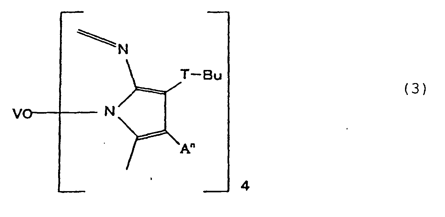
A coating liquid in which a photopolymerization
initiator is added to a multi-functional methacrylate resin
and, further, ITO fine particles (average particle diameter:
10 nm) are dispersed thereto was coated on one major surface
of a triacetyl cellulose (TAC) film (thickness: 80 µm) by a
gravure coater and cured by an ultraviolet ray to form an
electrically conductive hard coat film (film thickness: 3 µm)
and, then, a fluorine-containing organic compound solution
was coated on the thus-formed hard coat film by a micro gravure
coater and dry-cured at 90°C to form an anti-reflection film
(film thickness: 100 nm) having a refractive index of 1.4
whereupon an anti-reflection film 1 was obtained as a
functional transparent layer (E) having a hard coat property
(pencil hardness in accordance with JIS K-5400: 2H), a gas
barrier property (in accordance with ASTM-E96, 1.8 g/m2·day),
an anti-reflection property (Rvis of surface: 1.0%), an
antistatic property (surface resistance: 7 × 10⁹Ω/square)
and an anti-fouling property. An adhesive/a diluting liquid
comprising same raw materials as in the adhesive 1 but not
containing a dye was applied on the other major surface of
the anti-reflection film 1 and, then, dried to form a
transparent adhesive layer (adhesive 2) having a thickness
of 25 µm and, thereafter, a mold releasing film was laminated
on the thus-formed transparent adhesive layer.
A material of a transparent laminate 1/an adhesive 1/a
mold releasing film in roll form was cut into a size of 970
mm × 570 mm and fixed on a supporting plate made of glass such
that a surface of a transparent electrically conductive layer
(D) comes on the top. Further, an anti-reflection film was
laminated only on an inside portion of the transparent
electrically conductive layer (D) while leaving an
electrically conducting portion such that 20 mm wide of a
peripheral portion thereof was exposed by using a laminator.
A plan view as viewed from a surface of the transparent
electrically conductive layer (D) was shown in FIG. 2 as an
example of the electromagnetic wave shielding body according
to the invention. In FIG. 2, a reference numeral 02 denotes
a translucent portion of the electromagnetic wave shielding
body and a reference numeral 03 denotes an electrically
conducting portion of the electromagnetic wave shielding body.
Further, a silver paste (MSP-600F; manufactured by
Mitsui Chemicals, Inc.) was screen-printed to an area of 22
mm wide of a peripheral portion of the transparent electrically
conductive layer (D) such that the silver past covers an exposed
electrically conducting portion and, then, dried to form an
electrode of 15 µm thick. Thereafter, the resultant material
was removed from the supporting plate to prepare the
electromagnetic wave shielding body according to the invention
having a mold releasing film on a surface of the transparent
adhesive layer (C).
Thereafter, the electromagnetic wave shielding body
was deprived of the mold releasing film and was bonded to a
front surface (representation portion: 920 mm × 520 mm) of
a plasma display panel by a sheet fed laminator and, then,
was subjected to an autoclave treatment under heating and
pressure conditions of 60°C and 2 × 10⁵ Pa. An electrode portion
of the electromagnetic wave shielding body and a ground portion
of the plasma display panel were bonded to each other by using
an electrically conductive copper foil adhesive tape (510FR)
manufactured by Teraoka Seisakusho Co., Ltd. to obtain a
display apparatus comprising the electromagnetic wave
shielding body according to the invention. A cross-section
of the electromagnetic wave shielding body is shown in FIG.
3 as an example of the electromagnetic wave shielding body
according to the invention and a mounted state thereof. In
FIG. 3, a reference numeral 00 denotes a display area, a
reference numeral 10 denotes a transparent electrically
conductive layer (D), a reference numeral 20 denotes a polymer
film (B) , a reference numeral 31 denotes a transparent adhesive
layer (C) containing a dye, a reference numeral 40 denotes
a transparent adhesive layer (E), a reference numeral 50
denotes an electrode, a reference numeral 60 denotes a
functional transparent layer (A) having an anti-reflection
property, a hard coat property, a gas barrier property, an
antistatic property and an anti-fouling property, a reference
numeral 61 denotes an anti-reflection film having an
anti-fouling property, a reference numeral 62 denotes a hard
coat film having an antistatic property, a reference numeral
63 denotes a transparent substrate in which the hard coat film
62 and the anti-reflection film 61 are formed and a reference
numeral 80 denotes an electrically conductive copper foil
adhesive tape.
Polyethylene terephthalate pellets 1203 (manufactured
by Unitika, Ltd.) were mixed with 0.01% by weight of a red
color dye PS-Red-G manufactured by Mitsui Chemicals, Inc. for
correcting chromaticity of white color luminescence and 0.015%
by weight of a violet color dye PS-Violet-RC manufactured by
Mitsui Chemicals, Inc., melted at a temperature of from 260°C
to 280°C and extruded to form a film having a thickness of
200 µm. Thereafter, this film was biaxially stretched to
prepare a PET film (polymer film (B) ) containing a dye and having
a thickness of 100 µm.
On one major surface of the PET film, a coating liquid
in which alkoxysilane was decomposed by glacial acetic acid
and added with a silicone type surface smoothing agent was
applied by a gravure coater, and then thermally cured at 120°C
to form a hard coat film (film thickness: 10 µm, pencil
hardness:3H) thereby obtaining a PET film containing a dye
in which a hard coat layer (F) is formed. On the hard coat
layer, a transparent electrically conductive layer (D)
comprising 5 layers in total made up of an SnO2 thin film (film
thickness: 40 nm), a silver thin film (film thickness: 9 nm),
an SnO2 thin film (film thickness: 80 nm), a silver-palladium
alloy thin film (film thickness: 11 nm), and an SnO2 thin film
(film thickness: 40 nm) in this order and having a surface
resistance of 5.3 Ω/square is formed to prepare a transparent
laminate 2 comprising a PET film containing a dye/a hard coat
layer (F)/a transparent electrically conductive layer (D).
An adhesive/a diluting liquid comprising same raw
materials as in the adhesive 1 but not containing a dye was
applied on a surface of PET film of the transparent laminate
2 and, then, dried to form a transparent adhesive layer
(C) (adhesive 3) having a thickness of 25 µm and, thereafter,
a mold releasing film was laminated on the thus-formed
transparent adhesive layer (C).
A material comprising a transparent laminate 2/an
adhesive 3/a mold releasing film in roll form was cut into
a size of 970 mm × 570 mm and fixed on a supporting plate made
of glass such that a surface of a transparent electrically
conductive layer (D) comes on the top.
A coating liquid in which a photopolymerization
initiator is added to a multi-functional methacrylate resin
and, further, organic silica fine particles (average particle
size: 15 µm) are dispersed thereto was prepared.
The coating liquid was flexo-graphically printed only
on an inside portion of the transparent electrically conductive
layer (D) while leaving an electrically conducting portion
thereof such that 20 mm wide of a peripheral portion thereof
was exposed, and cured by an ultraviolet ray to form an
anti-glare layer as a functional transparent layer (A) having
an anti-glare property (haze value measured by a haze meter:
5%), and a hard coat property (pencil hardness: 2H).
Thereafter, the resultant material was removed from the
supporting plate to prepare the electromagnetic wave shielding
body according to the invention having a mold releasing film
on a surface of the transparent adhesive layer (C).
Thereafter, the electromagnetic wave shielding body
was deprived of the mold releasing film and was bonded to a
front surface (representation portion: 920 mm × 520 mm) of
a plasma display panel by a sheet fed laminator and, then,
was subjected to an autoclave treatment under heating and
pressure conditions of 60°C and 2 × 10⁵ Pa. An electrically
conducting portion of the electromagnetic wave shielding body
and a ground portion of the plasma display panel were connected
to each other by using an electrically conductive copper foil
adhesive tape (510FR) manufactured by Teraoka Seisakusho Co.,
Ltd. to obtain a display apparatus comprising the
electromagnetic wave shielding body according to the
invention.
A cross-section of the electromagnetic wave shielding
body is shown in FIG. 4 as an example of the electromagnetic
wave shielding body according to the invention and a mounted
state thereof. In FIG. 4, a reference numeral 00 denotes a
display area, a reference numeral 10 denotes a transparent
electrically conductive layer (D), a reference numeral 21
denotes a polymer film (B) containing a dye, a reference numeral
22 denotes a hard coat layer (F) , a reference numeral 30 denotes
a transparent adhesive layer (C), a reference numeral 70
denotes an anti-glare layer (a functional transparent layer
(E) having an anti-glare property and a hard coat property),
and a reference numeral 80 denotes an electrically conductive
copper foil adhesive tape.
In the same manner as in Example 1, a laminate comprising
a polymer film (B) /a transparent electrically conductive layer
(D) was prepared.
Further, on a major surface of the PET film/transparent
electrically conductive layer wound in roll form, opposite
to a PET film thereof, a next functional transparent layer
1 was continuously formed as a functional transparent layer
(A) by a roll-to-roll method. Namely, a coating liquid in
which a photopolymerization initiator was added to a
multi-functional methacrylate resin and, further, ITO fine
particles (average particlediameter: 10 nm) were added thereto
was applied by a gravure coater and, then, cured by an
ultraviolet ray to form an electrically conductive hard coat
film (film thickness: 3 µm) and, then, a fluorine-containing
organic compound solution was coated on the thus-formed hard
coat film by a micro gravure coater and dry-cured at 90°C to
form an anti-reflection film (film thickness: 100 nm) having
a refractive index of 1.4 thereby forming a functional
transparent layer (A) having a hard coat property (pencil
hardness in accordance with JIS K5400: 2H), an anti-reflection
property (Rvis of surface: 0.9%), an antistatic property
(surface resistance: 7 × 10⁹ Ω/square), and an anti-fouling
property. The a functional transparent layer (A)/a polymer
film (B)/a transparent electrically conductive layer (D) in
roll form was cut into a size of 970 mm × 570 mm and fixed
on a supporting plate made of glass such that the transparent
electrically conductive layer (B) comes to the top. An organic
dye was disperse-dissolved in a solvent of ethyl
acetate/toluene (50:50 wt%) to prepare a diluting liquid for
an acrylic adhesive. The acrylic adhesive/the diluting
liquid containing a dye (80:20wt%) were mixed and the resultant
mixture was applied on the transparent electrically conductive
layer (D) except for 22 mm wide of a peripheral portion thereof
with a film thickness of 25 µm on a dry basis by a batch type
die coater and, then, dried to form an adhesive 1 as the
transparent adhesive layer (C). Further, a refractive index
of the adhesive 1 was 1.51 and an extinction coefficient was
0.
As organic dyes, a dye PD-319 manufactured by Mitsui
Chemicals, Inc. having an absorption maximum in a wavelength
of 595 nm for absorbing an unnecessary luminescence irradiated
from a plasma display and a red color dye PS-Red-G manufactured
by Mitsui Chemicals, Inc. for correcting chromaticity of white
color luminescence were used to adjust the acrylic adhesive/the
dye-containing diluting liquid such that these dyes are
contained in a dried adhesive 1 in amounts of 1150 (wt) ppm
and 1050 (wt) ppm, respectively. Further, PD-319 is a
tetra-t-butyl-tetraazaporphyrin/vanadyl complex expressed
by the following formula (3):

Further, a two-component type room temperature setting
adhesive (3381; manufactured by Three Bond Co., Ltd.) was
printed to an area of 22 mm wide of a peripheral portion of
the transparent electrically conductive layer (D) by using
a metal mask such that an exposed electrically conducting
portion of the transparent electrically conductive layer (D)
is covered and, then, dried to form an electrically conductive
adhesive layer having a thickness of 25 µm.
After the thus-formed electrically conductive
adhesive layer was removed from a supporting body, a mold
releasing film was laminated to each of the transparent
adhesive layer (C) and electrically conductive adhesive
surfaces to prepare an electromagnetic wave shielding body
according to the invention having a mold releasing film on
one surface thereof.
Further, after being deprived of the mold releasing
film, the electromagnetic wave shielding body was bonded to
a front surface (representation portion: 920 mm × 520 mm) of
a plasma display panel by using a sheet fed laminator. On
this occasion, bonding operations of the transparent adhesive
layer (C) portion and the electrically conductive adhesive
layer were performed such that they were in registry with at
least the representation portion and at least a ground portion,
respectively. After such bonding operations, the resultant
plasma display panel was subjected to an autoclave treatment
under heat and pressure conditions of 60°C and 2 × 10⁵ Pa to
obtain a display apparatus comprising the electromagnetic wave
shielding body according to the invention.
A plane as viewed from a side of a transparent adhesive
layer of the electromagnetic wave shielding body is shown in
FIG. 5 as a plan view showing an example of the electromagnetic
wave shielding body according to the invention. In FIG. 5,
a reference numeral 31 denotes a transparent adhesive layer
(C) containing a dye and a reference numeral 41 denotes an
electrically conductive adhesive layer.
A cross-section of the electromagnetic wave shielding
body is shown in FIG. 6 as a cross-sectional diagram showing
an example of the electromagnetic wave shielding body according
to the invention and a mounted state thereof. In FIG. 6, a
reference numeral 00 denotes a display area, a reference
numeral 10 denotes a transparent electrically conductive layer
(D), a reference numeral 20 denotes a polymer film (B), a
reference numeral 31 denotes a transparent adhesive layer (C)
containing a dye, a reference numeral 41 denotes an
electrically conductive adhesive layer, a reference numeral
60 denotes a functional transparent layer (A) having an
anti-reflection property, a hard coat property, an antistatic
property and an anti-fouling property, a reference numeral
61 denotes an anti-reflection film having an anti-fouling
property, and a reference numeral 62 denotes a hard coat film
having an antistatic property.
A polymer film (B) was prepared in the same manner as
in Example 3.
Polyethylene terephthalate pellets 1203 (manufactured
by Unitika, Ltd.) were mixed with 0.01% by weight of a red
color dye PS-Red-G manufactured by Mitsui Chemicals, Inc. for
correcting chromaticity of white color luminescence and 0.015%
by weight of a violet color dye PS-Violet-RC manufactured by
Mitsui Chemicals, Inc., melted at a temperature of from 260°C
to 280°C and extruded to form a film having a thickness of
200 µm. Thereafter, this film was biaxially stretched to
prepare a PET film which contains a dye and is a polymer film(B)
containing a dye and having a thickness of 100 µm.
On one major surface of the PET film, a transparent
electrically conductive layer (D) comprising 5 layers in total
made up of an SnO2 thin film (film thickness: 40 nm), a silver
thin film (film thickness: 9 nm), an SnO2 thin film (film
thickness: 80 nm), a silver-palladium alloy thin film (film
thickness: 11 nm), and an SnO2 thin film (film thickness: 40
nm) in this order and having a surface resistance of 5.3
Ω/square is formed to prepare a transparent laminate 2
comprising a PET film containing a dye/ a transparent
electrically conductive layer (D) by a roll-to-roll method.
Further, on a major surface of the PET film/the
transparent electrically conductive layer wound in roll form,
opposite to the PET film thereof, a next functional transparent
film 2 was continuously formed as a functional transparent
layer (A) by a roll-to-roll method. A coating liquid in which
a photopolymerization initiator was added to a
multi-functional methacrylate resin and, further, organic
silica fine particles (average particle diameter: 15 µm) were
dispersed therein was prepared, applied and, then, cured by
an ultraviolet ray to form an anti-glare layer as a functional
transparent layer (A) having an anti-glare property (haze value
measured by a haze meter: 5%), a hard coat property (pencil
hardness: 2H).
The functional transparent layer (A)/a polymer film
(B)/a transparent electrically conductive layer (D) in roll
form was cut into a size of 970 mm × 570 mm and fixed on a
supporting plate made of glass such that the transparent
electrically conductive layer (D) comes to the top.
An adhesive 2 comprising same raw materials as in the
adhesive 1 in Example 1 except that a dye was not contained
was formed on a mold releasing film surface in a thickness
of 25 µm. The adhesive 2/the mold releasing film was laminated
on the transparent electrically conductive layer while leaving
20 mm wide of a peripheral portion thereof unlaminated by using
a frame-bonding laminator such that a surface of the adhesive
2 is a surface to be bonded. Further, after the mold releasing
film was removed from one side thereof, an electrically
conductive double-faced adhesive tape (WMFT791; manufactured
by Teraoka Seisakusho Co., Ltd.) was bonded to an area of 20
mm wide of the peripheral portion thereof such that an exposed
electrically conducting portion of the transparent
electrically conductive layer (D) was covered.
By being removed from the supporting body, the
electromagnetic wave shielding body according to the invention
having a mold releasing film on one side thereof was prepared.
Further, the electromagnetic wave shielding body was deprived
of the mold releasing film and, then, bonded to a front surface
(representation portion: 920 mm × 520 mm) of a plasma display
panel by a sheet fed laminator. On this occasion, bonding
operations of the transparent adhesive layer (C) portion and
the electrically conductive adhesive layer were performed such
that they were in registry with at least the representation
portion and at least a ground portion, respectively. After
such bonding operations, the resultant plasma display panel
was subjected to an autoclave treatment under heat and pressure
conditions of 60°C and 2 × 10⁵ Pa to obtain a display apparatus
comprising the electromagnetic wave shielding body according
to the invention.
A cross-section of the electromagnetic wave shielding
body is shown in FIG. 7 as a cross-sectional diagram showing
an example of the electromagnetic wave shielding body according
to the invention and a mounted state thereof. In FIG. 7, a
reference numeral 00 denotes a display area, a reference
numeral 10 denotes a transparent electrically conductive layer
(D), a reference numeral 21 denotes a polymer film (B)
containing a dye, a reference numeral 30 denotes a transparent
adhesive layer (C), a reference numeral 41 denotes an
electrically conductive adhesive layer, and a reference
numeral 70 denotes an anti-glare layer (a functional
transparent layer (E) having an anti-glare property and a hard
coat property).
On a major surface of a PET film (thickness: 188 µm)
as a polymer film (B), a transparent electrically conductive
layer having a surface resistance of 15 Ω/square and comprising
an ITO thin film (film thickness: 400 nm) is formed to prepare
a transparent laminate 3. By using the transparent laminate
3, an electromagnetic wave shielding body is prepared in the
same manner as in Example 1 except that a dye is not used to
obtain a display apparatus comprising the thus-prepared
electromagnetic wave shielding body.
The thus-obtained plasma displays which are display
apparatuss each comprising the electromagnetic wave shielding
body according to invention in Examples 1 to 4 were evaluated
according to procedures described below.
By using a CRT color analyzer (CA100) manufactured by
Minolta Co., Ltd., spectral radiance of a plasma display in
each case of before and after an electromagnetic wave shielding
body was formed therein was determined; a ratio of radiance
after the electromagnetic wave shielding body was formed
therein against radiance before the electromagnetic wave
shielding body was formed therein was shown in percentage.
An evaluation was conducted in each case of before and
after an electromagnetic wave shielding body was formed. At
a bright time of about 100 lx of an environmental luminance,
with regard to a plasma display panel, a maximum luminance
(cd/m2) at a time of white color display and a minimum luminance
(cd/m2) at a time of black color display were measured by using
a luminance meter (LS-110) manufactured by Minolta Co., Ltd.
to determine a ratio (maximum luminance/minimum luminance)
therebetween.
An evaluation was conducted in each case of before and
after an electromagnetic wave shielding body was formed.
Measurements were conducted in both cases in which a display
filter was not mounted to the plasma display and the display
filter in Examples 1 and 2 was mounted thereto.
In a white color (W) display, a red color (R) display,
a green color (G) display, and a blue color (B) display, RGB
chromaticity (x, y), white color chromaticity, a white color
temperature and a white color deviation from a black body locus
were measured by using a CRT color analyzer (CA100)
manufactured by Minolta Co., Ltd.
It is preferable that three primary colors of PDP
luminescence comes as near as possible to a color reproduction
gamut of RGB colors defined by an NTSC system. Further, it
is shown that, as a ratio in percentage of an area of a triangle
formed by connecting three primary colors of the PDP
luminescence in an x-y chromaticity diagram against an area
of the color reproduction gamut of NTSC comes nearer to 100%,
the color reproduction gamut becomes larger.
With regard to a plasma display in which an
electromagnetic wave shielding body is not formed and plasma
displays shown in Examples 1 to 4 and Comparative Example 1
in each of which an electromagnetic wave shielding body is
disposed, measurements described below were conducted.
A dipole antenna was placed at a position 10 m away
from a center of a representation portion in a perpendicular
direction. Then, using a spectrum analyzer (TP4172)
manufactured by Advantest Corporation, a radiation field
intensity in a frequency band of from 30 MHz to 230 MHz was
measured. According to a 3-m method of the VCCI, allowable
values in this frequency band are 50 dBµV/m or less in Class
A and 40 dBµV/m or less in Class B. Evaluation was conducted
in 33 MHz and 90 MHz.
Evaluation was conducted on electromagnetic wave
shielding bodies in Examples 1 to 4 and Comparative Example
1.
A small piece was cut out of a translucent portion of
each of the electromagnetic wave shielding bodies, and parallel
light ray transmittance thereof in a wavelength region of from
800 to 1,000 nm was measured by using a spectrophotometer
(U-3400) manufactured by Hitachi, Ltd. Respective
transmittance in wavelengths of 820 nm, 850 nm and 950 nm were
evaluated.
With regard to a plasma display in which an
electromagnetic wave shielding body is not formed and plasma
displays shown in Examples 1 and 2 and Comparative Example
1 in each of which an electromagnetic wave shielding body is
disposed, measurements described below were conducted.
A domestic-use VTR as an electronic apparatus using
an infrared remote controller was placed from 0.2 m to 5 m
away from the plasma display and examined for malfunction
thereof. When the malfunction was observed, a critical
distance for the malfunction was measured. From a practical
point of view, it is at least 3 m or less, and preferably 1.5
m or less.
In the electromagnetic wave shielding body according
to the invention in Example 1, transmittance of light emitted
from the plasma display is 50% in terms of visible light ray
transmittance, and, due to an employment of a dye having an
absorption maximum in a wavelength of 595 nm in which an unwanted
luminescence exists, a percentage of transmittance in a
wavelength of 595 nm against transmittance in a wavelength
of 610 nm in which a necessary luminescence exists was 38%.
Further, in the plasma display comprising such a
electromagnetic wave shielding body, due to an employment of
the electromagnetic wave shielding body in which a functional
transparent layer (A) having an anti-reflection property was
formed, reflection on a display surface was suppressed and,
due to transmission characteristics of the electromagnetic
wave shielding body, contrast ratio in a bright place under
a condition of an environmental luminance of 100 lx was enhanced
to be 45 compared with 20 before the electromagnetic wave
shielding body was formed therein. Further, since a mirror
phenomenon scarcely occurred, a plasma display having a
favorable visibility was obtained.
In the electromagnetic wave shielding body according
to the invention in Example 2, transmittance of light emitted
from the plasma display was 58% in terms of visible light ray
transmittance and a mirror phenomenon scarcely occurred
whereupon a plasma display having a favorable visibility was
obtained. Contrast ratio in a bright place was improved from
20 into 37.
In the electromagnetic wave shielding body according
to the invention in Example 3, transmittance of light emitted
from the plasma display was 58% in terms of visible light ray
transmittance and a mirror phenomenon scarcely occurred
whereupon a plasma display having a favorable visibility was
obtained. Contrast ratio in a bright place was improved from
20 into 37.
In the electromagnetic wave shielding body according
to the invention in Example 4, transmittance of light emitted
from the plasma display was 59% in terms of visible light ray
transmittance and a mirror phenomenon scarcely occurred
whereupon a plasma display having a favorable visibility was
obtained. Contrast ratio in a bright place was improved from
20 into 37.
In FIG. 8, an x-y chromaticity diagram showing color
reproduction gamut in each case of before and after the
electromagnetic wave shielding body was formed was shown. In
FIG. 8, chromaticity of each luminescence of white color (W) ,
red color (R), green color (G), and blue color (B) before and
after the electromagnetic wave shielding body according to
the invention in Example 1 was formed on the PDP (plasma display
panel) was plotted in the x-y chromaticity diagram.
Concurrently, chromaticity of NTSC to be targeted was also
plotted.
White color can be evaluated by comparing a position
thereof with a black body locus which is a locus of a favorable
white color chromaticity.
It has been found that, when the electromagnetic wave
shielding body according to the invention was employed,
chromaticity deviation of white color was small and, further,
a color temperature was in a higher position than that before
the electromagnetic wave shielding body in Example 1 was formed.
On this occasion, the color temperature was elevated from about
7000 K to about 10000 K.
Further, a triangle formed by connecting points of RGB
was shown in FIG. 8. It can be said to be preferable to allow
the triangle to come as near as possible to that of NTSC. It
has been found that, by using the electromagnetic wave
shielding body in Example 1, chromaticity of each of red color
and green color came near to that indicated by NTSC whereupon
a triangle showing a color reproduction gamut became larger.
When a percentage of an area of the triangle indicated by NTSC
against an area of the triangle was obtained, the percentage
was improved to be 85% by forming the electromagnetic wave
shielding body in Example 1 whereas the percentage was 74%
before the electromagnetic wave shielding body in Example 1
was formed.
Results of the evaluations 4) to 6) are summarized and
shown in Table 1.
| Electromagnetic wave shielding body | None | Example 1 | Example 2 | Example 3 | Example 4 | Comparative Example 1 | |
| Surface resistance of transparent electrically conductive layer Ω/square | - | 2.2 | 5.3 | 2.2 | 5.3 | 15 | |
| Radiation field intensity dBµ/m | 33 MHz | 59 | 38 | 46 | 39 | 46 | 52 |
| 90 MHz | 52 | 34 | 42 | 33 | 40 | 49 | |
| Nearinfrared transmittance % | 820 nm | - | 9.8 | 24 | 10 | 25 | 79 |
| 850 nm | - | 6.3 | 19 | 6.5 | 18 | 78 | |
| 950 nm | - | 2.1 | 9 | 2.0 | 8.5 | 70 | |
| Critical distance of | 5 or more | 0.5 | 3.0 | 0.5 | 3.0 | 5 or more |
From Table 1, by using the electromagnetic wave
shielding body according to the invention, it can be seen that
Class B or Class A of VCCI specifications is satisfied. As
the surface resistance of the transparent electrically
conductive layer was lower, the electromagnetic wave shielding
capacity was superior.
Further, by using the electromagnetic wave shielding
body according to the invention, it can be seen that the
near-infrared cutting-off capacity was superior. The
electromagnetic wave shielding body according to the invention
using a transparent electrically conductive layer in which
a metallic thin film and a high- refractive-index transparent
thin film are laminated alternately had low of a near-infrared
ray transmittance, was excellent in near-infrared cutting-off
capacity whereupon, as a surface resistance of the transparent
electrically conductive layer is lower, the near-infrared
cutting-off capacity was excellent. Furthermore, by allowing
the functional transparent layer (D) to have various types
of functions, the electromagnetic wave shielding body
according to the invention is excellent in environmental
resistance and/or scratch resistance and/or an anti-fouling
property and/or an antistatic property.
On one major surface of a triacetyl cellulose (TAC)
film (thickness: 80µm) which is used as a polymer film (B),
a next functional transparent film 1 as described below which
is used as a functional transparent layer (A) was continuously
formed by a roll-to-roll method. Namely, firstly a
multi-functional methacrylate resin was added with a
photopolymerization initiator and, then, coated with a coating
liquid in which ITO fine particles (average particle diameter:
10 nm) were dispersed by means of a gravure coater and cured
by an ultraviolet ray to form an electric conductive hard coat
film (film thickness: 3 µm) and, thereafter, a
fluorine-containing organic compound solution was applied on
the thus-formed electric conductive hard coat film by means
of a micro gravure coater and heat-cured at 90°C to form an
anti-reflection film (film thickness: 100 nm) having a
refractive index of 1.4 thereby forming the functional
transparent film 1 having a hard coat property (pencil hardness
in accordance with JIS K5400:2H), an anti-reflection property
(Rvis of surface:0.9%), an antistatic property (surface
resistance: 7 × 10⁹ Ω/square) and an anti-fouling property.
An organic dye was disperse-dissolved in an ethyl
acetate/toluene (50:50 wt%) solvent to prepare a diluting
liquid for an acrylic adhesive. The acrylic adhesive and the
resultant dye-containing diluting liquid (80:20 wt%) were
mixed and, then, the resultant mixture was applied in a
thickness of 25 µm on a dry basis on a surface of a TAC film
of an functional transparent film 1/a TAC film by means of
a comma coater to form an adhesive 1 as a transparent adhesive
layer (C) . The mold releasing film was laminated to a surface
of the transparent adhesive layer, and then, the resultant
transparent adhesive layer was wound in roll form to obtain
the light control film according to the invention in roll form
having a mold releasing film on the surface of the transparent
adhesive layer.
As an organic dye, a dye PD-319 manufactured by Mitsui
Chemicals, Inc. having an absorption maximum in a wavelength
of 595 nm for absorbing an unnecessary luminescence emitted
from a plasma display and a red color dye PS-Red-G manufactured
by Mitsui Chemicals, Inc. for correcting chromaticity of white
color luminescence were used to adjust the acrylic adhesive/the
dye-containing diluting liquid such that these dyes were
contained in the dried adhesive 1 in amounts of 1650 (wt)ppm
and 450 (wt)ppm, respectively. Further, PD-319 is a
tetra-t-butyl-tetraazaporphyrin/vanadyl complex expressed
by the following formula (3):
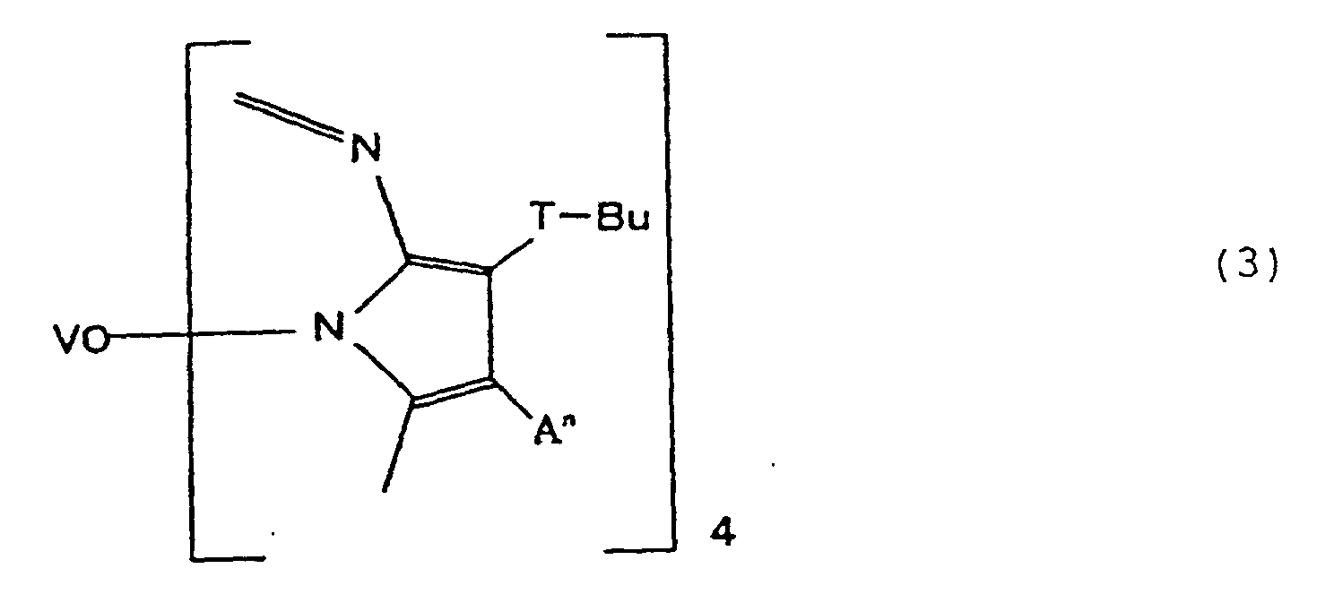
Further, the light control film was cut into sheet form
and, then, the mold releasing film was removed therefrom and,
thereafter, the resultant light control film was bonded to
a front surface of a plasma display panel (representation
portion: 920 mm × 520 mm) by using a sheet fed laminator. On
this occasion, such sheet cutting and registry of a position
to be bonded were conducted such that the transparent adhesive
layer (C) portion was allowed to be bonded to at least an entire
representation portion. After such a bonding operation has
been conducted, the resultant plasma display panel bonded with
the light controlling sheet was subjected to an autoclave
treatment under pressure and heating conditions of 2 × 10⁵
Pa and 60°C to obtain a display apparatus comprising the light
control film according to the invention.
A cross-section of the light control film was shown
in FIG. 9 as a cross-sectional diagram showing an example of
the light control film according to the invention and a mounted
state thereof. In FIG. 9, a reference numeral 00 denotes a
display area, a reference numeral 20 denotes a polymer film
(B), a reference numeral 31 denotes a transparent adhesive
layer (C) containing a dye, a reference numeral 60 denotes
a functional transparent layer (A) having an anti-reflection
property, a hard coat property, an antistatic property, an
anti-fouling property, a reference numeral 61 denotes an
anti-reflection film having an anti-fouling property, and a
reference numeral 62 denotes a hard coat film having an
antistatic property.
Polyethylene terephthalate (PET) pellets 1203
(manufactured by Unitika, Ltd.) were mixed with 0.018% by
weight of a dye PD-319 manufactured by Mitsui Chemicals, Inc.
expressed by the formula (3), 0.018% by weight of a dye PD-311
manufactured by Mitsui Chemicals, Inc. having an absorption
maximum in a wavelength of 585 nm, and 0.004% by weight of
a red dye PS-Red-G manufactured by Mitsui Chemicals, Inc. for
correcting chromaticity of white color luminescence, melted
at a temperature of from 260°C to 280°C and extruded to form
a film having a thickness of 250 µm. Thereafter, this film
was biaxially stretched to prepare a PET film containing a
dye, which is a polymer film (B) containing a dye, having a
thickness of 125 µm.
Further, PD-311 is a
tetra-t-butyl-tetraazaporphyrin/copper complex expressed by
the following formula (4):
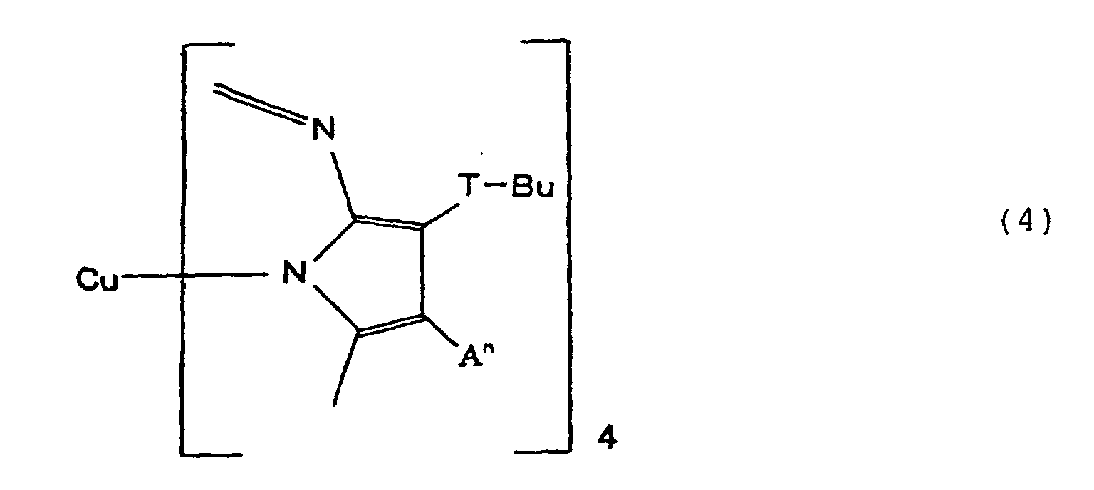
Further, on a major surface of the PET film wound in
roll form, a next functional transparent film 2 was
continuously formed as a functional transparent layer (A) by
a roll-to-roll method. Namely, a coating liquid which had
been prepared by adding a photopolymerization initiator to
a multi-functional methacrylate resin and, further,
dispersing organic silica fine particles (average particle
diameter: 15 µm) therein was applied and, then, cured by an
ultraviolet ray to form a functional transparent film 2, which
is an anti-glare layer, having an anti-glare property (haze
value measured by a haze meter: 5%), a hard coat property (pencil
hardness: 2H). An adhesive 2 comprising same raw materials
as in the adhesive 1 in Example 1 except that a dye was not
contained was formed on a surface of the PET film of the
functional transparent film 2/the dye-containing PET film.
The mold releasing film was laminated on a surface of the
transparent adhesive layer and, then, the resultant
transparent adhesive layer was wound in roll form to obtain
the light control film according to the invention in roll form
having a mold releasing film on the surface of the transparent
adhesive layer thereof.
Further, the light control film was cut into sheet form
and, then, the mold releasing film was removed therefrom and,
thereafter, the resultant light control film was bonded to
a front surface of a plasma display panel (representation
portion: 920 mm × 520 mm) by using a sheet fed laminator. On
this occasion, such sheet cutting and registry of a position
to be bonded were conducted such that the transparent adhesive
layer (C) portion was allowed to be bonded to at least an entire
representation portion. After such a bonding operation has
been conducted, the resultant plasma display panel bonded with
the light controlling sheet was subjected to an autoclave
treatment under pressure and heating conditions of 2 × 10⁵
Pa and 60°C to obtain a display apparatus comprising the light
control film according to the invention.
A cross-section of the light control film was shown
in FIG. 10 as a cross-sectional diagram showing an example
of the light control film according to the invention and a
mounted state thereof. In FIG. 10, a reference numeral 00
denotes a display area, a reference numeral 21 denotes a
transparent adhesive layer (C) containing a dye, a reference
numeral 30 denotes a transparent adhesive layer (C), a
reference numeral 70 denotes an anti-glare layer (a functional
transparent layer (A) having an anti-glare property, and a
hard coat property).
The thus-obtained plasma displays which are display
apparatuses each comprising the light control film according
to the invention in Examples 5 and 6, as well as the plasma
display before the light control film was formed thereon, were
evaluated according to procedures described below.
By using a CRT color analyzer (CA100) manufactured by
Minolta Co., Ltd., spectral radiance of a plasma display in
each case of before and after a light control film was formed
therein was determined; a ratio of radiance after the light
control film was formed therein against radiance before the
light control film was formed therein was shown in percentage.
An evaluation was conducted in each case of before and
after a light control film was formed. At a bright time of
about 100 lx of an environmental luminance, a maximum luminance
(cd/m2) at a time of white color display and a minimum luminance
(cd/m2) at a time of black color display of a plasma display
panel were measured by using a luminance meter (LS-110)
manufactured by Minolta Co., Ltd. to determine a ratio (maximum
luminance/minimum luminance) therebetween.
An evaluation was conducted in each case of before and
after a light control film was formed.
In a white color (W) display, a red color (R) display,
a green color (G) display, and a blue color (B) display, RGB
chromaticity (x, y), white color chromaticity, a white color
temperature and a white color deviation from a black body locus
were measured by using a CRT color analyzer (CA100)
manufactured by Minolta Co., Ltd.
It is preferable that three primary colors of PDP
luminescence comes as near as possible to a color reproduction
gamut of RGB colors defined by an NTSC system. Further, it
is shown that, as a ratio in percentage of an area of a triangle
formed by connecting three primary colors of the PDP
luminescence in an x-y chromaticity diagram against an area
of the color reproduction gamut of NTSC comes nearer to 100%,
the color reproduction gamut becomes larger.
In the light control film according to the invention
in Example 5, transmittance of light emitted from the plasma
display is 69% in terms of visible light ray transmittance,
and, due to an employment of a dye having an absorption maximum
in a wavelength of 595 nm in which an unwanted luminescence
exists, a percentage of transmittance in a wavelength of 595
nm against transmittance in a wavelength of 610 nm in which
a necessary luminescence exists was 21%. Further, in the
plasma display comprising such a light control film, due to
an employment of the light control film in which a functional
transparent layer (A) having an anti-reflection property was
formed, reflection on a display surface was suppressed and,
due to transmission characteristics of the light control film,
contrast ratio in a bright place under a condition of an
environmental luminance of 100 lx was enhanced to be 41 compared
with 20 before the light control film was formed therein.
Further, since luminance was not substantially impaired and
a mirror phenomenon scarcely occurred, a plasma display having
a favorable visibility was obtained. Moreover, color purity
of red color luminescence and green color luminescence was
remarkably improved. Such an improvement of the green color
luminescence is due to a fact that yellowish green color
luminescence by a dye having an absorption wavelength of 595
nm has been decreased.
In the same manner as above, in the light control film
according to the invention in Example 6, transmittance of light
emitted from the plasma display is 70% in terms of visible
light ray transmittance, and, due to an employment of a dye
having an absorption maximum in a wavelength of 585 nm in which
an unwanted luminescence exists in the same manner as in the
dye having an absorption maximum in a wavelength of 595 nm
in which an unwanted luminescence exists, a percentage of
transmittance in a wavelength of 595 nm against transmittance
in a wavelength of 610 nm in which a necessary luminescence
exists was 30%. Further, in the plasma display comprising
such a light control film, due to transmission characteristics
of the light control film, contrast ratio in a bright place
under a condition of an environmental luminance of 100 lx was
enhanced to be 37 compared with 20 before the light control
film was formed therein. Further, since luminance was not
substantially impaired and a mirror phenomenon scarcely
occurred, a plasma display having a favorable visibility was
obtained. Moreover, color purity of red color luminescence
and green color luminescence was remarkably improved. Such
an improvement of the green color luminescence is due to a
fact that yellowish green color luminescence by dyes having
absorption wavelengths of 595 nm and 585 nm has been decreased.
Particularly, by using the dye having an absorption wavelength
of 585 nm for absorbing short wavelength, such an effect as
described above was conspicuous.
In FIG. 11, an x-y chromaticity diagram showing color
reproduction gamut in each case of before and after the light
control film according to the invention was formed was shown.
In FIG. 11, chromaticity of each luminescence of white
color (W), red color (R), green color (G), and blue color (B)
was plotted in the x-y chromaticity diagram in each case of
before and after the light control film in Example 5 was formed
on the PDP (plasma display panel). Concurrently,
chromaticity of NTSC to be targeted was also plotted.
White color can be evaluated by comparing a position
thereof with a black body locus which is a locus of a favorable
white color chromaticity.
It has been found that, when the electromagnetic wave
shielding body according to the invention was employed,
chromaticity deviation of white color was small and, further,
a color temperature was in a higher position than that before
the light control film in Example 5 or Example 6 was formed.
On this occasion, the color temperature was elevated from about
7000 K to about 9500 K and a white color deviation showing
a deviance from the black body locus was approximately 0.
Further, a triangle formed by connecting points of RGB
was shown in FIG. 11. It can be said to be prefertble to allow
the triangle to come as near as possible to that of NTSC. It
has been found that, by using the light control film in Example
5 or Example 6, chromaticity of each of red color and green
color came near to that indicated by NTSC whereupon a triangle
showing a color reproduction gamut became larger. When a
percentage of an area of the triangle indicated by NTSC against
an area of the triangle was obtained, the percentage was
improved to be 86% by forming the light control film in Example
5 whereas the percentage was 74% before the light control film
in Example 5 was formed. Further, the percentage was improved
to be 88% in the case of forming the light control film in
Example 6.
Furthermore, by allowing the functional transparent
layer (A) to have various types of functions, the light control
film according to the invention is excellent in scratch
resistance and/or an anti-fouling property and/or an
antistatic property.
Polyethylene terephthalate pellets 1203 (manufactured
by Unitika, Ltd.) were mixed with 0.15% by weight of each of
near-infrared absorbing dyes SIR-128 and SIR-130 manufactured
by Mitsui Chemicals Inc., melted at about 280°C, extruded and
biaxially stretched to prepare a near-infrared shielding film
(B) having a thickness of 150 µm. Further, as allowing a
solvent of ethyl acetate/toluene (50:50 wt%) to be a diluting
liquid, an acrylic adhesive and the diluting liquid were mixed
with each other at a mixing ratio of 80:20 and, then, the
resultant mixture was applied on a surface of the near-infrared
shielding film with a film thickness of 25 µm on a dry basis
by means of a comma coater and dried to form an adhesive layer
on which a mold releasing film was thereafter laminated.
On the resultant near-infrared shielding film (B), an
anti-reflection film comprising a base film having the
thickness of 188 µm (under the trade name of "ReaLook 1200";
manufactured by NOF Corporation) was laminated and, then, the
resultant laminate was cut to a size of 960 mm long × 550 mm
wide to obtain an optical filter film comprising a transparent
polymer film having a total thickness of 0.338 mm.
Thus-obtained film was bonded to a semi-tempered glass
plate having a size of 980 long × 580 mm wide × 2.5 mm thick.
Polyethylene terephthalate pellets 1203 (manufactured
by Unitika, Ltd.) were mixed with 0.3% by weight of each of
near-infrared absorbing dyes SIR-128 and SIR-130 manufactured
by Mitsui Chemicals Inc., melted at about 280°C, extruded and
biaxially stretched to prepare a near-infrared shielding film
having a thickness of 75 µm. Further, as allowing a solvent
of ethyl acetate/toluene (50:50 wt%) to be a diluting liquid,
an acrylic adhesive and the diluting liquid were mixed with
each other at a mixing ratio of 80:20 and, then, the resultant
mixture was applied on a surface of the near-infrared shielding
film in a film thickness of 25 µm on a dry basis by means of
a comma coater and dried to form an adhesive layer on which
a mold releasing film was thereafter laminated.
By using a similar method to that described above, a
transparent polymer film for increasing a total thickness
having a thickness of 200 µm was prepared without adding a
near-infrared absorbing dye.
On the resultant near-infrared shielding film, an
ant-reflection film (under the trade name of "ReaLook 2200";
manufactured by NOF Corporation) comprising a base film having
a thickness of 80 µm was laminated and, then, the resultant
laminate was cut to a size of 960 mm long × 550 mm wide and
bonded to the transparent polymer film for increasing a total
thickness having a thickness of 200 µm thereby obtaining an
optical filter film comprising a transparent polymer film
having a total thickness of 0.355 mm. This optical filter
film was bonded to a semi-tempered glass plate having a size
of 980 long × 580 mm wide × 2.5 mm thick.
On a major surface of the near-infrared shielding film
having a thickness of 150 µm as shown in Example 7, a next
functional transparent film was continuously formed as a
functional transparent layer (A) by a roll-to-roll method.
Namely, a coating liquid which had been prepared by adding
a photopolymerization initiator to a multi-functional
methacrylate resin and, further, dispersing organic silica
fine particles (average particle diameter: 15 µm) therein was
applied and, then, cured by an ultraviolet ray to form a
functional transparent layer which has anti-glare capacity
having an anti-glare property (haze value measured by a haze
meter: 5%), a hard coat property (pencil hardness: 2H).
The transparent polymer film for increasing a total
thickness having a thickness of 200 µm as shown in Example
14 was laminated to a transparent polymer film having such
a near-infrared shielding function and an anti-glare function
and cut to a size of 960 mm long × 550 mm wide to obtain an
optical filter film comprising a transparent polymer film
having a total thickness of 0.350 mm. Thus-obtained optical
filter film was bonded to a semi-tempered glass plate having
a size of 980 long × 580 mm wide × 2.5 mm thick.
A polyethylene terephthalate film having a thickness
of 75 µm was prepared by an extrusion and biaxially stretching
operations and, then, on one major surface of the thus-prepared
polyethylene terephthalate film, 5 layers made up of an SnO2
thin film (film thickness: 40 nm), a silver thin film (film
thickness: 9 nm), an SnO2 thin film (film thickness: 80 nm),
a silver-palladium alloy thin film (film thickness: 11 nm),
and an SnO2 thin film (film thickness: 40 nm) were formed in
this order as viewed from the polyethylene terephthalate film
whereupon a transparent polymer film having electromagnetic
wave shielding capacity was prepared in which a transparent
electrically conductive thin film layer (D) having a surface
resistance of 5.3 Ω/square was contained.
An adhesive layer was formed on the electromagnetic
wave shielding film by procedures described below.
An organic dye was disperse-dissolved in a solvent of
ethyl acetate/toluene (50:50wt%) to prepare a diluting liquid
for an acrylic adhesive. As an organic dye, a dye PD-319
manufactured by Mitsui Chemicals, Inc. having an absorption
maximum in a wavelength of 595 nm for absorbing an unnecessary
luminescence emitted from a plasma display and a red color
dye PS-Red-G manufactured by Mitsui Chemicals, Inc. for
correcting chromaticity of white color luminescence were used
to adjust the acrylic adhesive/the dye-containing diluting
liquid such that these dyes were contained in the dried adhesive
in amounts of 1150 (wt)ppm and 1050 (wt)ppm, respectively.
The acrylic adhesive and the resultant dye-containing
diluting liquid were mixed (80:20wt%) and, then, the resultant
mixture was applied in a film thickness of 25 µm on a dry basis
on a surface thereof in side of the electromagnetic wave
shielding film by means of a comma coater, dried and laminated
with a mold releasing film on an adhesive surface thereof to
form a transparent adhesive layer thereon.
The thus-prepared film was laminated on the transparent
polymer film for increasing a total thickness having a
thickness of 200 µm as shown in Example 8 such that the
transparent electrically conductive thin film layer comes to
the top and, then, cut to a size of 960 mm long × 550 mm wide.
Further, ananti-reflection film comprising a base film
having a thickness of 188 µm (ReaLook 1200; manufactured by
NOF Corporation) was cut to a size of 920 mm long × 510 mm
wide and, then, the thus-cut anti-reflection film was bonded
inside the transparent electrically conductive layer such that
20 mm wide of a peripheral portion thereof was exposed.
Furthermore, a silver paste (MSP-600F; manufactured by Mitsui
Chemicals, Inc.) was screen-printed thereon such that an
exposed electrically conducting portion of the transparent
electrically conductive layer was covered in an area of 22
mm wide of the peripheral portion thereof and dried to form
an electrode having a thickness of 15 µm. By this procedure,
an optical filter film comprising a transparent polymer film
having a total thickness of 0.463 mm was obtained. This film
was bonded to a semi-tempered glass plate having a size of
980 long × 580 mm wide × 2.5 mm thick.
A polyethylene terephthalate film having a thickness
of 200 µm was prepared by an extrusion and biaxially stretching
operations and, then, on one major surface of the thus-prepared
polyethylene terephthalate film, a transparent electrically
conductive thin layer (F) comprising 7 layers in total made
up of an ITO thin film (40 nm thick), a silver thin film (11
nm thick), an ITO thin film (95 nm thick), a silver thin film
(14 nm thick), an ITO thin film (90 nm thick) , a silver thin
film (12 nm thick) and an ITO thin film (40 nm thick) in this
order as viewed from a side of the polyethylene terephthalate
film was formed whereupon an electromagnetic wave shielding
film comprising the transparent electrically conductive layer
having a surface resistance of 2.2 Ω/square was prepared.
On the other major surface on which the transparent
electrically conductive thin layer of the thus-prepared
electromagnetic wave shielding film was not formed, a next
functional transparent layer was continuously formed by means
of a roll-to-roll method. Namely, a coating liquid in which
a photopolymerization initiator is added to a multi-functional
methacrylate resin and, further, ITO fine particles (average
particle diameter: 10 nm) were dispersed thereto was coated
by a gravure coater and cured by an ultraviolet ray to form
an electrically conductive hard coat film (film thickness:
3 µm) and, then, a fluorine-containing organic compound
solution was coated on the thus-formed hard coat film by a
micro gravure coater and dry-cured at 90°C to form an
anti-reflection film (film thickness: 100 nm) having a
refractive index of 1.4 whereupon a functional transparent
layer having a hard coat property (pencil hardness in
accordance with JIS K-5400: 2H), an anti-reflection property
(Rvis of surface: 0.9%), an antistatic property (surface
resistance: 7 × 10⁹Ω/square) and an anti-fouling property was
formed.
Further, as allowing a solvent of ethyl acetate/toluene
(50:50 wt%) to be a diluting liquid, an acrylic adhesive and
the diluting liquid were mixed with each other at a mixing
ratio of 80:20 and, then, the resultant mixture was applied
on a surface of the transparent electrically conductive layer
in a film thickness of 25 µm on a dry basis by means of a comma
coater, dried and laminated with a mold releasing film to form
a transparent adhesive layer.
Further, the electromagnetic wave shielding film
having the functional transparent layer was cut to a size of
920 mm long × 510 mm wide and, then, the thus-cut electromagnetic
wave shielding film was bonded to an inside surface of a
transparent polymer film for increasing a total thickness,
which has been cut to a size of 960 mm long × 550 mm wide,
having a thickness of 200 µm such that 20 mm wide each of a
peripheral portion thereof was left.
Furthermore, a silver paste (MSP-600F; manufactured
by Mitsui Chemicals, Inc.) was screen-printed in an area of
22 mm wide of the peripheral portion thereof such that an
electrically conducting portion in a direction of a thickness
cross-section of the transparent electrically conductive
layer was covered, and dried to form an electrode having a
thickness of 15 µm. By this procedure, an optical filter film
comprising a transparent polymer film having a total thickness
of 0.4 mm was obtained. This optical filter film was bonded
to a semi-tempered glass plate having a size of 980 long ×
580 mm wide × 2.5 mm thick.
The near-infrared shielding film having a thickness
of 150 µm as shown in Example 9 and the anti-reflection film
comprising a base film having a thickness of 80 µm were bonded
to each other to obtain an optical filter film having a total
film thickness of 0.230 mm. The thus-obtained optical filter
film was bonded to a semi-tempered glass plate having a size
of 980 long × 580 mm wide × 2.5 mm thick.
The electromagnetic wave shielding film having a
thickness of 75 µm as shown in Example 10 and the anti-reflection
film comprising a base film having a thickness of 188 µm were
bonded to each other to obtain an optical filter film having
a total film thickness of 263 µm. The thus-obtained optical
filter film was bonded to a semi-tempered glass plate having
a size of 980 long × 580 mm wide × 2.5 mm thick.
On samples thus obtained by bonding respective optical
filter films to respective glass plates, an enhancement of
shock resistance, a peeling property, and a state of a remaining
adhesive on a glass plate were examined.
In regard to a shock resistance test, a steel ball having
a weight of 500 g was dropped on a film sample bonded to a
glass plate from 1.5 m high and a state of damage of the substrate
glass was examined. 5 sheets of samples were subjected to
each test.
In regard to tests of the peeling property and paste
remaining on glass, after an optical film was bonded to a glass
plate and left still for one hour and, the film was peeled
off the glass plate to examine a state at the time of such
peeling.
Results thus obtained are shown in Table 2.
| Film total thickness (mm) | Shock resistance test | Film peeling property | Adhesive remaining on glass | |
| Example 9 | 0.338 | No problem | Easy peeling | No |
| Example 10 | 0.355 | No problem | Easy peeling | No |
| Example 11 | 0.350 | No problem | Easy peeling | No |
| Example 12 | 0.413 | No problem | Easy peeling | No |
| Example 13 | 0.400 | No problem | Easy peeling | No |
| Comparative Example 2 | 0.155 | Glass partially flown to reverse surface | Difficult peeling | Yes |
| Comparative Example 3 | 0.263 | Glass partially flown to reverse surface | Difficult peeling | Yes |
As is evident from Table 2, it can be seen that shock
resistance, a peeling property, and a state of paste remaining
on a glass plate have been enhanced in all examples.
As described above, the invention can aim for enhancing
a protection function and workability of a display panel by
allowing a total thickness of a transparent polymer film
constituting an optical filter film to be 0.3 mm or more and
provide the optical filter film capable of being bonded
directly on a front surface of a display.
A roll of a polyethylene terephthalate film (558 mm
wide, 500 m long and 75 µm thick) was prepared as a transparent
polymer film (B) . On one major surface thereof, a transparent
electrically conductive thin film layer (D) was deposited by
a DC magnetron sputtering method by means of a roll coater.
In the transparent electrically conductive thin film layer,
a thin film layer (Dt) comprising an oxide of indium and tin
and a silver thin film layer (Dm) are laminated in an order
of B/Dt (40 nm thick)/Dm (15 nm thick)/Dt (80 nm thick)/Dm
(20 nm thick)/Dt (80 nm thick)/Dm (15 nm thick)/Dt (40 nm
thick)/Dm (15 nm thick)/Dt (40 nm thick). The thin film layer
comprising an oxide of indium and tin constitutes a
high-refractive-index transparent thin film layer while the
silver thin film layer constitutes a metallic thin film layer
comprising silver or a silver alloy. For depositing the thin
film layer comprising the oxide of indium and tin, an indium
oxide/a tin oxide sintered body (In2O3:SnO2 = 90:10 wt%) was
used as a target and an argon-oxygen gaseous mixture (total
pressure of 266 mPa; partial pressure of oxygen of 5 mPa) was
used as a sputtering gas. For depositing a silver thin film
layer, silver was used as a target and an argon gas (total
pressure of 266 mPa) was used as a sputtering gas. For
depositing a titanium layer, titanium was used as a target
and an argon gas (total pressure of 266 mPa) was used as a
sputtering gas.
Next, a roll of an anti-glare film (548 mm wide, 500
m long, 100 µm thick) was prepared in a state in which a
transparent adhesive (100 µm thick) was bonded to a side thereof
opposite to an anti-glare layer.
Subsequently, the thus-prepared anti-glare film was
bonded on a transparent electrically conductive thin film layer
of the transparent electrically conductive thin film via the
transparent adhesive by means of a roll-to-roll method to
prepare one roll. A center position of the transparent
electrically conductive film was allowed to be in registry
with a center position of the anti-glare film in a width
direction. Further, on a surface opposite to the anti-glare
layer of a bonded body made up of the transparent electrically
conductive thin film and the anti-glare film, bonded was a
transparent adhesive (100 µm thick) by a roll-to-roll method.
Subsequently, a silver paste was applied to respective
transparent electrically conductive thin film layer portions
of 5 mm wide of both end parts of the roll by a roll coat method.
On this occasion, a transfer rate of the roll was 0.5 m/s.
The resultant film was cut to a size of 958 mm long
to prepare an electromagnetic wave shielding body. A
cross-sectional diagram thereof was shown in FIG. 12. In FIG.
12, a reference numeral 23 denotes a transparent polymer film
(B) having an electromagnetic wave shielding function, a
reference numeral 30 denotes a transparent adhesive layer (C),
and a reference numeral 24 denotes a transparent polymer film
(B) having a functional transparent layer (A).
A time required for forming an electrode per sheet of
the electromagnetic wave shielding body therein was examined.
Subsequently, the electromagnetic wave shielding body
was at tached to a front face of a plasma display panel (PX-42VP1;
manufactured by NEC Corporation) via the transparent adhesive
layer.
The electrode disposed on a surface facing to a viewer
thereof was allowed to come into contact with a metallic member
on a plate which is wired such that an electric current can
be led to an outside of the display.
After the plasma display panel was actuated, an
intensity of electromagnetic wave discharged externally was
measured in accordance with FCC specifications Part 15J to
examine whether or not the resultant measurements complied
with Class A standards.
A roll of an anti-glare film (554 mm wide, 500 m long
and 100 µm thick) was prepared and, then, a transparent
electrically conductive thin film layer was formed on a surface
opposite to an anti-glare layer thereof in the same manner
as in Example 14. Subsequently, a transparent adhesive (548
mm wide and 100 µm thick) and an electrically conductive
adhesive (3 mm wide and 100 µm thick) were bonded to the
thus-formed transparent electrically conductive thin film
layer by a roll-to-roll method. The electrically conductive
adhesive was bonded to positions of both edge portions of the
roll while the transparent adhesive was bonded to a remaining
portion. By these procedures, an electromagnetic wave
shielding body was prepared.
The electromagnetic wave shielding body was attached
to a front face of a plasma display panel (PX-42VP1;
manufactured by NEC Corporation). On each of 2 long sides
of the plasma display panel, a copper foil tape was previously
bonded along an edge portion thereof by 6 mm wide. An
overlapped portion by the electrically conductive adhesive
and the copper foil tape becomes a substantial electrode. The
electrode positioned in a side of a viewing surface was allowed
to come into contact with a plate type metallic member which
is wired such that an electric current can be led to an outside
of the display. Other arrangements than those described above
are made in the same manner as in Example 14.
A transparent electrically conductive thin film was
prepared in the same manner as in Example 14.
Subsequently, a roll of an anti-glare film (558 mm wide,
500 m long, and 100 µm) was prepared. Center positions of
the transparent electrically conductive thin film and the
anti-glare film were allowed to be in registry with each other
in a width direction. Further, on a surface opposite to the
anti-glare layer of the resultant bonded body made up of the
transparent electrically conductive thin film and the
anti-glare film, bonded was a transparent adhesive (100 µm
thick) by a roll-to-roll method.
A silver paste was applied to an edge portion the roll.
By the above-described procedures, an electromagnetic wave
shielding body was prepared. A cross-sectional diagram was
shown in FIG. 17.
A time required for forming an electrode per sheet of
the electromagnetic wave shielding body therein was examined.
Subsequently, the electromagnetic wave shielding body
was attached to a front face of a plasma display panel (PX-42VP1;
manufactured by NEC Corporation). The electrode disposed was
allowed to come into contact with a plate type metallic member
which is wired such that an electric current can be led to
an outside of the display.
After the plasma display panel was actuated, an
intensity of electromagnetic wave discharged externally was
measured in accordance with FCC specifications Part 15J to
examine whether or not the resultant measurements complied
with Class A standards.
In the same manner as in Example 14, a roll of a
polyethylene terephthalate film (558 mm wide, 500 m long and
75 µm thick) was prepared as a transparent polymer film (B)
and, then, on one major surface thereof, formed was a
transparent electrically conductive thin film layer.
A transparent adhesive (100 µm thick) was bonded to
a surface opposite to a surface of the above-described film
by a roll-to-roll method.
Further, while the resultant film was cut, it was bonded
to a glass substrate (size being 560 mm × 960 mm; thickness
being 3 mm) via an adhesive of weak adhesive strength.
Subsequently, a roll of an anti-glare type film (548
mm wide, 500 m long and 100 µm thick) was prepared in a state
in which a transparent adhesive was bonded to a side opposite
to an anti-glare layer thereof and, then, on the transparent
electrically conductive thin film layer of the above-described
bonded body, the thus-prepared roll was bonded while it was
cut. On this occasion, the thus-cut roll was bonded such that
an edge thereof was positioned 5 mm inside from a peripheral
portion of the transparent electrically conductive thin film
layer.
A silver paste was applied by using a screen printing
method such that an entire exposed portion of the transparent
electrically conductive thin film layer positioned in a
peripheral part thereof was covered and dried. After the
silver paste was dried, the resultant film was removed from
the glass substrate. By the above-described procedures, an
electromagnetic wave shielding body was prepared. The others
were conducted in the same manner as in Example 14.
Results are shown in Table 3.
| Electrode formation time (second) (per sheet of electromagnetic wave shielding body) | Electromagnetic wave shielding effect (whether or not being within FCC Class A standards) | |
| Example 14 | 2 | No problem |
| Example 15 | 2 | No problem |
| Example 16 | 0.5 | No problem |
| Comparative Example 4 | 180 | No problem |
As is evident from Table 3, in all examples, in regard
to the electromagnetic wave shielding effect, there is no
problem in the same manner as in a conventional case as shown
in Comparative Example 4. Further, it can be seen that a time
required for forming the electrode has substantially been
decreased thereby substantially improving production
efficiency.
A roll of a polyethylene terephthalate film (565 mm
wide, 500 m long and 75 µm thick) was prepared as a transparent
polymer film (B). On one major surface thereof, a transparent
electrically conductive layer (D) was deposited by a DC
magnetron sputtering method by means of a roll coater. In
the transparent electrically conductive thin film layer, a
thin film layer (Dt) comprising an oxide of indium and tin
and a silver thin film layer (Dm) are laminated in an order
of B/Dt (40 nm thick)/Dm (15 nm thick)/Dt (80 nm thick)/Dm
(20 nm thick)/Dt (80 nm thick)/Dm (15 nm thick)/Dt (40 nm
thick) /Dm (15 nm thick)/Dt (40 nm thick). The thin film layer
comprising an oxide of indium and tin constitutes a
high-refractive-index transparent thin film layer while the
silver thin film layer constitutes a metallic thin film layer
comprising silver or a silver alloy. For depositing the thin
film layer comprising the oxide of indium and tin, an indium
oxide/a tin oxide sintered body (In2O3:SnO2 = 90:10 wt%) was
used as a target and an argon-oxygen gaseous mixture (total
pressure of 266 mPa; partial pressure of oxygen of 5 mPa) was
used as a sputtering gas. For depositing a silver thin film
layer, silver was used as a target and an argon gas (total
pressure of 266 mPa) was used as a sputtering gas. For
depositing a titanium layer, titanium was used as a target
and an argon gas (total pressure of 266 mPa) was used as a
sputtering gas.
Next, a roll of an anti-glare film having a width of
565 mm and a length of 500 m was prepared in a state in which
a transparent adhesive was bonded to a side thereof opposite
to an anti-glare layer.
Subsequently, the thus-prepared anti-glare film was
bonded on a transparent electrically conductive thin film layer
of the transparent electrically conductive thin film via the
transparent adhesive by a roll-to-roll method to prepare one
roll. Further, on a surface opposite to the anti-glare layer
of the resultant bonded body made up of the transparent
electrically conductive thin film and the anti-glare film,
bonded was a transparent adhesive by a roll-to-roll method.
Further, while the resultant film was cut, it was bonded
to a transparent supporting substrate via a transparent
adhesive.
Further, a silver paste was applied to an entire
periphery of an edge portion of the film by using a screen
printing method such that a side surface thereof was covered
and, then, dried.
By the above-described procedures, an electromagnetic
wave shielding body was prepared. A cross-sectional diagram
was shown in FIG. 16.
2 points on the electrode which are remotest from each
other were selected and, then, resistance therebetween was
examined.
Further, a bonding time required for every sheet of
the electromagnetic wave shielding body was examined.
Furthermore, a bonding time required for every sheet of an
optical filter comprising the transparent electrically
conductive film and the anti-glare film was determined by
dividing a total bonding time required for total roll-to-roll
methods employed by a number of sheets of film which can be
cut out of the roll.
A roll of an anti-glare film having a width of 565 mm
and a length of 500 m was prepared and, then, a transparent
electrically conductive thin film layer was formed on a surface
opposite to an anti-glare layer thereof in the same manner
as in Example 17. Subsequently, a transparent adhesive was
bonded on the transparent electrically conductive thin film
layer by a roll-to-roll method.
While the thus-obtained film was being cut, it was
bonded to a transparent supporting substrate via the
transparent adhesive.
Further, a silver paste was applied to an entire
periphery of an edge portion of the film such that a side surface
thereof is covered by a screen printing method and, then, dried.
By the above-described procedures, an electromagnetic wave
shielding body was prepared. A cross-sectional diagram
thereof was shown in FIG. 17.
On this occasion, 2 points on the electrode which are
remotest from each other were selected and, then, resistance
therebetween was examined.
Further, a bonding time required for every sheet of
the electromagnetic wave shielding body was examined.
A roll of an anti-glare film having a width of 565 mm
and a length of 500 m was prepared and, then, a transparent
electrically conductive thin film layer was formed on a surface
opposite to an anti-glare layer thereof in the same manner
as in Example 17 to prepare a roll of an anti-glare transparent
electrically conductive film having a length of 500 m.
2 rolls of copper tapes (each being 15 mm wide, 75 µm
thick and 500 m long; electrically conductive adhesive being
attached to one side thereof) were prepared.
A copper tape was bonded to each of both edge portions
of the anti-glare transparent electrically conductive film.
A bonding operation was conducted such that a transparent
electrically conductive layer formed as having an anti-glare
transparent electrically conductive property came into
contact with the electrically conductive adhesive of the copper
tape. Further, an overlapping width between each copper tape
and the anti-glare transparent electrically conductive film
was allowed to be 10 mm. Bonding therebetween was conducted
by a roll-to-roll method.
A roll of a transparent adhesive (575 mm wide, 25 µm
thick and 500 m long) was prepared. The thus-prepared
transparent adhesive was bonded on an anti-glare transparent
electrically conductive film with a side face being bonded
with a copper tape and, then, while keeping such a configuration,
the resultant film was further cut out to be a sheet having
a length of 958 mm and, thereafter, on a side on which the
transparent electrically conductive layer and the copper tape
had not been bonded of the thus-cut out sheet, an adhesive
was allowed to be bonded. On this occasion, a bonding operation
was conducted by a roll-to-roll method. By the
above-described procedures, an electromagnetic wave
shielding body was prepared. A cross-section thereof was
shown in FIG. 24.
On this occasion, 2 points on the electrode which are
remotest from each other were selected and, then, resistance
therebetween was examined.
Further, a bonding time required for every sheet of
the electromagnetic wave shielding body was examined.
A roll of an anti-glare film having a width of 565 mm
and a length of 500 m was prepared and, then, on a surface
opposite to an anti-glare layer thereof, formed was a
transparent electrically conductive thin film layer in the
same manner as in Example 17. Subsequently, a transparent
adhesive was bonded on the transparent electrically conductive
thin film layer by a roll-to-roll method and, then, while
keeping such a configuration, the resultant film was further
cut out to be a sheet having a length of 958 mm thereby preparing
an electromagnetic wave shielding body.
A glass substrate (size being 545 mm × 960 mm, thickness
being 3 mm) was prepared and, then, on each of 2 long sides
thereof, disposed was a copper plate (size being 10 mm × 960
mm, thickness being 3 mm). In this copper plate, provided
were screw holes. These screw holes were formed at an interval
of 30 mm in a longitudinal direction across the copper plate
in a range of from one end to the other end thereof. On the
resultant supporting substrate comprising a glass plate and
the copper plate, bonded was an electromagnetic wave shielding
body. Next, screws were fitted to respective screw holes which
had been provided in the copper plate. A screw-fitting
operation was conducted such that each of the screws was allowed
to penetrate the electromagnetic wave shielding body from an
outermost surface thereof. On this occasion, the screw became
a substantial through-hole electrode. By the above-described
procedures, an electromagnetic wave shielding body was
prepared. A cross-sectional diagram was shown in FIG. 25.
On this occasion, 2 points on the electrode which are
remotest from each other were selected and, then, resistance
therebetween was examined.
Further, a bonding time required for every sheet of
the electromagnetic wave shielding body was examined.
A roll having a width of 565 mm and a length of 500
m of a polyethylene terephthalate film (75 µm thick) was
prepared as a transparent polymer film (B). On one major
surface thereof, a transparent electrically conductive thin
film layer was formed.
On a surface of the above-described film that is
opposite to a surface on which the transparent electrically
conductive thin film was formed, a transparent adhesive was
bonded by a roll-to-roll method.
Further, while the resultant film was being cut, the
thus-cut film was bonded to a transparent supporting substrate
via the transparent adhesive.
Subsequently, a roll of an anti-glare film having a
width of 565 mm and a length of 500 m was prepared in a state
in which a transparent adhesive was bonded on a side opposite
to an anti-glare layer and, then, while the resultant film
was being cut, the thus-cut film was bonded to the transparent
electrically conductive thin film layer of such a laminate.
On this occasion, a bonding operation was conducted such that
an edge of the thus-cut film was positioned 5 mm inside from
a peripheral portion of the transparent electrically
conductive thin film layer.
Further, a silver paste was applied by a screen printing
method such that an entire circumference of an exposed portion
of the transparent electrically conductive thin film layer
in a peripheral part was covered and, then, dried. By the
above-described procedures, an electromagnetic wave
shielding body was prepared.
On this occasion, 2 points on the electrode which are
remotest from each other were selected and, then, resistance
therebetween was examined.
Further, a bonding time required for every sheet of
the electromagnetic wave shielding body was examined.
Results obtained are shown in Table 4.
| Lamination time per sheet of electromagnetic wave shielding body (second) | Resistance between electrodes (Ω) | |
| Example 17 | 180 | 7.2 |
| Example 18 | 120 | 7.3 |
| Example 19 | 120 | 7.1 |
| Example 20 | 120 | 7.3 |
| Comparative Example 5 | 230 | 7.1 |
As is evident from Table 4, in all the examples, electric
resistance between electrodes has scarcely been decreased
compared with a conventional electrode type material as shown
in the comparative example. Further, it can be seen that,
in all the examples, a film-bonding time required per sheet
of the electromagnetic wave shielding body has substantially
been reduced whereupon production efficiency of the
electromagnetic wave shielding body has substantially been
enhanced.
Same procedures as in Example 1 were taken except for
those described below.
A transparent laminate 1 was prepared as described
below.
Polyethylene terephthalate pellets 1203 (manufactured
by Unitika, Ltd.) were mixed with 0.25% by weight and 0.23%
by weight of near-infrared ray absorption dyes SIR-128 and
SIR-130 respectively, each manufactured by Mitsui Chemicals
Inc., melted in a range of from 260°C to 280°C, and extruded
by a twin-screw extruder to prepare a polymer film (B) having
a thickness of 188 µm.
On one major surface of the thus-prepared polymer film
(B), a polyester type adhesive containing a cross-linking agent
was coated in a thickness of 10 µm. Next, on the resultant
film, a silver foil having a thickness of 7 µm, a hole diameter
of 1 µm, and a porosity of 12% was laminated. On this occasion,
molybdenum had previously been formed on both of the major
surfaces of this silver foil by a sputtering method such that
a thickness of molybdenum was allowed to be 50 µm. Next, by
using a thermosetting type ink, a lattice pattern having a
lattice width of 20 µm and a mesh size of 150 µm × 150 µm was
printed on a metal layer by a screen printing method. After
the thus-used ink was cured by heating at 90°C for 5 minutes,
the metal layer of a portion which had not been protected by
the ink was removed by an aqueous solution of ferric chloride
and, then, the ink was removed by a solvent. Thus, a laminate
having a metal layer in a pattern as shown in FIG. 27, and
an open area ratio of 75% was able to be obtained. When average
transmittance of a visible light ray was measured, it was 67%.
When sheet resistance was measured, it was 0.11Ω/square.
Same procedures as in Example 3 have been taken except
for those described below.
A polymer film (B)/a transparent electrically
conductive layer (D) was prepared by procedures described
below.
Polyethylene terephthalate pellets 1203 (manufactured
by Unitika, Ltd.) were mixed with 0.25% by weight and 0.23%
by weight of near-infrared ray absorption dyes SIR128 and
SIR130 respectively, each manufactured by Mitsui Chemicals
Inc., melted in a range of from 260°C to 280°C, and extruded
by a twin-screw extruder to prepare a polymer film (B) having
a thickness of 188 µm.
On the thus-prepared polymer film (B), a silver foil
having a thickness of 7 µm, a hole diameter of 1 µm and a porosity
of 8% was laminated by using an acrylic adhesive. On this
occasion, a chromate treatment had previously been performed
on both surfaces of this silver foil. Next, an
alkali-developing type photo-resist was applied on a copper
layer and, then, the thus-applied photo-resist was pre-baked,
exposed to light by using a photo-mask and developed to form
a lattice pattern having a lattice width of 25 µm and a mesh
size of 125 µm × 125 µm thereon and, thereafter, a metal layer
of a portion which had not been protected by the photo-resist
was etched by an aqueous solution of ferric chloride and, next,
the photo-resist was removed in an alkali solution. Thus,
a laminate having a metal layer in a pattern as shown in FIG.
27 and an open area ratio of 69% was able to be obtained. When
visible light transmittance thereof was measured, it was 65%
and, sheet resistance thereof was 0.07Ω/square.
From Table 5, it can be seen that, by using the
electromagnetic wave shielding body according to the invention,
Class B or Class A of the VCCI specifications can be satisfied.
As the surface resistance of the transparent electrically
conductive layer became lower, electromagnetic wave shielding
capacity was excellent.
Further, it can be seen that, by using the
electromagnetic wave shielding body according to the invention,
it is excellent in near-infrared ray cutting-off capacity.
The electromagnetic wave shielding body according to
the invention which uses a metallic mesh layer is excellent
in visible light transmittance, as well as electromagnetic
wave shielding capacity and a near-infrared light shielding
property.
Further, by allowing the functional transparent layer
(A) of the electromagnetic wave shielding body according to
the invention to have various types of functions, the
electromagnetic wave shielding body according to the invention
is excellent in environmental resistance and/or scratch
resistance and/or an anti-fouling property and/or an
antistatic property.
| Electromagnetic wave shielding body | None | Example 21 | Example 22 | Comparative Example 1 | |
| Surface resistance of transparent electrically conductive layer Ω/square | - | 0.11 | 0.07 | 15 | |
| Radiation field intensity dBµ/m | 33 MHz | 59 | 21 | 19 | 52 |
| 90 MHz | 52 | 24 | 21 | 49 | |
| Near-infrared light transmittance % | 820 nm | - | 20 | 20 | 79 |
| 850 nm | - | 5 | 5 | 78 | |
| 950 nm | - | 10 | 10 | 70 | |
| Critical distance of | 5 or more | 0.8 | 0.8 | 5 or more |
As described above in detail, according to the invention,
a display filter that functions as a light controlled film
which is excellent in a transmission characteristic,
transmittance, and a reflection characteristic can be realized
in a low cost manner. By forming the display filter directly
on a screen of a display apparatus such as a plasma display,
it is possible to enhance color purity and contrast thereof
without tremendously detracting from luminance of the display
and to realize the display apparatus having an excellent image.
Further, it is possible to realize a display filter
that is excellent in a transmission characteristic,
transmittance, and visible light ray reflectance and functions
as an electromagnetic wave shielding body which blocks an
electromagnetic wave to be emitted from a display apparatus
such as a plasma display in a low cost manner. Furthermore,
since the electromagnetic wave shielding body efficiently cuts
off a near-infrared light, in a neighborhood of from 800 nm
to 1,000 nm, emerging from the display, it exerts no adverse
influence on wavelengths used in a remote controller of
neighboring electronic equipment, optical communications by
a transmission system or the like, and hence can prevent a
malfunction thereof. Still further, it has good weather
resistance and environmental resistance, as well as an
anti-reflection property and/or an anti-glare property,
scratch resistance, an anti-fouling property, an
anti-electrostatic property and the like and can realize a
display apparatus having an excellent image.
Still furthermore, by allowing a total thickness of
a transparent polymer film which constitutes the display filter
to be 0.3 mm or more, enhancement of a protection function
and workability of the display panel can be aimed for and the
electromagnetic wave shielding body or the light control film
to be directly bonded to a front surface of the display can
be provided.
Even still furthermore, by appropriately designing an
electrode shape of the electromagnetic wave shielding body,
sufficient electromagnetic wave shielding effect can be
provided and, moreover, a time required for forming the
electrode has substantially been reduced thereby
substantially enhancing production efficiency.
Claims (31)
- A display filter capable of being adhered to a display screen and having predetermined filter characteristics, comprising:a functional transparent layer (A) disposed in an atmospheric side, having an anti-reflection property and/or an anti-glare property;a transparent adhesive layer (C) disposed in a display side, for allowing the display filter to be adhered to the screen; anda polymer film (B) disposed as a substrate between the functional transparent layer (A) and the transparent adhesive layer (C).
- The display filter of claim 1, wherein a transparent electrically conductive layer (D) having a surface resistance of from 0.01 to 30 Ω/square is disposed between the functional transparent layer (A) and the polymer film (B) and/or between the polymer film (B) and the transparent adhesive layer (C).
- The display filter of claim 2, wherein a portion or entirety of the transparent electrically conductive layer (D) is constituted by an electrically conductive mesh.
- The display filter of claim 2, wherein the transparent electrically conductive layer (D) is constituted by firstly laminating a repeating unit (Dt)/(Dm) comprising a high-refractive-index transparent thin film layer (Dt) and a metallic thin film layer (Dm) while repeating the repeating unit from 2 times to 4 times and, then, on the resultant laminate, further laminating a high-refractive-index thin film layer (Dt).
- The display filter of claim 4, wherein at least one layer of a plurality of high-refractive-index transparent thin film layers (Dt) is formed by an oxide containing, as a major component, at least one metal selected from the group consisting of indium, tin and zinc.
- The display filter of claim 4, wherein at least one layer of a plurality of metallic thin film layers (Dm) is formed of silver or an alloy comprising silver.
- The display filter of any one of claims 1 to 6, wherein the functional transparent layer (A) further has at least one function selected from the group consisting of a hard coat property, an antistatic property, an anti-fouling property, a gas barrier property and an ultraviolet cutting-offproperty.
- The display filter of any one of claims 1 to 6, wherein an adhesive layer (E) is disposed between the functional transparent layer (A) and the polymer film (B).
- The display filter of any one of claims 1 to 6, wherein a hard coat layer (F) is formed on both surfaces or one surface of the polymer film (B).
- The display filter of any one of claims 1 to 6, wherein at least one dye is contained in at least one layer selected from the group consisting of: the functional transparent layer (A), the polymer film (B), the transparent adhesive layer (C), a transparent electrically conductive layer (D), the adhesive layer (E) and the hard coat layer (F).
- The display filter of claim 10, wherein a dye having an absorption maximum in a wavelength range from 570 to 605 nm is contained.
- The display filter of claim 11, wherein the dye is a tetraazaporphyrin compound.
- The display filter of claim 12, wherein the tetraazaporphyrin compound is expressed by the following formula (1):wherein A1 to A8 each individually represent a hydrogen atom, a halogen atom, a nitro group, a cyano group, a hydroxy group, a sulfonic acid group, an alkyl group having carbon atoms of from 1 to 20, a halogenoalkyl group, an alkoxy group, an alkoxyalkyl group, an aryloxy group, a monoalkylamino group, dialkylamino group, an aralkyl group, an aryl group, a heteroaryl group, an alkylthio group, or an arylthio group; combinations of A1 and A2, A3 and A4, A5 and A6, and A7 and A8 may each individually form a ring except an aromatic ring via a connecting group; and M represents two hydrogen atoms, a divalent metal atom, a trivalent metal atom having one substituent, a tetravalent metal atom having two substituents, or an oxy metal atom.
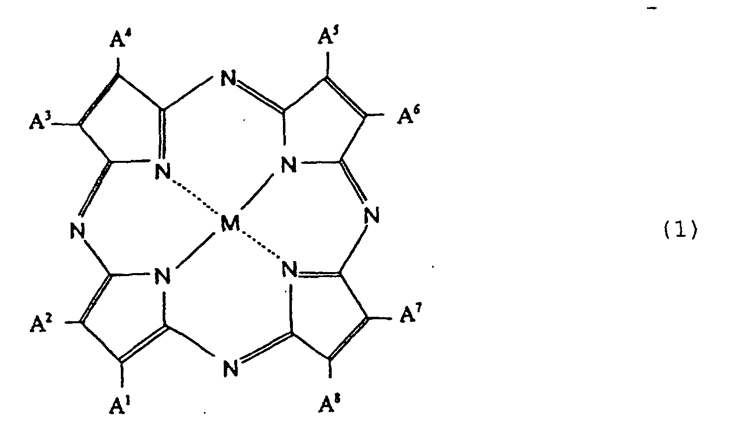
- The display filter of claim 10, wherein a near-infrared ray absorption dye having an absorption maximum in a wavelength range of from 800 to 1100 nm is contained.
- The display filter of any one of claims 1 to 6, wherein visible light ray reflectance on a surface of the functional transparent layer (A) is 2% or less.
- The display filter of any one of claims 1 to 15, wherein visible light ray transmittance is from 30 to 85%.
- The display filter of any one of claims 1 to 16, wherein transmittance minimum in a wavelength range of from 800 to 1100 nm is 20% or less.
- The display filter of any one of claims 1 to 6, wherein a total thickness of the polymer film in entirety of the filter is 0.3 mm or more.
- The display filter of any one of claims 1 to 18, wherein a polymer film for increasing a total thickness capable of containing a dye is provided.
- The display filter of claim 2 or 3, wherein an electrode electrically connected with the transparent electrically conductive layer (D) is formed.
- The display filter of claim 20, wherein the electrode electrically contacting with the transparent electrically conductive layer (D) is continuously formed along a circumferential direction in a peripheral portion of the filter.
- The display filter of claim 20, wherein an electrode is formed in an electrically conducting portion a part of which is exposed.
- The display filter of claim 21 or 22, wherein the filter is shaped into a rectangle and electrodes are formed in two surrounding sides facing to each other.
- The display filter of claim 21 or 22, where the electrode electrically connected with the transparent electrically conductive layer (D) is formed on a surface of a peripheral edge of the filter.
- The display filter of any one of claims 1 to 6, wherein a communicating hole which communicates from an outermost surface of the filter through to at least the transparent electrically conductive layer (D) is formed along a thickness direction of the filter wherein an electrode which electrically is connected with the transparent electrically conductive layer (D) is formed inside the communication hole.
- The display filter of any one of claims 1 to 6, wherein an electrically conductive tape is interposed between the transparent electrically conductive layer (D) and a layer adjacent to the transparent electrically conductive layer (D).
- A display apparatus, comprising:a display for representing an image; anda display filter of any one of claims 1 to 26, disposed on a display screen.
- A method for production of a display apparatus, comprising the steps of:laminating a display filter of any one of claims 20 to 26 on a display screen of a display apparatus via a transparent adhesive layer (C); andelectrically connecting a ground conductor of the display apparatus and the electrode of the transparent electrically conductive layer (D).
- A method of production of a display apparatus, comprising the steps of:laminating a laminate filter comprising a polymer film (B), a transparent electrically conductive layer (D), and a transparent adhesive layer (C) on a display screen via the transparent adhesive layer (C);arranging a functional transparent layer (A) having an anti-reflection property and/or an anti-glare property on the laminate filter directly or via a second adhesive layer; andelectrically connecting a ground conductor of the display apparatus and the transparent electrically conductive layer (D).
- A method for production of a display apparatus, characterized by comprising the steps of:arranging an adhesive layer on a display screen of a display apparatus;bonding a laminate filter comprising a polymer film (B), a transparent electrically conductive layer (D), and a functional transparent layer (A) having an anti-reflection property and/or an anti-glare property on the display screen via the adhesive layer; andelectrically connecting a ground conductor and the transparent electrically conductive layer (D).
- A method for production of a display apparatus, comprising the steps of:arranging an adhesive layer on a display screen;bonding a laminate filter comprising a polymer film (B), and a transparent electrically conductive layer (D) on the display screen via the adhesive layer;arranging a functional transparent layer (A) having an anti-reflection property and/or an anti-glare property on the laminate filter directly or via a second adhesive layer; andelectrically connecting a ground conductor and the transparent electrically conductive layer (D).
Applications Claiming Priority (13)
| Application Number | Priority Date | Filing Date | Title |
|---|---|---|---|
| JP2000024183 | 2000-02-01 | ||
| JP2000024185 | 2000-02-01 | ||
| JP2000024184 | 2000-02-01 | ||
| JP2000024184 | 2000-02-01 | ||
| JP2000024183 | 2000-02-01 | ||
| JP2000024185 | 2000-02-01 | ||
| JP2000180501 | 2000-06-15 | ||
| JP2000180501 | 2000-06-15 | ||
| JP2000213431 | 2000-07-13 | ||
| JP2000213431 | 2000-07-13 | ||
| JP2000384101 | 2000-12-18 | ||
| JP2000384101 | 2000-12-18 | ||
| PCT/JP2001/000695 WO2001057833A1 (en) | 2000-02-01 | 2001-02-01 | Filter for displaying, display unit and production method therefor |
Publications (2)
| Publication Number | Publication Date |
|---|---|
| EP1267318A1 true EP1267318A1 (en) | 2002-12-18 |
| EP1267318A4 EP1267318A4 (en) | 2005-12-14 |
Family
ID=27554719
Family Applications (1)
| Application Number | Title | Priority Date | Filing Date |
|---|---|---|---|
| EP01949054A Withdrawn EP1267318A4 (en) | 2000-02-01 | 2001-02-01 | Filter for displaying, display unit and production method therefor |
Country Status (5)
| Country | Link |
|---|---|
| US (1) | US6965191B2 (en) |
| EP (1) | EP1267318A4 (en) |
| KR (1) | KR100590368B1 (en) |
| CN (1) | CN1234107C (en) |
| WO (1) | WO2001057833A1 (en) |
Cited By (17)
| Publication number | Priority date | Publication date | Assignee | Title |
|---|---|---|---|---|
| WO2001010971A1 (en) | 1999-08-04 | 2001-02-15 | Skc Co., Ltd. | Selectively light-absorptive material, coating composition containing the same, and filter manufactured using the coating composition for color displays |
| WO2004066342A1 (en) * | 2003-01-23 | 2004-08-05 | Skc Limited | Plasma display panel filter |
| EP1530065A1 (en) * | 2003-11-06 | 2005-05-11 | Rohm and Haas Electronic Materials, L.L.C. | Optical article |
| EP1643277A1 (en) * | 2004-09-29 | 2006-04-05 | Fujitsu Hitachi Plasma Display Limited | Display filter |
| EP1691392A2 (en) | 2004-12-23 | 2006-08-16 | Lg Electronics Inc. | Plasma display panel apparatus |
| EP1717608A1 (en) * | 2005-04-29 | 2006-11-02 | LG Electronics Inc. | Filter for display apparatus and plasma display apparatus comprising filter |
| EP1755139A1 (en) * | 2005-07-21 | 2007-02-21 | LG Electronics Inc. | Plasma display apparatus |
| EP1775605A1 (en) * | 2005-10-11 | 2007-04-18 | LG Electronics Inc. | Display filter and plasma display apparatus |
| EP1816495A1 (en) * | 2006-02-01 | 2007-08-08 | Samsung SDI Co., Ltd. | Optical filter and plasma display panel employing the same |
| EP1895563A3 (en) * | 2006-08-31 | 2008-12-17 | Hitachi Plasma Display Limited | Display panel module and manufactruring method therefor |
| EP1889278A4 (en) * | 2005-06-09 | 2009-04-15 | Lg Chemical Ltd | A pdp filter and manufacturing method thereof using a fully etched electromagnetic interference film |
| EP1835522A3 (en) * | 2006-03-13 | 2009-06-03 | LG Electronics Inc. | Plasma display apparatus and method of manufacturing the same |
| EP1692710A4 (en) * | 2003-12-10 | 2009-07-15 | Lg Chemical Ltd | METHOD FOR MANUFACTURING ASSY FILM USED IN PDP FILTER, ASSY FILM MANUFACTURED THEREBY, AND FILM PDP FILTER ASSY |
| EP1856711A4 (en) * | 2005-03-04 | 2009-10-28 | Lg Chemical Ltd | Pdp filter and manufacturing method thereof |
| EP2048929A4 (en) * | 2006-02-08 | 2010-08-25 | Bridgestone Corp | Method for manufacturing optical filter for display, optical filter for display, and display and plasma display panel provided with such optical filter |
| US7973875B2 (en) | 2005-08-24 | 2011-07-05 | Toray Advanced Film Co., Ltd | Flat-panel display member and its manufacturing method and flat-panel display and its manufacturing method |
| EP3321718A4 (en) * | 2015-07-10 | 2019-01-16 | Dexerials Corporation | PHOPHORE SHEET, WHITE LIGHT SOURCE DEVICE HAVING SAME PHOSPHORO SHEET, AND DISPLAY APPARATUS HAVING SAID WHITE LIGHT SOURCE DEVICE |
Families Citing this family (137)
| Publication number | Priority date | Publication date | Assignee | Title |
|---|---|---|---|---|
| CA2353506A1 (en) | 1998-11-02 | 2000-05-11 | 3M Innovative Properties Company | Transparent conductive oxides for plastic flat panel displays |
| KR100939747B1 (en) * | 2001-05-16 | 2010-02-04 | 가부시키가이샤 브리지스톤 | Electromagnetic shielding light transmitting window material, manufacturing method thereof and display panel |
| WO2003032332A1 (en) * | 2001-10-05 | 2003-04-17 | Bridgestone Corporation | Transparent electroconductive film, method for manufacture thereof, and touch panel |
| JP2003255343A (en) * | 2002-03-05 | 2003-09-10 | Citizen Electronics Co Ltd | Front light for color liquid crystal display |
| TW200428268A (en) * | 2002-07-15 | 2004-12-16 | Fuji Photo Film Co Ltd | Internal touch panel, and process for producing it and display device |
| FR2843204B1 (en) * | 2002-08-05 | 2004-09-17 | Saint Gobain | OPTICAL FILTERING AND ELECTROMAGNETIC SHIELDING STRUCTURE |
| JP4360788B2 (en) * | 2002-08-29 | 2009-11-11 | シチズン電子株式会社 | Backlight for liquid crystal display panel and method of manufacturing light emitting diode used therefor |
| JP2004127719A (en) * | 2002-10-02 | 2004-04-22 | Nippon Hoso Kyokai <Nhk> | Transparent conductive film and display device |
| KR100499062B1 (en) * | 2002-11-01 | 2005-07-01 | 엘지전자 주식회사 | Plasma display panel |
| JP4181862B2 (en) * | 2002-11-28 | 2008-11-19 | 篠田プラズマ株式会社 | Arc tube array type display device |
| JP2004206076A (en) * | 2002-12-10 | 2004-07-22 | Pioneer Electronic Corp | Flat display device |
| JP2004241130A (en) * | 2003-02-03 | 2004-08-26 | Seiko Epson Corp | Light emitting display panel and manufacturing method thereof |
| KR100911034B1 (en) * | 2003-03-12 | 2009-08-06 | 엘지전자 주식회사 | Front filter of plasma display panel |
| US7883421B2 (en) * | 2003-03-17 | 2011-02-08 | Igt | Gaming apparatus having a display with a conductive coating |
| KR100515573B1 (en) * | 2003-03-20 | 2005-09-20 | 주식회사 엘지화학 | Electro-magnetic shielding filter for plasma display panel and method for preparating the same |
| KR20040085699A (en) * | 2003-04-01 | 2004-10-08 | 엘지전자 주식회사 | Front filter of plasma display panel |
| TW584356U (en) * | 2003-04-25 | 2004-04-11 | Optimax Tech Corp | Display panel structure |
| JP3812550B2 (en) * | 2003-07-07 | 2006-08-23 | セイコーエプソン株式会社 | Tunable optical filter |
| KR100630321B1 (en) * | 2003-07-18 | 2006-09-29 | 미쓰이 가가쿠 가부시키가이샤 | Laminate and uses thereof |
| EP1511095A3 (en) * | 2003-08-19 | 2011-02-23 | LG Display Co., Ltd. | Organic electroluminescent device and method of manufacturing the same |
| US7414204B2 (en) * | 2003-10-29 | 2008-08-19 | Samsung Sdi Co., Ltd. | Display device and heat dissipating means therefor |
| JP4243237B2 (en) * | 2003-11-10 | 2009-03-25 | 淳二 城戸 | Organic element, organic EL element, organic solar cell, organic FET structure, and organic element manufacturing method |
| US20050163958A1 (en) * | 2003-11-13 | 2005-07-28 | Yuji Nakatsugawa | Optical filter and display using the same |
| KR100515575B1 (en) * | 2003-12-10 | 2005-09-20 | 주식회사 엘지화학 | Optical filter for plasma display panel and manufacturing method thereof |
| WO2005081210A1 (en) * | 2004-02-20 | 2005-09-01 | Nissha Printing Co., Ltd. | Protection panel for electronic apparatus display window and production method for protection panel |
| WO2005080453A1 (en) * | 2004-02-23 | 2005-09-01 | Lg Chem, Ltd. | Adhesive film functionalizing color compensation and near infrared ray (nir) blocking and plasma display panel filter using the same |
| US20070264499A1 (en) * | 2004-02-23 | 2007-11-15 | Lg Chem, Ltd. | Adhesive film functionalizing color compensation and near infrared ray (NIR) blocking and plasma display panel filter using the same |
| WO2005088587A1 (en) * | 2004-03-10 | 2005-09-22 | Sumitomo Osaka Cement Co., Ltd. | Transparent laminate |
| US7851035B2 (en) * | 2004-04-26 | 2010-12-14 | Koa Glass Co., Ltd. | Multicolor glass vessel |
| JP4541108B2 (en) * | 2004-04-26 | 2010-09-08 | パナソニック株式会社 | Plasma display device |
| JP4636857B2 (en) * | 2004-05-06 | 2011-02-23 | パナソニック株式会社 | Plasma display device |
| KR20060000775A (en) * | 2004-06-29 | 2006-01-06 | 삼성에스디아이 주식회사 | Optical Filter for Dual Image Reduction and Plasma Display Panel |
| KR100669721B1 (en) * | 2004-08-18 | 2007-01-16 | 삼성에스디아이 주식회사 | Electromagnetic shielding film for improving color and plasma display device |
| CN100365444C (en) * | 2004-08-31 | 2008-01-30 | 精碟科技股份有限公司 | Optical filter manufacturing method |
| US7569277B2 (en) * | 2004-09-30 | 2009-08-04 | Dai Nippon Printing Co., Ltd. | Optical laminate |
| TWI237409B (en) * | 2004-10-08 | 2005-08-01 | Kingbright Electronics Co Ltd | Method of fabricating light emitting diode (LED) |
| US7099067B2 (en) * | 2004-11-10 | 2006-08-29 | Photon Dynamics, Inc. | Scratch and mar resistant PDLC modulator |
| KR100592313B1 (en) * | 2004-11-22 | 2006-06-21 | 삼성에스디아이 주식회사 | Plasma display panel |
| US20060121392A1 (en) * | 2004-11-24 | 2006-06-08 | Dai Nippon Printing Co., Ltd. | Optical filter and display using the same |
| EP1666927A1 (en) * | 2004-12-03 | 2006-06-07 | Nanogate Advanced Materials GmbH | Solar protection sheet |
| KR100761646B1 (en) * | 2004-12-28 | 2007-09-27 | 토요 보세키 가부시기가이샤 | Wavelength-selective absorption filter |
| TWI266902B (en) * | 2005-01-19 | 2006-11-21 | Lg Chemical Ltd | Filter for plasma display panel with good re-workability and plasma display panel comprising the same |
| KR20060084246A (en) * | 2005-01-19 | 2006-07-24 | 삼성에스디아이 주식회사 | Plasma display device |
| EP1847580B1 (en) * | 2005-01-21 | 2009-08-26 | Asahi Glass Company, Limited | Pressure-sensitive adhesive composition and optical filter |
| JP4660217B2 (en) * | 2005-01-31 | 2011-03-30 | 株式会社東芝 | Storage medium, reproducing method, recording method, reproducing apparatus and recording apparatus |
| JP4600660B2 (en) * | 2005-02-07 | 2010-12-15 | 住友金属鉱山株式会社 | Faraday rotator for high power laser |
| JP2006244745A (en) * | 2005-03-01 | 2006-09-14 | Hitachi Ltd | Display panel |
| JP4417869B2 (en) * | 2005-03-15 | 2010-02-17 | 株式会社東芝 | Information storage medium, reproducing method and recording method |
| US20060231189A1 (en) * | 2005-04-15 | 2006-10-19 | Solutia, Inc. | Low moisture polymer sheets |
| KR100761160B1 (en) * | 2005-04-19 | 2007-09-21 | 엘지전자 주식회사 | Filter for plasma display device and manufacturing method thereof, plasma display device comprising same |
| US20060286465A1 (en) * | 2005-06-15 | 2006-12-21 | Ji-Suk Kim | Film type filter and display apparatus comprising the same |
| JP4867055B2 (en) * | 2005-06-30 | 2012-02-01 | 富士フイルム株式会社 | Dispersive electroluminescence device |
| US20070108897A1 (en) * | 2005-11-15 | 2007-05-17 | Jonnalagadda Krishna D | Electroluminescent display having electric shock prevention |
| US20070139576A1 (en) * | 2005-12-21 | 2007-06-21 | Alexander Hunt | Display module for an electronic device |
| JP4462197B2 (en) | 2006-01-23 | 2010-05-12 | ソニー株式会社 | Optical low-pass filter |
| KR20070099830A (en) * | 2006-04-05 | 2007-10-10 | 삼성코닝 주식회사 | Optical Filters for Display Devices |
| JP4948022B2 (en) * | 2006-04-13 | 2012-06-06 | 株式会社Adeka | Optical filter |
| US7508586B2 (en) * | 2006-04-14 | 2009-03-24 | Southwall Technologies, Inc. | Zinc-based film manipulation for an optical filter |
| KR20070106328A (en) * | 2006-04-28 | 2007-11-01 | 엘지전자 주식회사 | Filter for display device and plasma display device including same |
| WO2007148411A1 (en) * | 2006-06-22 | 2007-12-27 | Pioneer Corporation | Display device |
| KR100962924B1 (en) * | 2006-07-14 | 2010-06-10 | 삼성코닝정밀소재 주식회사 | Electromagnetic shielding optical member, optical filter and display device comprising same |
| WO2008011547A1 (en) * | 2006-07-20 | 2008-01-24 | Cpfilms Inc. | Composite, color corrected films comprising an aluminum oxide coating |
| US20080020232A1 (en) * | 2006-07-20 | 2008-01-24 | Lisa Yvonne Winckler | Solar Control Polymer Films Comprising an Aluminum Oxide Coating |
| US8441467B2 (en) * | 2006-08-03 | 2013-05-14 | Perceptive Pixel Inc. | Multi-touch sensing display through frustrated total internal reflection |
| CN100462749C (en) * | 2006-08-31 | 2009-02-18 | 甘国工 | Filter plate having electromagnetic radiation prevention and light filtering function of plasma display |
| JP5022666B2 (en) * | 2006-10-23 | 2012-09-12 | 株式会社日立製作所 | Plasma display device |
| KR100837160B1 (en) * | 2006-10-25 | 2008-06-11 | 엘지전자 주식회사 | Plasma display device |
| KR20080055332A (en) * | 2006-12-15 | 2008-06-19 | 엘지전자 주식회사 | Composition of electromagnetic wave shielding paste, display filter and plasma display panel using same |
| WO2008081837A1 (en) * | 2006-12-27 | 2008-07-10 | Asahi Glass Company, Limited | Anti-reflection product and display device |
| KR101511799B1 (en) | 2006-12-28 | 2015-04-13 | 쓰리엠 이노베이티브 프로퍼티즈 컴파니 | Nucleation layer for thin film metal layer formation |
| KR100775847B1 (en) * | 2007-01-25 | 2007-11-13 | 엘지전자 주식회사 | Plasma Display Panel |
| KR100911008B1 (en) * | 2007-05-31 | 2009-08-05 | 삼성에스디아이 주식회사 | Film filter and plasma display device having same |
| US8623498B2 (en) * | 2007-10-26 | 2014-01-07 | Teijin Limited | Transparent electroconductive laminate and transparent touch panel |
| EP2212726A1 (en) * | 2007-10-30 | 2010-08-04 | 3M Innovative Properties Company | Multi-stack optical bandpass film with electro magnetic interference shielding for optical display filters |
| WO2009075348A1 (en) * | 2007-12-12 | 2009-06-18 | Bridgestone Corporation | Optical filter, optical filter for display, display provided with such filter, and plasma display panel |
| KR100975200B1 (en) * | 2008-02-29 | 2010-08-10 | 삼성에스디아이 주식회사 | Single sheet type film filter and manufacturing method thereof and plasma display device using same |
| US7824777B2 (en) * | 2008-03-26 | 2010-11-02 | Southwall Technologies, Inc. | Robust optical filter utilizing pairs of dielectric and metallic layers |
| KR100989129B1 (en) * | 2008-04-03 | 2010-10-20 | 삼성모바일디스플레이주식회사 | Display device |
| US8329304B2 (en) * | 2008-05-27 | 2012-12-11 | Guardian Industries Corp. | Plasma display panel including TCC EMI filter, and/or method of making the same |
| US8350451B2 (en) | 2008-06-05 | 2013-01-08 | 3M Innovative Properties Company | Ultrathin transparent EMI shielding film comprising a polymer basecoat and crosslinked polymer transparent dielectric layer |
| DE102009026834A1 (en) * | 2008-06-11 | 2009-12-24 | Samsung Corning Precision Glass Co., Ltd., Gumi | Filter and display device with the same |
| US20090309838A1 (en) * | 2008-06-11 | 2009-12-17 | Microsoft Corporation | Use of separation elements with rear projection screen |
| EP2302422A4 (en) * | 2008-07-17 | 2013-01-09 | Toray Advanced Film Co Ltd | FILTER FOR DISPLAY DEVICE |
| KR20100024132A (en) * | 2008-08-25 | 2010-03-05 | 엘지전자 주식회사 | Plasma displasy device and glass filter for the same |
| CN101928489B (en) * | 2008-12-19 | 2012-07-11 | 京东方科技集团股份有限公司 | Pigment dispersion, pigment photoresist and color filter |
| KR101298356B1 (en) * | 2008-12-19 | 2013-08-20 | 엘지디스플레이 주식회사 | Liquid Crystal Display Device |
| CA2751559A1 (en) * | 2009-02-05 | 2010-08-12 | Koninklijke Philips Electronics N.V. | Electroluminescent device |
| US8314986B2 (en) * | 2009-03-25 | 2012-11-20 | Fujifilm Corporation | Transparent electromagnetic wave-shielding filter and method of producing thereof, and conductive film |
| WO2010109380A2 (en) * | 2009-03-27 | 2010-09-30 | Koninklijke Philips Electronics N.V. | A device for placement in front of a display device |
| AU2010236468A1 (en) * | 2009-04-15 | 2011-10-13 | Research Triangle Institute | Stimulated lighting devices |
| US20120112618A1 (en) * | 2009-07-29 | 2012-05-10 | Sharp Kabushiki Kaisha | Organic electroluminescence illuminating device and method for manufacturing the same |
| CN102474999B (en) | 2009-08-03 | 2016-09-07 | 3M创新有限公司 | For the method forming optically transparent conducting metal or emtal alloy film and the film being made from |
| US20110033668A1 (en) * | 2009-08-07 | 2011-02-10 | Boelstler Richard A | Apparatus and method for illuminating through a circuit board |
| JP2011113061A (en) * | 2009-11-30 | 2011-06-09 | Brother Industries Ltd | Antiglare film and display device |
| KR101702127B1 (en) * | 2010-03-25 | 2017-02-02 | 엘지전자 주식회사 | Display apparatus |
| US9932267B2 (en) | 2010-03-29 | 2018-04-03 | Vitro, S.A.B. De C.V. | Solar control coatings with discontinuous metal layer |
| US10654747B2 (en) | 2010-03-29 | 2020-05-19 | Vitro Flat Glass Llc | Solar control coatings with subcritical copper |
| US10654748B2 (en) | 2010-03-29 | 2020-05-19 | Vitro Flat Glass Llc | Solar control coatings providing increased absorption or tint |
| CN101847554B (en) * | 2010-06-01 | 2011-12-07 | 四川长虹电器股份有限公司 | Light filter electromagnetic shielding membrane extraction electrode manufacturing method |
| JP5785798B2 (en) * | 2010-06-30 | 2015-09-30 | 富士フイルム株式会社 | Method for producing antistatic laminate |
| US8824006B2 (en) * | 2010-08-23 | 2014-09-02 | Kabushiki Kaisha Toshiba | Color correction apparatus and color correction method |
| KR101340549B1 (en) * | 2010-12-30 | 2013-12-11 | 제일모직주식회사 | Optical film and display filter comprising the same |
| JP2012189683A (en) * | 2011-03-09 | 2012-10-04 | Nitto Denko Corp | Infrared ray reflection film |
| US8749529B2 (en) * | 2012-03-01 | 2014-06-10 | Microsoft Corporation | Sensor-in-pixel display system with near infrared filter |
| JP2013196531A (en) * | 2012-03-22 | 2013-09-30 | Japan Display Inc | Touch panel and display device with touch panel |
| KR102155239B1 (en) * | 2012-05-29 | 2020-09-11 | 스미또모 가가꾸 가부시키가이샤 | Colored curable resin composition |
| CN102749307A (en) * | 2012-07-27 | 2012-10-24 | 哈尔滨工业大学 | Measuring method of optical constant of semi-transparent solid material |
| KR102120423B1 (en) * | 2013-09-16 | 2020-06-09 | 삼성디스플레이 주식회사 | Display device and method of manufacturing the same |
| US9498382B2 (en) * | 2013-10-29 | 2016-11-22 | Oberon Company Div Paramount Corp. | Grey compounded infrared absorbing faceshield |
| JP2015122148A (en) * | 2013-12-20 | 2015-07-02 | 株式会社ジャパンディスプレイ | Organic electroluminescence display device |
| KR20150102553A (en) * | 2014-02-28 | 2015-09-07 | (주)엘지하우시스 | Interior film having excellent metallic appearance and method of manufacturing the same |
| KR20160024003A (en) * | 2014-08-21 | 2016-03-04 | 삼성에스디아이 주식회사 | Window film and display apparatus comprising the same |
| JP6507523B2 (en) * | 2014-08-22 | 2019-05-08 | コニカミノルタ株式会社 | Organic electroluminescent device |
| KR102224029B1 (en) * | 2014-08-22 | 2021-03-09 | 엘지디스플레이 주식회사 | Organic light emitting display panel and display device |
| TWI675907B (en) | 2015-01-21 | 2019-11-01 | 日商Jsr股份有限公司 | Solid imaging device |
| MX2017009426A (en) * | 2015-03-09 | 2017-10-12 | Vision Ease Lp | Anti-static, anti-reflective coating. |
| WO2017087604A1 (en) * | 2015-11-18 | 2017-05-26 | Everix, Inc. | Interference filter film for display applications |
| CN105703839B (en) * | 2016-01-08 | 2018-01-12 | 清华大学 | A kind of visible light communication system |
| KR102769963B1 (en) * | 2016-10-31 | 2025-02-17 | 엘지디스플레이 주식회사 | Liquid crystal display device |
| CN107066920A (en) * | 2016-12-23 | 2017-08-18 | 浙江大学 | Fingerprint recognition panel and device |
| MX2019004737A (en) | 2017-01-03 | 2019-06-17 | Corning Inc | Vehicle interior systems having a curved cover glass and a display or touch panel and methods for forming the same. |
| WO2019004042A1 (en) * | 2017-06-27 | 2019-01-03 | 住友化学株式会社 | Optical film |
| CN111094050B (en) | 2017-07-18 | 2023-11-07 | 康宁公司 | Cold forming of complex curved glass products |
| CN107219723B (en) * | 2017-08-02 | 2021-01-22 | 京东方科技集团股份有限公司 | Manufacturing method of metal grating, metal grating and display device |
| WO2019055469A1 (en) | 2017-09-12 | 2019-03-21 | Corning Incorporated | Deadfront for displays including a touch panel on decorative glass and related methods |
| US11065960B2 (en) | 2017-09-13 | 2021-07-20 | Corning Incorporated | Curved vehicle displays |
| CN107526127A (en) * | 2017-09-18 | 2017-12-29 | 江门市卡色光学有限公司 | One kind strengthens tempering filter |
| TWI844520B (en) | 2017-10-10 | 2024-06-11 | 美商康寧公司 | Vehicle interior systems having a curved cover glass with improved reliability and methods for forming the same |
| US11078718B2 (en) | 2018-02-05 | 2021-08-03 | Vitro Flat Glass Llc | Solar control coatings with quadruple metallic layers |
| WO2019182051A1 (en) | 2018-03-20 | 2019-09-26 | 凸版印刷株式会社 | Optical element and authentication body |
| US10562812B2 (en) | 2018-06-12 | 2020-02-18 | Guardian Glass, LLC | Coated article having metamaterial-inclusive layer, coating having metamaterial-inclusive layer, and/or method of making the same |
| US10830933B2 (en) | 2018-06-12 | 2020-11-10 | Guardian Glass, LLC | Matrix-embedded metamaterial coating, coated article having matrix-embedded metamaterial coating, and/or method of making the same |
| JP2021531494A (en) * | 2018-07-12 | 2021-11-18 | コーニング インコーポレイテッド | Dead front made for color matching |
| CN111273459B (en) * | 2020-03-16 | 2025-01-24 | 中国人民解放军63919部队 | A microwave protection transparent dielectric material and its preparation method and application |
| CN111443834A (en) * | 2020-04-28 | 2020-07-24 | 北京载诚科技有限公司 | Conductive film structure |
| CN113763808A (en) * | 2020-06-05 | 2021-12-07 | 华为技术有限公司 | Flexible display cover plate, preparation method thereof and flexible display module |
| KR102471503B1 (en) | 2021-10-26 | 2022-11-28 | 회명산업 주식회사 | Black paste composition for coating protection film of plasmadisplay panel and cured product thereof |
Family Cites Families (45)
| Publication number | Priority date | Publication date | Assignee | Title |
|---|---|---|---|---|
| JPS58153904A (en) | 1982-03-08 | 1983-09-13 | Mitsubishi Rayon Co Ltd | Plastic filter |
| JPS59221943A (en) | 1983-05-31 | 1984-12-13 | Kyowa Gas Chem Ind Co Ltd | Color display with distinct coloring |
| JPS6022102A (en) | 1983-07-18 | 1985-02-04 | Mitsubishi Rayon Co Ltd | Optical filter system |
| US4841372A (en) * | 1986-08-08 | 1989-06-20 | Zenith Electronics Corporation | Cathode ray tube contrast enhancement systems |
| US5271872A (en) * | 1988-11-25 | 1993-12-21 | Gentex Corporation | Laser-attenuative optical filter |
| EP0596531B1 (en) | 1992-11-06 | 1997-07-09 | Kabushiki Kaisha Toshiba | Antireflection film and display apparatus comprising the same |
| US5506079A (en) | 1994-02-28 | 1996-04-09 | Ricoh Company, Ltd. | Magnetic composition, magnetic toner and ink containing the magnetic composition |
| JPH0837105A (en) | 1994-02-28 | 1996-02-06 | Gligorian Leonide | Magnetic composition, magnetic toner and magnetic ink |
| US5879217A (en) * | 1995-02-14 | 1999-03-09 | Sony Corporation | Cathode ray tube and method of manufacturing the same |
| JPH08220303A (en) | 1995-02-17 | 1996-08-30 | Kyodo Printing Co Ltd | Optical member for display and supporting method thereof |
| JPH0951494A (en) | 1995-08-07 | 1997-02-18 | Fujitsu General Ltd | Plasma display device with optical filter |
| US5804102A (en) * | 1995-12-22 | 1998-09-08 | Mitsui Chemicals, Inc. | Plasma display filter |
| JPH09230797A (en) | 1996-02-20 | 1997-09-05 | Sony Corp | Display device and method of manufacturing the same |
| JP3618448B2 (en) | 1996-03-13 | 2005-02-09 | 株式会社富士通ゼネラル | Electromagnetic wave leakage prevention filter |
| TW446637B (en) * | 1996-05-28 | 2001-07-21 | Mitsui Chemicals Inc | Transparent laminates and optical filters for displays using the same |
| JP3473310B2 (en) * | 1996-07-01 | 2003-12-02 | 日立化成工業株式会社 | Display film having electromagnetic wave shielding property and infrared ray shielding property, electromagnetic wave shielding body, and method of manufacturing plasma display |
| JP3841484B2 (en) | 1996-07-25 | 2006-11-01 | オリンパス株式会社 | Microscope epi-illumination system |
| JP3753482B2 (en) | 1996-10-22 | 2006-03-08 | 三井化学株式会社 | Transparent laminate and display filter using the same |
| JP4148548B2 (en) | 1996-11-07 | 2008-09-10 | 富士フイルム株式会社 | Antireflection film and plasma display using the same |
| US5945209A (en) | 1996-11-07 | 1999-08-31 | Fuji Photo Film Co., Ltd. | Anti-reflection film and plasma display panel |
| JPH10156991A (en) | 1996-11-28 | 1998-06-16 | Asahi Chem Ind Co Ltd | Antireflective film with near infrared ray absorbing characteristics |
| JPH10187056A (en) | 1996-12-19 | 1998-07-14 | Sony Corp | Filter for display device, display device, and front panel for display device |
| JP4163268B2 (en) | 1996-12-25 | 2008-10-08 | 日東電工株式会社 | Plasma display panel filter and plasma display device using the same |
| JPH10211668A (en) | 1997-01-31 | 1998-08-11 | Toyobo Co Ltd | Infrared ray absorption film |
| JPH11130971A (en) | 1997-07-23 | 1999-05-18 | Ricoh Co Ltd | Tetraazaporphyrin compound and precursor thereof and method for producing tetraazaporphyrin compound |
| JPH1165463A (en) | 1997-08-13 | 1999-03-05 | Asahi Chem Ind Co Ltd | Display front panel having also wavelength selectivity |
| US6255778B1 (en) | 1997-10-13 | 2001-07-03 | Bridgestone Corporation | Plasma display panel having electromagnetic wave shielding material attached to front surface of display |
| JP4111571B2 (en) | 1997-10-13 | 2008-07-02 | 株式会社ブリヂストン | Display panel |
| JPH11126024A (en) | 1997-10-22 | 1999-05-11 | Dainippon Printing Co Ltd | Front panel for display |
| JPH11185641A (en) | 1997-12-22 | 1999-07-09 | Bridgestone Corp | Display panel |
| JP3997581B2 (en) | 1998-01-13 | 2007-10-24 | 株式会社ブリヂストン | Display panel |
| JPH11281816A (en) | 1998-01-28 | 1999-10-15 | Minnesota Mining & Mfg Co <3M> | Optical filter |
| JPH11212475A (en) | 1998-01-28 | 1999-08-06 | Bridgestone Corp | Display panel |
| JP3480898B2 (en) | 1998-02-12 | 2003-12-22 | 日立化成工業株式会社 | Electromagnetic wave shielding film for display, electromagnetic wave shielding structure for display and display |
| JPH11251782A (en) | 1998-03-06 | 1999-09-17 | Bridgestone Corp | Light-transmissive electromagnetic-wave shielding window member |
| JPH11282365A (en) | 1998-03-31 | 1999-10-15 | Mitsui Chem Inc | Electromagnetic wave shield for plasma display |
| JPH11344935A (en) | 1998-05-29 | 1999-12-14 | Oike Ind Co Ltd | Film laminate for affixation to display front surface plate and display front surface plate |
| JP2000059085A (en) | 1998-06-04 | 2000-02-25 | Nippon Carbide Ind Co Inc | Electromagnetic wave shield film |
| JP3898357B2 (en) | 1998-09-28 | 2007-03-28 | 日東電工株式会社 | Filter for plasma display panel |
| JP2000216589A (en) | 1999-01-25 | 2000-08-04 | Nippon Carbide Ind Co Inc | Electromagnetic shield structure of display panel |
| JP2000258626A (en) | 1999-03-09 | 2000-09-22 | Mitsubishi Chemicals Corp | Plasma display filter |
| JP3849070B2 (en) | 1999-06-30 | 2006-11-22 | 株式会社日立プラズマパテントライセンシング | Flat panel display |
| EP1071147A1 (en) | 1999-07-19 | 2001-01-24 | Toshiba Battery Co., Ltd. | Battery pack |
| US6678016B1 (en) * | 1999-12-30 | 2004-01-13 | Sony Corporation | Filter for display device and display device |
| US6797396B1 (en) * | 2000-06-09 | 2004-09-28 | 3M Innovative Properties Company | Wrinkle resistant infrared reflecting film and non-planar laminate articles made therefrom |
-
2001
- 2001-02-01 KR KR1020027009915A patent/KR100590368B1/en not_active Expired - Fee Related
- 2001-02-01 EP EP01949054A patent/EP1267318A4/en not_active Withdrawn
- 2001-02-01 WO PCT/JP2001/000695 patent/WO2001057833A1/en not_active Ceased
- 2001-02-01 US US10/182,774 patent/US6965191B2/en not_active Expired - Fee Related
- 2001-02-01 CN CNB018044190A patent/CN1234107C/en not_active Expired - Fee Related
Cited By (28)
| Publication number | Priority date | Publication date | Assignee | Title |
|---|---|---|---|---|
| WO2001010971A1 (en) | 1999-08-04 | 2001-02-15 | Skc Co., Ltd. | Selectively light-absorptive material, coating composition containing the same, and filter manufactured using the coating composition for color displays |
| WO2004066342A1 (en) * | 2003-01-23 | 2004-08-05 | Skc Limited | Plasma display panel filter |
| CN100527311C (en) * | 2003-01-23 | 2009-08-12 | 爱思开哈斯显示器薄膜有限公司 | Plasma display panel filter |
| EP1530065A1 (en) * | 2003-11-06 | 2005-05-11 | Rohm and Haas Electronic Materials, L.L.C. | Optical article |
| US8716824B2 (en) | 2003-11-06 | 2014-05-06 | Rohm And Haas Electronic Materials Llc | Article having electrically conductive and selectively passivated patterns |
| US8198120B2 (en) | 2003-11-06 | 2012-06-12 | Rohm And Haas Electronic Materials Llc | Optical article |
| EP1692710A4 (en) * | 2003-12-10 | 2009-07-15 | Lg Chemical Ltd | METHOD FOR MANUFACTURING ASSY FILM USED IN PDP FILTER, ASSY FILM MANUFACTURED THEREBY, AND FILM PDP FILTER ASSY |
| US7709751B2 (en) | 2003-12-10 | 2010-05-04 | Lg Chem, Ltd. | Method for making film assembly used in PDP filter, film assembly manufactured by the method, and PDP filter with the film assembly |
| EP1643277A1 (en) * | 2004-09-29 | 2006-04-05 | Fujitsu Hitachi Plasma Display Limited | Display filter |
| EP1691392A2 (en) | 2004-12-23 | 2006-08-16 | Lg Electronics Inc. | Plasma display panel apparatus |
| EP1691392A3 (en) * | 2004-12-23 | 2007-05-09 | Lg Electronics Inc. | Plasma display panel apparatus |
| US7567025B2 (en) | 2004-12-23 | 2009-07-28 | Lg Electronics Inc. | Plasma display panel apparatus with a film filter on panel |
| EP2242086A3 (en) * | 2005-03-04 | 2011-07-06 | LG Chem, Ltd. | PDP filter and manufacturing method thereof |
| US8004763B2 (en) | 2005-03-04 | 2011-08-23 | Lg Chem, Ltd. | PDP filter and manufacturing method thereof |
| EP1856711A4 (en) * | 2005-03-04 | 2009-10-28 | Lg Chemical Ltd | Pdp filter and manufacturing method thereof |
| EP1717608A1 (en) * | 2005-04-29 | 2006-11-02 | LG Electronics Inc. | Filter for display apparatus and plasma display apparatus comprising filter |
| EP1889278A4 (en) * | 2005-06-09 | 2009-04-15 | Lg Chemical Ltd | A pdp filter and manufacturing method thereof using a fully etched electromagnetic interference film |
| EP1755139A1 (en) * | 2005-07-21 | 2007-02-21 | LG Electronics Inc. | Plasma display apparatus |
| US7791277B2 (en) | 2005-07-21 | 2010-09-07 | Lg Electronics Inc. | Plasma display panel provided with grounding units for the assembly of the display panel and an electromagnetic interference shielding flim |
| US7973875B2 (en) | 2005-08-24 | 2011-07-05 | Toray Advanced Film Co., Ltd | Flat-panel display member and its manufacturing method and flat-panel display and its manufacturing method |
| EP1775605A1 (en) * | 2005-10-11 | 2007-04-18 | LG Electronics Inc. | Display filter and plasma display apparatus |
| EP1816495A1 (en) * | 2006-02-01 | 2007-08-08 | Samsung SDI Co., Ltd. | Optical filter and plasma display panel employing the same |
| EP2048929A4 (en) * | 2006-02-08 | 2010-08-25 | Bridgestone Corp | Method for manufacturing optical filter for display, optical filter for display, and display and plasma display panel provided with such optical filter |
| EP1835522A3 (en) * | 2006-03-13 | 2009-06-03 | LG Electronics Inc. | Plasma display apparatus and method of manufacturing the same |
| EP1895563A3 (en) * | 2006-08-31 | 2008-12-17 | Hitachi Plasma Display Limited | Display panel module and manufactruring method therefor |
| EP3321718A4 (en) * | 2015-07-10 | 2019-01-16 | Dexerials Corporation | PHOPHORE SHEET, WHITE LIGHT SOURCE DEVICE HAVING SAME PHOSPHORO SHEET, AND DISPLAY APPARATUS HAVING SAID WHITE LIGHT SOURCE DEVICE |
| US10529899B2 (en) | 2015-07-10 | 2020-01-07 | Dexerials Corporation | Phosphor sheet, white light source device including the phosphor sheet, and display device including the white light source device |
| US11183617B2 (en) | 2015-07-10 | 2021-11-23 | Dexerials Corporation | Phosphor sheet, white light source device including the phosphor sheet, and display device including the white light source device |
Also Published As
| Publication number | Publication date |
|---|---|
| CN1234107C (en) | 2005-12-28 |
| US20030156080A1 (en) | 2003-08-21 |
| WO2001057833A1 (en) | 2001-08-09 |
| KR20020077410A (en) | 2002-10-11 |
| EP1267318A4 (en) | 2005-12-14 |
| US6965191B2 (en) | 2005-11-15 |
| KR100590368B1 (en) | 2006-06-15 |
| CN1397057A (en) | 2003-02-12 |
Similar Documents
| Publication | Publication Date | Title |
|---|---|---|
| US6965191B2 (en) | Display filter, display apparatus, and method for production of the same | |
| JP3834479B2 (en) | Filter for plasma display, display device and manufacturing method thereof | |
| JP3311720B2 (en) | Display filter | |
| KR100215589B1 (en) | Transparent laminate and filter for display using the same | |
| US7163739B2 (en) | Laminate and display apparatus using the same | |
| JP3004222B2 (en) | Transparent laminate and display filter using the same | |
| JP5015644B2 (en) | Porphyrin compounds and display filters | |
| JP2006058896A (en) | Filter for plasma display, and display device and method for manufacturing the same | |
| JP3004271B2 (en) | Display filters | |
| JP3311697B2 (en) | Optical filter | |
| JP3753482B2 (en) | Transparent laminate and display filter using the same | |
| JP2002313140A (en) | Transparent conductive film, optical filter and its manufacturing method | |
| JP4004161B2 (en) | Transparent laminate and display filter using the same | |
| WO2008056947A1 (en) | Optical filter for display panel and method of manufacturing same | |
| KR100951524B1 (en) | Optical Filters for Display Devices | |
| JP2000147245A (en) | Optical filter | |
| TWI225227B (en) | A displaying filter, a display device and a manufacturing method thereof | |
| JP2003015536A (en) | Filter for display and display element using the same | |
| JP2012163636A (en) | Filter for display | |
| JP2003043937A (en) | Filter for display, and display device using the same | |
| JP2001092363A (en) | Filter for display | |
| WO2008060078A1 (en) | Optical filter for display panel and method of manufacturing same | |
| JP2002324431A (en) | Display filer and manufacturing method of the same | |
| JP2006138963A (en) | Optical filter and its use | |
| JP2002318544A (en) | Filter for display and method of manufacturing the same |
Legal Events
| Date | Code | Title | Description |
|---|---|---|---|
| PUAI | Public reference made under article 153(3) epc to a published international application that has entered the european phase |
Free format text: ORIGINAL CODE: 0009012 |
|
| 17P | Request for examination filed |
Effective date: 20020823 |
|
| AK | Designated contracting states |
Kind code of ref document: A1 Designated state(s): AT BE CH CY DE DK ES FI FR GB GR IE IT LI LU MC NL PT SE TR |
|
| RBV | Designated contracting states (corrected) |
Designated state(s): AT BE CH CY DE FR GB LI NL |
|
| RAP1 | Party data changed (applicant data changed or rights of an application transferred) |
Owner name: MITSUI CHEMICALS, INC. |
|
| A4 | Supplementary search report drawn up and despatched |
Effective date: 20051103 |
|
| STAA | Information on the status of an ep patent application or granted ep patent |
Free format text: STATUS: THE APPLICATION IS DEEMED TO BE WITHDRAWN |
|
| 18D | Application deemed to be withdrawn |
Effective date: 20090831 |