EP1249863A1 - Semiconductor joining substrate-use tape with adhesive and copper-clad laminate sheet using it - Google Patents
Semiconductor joining substrate-use tape with adhesive and copper-clad laminate sheet using it Download PDFInfo
- Publication number
- EP1249863A1 EP1249863A1 EP01958398A EP01958398A EP1249863A1 EP 1249863 A1 EP1249863 A1 EP 1249863A1 EP 01958398 A EP01958398 A EP 01958398A EP 01958398 A EP01958398 A EP 01958398A EP 1249863 A1 EP1249863 A1 EP 1249863A1
- Authority
- EP
- European Patent Office
- Prior art keywords
- adhesive
- backed tape
- semiconductor devices
- tape
- insulating film
- Prior art date
- Legal status (The legal status is an assumption and is not a legal conclusion. Google has not performed a legal analysis and makes no representation as to the accuracy of the status listed.)
- Granted
Links
Images

Classifications
-
- H—ELECTRICITY
- H10—SEMICONDUCTOR DEVICES; ELECTRIC SOLID-STATE DEVICES NOT OTHERWISE PROVIDED FOR
- H10W—GENERIC PACKAGES, INTERCONNECTIONS, CONNECTORS OR OTHER CONSTRUCTIONAL DETAILS OF DEVICES COVERED BY CLASS H10
- H10W70/00—Package substrates; Interposers; Redistribution layers [RDL]
- H10W70/40—Leadframes
- H10W70/453—Leadframes comprising flexible metallic tapes
-
- H—ELECTRICITY
- H10—SEMICONDUCTOR DEVICES; ELECTRIC SOLID-STATE DEVICES NOT OTHERWISE PROVIDED FOR
- H10W—GENERIC PACKAGES, INTERCONNECTIONS, CONNECTORS OR OTHER CONSTRUCTIONAL DETAILS OF DEVICES COVERED BY CLASS H10
- H10W72/00—Interconnections or connectors in packages
- H10W72/701—Tape-automated bond [TAB] connectors
-
- H—ELECTRICITY
- H10—SEMICONDUCTOR DEVICES; ELECTRIC SOLID-STATE DEVICES NOT OTHERWISE PROVIDED FOR
- H10W—GENERIC PACKAGES, INTERCONNECTIONS, CONNECTORS OR OTHER CONSTRUCTIONAL DETAILS OF DEVICES COVERED BY CLASS H10
- H10W74/00—Encapsulations, e.g. protective coatings
- H10W74/10—Encapsulations, e.g. protective coatings characterised by their shape or disposition
- H10W74/111—Encapsulations, e.g. protective coatings characterised by their shape or disposition the semiconductor body being completely enclosed
- H10W74/114—Encapsulations, e.g. protective coatings characterised by their shape or disposition the semiconductor body being completely enclosed by a substrate and the encapsulations
- H10W74/117—Encapsulations, e.g. protective coatings characterised by their shape or disposition the semiconductor body being completely enclosed by a substrate and the encapsulations the substrate having spherical bumps for external connection
-
- H—ELECTRICITY
- H10—SEMICONDUCTOR DEVICES; ELECTRIC SOLID-STATE DEVICES NOT OTHERWISE PROVIDED FOR
- H10W—GENERIC PACKAGES, INTERCONNECTIONS, CONNECTORS OR OTHER CONSTRUCTIONAL DETAILS OF DEVICES COVERED BY CLASS H10
- H10W74/00—Encapsulations, e.g. protective coatings
- H10W74/10—Encapsulations, e.g. protective coatings characterised by their shape or disposition
- H10W74/111—Encapsulations, e.g. protective coatings characterised by their shape or disposition the semiconductor body being completely enclosed
- H10W74/129—Encapsulations, e.g. protective coatings characterised by their shape or disposition the semiconductor body being completely enclosed forming a chip-scale package [CSP]
-
- H—ELECTRICITY
- H10—SEMICONDUCTOR DEVICES; ELECTRIC SOLID-STATE DEVICES NOT OTHERWISE PROVIDED FOR
- H10W—GENERIC PACKAGES, INTERCONNECTIONS, CONNECTORS OR OTHER CONSTRUCTIONAL DETAILS OF DEVICES COVERED BY CLASS H10
- H10W74/00—Encapsulations, e.g. protective coatings
- H10W74/10—Encapsulations, e.g. protective coatings characterised by their shape or disposition
- H10W74/131—Encapsulations, e.g. protective coatings characterised by their shape or disposition the semiconductor body being only partially enclosed
- H10W74/141—Encapsulations, e.g. protective coatings characterised by their shape or disposition the semiconductor body being only partially enclosed the encapsulations being on at least the sidewalls of the semiconductor body
-
- H—ELECTRICITY
- H10—SEMICONDUCTOR DEVICES; ELECTRIC SOLID-STATE DEVICES NOT OTHERWISE PROVIDED FOR
- H10W—GENERIC PACKAGES, INTERCONNECTIONS, CONNECTORS OR OTHER CONSTRUCTIONAL DETAILS OF DEVICES COVERED BY CLASS H10
- H10W72/00—Interconnections or connectors in packages
- H10W72/071—Connecting or disconnecting
- H10W72/072—Connecting or disconnecting of bump connectors
- H10W72/07251—Connecting or disconnecting of bump connectors characterised by changes in properties of the bump connectors during connecting
-
- H—ELECTRICITY
- H10—SEMICONDUCTOR DEVICES; ELECTRIC SOLID-STATE DEVICES NOT OTHERWISE PROVIDED FOR
- H10W—GENERIC PACKAGES, INTERCONNECTIONS, CONNECTORS OR OTHER CONSTRUCTIONAL DETAILS OF DEVICES COVERED BY CLASS H10
- H10W72/00—Interconnections or connectors in packages
- H10W72/071—Connecting or disconnecting
- H10W72/077—Connecting of TAB connectors
-
- H—ELECTRICITY
- H10—SEMICONDUCTOR DEVICES; ELECTRIC SOLID-STATE DEVICES NOT OTHERWISE PROVIDED FOR
- H10W—GENERIC PACKAGES, INTERCONNECTIONS, CONNECTORS OR OTHER CONSTRUCTIONAL DETAILS OF DEVICES COVERED BY CLASS H10
- H10W72/00—Interconnections or connectors in packages
- H10W72/20—Bump connectors, e.g. solder bumps or copper pillars; Dummy bumps; Thermal bumps
-
- H—ELECTRICITY
- H10—SEMICONDUCTOR DEVICES; ELECTRIC SOLID-STATE DEVICES NOT OTHERWISE PROVIDED FOR
- H10W—GENERIC PACKAGES, INTERCONNECTIONS, CONNECTORS OR OTHER CONSTRUCTIONAL DETAILS OF DEVICES COVERED BY CLASS H10
- H10W72/00—Interconnections or connectors in packages
- H10W72/50—Bond wires
- H10W72/551—Materials of bond wires
- H10W72/552—Materials of bond wires comprising metals or metalloids, e.g. silver
- H10W72/5522—Materials of bond wires comprising metals or metalloids, e.g. silver comprising gold [Au]
-
- H—ELECTRICITY
- H10—SEMICONDUCTOR DEVICES; ELECTRIC SOLID-STATE DEVICES NOT OTHERWISE PROVIDED FOR
- H10W—GENERIC PACKAGES, INTERCONNECTIONS, CONNECTORS OR OTHER CONSTRUCTIONAL DETAILS OF DEVICES COVERED BY CLASS H10
- H10W90/00—Package configurations
- H10W90/701—Package configurations characterised by the relative positions of pads or connectors relative to package parts
- H10W90/721—Package configurations characterised by the relative positions of pads or connectors relative to package parts of bump connectors
- H10W90/726—Package configurations characterised by the relative positions of pads or connectors relative to package parts of bump connectors between a chip and a stacked lead frame, conducting package substrate or heat sink
-
- Y—GENERAL TAGGING OF NEW TECHNOLOGICAL DEVELOPMENTS; GENERAL TAGGING OF CROSS-SECTIONAL TECHNOLOGIES SPANNING OVER SEVERAL SECTIONS OF THE IPC; TECHNICAL SUBJECTS COVERED BY FORMER USPC CROSS-REFERENCE ART COLLECTIONS [XRACs] AND DIGESTS
- Y10—TECHNICAL SUBJECTS COVERED BY FORMER USPC
- Y10T—TECHNICAL SUBJECTS COVERED BY FORMER US CLASSIFICATION
- Y10T428/00—Stock material or miscellaneous articles
- Y10T428/24—Structurally defined web or sheet [e.g., overall dimension, etc.]
- Y10T428/24802—Discontinuous or differential coating, impregnation or bond [e.g., artwork, printing, retouched photograph, etc.]
- Y10T428/24843—Discontinuous or differential coating, impregnation or bond [e.g., artwork, printing, retouched photograph, etc.] with heat sealable or heat releasable adhesive layer
-
- Y—GENERAL TAGGING OF NEW TECHNOLOGICAL DEVELOPMENTS; GENERAL TAGGING OF CROSS-SECTIONAL TECHNOLOGIES SPANNING OVER SEVERAL SECTIONS OF THE IPC; TECHNICAL SUBJECTS COVERED BY FORMER USPC CROSS-REFERENCE ART COLLECTIONS [XRACs] AND DIGESTS
- Y10—TECHNICAL SUBJECTS COVERED BY FORMER USPC
- Y10T—TECHNICAL SUBJECTS COVERED BY FORMER US CLASSIFICATION
- Y10T428/00—Stock material or miscellaneous articles
- Y10T428/28—Web or sheet containing structurally defined element or component and having an adhesive outermost layer
-
- Y—GENERAL TAGGING OF NEW TECHNOLOGICAL DEVELOPMENTS; GENERAL TAGGING OF CROSS-SECTIONAL TECHNOLOGIES SPANNING OVER SEVERAL SECTIONS OF THE IPC; TECHNICAL SUBJECTS COVERED BY FORMER USPC CROSS-REFERENCE ART COLLECTIONS [XRACs] AND DIGESTS
- Y10—TECHNICAL SUBJECTS COVERED BY FORMER USPC
- Y10T—TECHNICAL SUBJECTS COVERED BY FORMER US CLASSIFICATION
- Y10T428/00—Stock material or miscellaneous articles
- Y10T428/28—Web or sheet containing structurally defined element or component and having an adhesive outermost layer
- Y10T428/2852—Adhesive compositions
-
- Y—GENERAL TAGGING OF NEW TECHNOLOGICAL DEVELOPMENTS; GENERAL TAGGING OF CROSS-SECTIONAL TECHNOLOGIES SPANNING OVER SEVERAL SECTIONS OF THE IPC; TECHNICAL SUBJECTS COVERED BY FORMER USPC CROSS-REFERENCE ART COLLECTIONS [XRACs] AND DIGESTS
- Y10—TECHNICAL SUBJECTS COVERED BY FORMER USPC
- Y10T—TECHNICAL SUBJECTS COVERED BY FORMER US CLASSIFICATION
- Y10T428/00—Stock material or miscellaneous articles
- Y10T428/28—Web or sheet containing structurally defined element or component and having an adhesive outermost layer
- Y10T428/2852—Adhesive compositions
- Y10T428/287—Adhesive compositions including epoxy group or epoxy polymer
Definitions
- the present invention relates to an adhesive-backed tape suitable for the production of semiconductor devices where there is employed a film-form adhesive agent, such as in the case of the patterned tape used in tape automated bonding (TAB), the semiconductor connecting substrate such as an interposer used for a ball grid array (BGA) package, die bonding materials, lead frame fixing tape, LOC tape, the interlayer adhesive sheets of a multilayer substrate and the like, employed when mounting semiconductor integrated circuits; and to a copper-clad laminate, semiconductor connecting substrate and semiconductor device employing same.
- a film-form adhesive agent such as in the case of the patterned tape used in tape automated bonding (TAB), the semiconductor connecting substrate such as an interposer used for a ball grid array (BGA) package, die bonding materials, lead frame fixing tape, LOC tape, the interlayer adhesive sheets of a multilayer substrate and the like, employed when mounting semiconductor integrated circuits; and to a copper-clad laminate, semiconductor connecting substrate and semiconductor device employing same.
- TCP tape carrier package
- TAB tape automated bonding
- the tape for TAB use In producing the TCP connecting substrate (the patterned tape), there is generally used an adhesive-backed tape for TAB (hereinafter this is referred to as the tape for TAB use).
- the tape for TAB use has a three-layer construction comprising an uncured adhesive agent layer and a polyester film with release properties which serves as a protective film, provided on a flexible organic insulating film.
- TAB tape (the patterned tape), which is the connecting substrate, via processing stages such as (1) providing sprocket and device holes, (2) hot lamination of copper foil and hot curing of the adhesive agent, (3) pattern formation (application of a resist, etching and removal of the resist), and (4) a tin or gold-plating treatment, etc.
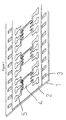
- Figure 1 shows the form of the patterned tape.
- On organic insulating film 1 are the adhesive agent 2 and the conductor pattern 5, and there are provided sprocket holes 3 for feeding the film and device holes 4 in which the devices are set.
- Figure 2 shows in cross-section one embodiment of a TCP type semiconductor device.
- the semiconductor integrated circuit is attached.
- the semiconductor device is produced via a resin sealing process based on sealing resin 9.
- other components are connected to the attached integrated circuit, etc, via outer lead 7, and the TCP type semiconductor device mounted on electronic equipment.
- BGAs ball grid arrays
- CSPs chip scale packages
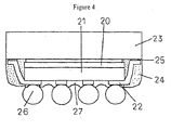
- FIG. 3 and Figure 4 show cross-sections of embodiments of such semiconductor devices (BGA or CSP repectively).
- 12 and 20 denote the organic insulating film
- 13 and 21 the adhesive agent
- 14 and 22 the conductor pattern
- 15 and 23 the semiconductor integrated circuit
- 16 and 24 the sealing resin
- 17 and 25 gold bumps
- 18 and 26 solder balls
- 19 a reinforcing board
- 27 a solder resist.
- the interposer referred to here has the same kind of function as the aforesaid TCP patterned tape, so it is possible to employ the adhesive-backed tape used for TAB.
- This will of course be useful in connection systems having an inner lead, but it is particularly applicable in a process where copper foil is laminated following the mechanical punching of holes for solder balls and device holes for ICs.
- an inner lead is not necessary, and in the process of introducing holes for solder balls and IC device holes along with the copper foil, there may be used a copper clad laminate where the lamination of the copper foil and hot curing of the adhesive have already been carried out.
- the objective of the present invention lies in resolving such problems by improving the properties of the insulating film, such as the polyimide, which constitutes the base film, and to offer an adhesive-backed tape for semiconductors which has outstanding dimensional stability and enables there to be simultaneously achieved both a reduction in warping in the copper-foil-laminated state and in the state following the formation of the circuit pattern; together with a copper clad laminate, a semiconductor connecting substrate and a semiconductor device employing said adhesive-backed tape.
- the insulating film such as the polyimide, which constitutes the base film
- a further objective of the present invention is an adhesive-backed tape for semiconductors which provides both good punchability and retention of adhesive agent modulus of elasticity at high temperatures.
- the present invention relates to an adhesive-backed tape for semiconductors which is characterized in that it is composed of a laminate of an insulating film layer having the following characteristics (1) and (2), and at least one adhesive agent layer in the semi-cured state.
- Figure 1 shows a perspective view of an embodiment of the semiconductor connecting substrate (patterned tape) prior to the mounting of the semiconductor integrated circuits, which is obtained by processing the adhesive-backed tape for semiconductor devices of the present invention.
- FIG. 2 shows a cross-sectional view of an embodiment of a semiconductor device (TCP) using the adhesive-backed tape for semiconductor devices of the present invention.
- Figure 3 shows a cross-sectional view of an embodiment of a semiconductor device (BGA) using the adhesive-backed tape for semiconductor devices of the present invention.
- Figure 4 shows a cross-sectional view of an embodiment of a semiconductor device (CSP) using the adhesive-backed tape for semiconductor devices of the present invention.
- CSP semiconductor device
- the insulating film used in the present invention there are plastics such as polyimides, polyesters, polyphenylene sulphide, polyether sulphones, polyetherether ketones, aramids, polycarbonates, polyarylates and liquid crystal polymers, and also films which comprise a composite material such as a glass cloth impregnated with an epoxy resin. There may also be used a laminate of a plurality of these films.
- films in which the chief component is a polyimide resin are outstanding in their mechanical, electrical, heat resistance and chemical properties, etc, and provide a good balance too in terms of cost, so are favourably employed.
- the insulating film can be subjected to a surface treatment by, for example, a hydrolysis, corona discharge, low temperature plasma, physical roughening or adhesion-enhancing coating treatment, on one or both faces.
- the thickness of the insulating film is preferably 10-65 ⁇ m and more preferably 25-55 ⁇ m. If it is less than 10 ⁇ m, the mechanical strength is low and the usability in the patterning and subsequent stages is impaired, so this is undesirable. If it is more than 65 ⁇ m, it is difficult to reduce the size of solder balls and via holes, so this is undesirable.
- the transverse direction (TD) coefficient of linear expansion of the film is preferably greater than the coefficient of linear expansion of the clad metal foil.
- the coefficient of linear expansion at 50-200°C is preferably 17-30 ppm/°C and more preferably 19-25 ppm/°C in the case where the metal foil is an electrolytic copper foil. If it is less than 17 ppm/°C or more than 30 ppm/°C, then there is considerable warping in the copper-foil-laminated state, which is undesirable.
- the tensile modulus of elasticity in the present invention is the value at 25°C defined by ASTM-D882.
- the tensile modulus of elasticity is preferably 6-12 GPa, and more preferably 7-10 GPa. If it is less than 6 GPa, then the mechanical strength is low and the usability in the patterning and subsequent stages is impaired, which is undesirable. If it is higher than 12 GPa, then the flexibility is lowered which is undesirable.
- the difference between these coefficients of linear expansion is preferably 3-10 ppm/°C, and more preferably 5-7 ppm/°C. If the difference is less than 3 ppm/°C or more than 10 ppm/°C, then in both cases there is considerable warping in the copper-foil-laminated state, which is undesirable.
- the value in the MD be smaller than that in the TD.
- Reference here to the coefficient of linear expansion is the value measured by the TMA tensile loading method, and specifically it is the value given by evaluation method (2) of the examples.
- the percentage heat shrinkage of the insulating film layer at 200°C in the film transverse direction (TD) is preferably 0.0 to 0.2%, and more preferably 0.0 to 0.1%.
- the percentage heat shrinkage influences the warping in the copper-foil-laminated state in the same way as the coefficient of linear expansion, and if it is less than 0.0% or more than 0.2% then in each case there is considerable warping in the copper-foil-laminated state, which is undesirable.
- Reference here to the percentage heat shrinkage means the value measured by a method based on ASTM D1204, and is the value determined by the method given in evaluation method (3) of the examples.
- the humidity coefficient of expansion of the insulating film layer in the film transverse direction (TD) is preferably no more than 23 ppm/°C. More preferably, it is 5 to 20 ppm/°C and still more preferably 5 to 15 ppm/°C.
- the humidity coefficient of expansion affects the warping in the copper-foil-laminated state and if the value exceeds 23 ppm/°C then there is considerable warping in the copper-foil-laminated state, which is undesirable.
- the precise measurement conditions for the humidity coefficient of expansion are given in evaluation method (4) of the examples.
- the water absorption of the insulating film layer is preferably no more than 1.7% and more preferably no more than 1.5%. If the percentage water absorption exceeds 1.7%, the amount of moisture vaporized by the heat of soldering at the time of the semiconductor device mounting is considerable so, for example, separation occurs between structural components of the TAB tape, and the soldering heat resistance is poor.
- the water absorption measurement conditions are given in evaluation method (5) of the examples.
- the thermal conductivity of the insulating film layer is preferably no more than 0.40 W/m.K, and more preferably no more than 0.30 W/m.K. If the thermal conductivity exceeds 0.40 W/m.K, then the heat of soldering is transmitted to the insulating film layer and adhesive agent layer, so that moisture contained in the insulating film layer and in the adhesive agent layer is readily vaporized and caused to expand. As a result, separation occurs between the structural components of the TAB tape and there is poor solder heat resistance.
- the conditions for measuring the thermal conductivity are given in evaluation method (6) of the examples.
- the water vapour transmission of the insulating film layer is preferably at least 0.04 g/m 2 /24hr. If the water vapour transmission is less than 0.04 g/m 2 /24hr, then moisture absorbed by the substrate does not escape when heating at the time of soldering, and there is explosive vaporization and expansion, so that separation of the structural components occurs.
- the conditions for measurement of the water vapour transmission are given in evaluation method (7) of the examples.
- the adhesive agent layer is normally provided in a semi-cured state and its chemical structure is not particularly restricted providing that, following copper foil laminating, curing and crosslinking can be effected by the application of at least one type of energy selected from heat, pressure, an electric field, a magnetic field, ultraviolet light, radiation, ultrasonics or the like.
- the amount of thermosetting resin added is preferably 2 to 20 wt% of the adhesive agent layer and more preferably 4 to 15 wt%.
- the thickness of the adhesive agent layer prior to curing is preferably in the range 3 to 50 ⁇ m.
- the epoxy resins are not especially restricted, providing that they possess two or more epoxy groups per molecule, and examples include the diglycidyl ethers of bisphenol F, bisphenol A, bisphenol S, dihydroxy-naphthalene, dicyclopentadiene diphenol, dicyclopentadiene dixylenol and the like, epoxidized phenolic novolaks, epoxidized cresol novolaks, epoxidized trisphenylol methane, epoxidized tetraphenylol ethane, epoxidized m-xylenediamine, cyclic epoxies and the like.
- phenolic resins there can be used any known phenolic resin such as novolak type phenolic resins or resol type phenolic resins.
- resins comprising phenol, alkyl-substituted phenols such as cresol, p-tert-butylphenol, nonylphenol and p-phenylphenol, terpene, dicyclopentadiene and other such cyclic alkyl-modified phenols, those with a functional group containing a heteroatom such as a nitro group, halogen group, cyano group, amino group or the like, those with a naphthalene, anthracene or similar skeletal structure, and polyfunctional phenols such as bisphenol F, bisphenol A, bisphenol S, resorcinol and pyrogallol.
- polyimide resins there are those obtained by the imidation of polyamic acids obtained by the polycondensation of the dianhydride of an aromatic tetracarboxylic acid such as pyromellitic acid, 3,3',4,4'-biphenyltetracarboxylic acid or 3,3',4,4'-benzophenonetetracarboxylic acid, and a diamine such as 4,4'-diaminodiphenylether, 4,4'-diaminodiphenyl-sulphone, p-phenylenediamine, dimethylbenzidine or 3,3'-diaminobenzophenone.
- aromatic tetracarboxylic acid such as pyromellitic acid, 3,3',4,4'-biphenyltetracarboxylic acid or 3,3',4,4'-benzophenonetetracarboxylic acid
- a diamine such as 4,4'-diaminodiphenylether,
- maleimide resins those which are at least difunctional are preferred, such as N,N'-(4,4'-diphenylmethane)bismaleimide, N,N'-p-phenylenebis-maleimide, N,N'-m-phenylenebismaleimide, N,N'-2,4-tolylenebismaleimide, N,N'-2,6-tolylenebismaleimide, N,N'-ethylenebismaleimide, N,N'-hexamethylenebis-maleimide and the like.
- thermosetting resin curing agents and curing accelerators there are no particular restrictions on the addition of thermosetting resin curing agents and curing accelerators to the adhesive agent layer of the present invention.
- thermosetting resin curing agents and curing accelerators there can be used known materials such as diethylenetriamine, triethylene-tetramine or other such aliphatic polyamines, aromatic polyamines, boron trifluoride triethylamine complex or other such boron trifluoride amine complexes, 2-alkyl-4-methylimidazole, 2-phenyl-4-alkylimidazole or other such imidazole derivative, phthalic anhydride, trimellitic anhydride or other such organic acid, dicyandiamide, triphenylphosphine, diazabicycloundecene or the like.
- the amount added is preferably from 0.1 to 10 parts by weight per 100 parts by weight of the adhesive agent layer.
- antioxidants As well as the above components, there are no restrictions on the addition of antioxidants, ion arrestors or other such organic or inorganic components within a range such that the properties of the adhesive agent are not impaired.
- the adhesive agent layer of the present invention can contain thermoplastic resins.
- Thermoplastic resins are effective for controlling the softening temperature, and have the function of enhancing adhesive strength, flexibility, thermal stress mitigation, and insulation based on lower moisture absorption.
- the amount of thermoplastic resin added is preferably 30-60 wt%, and more preferably 35-55 wt%, of the adhesive agent layer.
- thermoplastic resins are acrylonitrile-butadiene copolymer (NBR), acrylonitrile-butadiene rubber-styrene resin (ABS), styrene-butadiene-ethylene resin (SEBS), acrylics, polyvinyl butyral, polyamides, polyesteramides, polyesters, polyimides, polyamide-imides, polyurethanes and the like.
- these thermoplastic resins may also possess functional groups capable of reacting with the aforesaid phenolic resins, epoxy resins or other thermosetting resins. Specific examples of these groups are amino groups, carboxyl groups, epoxy groups, hydroxyl groups, methylol groups, isocyanate groups, vinyl groups, silanol groups and the like.
- thermoplastic resins polyamide resins are preferred in terms of adhesion to the copper foil, flexibility and insulation properties, and various kinds of polyamide resin can be used.
- Polyamide resins containing, as an essential component, dicarboxylic acid with 36 carbons (so-called dimer acid) are particularly suitable for conferring flexibility on the adhesive agent layer and, because of low moisture absorption, they are outstanding in their insulation properties.
- polyamide resins which are polyamide resins of amine value at least 1 but less than 3 are favourably employed.
- Polyamide resins containing dimer acid are obtained by the polycondensation of a diamine and dimer acid by the usual methods, and in such circumstances, as well as the dimer acid, there may also be included dicarboxylic acid such as adipic acid, azelaic acid or sebacic acid as a copolymer component.
- dicarboxylic acid such as adipic acid, azelaic acid or sebacic acid
- Known diamines such as ethylenediamine, hexamethylenediamine or piperazine can be used, and two or more types may be mixed together from the point of view of moisture absorption, solubility or the like.
- the acid value of the polyamide resin is calculated from the titre using potassium hydroxide. That is to say, 5 g of the polyamide is weighed out and dissolved in 50 ml of a 2:1 solvent mixture of toluene and n-butanol. A few drops of phenolphthalein are added as an indicator and then titration performed using a 0.1 N potassium hydroxide solution in methyl alcohol. The acid value is calculated using the following formula (1) from the amount of potassium hydroxide employed for the titration.
- Av (56.1 x 0.1 x F x (A - B))/50
- the strength of the potassium hydroxide is calculated from the following formula (2) by potassium hydrogen phthalate titration.
- F 1000 x 0.5/(204.22 x (V - b) x 0.1)
- V amount of potassium hydroxide solution required in the titration (ml)
- b amount corresponding to V in a blank test (ml)
- An adhesive agent composed only using polyamide resin of acid value less than 3 is inferior in its punchability.
- the proportion of polyamide resin contained in the adhesive agent layer lies in the range 1 to 90 wt%. If the amount is less than 1 wt%, problems are produced in terms of pliability, and there is a fear that the adhesive agent layer will separate away. With more than 90 wt%, the insulation properties are impaired, so the reliability is reduced. It is further preferred that the amount lies in the range 20-70 wt%.
- the elastic modulus at 150°C of the adhesive agent layer in the film transverse direction (TD) is preferably from 1 MPa to 5 GPa, more preferably from 2 MPa to 1 GPa, and still more preferably from 50 MPa to 1 GPa, and furthermore, the coefficient of linear expansion at 25-150°C in the film transverse direction (TD) is preferably in the range 10-500 ppm/°C and more preferably 20-300°C.
- E' the storage elastic modulus
- the elastic modulus is less than 1 MPa, then there is a lowering of the heat resistance at the time of reflow, which is undesirable. If the elastic modulus is greater than 5 GPa, as well as there being insufficient flexibility, there is considerable warping following the circuit pattern formation, which is undesirable.
- wire bonding temperatures are generally from 110°C to 200°C and taking, as a typical value, the elastic modulus (E' determined by the dynamic viscoelasticity method) at 150°C as an index, this should appropriately lie in the range given above.
- the elastic modulus at 25°C of the adhesive agent layer in the film transverse direction (TD) after curing preferably lies in the range 10 MPa to 5 GPa, and more preferably in the range 100 MPa to 3 GPa. If the elastic modulus is less than 10 MPa, then punching faults arise and the punchability is reduced, so this is undesirable. If the elastic modulus is greater than 5 GPa, then the adhesive strength to the copper foil is reduced, which is undesirable.
- the coefficient of linear expansion in the film transverse direction (TD) at 25-150°C lies in the range 10-500 ppm/°C and more preferably in the range 20-300 ppm/°C. If the coefficient of linear expansion is less than 10 ppm/°C, or greater than 500 ppm/°C, then warping is increased which is undesirable.
- the method of measuring the coefficient of linear expansion is given in evaluation method (9) of the examples.
- the haze value of the adhesive agent layer is preferably no more than 20. If the haze is more than 20, then the wire bonding properties are poor.
- haze refers to the cloudiness and is specified in JIS K7105, but the details are given in evaluation method (10) of the examples.
- the adhesive-backed tape for semiconductor devices of the present invention may have a protective film layer.
- the protective film layer is not particularly restricted providing that it can be peeled away from the adhesive agent surface prior to the hot lamination of the copper foil without adversely affecting the form of the adhesive-backed tape.
- a coating material comprising an aforesaid adhesive agent composition solution dissolved in a solvent is applied onto an insulating film such as a polyimide which meets the requirements of the present invention, and then dried. It is preferred that the application be carried out so that there is formed an adhesive agent layer film thickness of 5 to 125 ⁇ m.
- the drying conditions are preferably 1 to 5 minutes at 100-200°C.
- the solvent is not particularly restricted but a solvent mixture of an aromatic such as toluene or xylene and an alcohol such as methanol or ethanol is favourably employed.
- the compatibility is generally poor and the haze value of the adhesive agent is raised.
- the compatibility is generally poor and the haze value of the adhesive agent is raised.
- a protective film is laminated to the film obtained in this way, and then finally the film is slit to a specified width and the adhesive-backed tape obtained.
- 3-35 ⁇ m electrolytic or rolled copper foil is laminated to the adhesive-backed tape sample from (1) under conditions comprising 110-180°C, 30 N/cm and 1 m/min. Where required, a stepwise hot curing treatment is carried out for 1 to 24 hours at 80-300°C in an air oven and the copper-clad laminate produced. In such circumstances, device holes and solder ball holes may be introduced into the adhesive-backed tape sample prior to the copper-foil cladding.
- an integrated circuit is connected onto the patterned tape from (3) using an epoxy type die-bond material. Furthermore, die bonding is carried out for 3 seconds at 110-250°C on the reverse face and, optionally, the die-bond material is cured. Next, under conditions comprising 110-200°C and 60-110 kHz, wirebonding connection is effected. Finally, by sealing based on an epoxy sealing resin and solder ball connection stages, an FP-BGA type semiconductor device is obtained ( Figure 2).
- the die-bond material there may also be used adhesive tape with 10-100 ⁇ m adhesive agent layers on both faces of an insulating film such as polyimide which satisfies the requirements of the present invention.
- the press bonding onto the patterned tape and the IC press bonding are preferably carried out for about 0.5 to 5 seconds at 80-200°C.
- a stepwise hot curing treatment may be carried out for 1-24 hours at 80-300°C, and the adhesive agent cured.
- the insulating film layer was immersed in water at 23°C for 24 hours, and the change in weight of the insulating film layer before and after immersion measured, and then calculation carried out using the following formula.
- water absorption (%) (weight after immersion - weight before immersion)/weight before immersion
- thermal conductivity (W/m.K) heat diffusivity (m 2 /s) x heat capacity (J/m 3 K)
- the heat diffusivity was measured by cutting out a disc-shaped sample of diameter about 10 mm and thickness 50 ⁇ m, then coating both faces by sputtering platinum, after which both faces were given about a 1 ⁇ m coating with a carbon spray to blacken the faces, and then measurement carried out by the laser flash method at 150°C.
- the heat capacity was calculated from the product of the density and the specific heat.
- the density was measured by the Archimedes method at 23°C.
- the specific heat was measured by DSC (Differential Scanning Calorimetry) at a rate of temperature rise of 10°C/min, and there was employed the specific heat measured at 150°C.
- a film of cured adhesive agent was prepared in the same way as in (8) and used as the test-piece. This was fitted to a TMA device and the dimensional change in the test-piece over the range 25-150°C read-off under conditions of 2 g loading and 20°C/min rate of temperature rise, after which calculation was performed using the following formula.
- linear expansion coefficient (1/°C) (L 1 - L 0 )/L 0 (150 - 25)
- the measurement sample an adhesive agent sheet comprising a PET film of thickness 25 ⁇ m on which had been coated a 12 ⁇ m adhesive agent layer. Furthermore, as a reference sample, there was used the uncoated PET film (25 ⁇ m).
- the diffuse transmittance and the total luminous transmittance were measured. The haze (ratio of diffuse transmittance to total luminous transmittance) for the reference sample was determined and taken as 0 (standard). Next, the diffuse transmittance and total luminous transmittance of the adhesive sheet were measured, and the haze for just the adhesive agent layer alone determined.
- a 20 mm square IC was press bonded onto the patterned tape prepared in (11) using an epoxy die-bonding material ("LE-5000" produced by Lintech), and then hot curing carried out for 30 minutes at 160°C in this state.
- an epoxy die-bonding material ("LE-5000" produced by Lintech)
- resin sealing was performed.
- the solder balls were attached by reflow and the semiconductor device used for evaluation obtained.
- 18 ⁇ m electrolytic copper foil was laminated to the adhesive-backed tape under conditions of 140°C, 30 N/cm and 1 m/min.
- the sample was cut to a width of 35 mm x 200 mm and a sequential curing treatment carried out in an air oven for 4 hours at 80°C, 5 hours at 100°C and 4 hours at 160°C, and the sample used for evaluation of the warping obtained.
- the measurement of warping was carried out after conditioning for 24 hours at 23°C and 55% RH based on SEMI-G76-0299. With one edge of the sample pressed down, using vernier callipers the height on the other side of an upwardly warping sample was measured and this was taken as the amount of warping (where the copper foil curved upwards, this was taken as plus).
- the copper foil side of the warping evaluation sample produced in (13) was subjected to photoresist film formation, etching, resist elimination and electrolytic gold plating, and an evaluation sample produced.
- the area of the adhesive was taken as 100
- the area of the conductor regions was 30.
- the measurement of the warping was carried out in the same way as in (13).
- a round hole (0.3 mm diameter) was introduced from the protective film side into a sample of the adhesive agent sheet with a protective film/adhesive agent layer/organic insulating film structure.
- the protective film had been removed, the condition of the adhesive agent layer at the hole circumference was observed. Where there were splits or gaps in adhesive agent layer, or where there was separation from the organic insulating film, the punchability was regarded as poor.
- polyamide reactants were prepared by adding together mixtures of these acids/amine, antifoaming agent and up to 1% phosphoric acid catalyst. These were subjected to thermal polymerization at 205°C and, following standard procedure, antioxidant then added, after which the polyamide resin was removed.
- the four types of polyamide resin shown in Table 1 were obtained by suitable adjustment of the acid/amine component ratio and the polymerization time.
- polyimide film L was prepared having the properties shown in Table 1.
- Upilex 75S produced by Ube Industries, after polishing with a grinder to an average thickness of 60 ⁇ m.
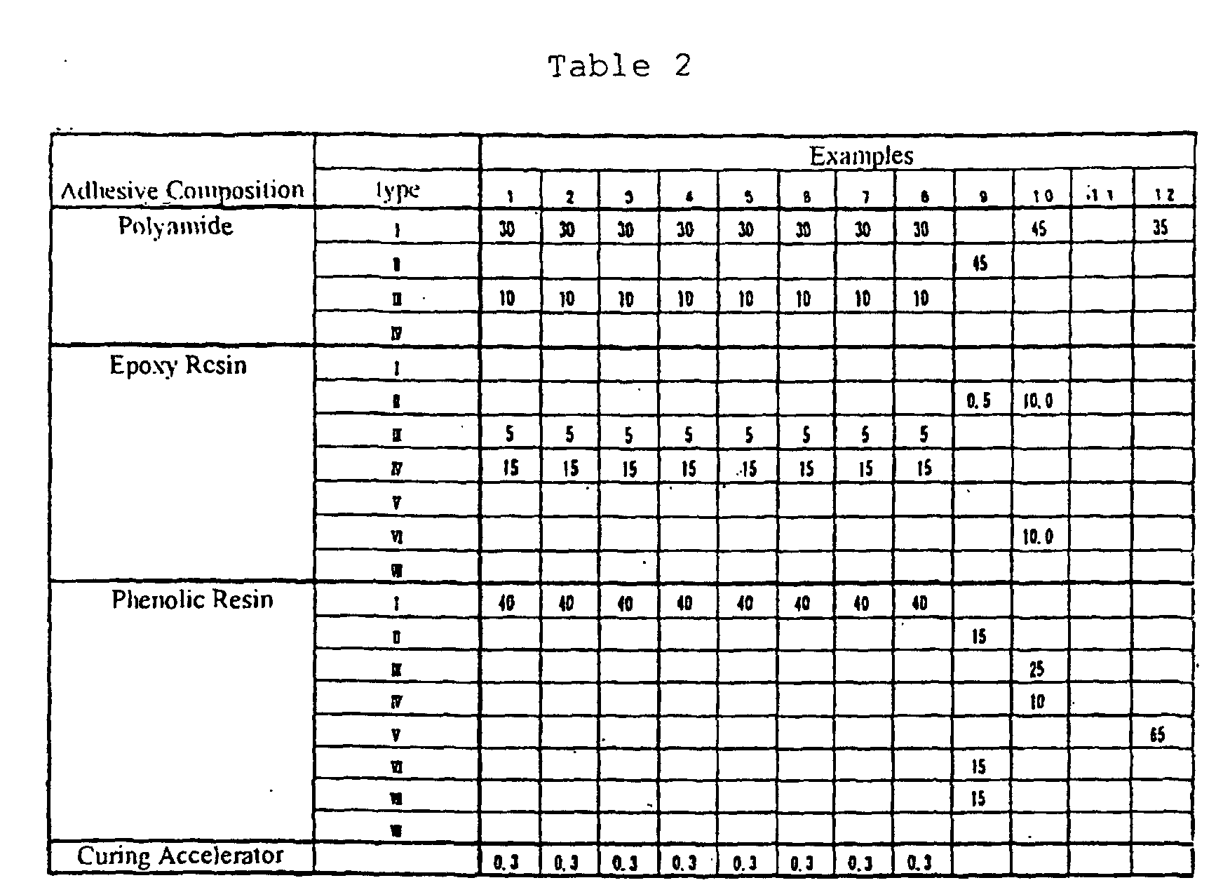
- the polyamide resins prepared in Reference Example 1 and the other starting materials shown in Table 1 were dissolved in the proportions shown in Table 2 in a solvent mixture of methanol/monochlorobenzene at a solids concentration of 20 wt%, and adhesive agent solutions prepared.
- the polyamide resin was stirred for 5 hours at 70°C, then the epoxy resin was added and stirring continued for a further 3 hours.
- the solution temperature was reduced to 30°C and, while stirring, the phenolic resin and curing accelerator were added in turn and stirring carried out for 5 hours, to produce the adhesive agent solution.
- the adhesive agent solution was applied, so as to give a thickness after drying of about 12 ⁇ m, onto polyethylene terephthalate film (Lumirror, produced by Toray Industries) of thickness 25 ⁇ m as a protective film, then drying carried out for 1 minute at 100°C and 5 minutes at 160°C, to prepare adhesive agent sheets I, II, III and V. Furthermore, the adhesive agents sheets obtained were laminated under conditions of 120°C and 0.1 MPa to the polyimide films A-H, K, L and M prepared in Reference Example 2, and to aforesaid films N, I, J, R and S, and also to aramid film O and liquid crystal polymer film P, and adhesive-backed tapes produced.
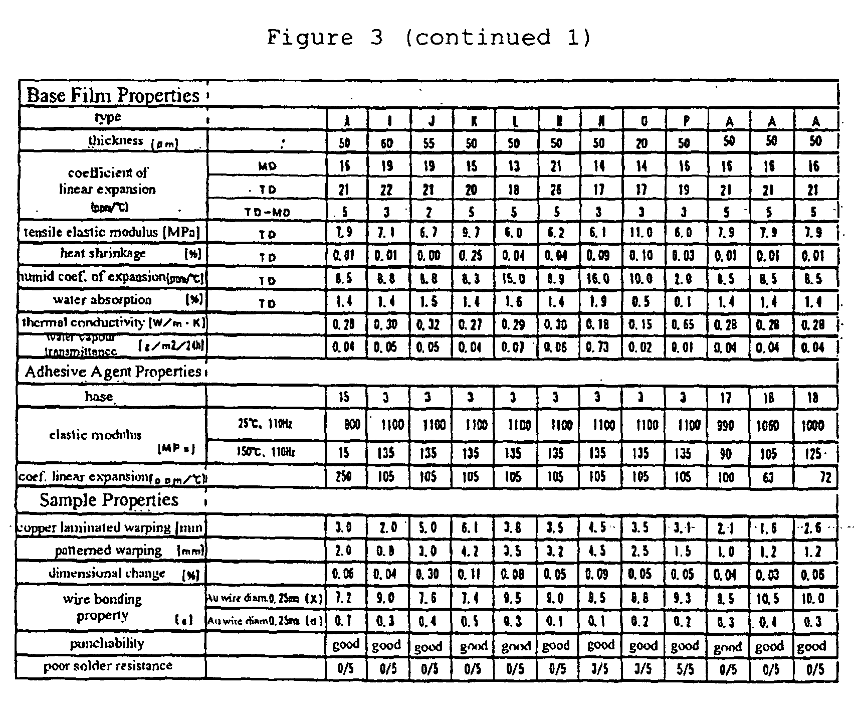
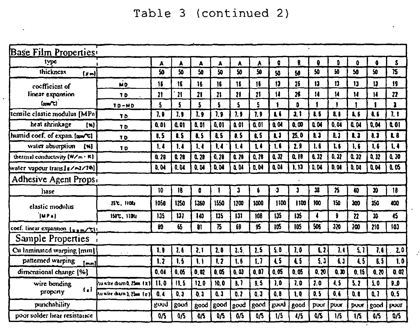
- Tables 3, 4 and 5 show the combinations of adhesive agent sheet and polyimide film, and the properties of the adhesive-backed tapes obtained. Next, by the methods described in aforesaid Evaluation Methods (11) to (16), patterned tape and semiconductor device preparation and evaluation were carried out. The results are shown in Table 3.
- adhesive agent sheet VI was prepared from this adhesive agent solution. Furthermore, using the polyimide film A prepared in Reference Example 2, an adhesive-backed tape, patterned tape and a semiconductor device were prepared by the aforesaid methods. The properties obtained are shown in Table 3.
- the polyamide resins prepared in Reference Example 1 and the other starting materials indicated in Table 1 were dissolved in the proportions shown in Table 2 in a solvent mixture of methanol/monochlorobenzene to give a solids concentration of 20 wt%, and adhesive agent solutions prepared.
- the polyamide resin was stirred for 5 hours at 70°C, then the epoxy resin was added and stirring continued for a further 3 hours.
- the solution temperature was reduced to 30°C and, while stirring, the phenolic resin and curing accelerator were added in turn and stirring carried out for 5 hours, to produce the adhesive agent solution.
- the adhesive agent solution was applied, so as to give a thickness following drying of about 18 ⁇ m, on polyethylene terephthalate film (Lumirror, produced by Toray Industries) of thickness 25 ⁇ m as a protective film, then drying carried out for 1 minute at 100°C and 5 minutes at 160°C, to prepare the adhesive agent sheet.
- polyethylene terephthalate film Limirror, produced by Toray Industries
- the adhesive agent sheet obtained was laminated under identical conditions to the polyimide film A prepared in Reference Example 2, and an adhesive-backed tape produced.
- the properties of the adhesive-backed tape obtained are shown in Table 3.
- a patterned tape and semiconductor device were prepared and evaluated by the aforesaid methods. The results are shown in Table 3.
- the present invention offers, on an industrial basis, an adhesive-backed tape suitable for the production of semiconductor devices where there is employed a film-form adhesive agent such as in the case of the patterned tape used in tape automated bonding (TAB), the semiconductor connecting substrate such as an interposer used for a ball grid array (BGA) package, die bonding materials, lead frame fixing tape, LOC tape, the interlayer adhesive sheets of a multilayer substrate and the like, employed when mounting semiconductor integrated circuits; and to a copper-clad laminate, semiconductor connecting substrate and semiconductor device employing same.
- a film-form adhesive agent such as in the case of the patterned tape used in tape automated bonding (TAB), the semiconductor connecting substrate such as an interposer used for a ball grid array (BGA) package, die bonding materials, lead frame fixing tape, LOC tape, the interlayer adhesive sheets of a multilayer substrate and the like, employed when mounting semiconductor integrated circuits; and to a copper-clad laminate, semiconductor connecting substrate and semiconductor device employing same.
Landscapes
- Adhesive Tapes (AREA)
- Laminated Bodies (AREA)
- Wire Bonding (AREA)
- Adhesives Or Adhesive Processes (AREA)
Abstract
Description
- 1, 12, 20
- insulating film
- 2, 13, 21
- adhesive agent
- 3
- sprocket holes
- 4
- device holes
- 5, 14, 22
- conductor for semiconductor integrated circuit connection
- 6
- inner lead portion
- 7
- outer lead portion
- 8, 15, 23
- semiconductor integrated circuits
- 9, 16, 24
- sealing resin
- 10, 17, 25
- gold bumps
- 11
- protective film
- 18, 26
- solder balls
- 19
- reinforcing board
- 27
- solder resist
| gold wire diameter | 25 µm |
| ultrasonic frequency | 110 KHz |
| bonding temperature | 150°C |
- N:
- There was employed Kapton 200EN produced by Toray-DuPont.
- O:
- There was used 20 µm Micton produced by Toray Industries.
- P:
- There was used 50 µm BIAC produced by Japan Goretex.
- Q:
- There was used Upilex 50S produced by Ube Industries.
- R:
- There was used Kapton 200V produced by Toray-DuPont.
- S:
- There was used Upilex 75S produced by Ube Industries.




Claims (20)
- An adhesive-backed tape for semiconductors which is characterized in that it is composed of a laminate of an insulating film layer having the following characteristics (1) and (2) and at least one adhesive agent layer in the semi-cured state.(1) The coefficient of linear expansion in the film transverse direction (TD) at 50-200°C is 17-30 ppm/°C(2) The tensile modulus of elasticity is 6-12 GPa
- An adhesive-backed tape for semiconductors according to Claim 1 where the coefficient of linear expansion in the film transverse direction (TD) at 50-200°C is 19-25 ppm/°C.
- An adhesive-backed tape for semiconductors according to Claim 1 where the tensile modulus of elasticity is 7-10 GPa.
- An adhesive-backed tape for semiconductors according to Claim 1 where the thickness of the insulating film layer is 10-65 µm.
- An adhesive-backed tape for semiconductor devices according to Claim 1 where the difference in the transverse direction (TD) and machine direction (MD) coefficients of linear expansion of the insulating film layer is 3-10 ppm/°C.
- An adhesive-backed tape for semiconductor devices according to Claim 1 where the humidity coefficient of expansion of the insulating film is no more than 23 ppm/%RH.
- An adhesive-backed tape for semiconductor devices according to Claim 1 where the percentage heat shrinkage of the insulating film layer is 0.0% to 0.2%.
- An adhesive-backed tape for semiconductor devices according to Claim 1 where the water absorption of the insulating film layer is no more than 1.7%.
- An adhesive-backed tape for semiconductor devices according to Claim 1 where the thermal conductivity of the insulating film layer is no more than 0.40 W/m.K.
- An adhesive-backed tape for semiconductor devices according to Claim 1 where the water vapour transmittance of the insulating film layer is at least 0.04 g/m2/24h by conversion to 1 mm of film thickness.
- An adhesive-backed tape for semiconductor devices according to Claim 1 where the chief component of the insulating film layer is polyimide resin.
- An adhesive-backed tape for semiconductor devices according to Claim 1 where the elastic modulus of the adhesive agent layer in the TD at 150°C is 1 MPa-5 GPs and, furthermore, the coefficient of linear expansion at 25-150°C lies in the range 10-500 ppm/°C.
- An adhesive-backed tape for semiconductor devices according to Claim 1 which is characterized in that the haze of the adhesive agent layer is no more than 20.
- An adhesive-backed tape for semiconductor devices according to Claim 13 where the adhesive agent layer contains epoxy resin and at least one type of polyamide resin of acid value at least 3.
- An adhesive-backed tape for semiconductor devices according to Claim 1 where the adhesive agent layer contains at least one type of thermosetting resin selected from epoxy resins, phenolic resins, polyimide resins and maleimide resins.
- An adhesive-backed tape for semiconductor devices according to Claim 1 where the adhesive agent layer contains thermosetting resin and at least one type of thermoplastic resin selected from polyamides, acrylonitrile-butadiene copolymer (NBR), polyesters and polyurethanes.
- A copper-clad laminate which employs an adhesive-backed tape for semiconductors according to Claim 1.
- A semiconductor connecting substrate which employs an adhesive-backed tape for semiconductors according to Claim 1.
- A semiconductor device which employs a copper-clad laminate for semiconductors according to Claim 15.
- A semiconductor device which employs a semiconductor connecting substrate according to Claim 16.
Applications Claiming Priority (3)
| Application Number | Priority Date | Filing Date | Title |
|---|---|---|---|
| JP2000255352A JP4665298B2 (en) | 2000-08-25 | 2000-08-25 | TAPE WITH ADHESIVE FOR SEMICONDUCTOR DEVICE, COPPER-CLAD LAMINATE USING SAME, SEMICONDUCTOR CONNECTION BOARD AND SEMICONDUCTOR DEVICE |
| JP2000255352 | 2000-08-25 | ||
| PCT/JP2001/007183 WO2002017379A1 (en) | 2000-08-25 | 2001-08-22 | Semiconductor joining substrate-use tape with adhesive and copper-clad laminate sheet using it |
Publications (4)
| Publication Number | Publication Date |
|---|---|
| EP1249863A1 true EP1249863A1 (en) | 2002-10-16 |
| EP1249863A8 EP1249863A8 (en) | 2003-01-15 |
| EP1249863A4 EP1249863A4 (en) | 2005-03-16 |
| EP1249863B1 EP1249863B1 (en) | 2007-12-05 |
Family
ID=18744154
Family Applications (1)
| Application Number | Title | Priority Date | Filing Date |
|---|---|---|---|
| EP01958398A Expired - Lifetime EP1249863B1 (en) | 2000-08-25 | 2001-08-22 | Semiconductor joining substrate-use tape with adhesive and copper-clad laminate sheet using it |
Country Status (9)
| Country | Link |
|---|---|
| US (1) | US6982484B2 (en) |
| EP (1) | EP1249863B1 (en) |
| JP (1) | JP4665298B2 (en) |
| KR (1) | KR100602537B1 (en) |
| CN (1) | CN1204611C (en) |
| AT (1) | ATE380393T1 (en) |
| DE (1) | DE60131725T2 (en) |
| TW (1) | TW594891B (en) |
| WO (1) | WO2002017379A1 (en) |
Cited By (1)
| Publication number | Priority date | Publication date | Assignee | Title |
|---|---|---|---|---|
| CN116209237B (en) * | 2022-12-29 | 2023-10-27 | 东莞市富颖电子材料有限公司 | Component dispensing paste and preparation process thereof |
Families Citing this family (25)
| Publication number | Priority date | Publication date | Assignee | Title |
|---|---|---|---|---|
| US20030190466A1 (en) * | 2002-04-03 | 2003-10-09 | Katsuji Nakaba | Adhesive sheet for producing semiconductor devices |
| US7005729B2 (en) * | 2002-04-24 | 2006-02-28 | Intel Corporation | Device packaging using tape automated bonding (TAB) strip bonded to strip carrier frame |
| JP4082242B2 (en) * | 2003-03-06 | 2008-04-30 | ソニー株式会社 | Element transfer method |
| JP3952196B2 (en) * | 2003-06-25 | 2007-08-01 | 信越化学工業株式会社 | Method for producing flexible metal foil polyimide laminate |
| JP4397653B2 (en) * | 2003-08-26 | 2010-01-13 | 日東電工株式会社 | Adhesive sheet for semiconductor device manufacturing |
| US7132158B2 (en) * | 2003-10-22 | 2006-11-07 | Olin Corporation | Support layer for thin copper foil |
| JP4785340B2 (en) * | 2003-11-13 | 2011-10-05 | 三井化学株式会社 | Polyimide metal laminate |
| KR100674907B1 (en) * | 2003-11-26 | 2007-01-26 | 삼성전자주식회사 | Highly reliable stackable semiconductor package |
| JP4576270B2 (en) | 2005-03-29 | 2010-11-04 | 昭和電工株式会社 | Method for manufacturing solder circuit board |
| WO2007007865A1 (en) | 2005-07-11 | 2007-01-18 | Showa Denko K.K. | Method for attachment of solder powder to electronic circuit board and solder-attached electronic circuit board |
| US20090041990A1 (en) * | 2005-09-09 | 2009-02-12 | Showa Denko K.K. | Method for attachment of solder powder to electronic circuit board and soldered electronic circuit board |
| KR100728748B1 (en) * | 2005-12-14 | 2007-06-19 | 삼성전기주식회사 | Embedded printed circuit board manufacturing method |
| JP5029057B2 (en) * | 2007-02-19 | 2012-09-19 | 旭硝子株式会社 | Carrier film for fuel cell manufacturing process |
| US7923373B2 (en) | 2007-06-04 | 2011-04-12 | Micron Technology, Inc. | Pitch multiplication using self-assembling materials |
| JP5467720B2 (en) * | 2007-12-28 | 2014-04-09 | リンテック株式会社 | Adhesive composition, adhesive sheet and method for producing semiconductor device |
| JP5792924B2 (en) * | 2009-04-30 | 2015-10-14 | 住友電気工業株式会社 | Adhesive resin composition, laminate and flexible printed wiring board using the same |
| JP5384443B2 (en) | 2010-07-28 | 2014-01-08 | 日東電工株式会社 | Flip chip type semiconductor back film, dicing tape integrated semiconductor back film, semiconductor device manufacturing method, and flip chip type semiconductor device |
| CN104244586A (en) * | 2013-07-04 | 2014-12-24 | 漳州市福世通电子有限公司 | Method for solidifying copper foil and base material of roll-type IC card circuit board |
| JP6238121B2 (en) * | 2013-10-01 | 2017-11-29 | ローム株式会社 | Semiconductor device |
| CN105739138A (en) * | 2016-04-28 | 2016-07-06 | 京东方科技集团股份有限公司 | Panel, solidifying method of frame sealant and processing method of ultrathin substrate |
| CN111164779B (en) * | 2017-09-29 | 2022-12-02 | 株式会社Lg化学 | Method for encapsulating organic electronic components |
| JP6909171B2 (en) * | 2018-02-12 | 2021-07-28 | 株式会社巴川製紙所 | Adhesive sheet for manufacturing semiconductor devices and manufacturing method of semiconductor devices using it |
| RS67189B1 (en) * | 2018-12-17 | 2025-10-31 | Nippon Steel Corp | Adhesively laminated core for stator and electric motor |
| TWI877132B (en) * | 2019-02-04 | 2025-03-21 | 日商索尼半導體解決方案公司 | Electronic device |
| CN114761338B (en) * | 2020-03-05 | 2024-06-28 | 琳得科株式会社 | Rolling body |
Family Cites Families (23)
| Publication number | Priority date | Publication date | Assignee | Title |
|---|---|---|---|---|
| US4868050A (en) * | 1987-02-27 | 1989-09-19 | Ube Industries, Ltd. | Interleaf-containing, fiber-reinforced epoxy resin prepreg |
| US5365113A (en) * | 1987-06-30 | 1994-11-15 | Hitachi, Ltd. | Semiconductor device |
| DE69318675T2 (en) * | 1992-06-04 | 1999-02-04 | Sumitomo Bakelite Co. Ltd., Tokio/Tokyo | ADHESIVE FILM AND ITS PRODUCTION |
| US5406124A (en) * | 1992-12-04 | 1995-04-11 | Mitsui Toatsu Chemicals, Inc. | Insulating adhesive tape, and lead frame and semiconductor device employing the tape |
| JP2923170B2 (en) * | 1993-05-26 | 1999-07-26 | 日立電線株式会社 | Film with excellent punchability and lead frame using the same |
| JPH07278258A (en) | 1994-04-11 | 1995-10-24 | Hitachi Chem Co Ltd | Thermosetting resin composition, adhesive sheet, metal foil with adhesive, polyimide film, and metal-foil-laminated polyimide film |
| JPH08174659A (en) | 1994-12-22 | 1996-07-09 | Kanegafuchi Chem Ind Co Ltd | Method for manufacturing TAB tape |
| JP2968704B2 (en) | 1995-06-08 | 1999-11-02 | 日本電気株式会社 | Semiconductor device |
| TW340967B (en) * | 1996-02-19 | 1998-09-21 | Toray Industries | An adhesive sheet for a semiconductor to connect with a substrate, and adhesive sticking tape for tab, an adhesive sticking tape for wire bonding connection, a substrate for connecting with a semiconductor and a semiconductor device |
| JP3555381B2 (en) | 1996-04-02 | 2004-08-18 | 東レ株式会社 | Tape with adhesive for semiconductor device, copper-clad laminate using the same, substrate for semiconductor connection, and semiconductor device |
| JPH10138318A (en) * | 1996-09-13 | 1998-05-26 | Ube Ind Ltd | Manufacturing method of multilayer extruded polyimide film |
| JPH10178054A (en) | 1996-10-15 | 1998-06-30 | Toray Ind Inc | Semiconductor integrated circuit connecting substrate, components constituting the same, and semiconductor device |
| US6335571B1 (en) * | 1997-07-21 | 2002-01-01 | Miguel Albert Capote | Semiconductor flip-chip package and method for the fabrication thereof |
| JP3347651B2 (en) | 1997-09-17 | 2002-11-20 | 株式会社巴川製紙所 | Adhesive tape for electronic components |
| US6031068A (en) * | 1997-10-23 | 2000-02-29 | Kanegafuchi Kagaku Kogyo Kabushiki Kaisha | Polyimide composition and base tape for TAB carrier tape and flexible printed circuit board made from said composition |
| JPH11233567A (en) | 1998-02-12 | 1999-08-27 | Toray Ind Inc | Tape with adhesive for semiconductor device, copper-clad laminate using the same, substrate for semiconductor connection, and semiconductor device |
| JP3346265B2 (en) | 1998-02-27 | 2002-11-18 | 宇部興産株式会社 | Aromatic polyimide film and laminate thereof |
| JP3580128B2 (en) * | 1998-04-17 | 2004-10-20 | 宇部興産株式会社 | Manufacturing method of metal foil laminated film |
| JP3531719B2 (en) * | 1998-10-21 | 2004-05-31 | 宇部興産株式会社 | Manufacturing method of polyimide resin molding |
| JP3587291B2 (en) * | 1998-12-01 | 2004-11-10 | 株式会社カネカ | TAB tape |
| JP3815911B2 (en) | 1999-01-11 | 2006-08-30 | 宇部興産株式会社 | Film carrier tape |
| JP3815912B2 (en) * | 1999-01-11 | 2006-08-30 | 宇部興産株式会社 | LOC tape |
| JP2002050718A (en) * | 2000-08-04 | 2002-02-15 | Hitachi Ltd | Semiconductor device |
-
2000
- 2000-08-25 JP JP2000255352A patent/JP4665298B2/en not_active Expired - Lifetime
-
2001
- 2001-08-22 AT AT01958398T patent/ATE380393T1/en not_active IP Right Cessation
- 2001-08-22 DE DE60131725T patent/DE60131725T2/en not_active Expired - Fee Related
- 2001-08-22 KR KR1020027005242A patent/KR100602537B1/en not_active Expired - Fee Related
- 2001-08-22 CN CNB018031447A patent/CN1204611C/en not_active Expired - Fee Related
- 2001-08-22 US US10/111,302 patent/US6982484B2/en not_active Expired - Fee Related
- 2001-08-22 WO PCT/JP2001/007183 patent/WO2002017379A1/en not_active Ceased
- 2001-08-22 EP EP01958398A patent/EP1249863B1/en not_active Expired - Lifetime
- 2001-08-22 TW TW090120598A patent/TW594891B/en not_active IP Right Cessation
Cited By (1)
| Publication number | Priority date | Publication date | Assignee | Title |
|---|---|---|---|---|
| CN116209237B (en) * | 2022-12-29 | 2023-10-27 | 东莞市富颖电子材料有限公司 | Component dispensing paste and preparation process thereof |
Also Published As
| Publication number | Publication date |
|---|---|
| WO2002017379A1 (en) | 2002-02-28 |
| EP1249863A4 (en) | 2005-03-16 |
| KR100602537B1 (en) | 2006-07-20 |
| US20030031867A1 (en) | 2003-02-13 |
| KR20020044569A (en) | 2002-06-15 |
| HK1051441A1 (en) | 2003-08-01 |
| CN1393033A (en) | 2003-01-22 |
| EP1249863B1 (en) | 2007-12-05 |
| DE60131725T2 (en) | 2008-11-06 |
| ATE380393T1 (en) | 2007-12-15 |
| TW594891B (en) | 2004-06-21 |
| JP2002076062A (en) | 2002-03-15 |
| DE60131725D1 (en) | 2008-01-17 |
| CN1204611C (en) | 2005-06-01 |
| EP1249863A8 (en) | 2003-01-15 |
| JP4665298B2 (en) | 2011-04-06 |
| US6982484B2 (en) | 2006-01-03 |
Similar Documents
| Publication | Publication Date | Title |
|---|---|---|
| EP1249863B1 (en) | Semiconductor joining substrate-use tape with adhesive and copper-clad laminate sheet using it | |
| JP4591444B2 (en) | Multilayer film with metal layer and semiconductor device | |
| EP1447843B1 (en) | Adhesive-backed tape for TAB and semiconductor device | |
| JP2002069270A (en) | Flame retardant non-halogen epoxy resin composition and use thereof | |
| JP2001115127A (en) | Electrically conductive adhesive and wiring board using the same | |
| JP2006176764A (en) | Adhesive composition for electronic device, adhesive sheet for electronic device, electronic component using the same, and electronic device | |
| JPH10335534A (en) | Tape with adhesive for wire bonding connection, copper-clad laminate using the same, substrate for semiconductor connection, and semiconductor device | |
| JP2004031931A (en) | Tape with adhesive for semiconductor device, copper-clad laminate using the same, substrate for semiconductor connection, and semiconductor device | |
| JP5286679B2 (en) | Adhesive composition for electronic parts and adhesive sheet for electronic parts using the same | |
| JP2007116134A (en) | Semiconductor tape, semiconductor adhesive tape, semiconductor integrated circuit connection substrate and semiconductor device | |
| JP3560064B2 (en) | TAB tape with adhesive | |
| JPH10178054A (en) | Semiconductor integrated circuit connecting substrate, components constituting the same, and semiconductor device | |
| JP3750669B2 (en) | Adhesive tape for surface mount BGA type semiconductor device, copper-clad laminate using the same, semiconductor connection substrate and semiconductor device | |
| JP2003092378A (en) | Tape with adhesive for semiconductor device, copper-clad laminate using the same, substrate for semiconductor connection, and semiconductor device | |
| JP3304479B2 (en) | TAB adhesive tape | |
| JP2002285110A (en) | Tape with adhesive for semiconductor device, copper-clad laminate using the same, substrate for semiconductor connection, and semiconductor device | |
| JP2009090605A (en) | Base material having resin, and copper foil having resin | |
| JP3693011B2 (en) | Laminated film and method for producing the same | |
| JPH11233567A (en) | Tape with adhesive for semiconductor device, copper-clad laminate using the same, substrate for semiconductor connection, and semiconductor device | |
| JP2006273996A (en) | Tape with adhesive for semiconductor, copper-clad laminate using the same, substrate for connecting semiconductor integrated circuit, and semiconductor device | |
| JP2003243459A (en) | Adhesive tape and method of manufacturing the same | |
| JP2001250848A (en) | Tape with adhesive for semiconductor device, copper-clad laminate using the same, substrate for semiconductor connection, and semiconductor device | |
| JPH05291356A (en) | Tape for tab | |
| JPH10173008A (en) | TAB adhesive tape, TAB tape and semiconductor device | |
| HK1051441B (en) | Semiconductor joining substrate-use tape with adhesive and copper-clad laminate sheet using it |
Legal Events
| Date | Code | Title | Description |
|---|---|---|---|
| PUAI | Public reference made under article 153(3) epc to a published international application that has entered the european phase |
Free format text: ORIGINAL CODE: 0009012 |
|
| 17P | Request for examination filed |
Effective date: 20020516 |
|
| AK | Designated contracting states |
Kind code of ref document: A1 Designated state(s): AT BE CH CY DE DK ES FI FR GB GR IE IT LI LU MC NL PT SE TR |
|
| RIN1 | Information on inventor provided before grant (corrected) |
Inventor name: KAMEI, RYUICHI Inventor name: TOKUNAGA, MASAMI Inventor name: KIGOSHI, SYOUJI Inventor name: SHIMIZU, KEN Inventor name: TSUTSUMI, YASUAKI Inventor name: OGURA, MIKIHIRO |
|
| A4 | Supplementary search report drawn up and despatched |
Effective date: 20050128 |
|
| 17Q | First examination report despatched |
Effective date: 20050624 |
|
| GRAP | Despatch of communication of intention to grant a patent |
Free format text: ORIGINAL CODE: EPIDOSNIGR1 |
|
| GRAS | Grant fee paid |
Free format text: ORIGINAL CODE: EPIDOSNIGR3 |
|
| GRAA | (expected) grant |
Free format text: ORIGINAL CODE: 0009210 |
|
| AK | Designated contracting states |
Kind code of ref document: B1 Designated state(s): AT BE CH CY DE DK ES FI FR GB GR IE IT LI LU MC NL PT SE TR |
|
| REG | Reference to a national code |
Ref country code: GB Ref legal event code: FG4D |
|
| REG | Reference to a national code |
Ref country code: IE Ref legal event code: FG4D |
|
| REG | Reference to a national code |
Ref country code: CH Ref legal event code: EP |
|
| REF | Corresponds to: |
Ref document number: 60131725 Country of ref document: DE Date of ref document: 20080117 Kind code of ref document: P |
|
| PG25 | Lapsed in a contracting state [announced via postgrant information from national office to epo] |
Ref country code: LI Free format text: LAPSE BECAUSE OF FAILURE TO SUBMIT A TRANSLATION OF THE DESCRIPTION OR TO PAY THE FEE WITHIN THE PRESCRIBED TIME-LIMIT Effective date: 20071205 Ref country code: SE Free format text: LAPSE BECAUSE OF FAILURE TO SUBMIT A TRANSLATION OF THE DESCRIPTION OR TO PAY THE FEE WITHIN THE PRESCRIBED TIME-LIMIT Effective date: 20080305 Ref country code: CH Free format text: LAPSE BECAUSE OF FAILURE TO SUBMIT A TRANSLATION OF THE DESCRIPTION OR TO PAY THE FEE WITHIN THE PRESCRIBED TIME-LIMIT Effective date: 20071205 Ref country code: NL Free format text: LAPSE BECAUSE OF FAILURE TO SUBMIT A TRANSLATION OF THE DESCRIPTION OR TO PAY THE FEE WITHIN THE PRESCRIBED TIME-LIMIT Effective date: 20071205 Ref country code: ES Free format text: LAPSE BECAUSE OF FAILURE TO SUBMIT A TRANSLATION OF THE DESCRIPTION OR TO PAY THE FEE WITHIN THE PRESCRIBED TIME-LIMIT Effective date: 20080316 |
|
| PG25 | Lapsed in a contracting state [announced via postgrant information from national office to epo] |
Ref country code: FI Free format text: LAPSE BECAUSE OF FAILURE TO SUBMIT A TRANSLATION OF THE DESCRIPTION OR TO PAY THE FEE WITHIN THE PRESCRIBED TIME-LIMIT Effective date: 20071205 |
|
| NLV1 | Nl: lapsed or annulled due to failure to fulfill the requirements of art. 29p and 29m of the patents act | ||
| REG | Reference to a national code |
Ref country code: CH Ref legal event code: PL |
|
| PG25 | Lapsed in a contracting state [announced via postgrant information from national office to epo] |
Ref country code: AT Free format text: LAPSE BECAUSE OF FAILURE TO SUBMIT A TRANSLATION OF THE DESCRIPTION OR TO PAY THE FEE WITHIN THE PRESCRIBED TIME-LIMIT Effective date: 20071205 |
|
| ET | Fr: translation filed | ||
| PG25 | Lapsed in a contracting state [announced via postgrant information from national office to epo] |
Ref country code: BE Free format text: LAPSE BECAUSE OF FAILURE TO SUBMIT A TRANSLATION OF THE DESCRIPTION OR TO PAY THE FEE WITHIN THE PRESCRIBED TIME-LIMIT Effective date: 20071205 |
|
| PG25 | Lapsed in a contracting state [announced via postgrant information from national office to epo] |
Ref country code: PT Free format text: LAPSE BECAUSE OF FAILURE TO SUBMIT A TRANSLATION OF THE DESCRIPTION OR TO PAY THE FEE WITHIN THE PRESCRIBED TIME-LIMIT Effective date: 20080505 |
|
| PLBE | No opposition filed within time limit |
Free format text: ORIGINAL CODE: 0009261 |
|
| STAA | Information on the status of an ep patent application or granted ep patent |
Free format text: STATUS: NO OPPOSITION FILED WITHIN TIME LIMIT |
|
| PG25 | Lapsed in a contracting state [announced via postgrant information from national office to epo] |
Ref country code: DK Free format text: LAPSE BECAUSE OF FAILURE TO SUBMIT A TRANSLATION OF THE DESCRIPTION OR TO PAY THE FEE WITHIN THE PRESCRIBED TIME-LIMIT Effective date: 20071205 |
|
| PGFP | Annual fee paid to national office [announced via postgrant information from national office to epo] |
Ref country code: DE Payment date: 20080626 Year of fee payment: 8 |
|
| 26N | No opposition filed |
Effective date: 20080908 |
|
| PG25 | Lapsed in a contracting state [announced via postgrant information from national office to epo] |
Ref country code: GR Free format text: LAPSE BECAUSE OF FAILURE TO SUBMIT A TRANSLATION OF THE DESCRIPTION OR TO PAY THE FEE WITHIN THE PRESCRIBED TIME-LIMIT Effective date: 20080306 |
|
| PG25 | Lapsed in a contracting state [announced via postgrant information from national office to epo] |
Ref country code: MC Free format text: LAPSE BECAUSE OF NON-PAYMENT OF DUE FEES Effective date: 20080831 |
|
| GBPC | Gb: european patent ceased through non-payment of renewal fee |
Effective date: 20080822 |
|
| PG25 | Lapsed in a contracting state [announced via postgrant information from national office to epo] |
Ref country code: IE Free format text: LAPSE BECAUSE OF NON-PAYMENT OF DUE FEES Effective date: 20080822 Ref country code: CY Free format text: LAPSE BECAUSE OF FAILURE TO SUBMIT A TRANSLATION OF THE DESCRIPTION OR TO PAY THE FEE WITHIN THE PRESCRIBED TIME-LIMIT Effective date: 20071205 |
|
| PGFP | Annual fee paid to national office [announced via postgrant information from national office to epo] |
Ref country code: FR Payment date: 20090814 Year of fee payment: 9 |
|
| PG25 | Lapsed in a contracting state [announced via postgrant information from national office to epo] |
Ref country code: GB Free format text: LAPSE BECAUSE OF NON-PAYMENT OF DUE FEES Effective date: 20080822 |
|
| PG25 | Lapsed in a contracting state [announced via postgrant information from national office to epo] |
Ref country code: DE Free format text: LAPSE BECAUSE OF NON-PAYMENT OF DUE FEES Effective date: 20100302 Ref country code: LU Free format text: LAPSE BECAUSE OF NON-PAYMENT OF DUE FEES Effective date: 20080822 |
|
| PG25 | Lapsed in a contracting state [announced via postgrant information from national office to epo] |
Ref country code: TR Free format text: LAPSE BECAUSE OF FAILURE TO SUBMIT A TRANSLATION OF THE DESCRIPTION OR TO PAY THE FEE WITHIN THE PRESCRIBED TIME-LIMIT Effective date: 20071205 |
|
| PG25 | Lapsed in a contracting state [announced via postgrant information from national office to epo] |
Ref country code: IT Free format text: LAPSE BECAUSE OF NON-PAYMENT OF DUE FEES Effective date: 20080831 |
|
| REG | Reference to a national code |
Ref country code: FR Ref legal event code: ST Effective date: 20110502 |
|
| PG25 | Lapsed in a contracting state [announced via postgrant information from national office to epo] |
Ref country code: FR Free format text: LAPSE BECAUSE OF NON-PAYMENT OF DUE FEES Effective date: 20100831 |