EP1240809B1 - Mehrschichtleiterplatte - Google Patents
Mehrschichtleiterplatte Download PDFInfo
- Publication number
- EP1240809B1 EP1240809B1 EP00990013A EP00990013A EP1240809B1 EP 1240809 B1 EP1240809 B1 EP 1240809B1 EP 00990013 A EP00990013 A EP 00990013A EP 00990013 A EP00990013 A EP 00990013A EP 1240809 B1 EP1240809 B1 EP 1240809B1
- Authority
- EP
- European Patent Office
- Prior art keywords
- layer
- thermal expansion
- board
- thin glass
- thickness
- Prior art date
- Legal status (The legal status is an assumption and is not a legal conclusion. Google has not performed a legal analysis and makes no representation as to the accuracy of the status listed.)
- Expired - Lifetime
Links
Images
Classifications
-
- H—ELECTRICITY
- H05—ELECTRIC TECHNIQUES NOT OTHERWISE PROVIDED FOR
- H05K—PRINTED CIRCUITS; CASINGS OR CONSTRUCTIONAL DETAILS OF ELECTRIC APPARATUS; MANUFACTURE OF ASSEMBLAGES OF ELECTRICAL COMPONENTS
- H05K1/00—Printed circuits
- H05K1/02—Details
- H05K1/03—Use of materials for the substrate
Definitions
- the invention relates to a method for producing a Multi-layer circuit board for assembly with electronic components that has at least one layer whose thermal expansion behavior approximately the thermal expansion behavior of the electronic components corresponds and at the same time essentially the thermal expansion behavior of the Multi-layer circuit board determined.
- the dimensional stability (constant dimensions) is particularly important Printed circuit board very important when exposed to temperature.
- thermal Expansion coefficient viewed ⁇ .
- This coefficient of expansion is for Circuit board substrates in FR 4 quality (glass fiber fabric / epoxy resin) 16-18 ppm / K.
- the expansion coefficient for Si chips is 3 ppm / K.
- Typical problems are the differences in the expansion coefficients of epoxy resin glass fabric as the base material for printed circuit boards with assembled silicon bare chips or SMD components.
- the differences between the Coefficient of linear expansion in the z direction in the epoxy resin glass fabric at Soldering process lead to cracks in the hole metallization.
- the first option is not available for area connections and the second represents an additional difficult process step.
- a multilayer printed circuit board can be found in US Pat. No. 4,939,021 Copper layers and the thermal expansion behavior of the Multi-layer circuit board determining between the copper layers provides glass ceramic layers.
- To manufacture such Multilayer printed circuit board is each a powdered glass ceramic mixture under Added a binder between two copper plates.
- a sintering process in which the multilayer printed circuit board arrangement Temperature is exposed to at least the softening temperature of copper must not exceed, however, in which a crystallization or Polycrystallization process to form a sintered glass ceramic can take place. Further It is important to ensure that any suitable process temperature selection Volatiles of the introduced binder should volatilize.
- JP 07 249847 describes a method for producing a multilayer printed circuit board described for equipping with electronic components, which for reasons of Stabilization against different thermal expansion behavior of the individual layers provides a layer of glass fiber material, which by means of a Epoxy resin with another layer material by pressing into a laminate is decreed.
- the process for producing a Multi-layer circuit board for assembly with electronic components that has at least one layer whose thermal expansion behavior approximately the thermal expansion behavior of the electronic components corresponds and at the same time essentially the thermal expansion behavior of the Multi-layer printed circuit board determines that one as a borosilicate glass layer trained thin glass film with a thickness between 30 microns and 1100 microns a resin formulation with a further layer material of Multilayer printed circuit board by pressing into a laminate.
- Suitable thin glass films are, for example, under the type designation AF45 and D263 are available from the German company DESAG. Such thin glass films are borosilicate glass layers with a typical layer thickness between 30 ⁇ m and 1.1 mm. However, thin glass foils are preferably suitable aforementioned purpose with film thicknesses between 50 and 500 microns.
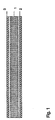
- a 100 ⁇ m thick glass film (1) was used together with a special Resin formulation (2) based on epoxy resin and an 18 ⁇ m thick copper foil (3) a laminate is produced by pressing.
- the laminate has a total thickness of 160 ⁇ m.
- the expansion of the laminate was determined by means of thermomechanical analysis (TMA) measured under constant load (100 mN) depending on temperature. The heating rate was 10 ° C / min.
Landscapes
- Engineering & Computer Science (AREA)
- Microelectronics & Electronic Packaging (AREA)
- Production Of Multi-Layered Print Wiring Board (AREA)
- Laminated Bodies (AREA)
- Reinforced Plastic Materials (AREA)
- Structure Of Printed Boards (AREA)
Applications Claiming Priority (3)
| Application Number | Priority Date | Filing Date | Title |
|---|---|---|---|
| DE19961842 | 1999-12-21 | ||
| DE19961842A DE19961842B4 (de) | 1999-12-21 | 1999-12-21 | Mehrschichtleiterplatte |
| PCT/EP2000/013121 WO2001047326A1 (de) | 1999-12-21 | 2000-12-21 | Mehrschichtleiterplatte |
Publications (2)
| Publication Number | Publication Date |
|---|---|
| EP1240809A1 EP1240809A1 (de) | 2002-09-18 |
| EP1240809B1 true EP1240809B1 (de) | 2003-06-11 |
Family
ID=7933689
Family Applications (1)
| Application Number | Title | Priority Date | Filing Date |
|---|---|---|---|
| EP00990013A Expired - Lifetime EP1240809B1 (de) | 1999-12-21 | 2000-12-21 | Mehrschichtleiterplatte |
Country Status (9)
Families Citing this family (29)
| Publication number | Priority date | Publication date | Assignee | Title |
|---|---|---|---|---|
| DE10145190A1 (de) * | 2001-09-13 | 2003-04-03 | Siemens Ag | Verfahren zur Herstellung glasbasierter elektronischer Bauelemente |
| US7608789B2 (en) | 2004-08-12 | 2009-10-27 | Epcos Ag | Component arrangement provided with a carrier substrate |
| DE102005008512B4 (de) | 2005-02-24 | 2016-06-23 | Epcos Ag | Elektrisches Modul mit einem MEMS-Mikrofon |
| DE102005008514B4 (de) * | 2005-02-24 | 2019-05-16 | Tdk Corporation | Mikrofonmembran und Mikrofon mit der Mikrofonmembran |
| DE102005008511B4 (de) | 2005-02-24 | 2019-09-12 | Tdk Corporation | MEMS-Mikrofon |
| DE102005053767B4 (de) | 2005-11-10 | 2014-10-30 | Epcos Ag | MEMS-Mikrofon, Verfahren zur Herstellung und Verfahren zum Einbau |
| DE102005053765B4 (de) | 2005-11-10 | 2016-04-14 | Epcos Ag | MEMS-Package und Verfahren zur Herstellung |
| WO2013042752A1 (ja) * | 2011-09-22 | 2013-03-28 | 日立化成株式会社 | 積層体、積層板、多層積層板、プリント配線板及び積層板の製造方法 |
| US9050780B2 (en) | 2011-09-22 | 2015-06-09 | Hitachi Chemical Company, Ltd. | Laminate body, laminate plate, multilayer laminate plate, printed wiring board, and method for manufacture of laminate plate |
| US9101061B2 (en) | 2011-09-22 | 2015-08-04 | Hitachi Chemical Company, Ltd. | Laminate body, laminate plate, multilayer laminate plate, printed wiring board, and method for manufacture of laminate plate |
| JPWO2013042750A1 (ja) * | 2011-09-22 | 2015-03-26 | 日立化成株式会社 | 積層体、積層板、多層積層板、プリント配線板及び積層板の製造方法 |
| JPWO2013042751A1 (ja) * | 2011-09-22 | 2015-03-26 | 日立化成株式会社 | 積層体、積層板、多層積層板、プリント配線板及び積層板の製造方法 |
| US20130180760A1 (en) * | 2011-09-22 | 2013-07-18 | Hitachi Chemical Company, Ltd. | Laminate body, laminate plate, multilayer laminate plate, printed wiring board, and method for manufacture of laminate plate |
| KR20140063710A (ko) | 2011-09-22 | 2014-05-27 | 히타치가세이가부시끼가이샤 | 적층체, 적층판, 다층 적층판, 프린트 배선판 및 적층판의 제조 방법 |
| KR102264708B1 (ko) * | 2011-09-22 | 2021-06-11 | 쇼와덴코머티리얼즈가부시끼가이샤 | 적층체, 적층판, 다층 적층판, 프린트 배선판 및 적층판의 제조 방법 |
| CN102548199A (zh) * | 2011-12-29 | 2012-07-04 | 广东生益科技股份有限公司 | 电路基板及其制作方法 |
| US9744745B2 (en) | 2011-12-29 | 2017-08-29 | Shengyi Technology Co., Ltd. | Circuit substrate and manufacturing method thereof |
| US20140377534A1 (en) * | 2011-12-29 | 2014-12-25 | Shengyi Technology Co., Ltd. | Circuit substrate and manufacturing method thereof |
| CN102548200A (zh) * | 2011-12-29 | 2012-07-04 | 广东生益科技股份有限公司 | 电路基板及其制作方法 |
| JP6269506B2 (ja) * | 2012-12-18 | 2018-01-31 | 日立化成株式会社 | 積層体、積層板、プリント配線板、積層体の製造方法、及び積層板の製造方法 |
| CN103129090B (zh) * | 2013-01-30 | 2016-05-25 | 广东生益科技股份有限公司 | 一种玻璃膜基覆铜板的制备方法及其所制得的覆铜板 |
| JPWO2014157468A1 (ja) * | 2013-03-27 | 2017-02-16 | 日立化成株式会社 | 積層体、積層板、プリント配線板、及び積層体、積層板の製造方法 |
| JP6314337B2 (ja) * | 2013-03-28 | 2018-04-25 | 味の素株式会社 | シート材 |
| DE102013106353B4 (de) * | 2013-06-18 | 2018-06-28 | Tdk Corporation | Verfahren zum Aufbringen einer strukturierten Beschichtung auf ein Bauelement |
| KR101650938B1 (ko) * | 2014-09-25 | 2016-08-24 | 코닝정밀소재 주식회사 | 집적회로 패키지용 기판 |
| JP2016221953A (ja) * | 2015-06-03 | 2016-12-28 | 日立化成株式会社 | 積層体の製造方法及び配線板の製造方法 |
| US10459160B2 (en) | 2017-01-31 | 2019-10-29 | Corning Optical Communications LLC | Glass waveguide assemblies for OE-PCBs and methods of forming OE-PCBs |
| JPWO2019208402A1 (ja) * | 2018-04-24 | 2021-05-13 | 三菱瓦斯化学株式会社 | 積層板、プリント配線板、多層プリント配線板、積層体、及び、積層板の製造方法 |
| DE102024208645A1 (de) * | 2024-09-11 | 2025-08-07 | Schaeffler Technologies AG & Co. KG | Leiterplatte und Verfahren zum Herstellen einer solchen |
Family Cites Families (22)
| Publication number | Priority date | Publication date | Assignee | Title |
|---|---|---|---|---|
| US4318954A (en) * | 1981-02-09 | 1982-03-09 | Boeing Aerospace Company | Printed wiring board substrates for ceramic chip carriers |
| US4491622A (en) * | 1982-04-19 | 1985-01-01 | Olin Corporation | Composites of glass-ceramic to metal seals and method of making the same |
| US4812792A (en) * | 1983-12-22 | 1989-03-14 | Trw Inc. | High-frequency multilayer printed circuit board |
| US4609586A (en) * | 1984-08-02 | 1986-09-02 | The Boeing Company | Thermally conductive printed wiring board laminate |
| EP0196865B1 (en) * | 1985-03-27 | 1990-09-12 | Ibiden Co, Ltd. | Electronic circuit substrates |
| JPS63107095A (ja) * | 1986-10-23 | 1988-05-12 | 富士通株式会社 | 多層セラミツク回路基板 |
| CA1306513C (fr) * | 1987-08-18 | 1992-08-18 | Eric Verna | Procede pour terminer une soudure fermee au plasma d'arc avec trou traversant |
| JP2586423B2 (ja) * | 1988-05-26 | 1997-02-26 | 日本電装株式会社 | 混成集積回路 |
| US5073840A (en) * | 1988-10-06 | 1991-12-17 | Microlithics Corporation | Circuit board with coated metal support structure and method for making same |
| JPH0582929A (ja) * | 1991-09-24 | 1993-04-02 | Ibiden Co Ltd | セラミツクス・樹脂複合配線基板 |
| JPH0590720A (ja) * | 1991-09-27 | 1993-04-09 | Ibiden Co Ltd | 複合プリント配線板 |
| JPH05175625A (ja) * | 1991-12-25 | 1993-07-13 | Ibiden Co Ltd | 複合プリント配線板とその製造方法 |
| US5306571A (en) * | 1992-03-06 | 1994-04-26 | Bp Chemicals Inc., Advanced Materials Division | Metal-matrix-composite |
| DE59309575D1 (de) * | 1992-06-15 | 1999-06-17 | Heinze Dyconex Patente | Verfahren zur herstellung von leiterplatten unter verwendung eines halbzeuges mit extrem dichter verdrahtung für die signalführung |
| JPH07249847A (ja) * | 1994-03-14 | 1995-09-26 | Mitsubishi Electric Corp | 低熱膨張プリント配線板 |
| US5571608A (en) * | 1994-07-15 | 1996-11-05 | Dell Usa, L.P. | Apparatus and method of making laminate an embedded conductive layer |
| JPH08181443A (ja) * | 1994-12-21 | 1996-07-12 | Murata Mfg Co Ltd | セラミック多層基板およびその製造方法 |
| US5687062A (en) * | 1996-02-20 | 1997-11-11 | Heat Technology, Inc. | High-thermal conductivity circuit board |
| JPH09270573A (ja) * | 1996-03-29 | 1997-10-14 | Cmk Corp | プリント配線板及びその製造方法 |
| US6136733A (en) * | 1997-06-13 | 2000-10-24 | International Business Machines Corporation | Method for reducing coefficient of thermal expansion in chip attach packages |
| US6287674B1 (en) * | 1997-10-24 | 2001-09-11 | Agfa-Gevaert | Laminate comprising a thin borosilicate glass substrate as a constituting layer |
| US6197418B1 (en) * | 1998-12-21 | 2001-03-06 | Agfa-Gevaert, N.V. | Electroconductive glass laminate |
-
1999
- 1999-12-21 DE DE19961842A patent/DE19961842B4/de not_active Expired - Lifetime
-
2000
- 2000-12-21 AU AU26759/01A patent/AU2675901A/en not_active Abandoned
- 2000-12-21 EP EP00990013A patent/EP1240809B1/de not_active Expired - Lifetime
- 2000-12-21 CN CNB008174733A patent/CN1284424C/zh not_active Expired - Fee Related
- 2000-12-21 AT AT00990013T patent/ATE242954T1/de active
- 2000-12-21 JP JP2001547927A patent/JP4657554B2/ja not_active Expired - Fee Related
- 2000-12-21 CA CA002395080A patent/CA2395080C/en not_active Expired - Lifetime
- 2000-12-21 DE DE50002562T patent/DE50002562D1/de not_active Expired - Lifetime
- 2000-12-21 WO PCT/EP2000/013121 patent/WO2001047326A1/de active IP Right Grant
-
2002
- 2002-06-19 US US10/173,625 patent/US20030010530A1/en not_active Abandoned
-
2003
- 2003-08-27 US US10/648,331 patent/US20040037950A1/en not_active Abandoned
Also Published As
| Publication number | Publication date |
|---|---|
| JP4657554B2 (ja) | 2011-03-23 |
| WO2001047326A1 (de) | 2001-06-28 |
| DE19961842A1 (de) | 2001-07-12 |
| CA2395080C (en) | 2006-10-17 |
| CA2395080A1 (en) | 2001-06-28 |
| EP1240809A1 (de) | 2002-09-18 |
| DE50002562D1 (de) | 2003-07-17 |
| DE19961842B4 (de) | 2008-01-31 |
| US20040037950A1 (en) | 2004-02-26 |
| AU2675901A (en) | 2001-07-03 |
| CN1413427A (zh) | 2003-04-23 |
| US20030010530A1 (en) | 2003-01-16 |
| ATE242954T1 (de) | 2003-06-15 |
| JP2004512667A (ja) | 2004-04-22 |
| CN1284424C (zh) | 2006-11-08 |
Similar Documents
| Publication | Publication Date | Title |
|---|---|---|
| EP1240809B1 (de) | Mehrschichtleiterplatte | |
| DE3784760T2 (de) | Substrat für gedruckte Schaltungsplatte. | |
| DE3125518C2 (de) | Verfahren zur Herstellung einer dünnen Verdrahtungsanordnung | |
| DE69738298T2 (de) | Anisotropische, leitende folie und ihr herstellungsverfahren | |
| DE69331511T2 (de) | Zweiseitig gedruckte Leiterplatte, mehrschichtige Leiterplatte und Verfahren zur Herstellung | |
| DE60001500T2 (de) | Poröse speisungs- und erdungsflächen zur reduzierung der leiterplatten-delaminierung und verbesserung der zuverlässigkeit | |
| DE3851553T2 (de) | Material für elektrischen Träger und dieses Material enthaltende Mehrschichtschaltung und integrierter Schaltungs-Chipträger. | |
| DE69008963T2 (de) | Elektronisches Schaltungssubstrat. | |
| DE69412952T2 (de) | Verbindungsteil eines Schaltungssubstrats und Verfahren zur Herstellung mehrschichtiger Schaltungssubstrate unter Verwendung dieses Teils | |
| DE69725689T2 (de) | Gedruckte Leiterplatte und elektronische Bauteile | |
| DE2330732A1 (de) | Schaltungskarte fuer integrierte schaltungen | |
| DE102006060719A1 (de) | Chipkartenmodul und Verfahren zur Herstellung eines Chipkartenmoduls | |
| DE69030223T2 (de) | Gestapeltes Mehrschichtsubstrat zum Montieren integrierter Schaltungen | |
| EP2170026B1 (de) | Metall-Keramik-Substrat für elektrische Schaltkreise- oder Module, Verfahren zum Herstellen eines solchen Substrates sowie Modul mit einem solchen Substrat | |
| DE69406390T2 (de) | Laminat und mehrschichtige leiterplatte | |
| WO2002032199A1 (de) | Leiterplatte sowie verfahren zum herstellen einer solchen leiterplatte und eines schichtverbundmaterials für eine solche leiterplatte | |
| EP0474176A2 (de) | Dünnfilm-Mehrlagenschaltung und Verfahren zur Herstellung von Dünnfilm-Mehrlagenschaltungen | |
| DE202013001560U1 (de) | Leiterplatte für elektrische Schaltungen | |
| JPH08264939A (ja) | 印刷配線板の製造方法 | |
| DE19512272C2 (de) | Verfahren zur Herstellung einer mehrschichtigen Leiterplatte für ein Chassis eines unterhaltungselektronischen Gerätes und Leiterplatte hergestellt nach diesem Verfahren | |
| EP1817945A1 (de) | Substrat | |
| DE3412296A1 (de) | Hybridschaltung in multilayer-technik | |
| DE68914059T2 (de) | Zusammengesetzte Struktur zur Verwendung in elektronischen Packungen. | |
| DE4129835A1 (de) | Leistungselektroniksubstrat und verfahren zu dessen herstellung | |
| DE19546045C1 (de) | Flip-Chip-Verfahren zur Herstellung eines Multichip-Moduls |
Legal Events
| Date | Code | Title | Description |
|---|---|---|---|
| PUAI | Public reference made under article 153(3) epc to a published international application that has entered the european phase |
Free format text: ORIGINAL CODE: 0009012 |
|
| 17P | Request for examination filed |
Effective date: 20020620 |
|
| AK | Designated contracting states |
Kind code of ref document: A1 Designated state(s): AT BE CH CY DE DK ES FI FR GB GR IE IT LI LU MC NL PT SE TR |
|
| AX | Request for extension of the european patent |
Free format text: AL;LT;LV;MK;RO;SI |
|
| GRAH | Despatch of communication of intention to grant a patent |
Free format text: ORIGINAL CODE: EPIDOS IGRA |
|
| RAP1 | Party data changed (applicant data changed or rights of an application transferred) |
Owner name: ISOLA AG Owner name: FRAUNHOFER-GESELLSCHAFT ZUR FOERDERUNG DER ANGEWAN |
|
| GRAH | Despatch of communication of intention to grant a patent |
Free format text: ORIGINAL CODE: EPIDOS IGRA |
|
| GRAA | (expected) grant |
Free format text: ORIGINAL CODE: 0009210 |
|
| AK | Designated contracting states |
Designated state(s): AT BE CH CY DE DK ES FI FR GB GR IE IT LI LU MC NL PT SE TR |
|
| PG25 | Lapsed in a contracting state [announced via postgrant information from national office to epo] |
Ref country code: IE Free format text: LAPSE BECAUSE OF FAILURE TO SUBMIT A TRANSLATION OF THE DESCRIPTION OR TO PAY THE FEE WITHIN THE PRESCRIBED TIME-LIMIT Effective date: 20030611 Ref country code: TR Free format text: LAPSE BECAUSE OF FAILURE TO SUBMIT A TRANSLATION OF THE DESCRIPTION OR TO PAY THE FEE WITHIN THE PRESCRIBED TIME-LIMIT Effective date: 20030611 |
|
| REG | Reference to a national code |
Ref country code: GB Ref legal event code: FG4D Free format text: NOT ENGLISH |
|
| REG | Reference to a national code |
Ref country code: CH Ref legal event code: EP |
|
| REG | Reference to a national code |
Ref country code: IE Ref legal event code: FG4D Free format text: GERMAN |
|
| REF | Corresponds to: |
Ref document number: 50002562 Country of ref document: DE Date of ref document: 20030717 Kind code of ref document: P |
|
| PG25 | Lapsed in a contracting state [announced via postgrant information from national office to epo] |
Ref country code: GR Free format text: LAPSE BECAUSE OF FAILURE TO SUBMIT A TRANSLATION OF THE DESCRIPTION OR TO PAY THE FEE WITHIN THE PRESCRIBED TIME-LIMIT Effective date: 20030911 Ref country code: DK Free format text: LAPSE BECAUSE OF FAILURE TO SUBMIT A TRANSLATION OF THE DESCRIPTION OR TO PAY THE FEE WITHIN THE PRESCRIBED TIME-LIMIT Effective date: 20030911 Ref country code: PT Free format text: LAPSE BECAUSE OF FAILURE TO SUBMIT A TRANSLATION OF THE DESCRIPTION OR TO PAY THE FEE WITHIN THE PRESCRIBED TIME-LIMIT Effective date: 20030911 |
|
| PG25 | Lapsed in a contracting state [announced via postgrant information from national office to epo] |
Ref country code: ES Free format text: LAPSE BECAUSE OF FAILURE TO SUBMIT A TRANSLATION OF THE DESCRIPTION OR TO PAY THE FEE WITHIN THE PRESCRIBED TIME-LIMIT Effective date: 20030922 |
|
| REG | Reference to a national code |
Ref country code: CH Ref legal event code: NV Representative=s name: PA ALDO ROEMPLER |
|
| REG | Reference to a national code |
Ref country code: SE Ref legal event code: TRGR |
|
| GBT | Gb: translation of ep patent filed (gb section 77(6)(a)/1977) |
Effective date: 20031015 |
|
| RAP2 | Party data changed (patent owner data changed or rights of a patent transferred) |
Owner name: FRAUNHOFER-GESELLSCHAFT ZUR FOERDERUNG DERANGEWAND Owner name: ISOLA AG |
|
| LTIE | Lt: invalidation of european patent or patent extension |
Effective date: 20030611 |
|
| NLT2 | Nl: modifications (of names), taken from the european patent patent bulletin |
Owner name: FRAUNHOFER-GESELLSCHAFT ZUR FOERDERUNG DER EN ISOL |
|
| PG25 | Lapsed in a contracting state [announced via postgrant information from national office to epo] |
Ref country code: LU Free format text: LAPSE BECAUSE OF NON-PAYMENT OF DUE FEES Effective date: 20031221 Ref country code: CY Free format text: LAPSE BECAUSE OF FAILURE TO SUBMIT A TRANSLATION OF THE DESCRIPTION OR TO PAY THE FEE WITHIN THE PRESCRIBED TIME-LIMIT Effective date: 20031221 |
|
| PG25 | Lapsed in a contracting state [announced via postgrant information from national office to epo] |
Ref country code: MC Free format text: LAPSE BECAUSE OF NON-PAYMENT OF DUE FEES Effective date: 20031231 |
|
| REG | Reference to a national code |
Ref country code: CH Ref legal event code: PFA Owner name: ISOLA AG Free format text: FRAUNHOFER-GESELLSCHAFT ZUR FOERDERUNG DER ANGEWANDTEN FORSCHUNG E.V.#LEONRODSTRASSE 54#80636 MUENCHEN (DE) $ ISOLA AG#ISOLASTRASSE 2#52353 DUEREN (DE) -TRANSFER TO- ISOLA AG#ISOLASTRASSE 2#52353 DUEREN (DE) $ FRAUNHOFER-GESELLSCHAFT ZUR FOERDERUNG DER ANGEWANDTEN FORSCHUNG E.V.#HANSASTRASSE 27 C#80686 MUENCHEN (DE) |
|
| REG | Reference to a national code |
Ref country code: IE Ref legal event code: FD4D |
|
| ET | Fr: translation filed | ||
| PLBE | No opposition filed within time limit |
Free format text: ORIGINAL CODE: 0009261 |
|
| STAA | Information on the status of an ep patent application or granted ep patent |
Free format text: STATUS: NO OPPOSITION FILED WITHIN TIME LIMIT |
|
| 26N | No opposition filed |
Effective date: 20040312 |
|
| REG | Reference to a national code |
Ref country code: CH Ref legal event code: PUEA Owner name: FRAUNHOFER-GESELLSCHAFT ZUR FOERDERUNG DER ANGEWA Free format text: ISOLA AG#ISOLASTRASSE 2#52353 DUEREN (DE) $ FRAUNHOFER-GESELLSCHAFT ZUR FOERDERUNG DER ANGEWANDTEN FORSCHUNG E.V.#HANSASTRASSE 27 C#80686 MUENCHEN (DE) -TRANSFER TO- FRAUNHOFER-GESELLSCHAFT ZUR FOERDERUNG DER ANGEWANDTEN FORSCHUNG E.V.#HANSASTRASSE 27 C#80686 MUENCHEN (DE) $ ISOLA GMBH#ISOLASTRASSE 2#52353 DUEREN (DE) |
|
| REG | Reference to a national code |
Ref country code: FR Ref legal event code: CD Ref country code: FR Ref legal event code: CJ |
|
| NLT1 | Nl: modifications of names registered in virtue of documents presented to the patent office pursuant to art. 16 a, paragraph 1 |
Owner name: ISOLA GMBH Owner name: FRAUNHOFER-GESELLSCHAFT ZUR FOERDERUNG DER ANGEWAN |
|
| REG | Reference to a national code |
Ref country code: GB Ref legal event code: 732E |
|
| REG | Reference to a national code |
Ref country code: CH Ref legal event code: PCAR Free format text: ALDO ROEMPLER PATENTANWALT;BRENDENWEG 11 POSTFACH 154;9424 RHEINECK (CH) |
|
| REG | Reference to a national code |
Ref country code: FR Ref legal event code: PLFP Year of fee payment: 16 |
|
| REG | Reference to a national code |
Ref country code: FR Ref legal event code: PLFP Year of fee payment: 17 |
|
| REG | Reference to a national code |
Ref country code: FR Ref legal event code: PLFP Year of fee payment: 18 |
|
| PGFP | Annual fee paid to national office [announced via postgrant information from national office to epo] |
Ref country code: AT Payment date: 20181213 Year of fee payment: 19 Ref country code: NL Payment date: 20181217 Year of fee payment: 19 Ref country code: SE Payment date: 20181219 Year of fee payment: 19 Ref country code: FI Payment date: 20181213 Year of fee payment: 19 |
|
| PGFP | Annual fee paid to national office [announced via postgrant information from national office to epo] |
Ref country code: CH Payment date: 20181219 Year of fee payment: 19 Ref country code: FR Payment date: 20181218 Year of fee payment: 19 Ref country code: GB Payment date: 20181219 Year of fee payment: 19 Ref country code: IT Payment date: 20181218 Year of fee payment: 19 Ref country code: BE Payment date: 20181217 Year of fee payment: 19 |
|
| PGFP | Annual fee paid to national office [announced via postgrant information from national office to epo] |
Ref country code: DE Payment date: 20181220 Year of fee payment: 19 |
|
| REG | Reference to a national code |
Ref country code: DE Ref legal event code: R119 Ref document number: 50002562 Country of ref document: DE |
|
| REG | Reference to a national code |
Ref country code: FI Ref legal event code: MAE |
|
| REG | Reference to a national code |
Ref country code: SE Ref legal event code: EUG |
|
| PG25 | Lapsed in a contracting state [announced via postgrant information from national office to epo] |
Ref country code: FI Free format text: LAPSE BECAUSE OF NON-PAYMENT OF DUE FEES Effective date: 20191221 |
|
| REG | Reference to a national code |
Ref country code: CH Ref legal event code: PL |
|
| REG | Reference to a national code |
Ref country code: NL Ref legal event code: MM Effective date: 20200101 |
|
| REG | Reference to a national code |
Ref country code: AT Ref legal event code: MM01 Ref document number: 242954 Country of ref document: AT Kind code of ref document: T Effective date: 20191221 |
|
| REG | Reference to a national code |
Ref country code: BE Ref legal event code: MM Effective date: 20191231 |
|
| GBPC | Gb: european patent ceased through non-payment of renewal fee |
Effective date: 20191221 |
|
| PG25 | Lapsed in a contracting state [announced via postgrant information from national office to epo] |
Ref country code: NL Free format text: LAPSE BECAUSE OF NON-PAYMENT OF DUE FEES Effective date: 20200101 |
|
| PG25 | Lapsed in a contracting state [announced via postgrant information from national office to epo] |
Ref country code: IT Free format text: LAPSE BECAUSE OF NON-PAYMENT OF DUE FEES Effective date: 20191221 Ref country code: GB Free format text: LAPSE BECAUSE OF NON-PAYMENT OF DUE FEES Effective date: 20191221 Ref country code: DE Free format text: LAPSE BECAUSE OF NON-PAYMENT OF DUE FEES Effective date: 20200701 Ref country code: FR Free format text: LAPSE BECAUSE OF NON-PAYMENT OF DUE FEES Effective date: 20191231 Ref country code: SE Free format text: LAPSE BECAUSE OF NON-PAYMENT OF DUE FEES Effective date: 20191222 |
|
| PG25 | Lapsed in a contracting state [announced via postgrant information from national office to epo] |
Ref country code: LI Free format text: LAPSE BECAUSE OF NON-PAYMENT OF DUE FEES Effective date: 20191231 Ref country code: CH Free format text: LAPSE BECAUSE OF NON-PAYMENT OF DUE FEES Effective date: 20191231 Ref country code: AT Free format text: LAPSE BECAUSE OF NON-PAYMENT OF DUE FEES Effective date: 20191221 Ref country code: BE Free format text: LAPSE BECAUSE OF NON-PAYMENT OF DUE FEES Effective date: 20191231 |