EP1239552B1 - Connecteur ayant des contacts de signal ou de masse avec une disposition particulière - Google Patents
Connecteur ayant des contacts de signal ou de masse avec une disposition particulière Download PDFInfo
- Publication number
- EP1239552B1 EP1239552B1 EP02004531A EP02004531A EP1239552B1 EP 1239552 B1 EP1239552 B1 EP 1239552B1 EP 02004531 A EP02004531 A EP 02004531A EP 02004531 A EP02004531 A EP 02004531A EP 1239552 B1 EP1239552 B1 EP 1239552B1
- Authority
- EP
- European Patent Office
- Prior art keywords
- contacts
- ground
- connector
- signal
- array
- Prior art date
- Legal status (The legal status is an assumption and is not a legal conclusion. Google has not performed a legal analysis and makes no representation as to the accuracy of the status listed.)
- Expired - Lifetime
Links
Images


Classifications
-
- H—ELECTRICITY
- H01—ELECTRIC ELEMENTS
- H01R—ELECTRICALLY-CONDUCTIVE CONNECTIONS; STRUCTURAL ASSOCIATIONS OF A PLURALITY OF MUTUALLY-INSULATED ELECTRICAL CONNECTING ELEMENTS; COUPLING DEVICES; CURRENT COLLECTORS
- H01R13/00—Details of coupling devices of the kinds covered by groups H01R12/70 or H01R24/00 - H01R33/00
- H01R13/648—Protective earth or shield arrangements on coupling devices, e.g. anti-static shielding
- H01R13/658—High frequency shielding arrangements, e.g. against EMI [Electro-Magnetic Interference] or EMP [Electro-Magnetic Pulse]
- H01R13/6581—Shield structure
- H01R13/6585—Shielding material individually surrounding or interposed between mutually spaced contacts
-
- H—ELECTRICITY
- H01—ELECTRIC ELEMENTS
- H01R—ELECTRICALLY-CONDUCTIVE CONNECTIONS; STRUCTURAL ASSOCIATIONS OF A PLURALITY OF MUTUALLY-INSULATED ELECTRICAL CONNECTING ELEMENTS; COUPLING DEVICES; CURRENT COLLECTORS
- H01R13/00—Details of coupling devices of the kinds covered by groups H01R12/70 or H01R24/00 - H01R33/00
- H01R13/646—Details of coupling devices of the kinds covered by groups H01R12/70 or H01R24/00 - H01R33/00 specially adapted for high-frequency, e.g. structures providing an impedance match or phase match
- H01R13/6461—Means for preventing cross-talk
- H01R13/6471—Means for preventing cross-talk by special arrangement of ground and signal conductors, e.g. GSGS [Ground-Signal-Ground-Signal]
-
- Y—GENERAL TAGGING OF NEW TECHNOLOGICAL DEVELOPMENTS; GENERAL TAGGING OF CROSS-SECTIONAL TECHNOLOGIES SPANNING OVER SEVERAL SECTIONS OF THE IPC; TECHNICAL SUBJECTS COVERED BY FORMER USPC CROSS-REFERENCE ART COLLECTIONS [XRACs] AND DIGESTS
- Y10—TECHNICAL SUBJECTS COVERED BY FORMER USPC
- Y10S—TECHNICAL SUBJECTS COVERED BY FORMER USPC CROSS-REFERENCE ART COLLECTIONS [XRACs] AND DIGESTS
- Y10S439/00—Electrical connectors
- Y10S439/941—Crosstalk suppression
Definitions
- This invention relates to a connector comprising a plurality of contact arrays and, in particular, to a connector suitable for high-speed differential signal transmission.
- the high-speed differential signal transmission has two types of transmission modes, i.e., an unbalanced (single-end) type and a balanced (differential) type.
- the single-end type is a mode in which a high level and a low level of a digital signal are distinguished by the potential difference between a ground line and a signal line, and is generally used so far.
- the differential type is a mode in which two signal lines (+, -) are used and the high level and the low level are distinguished by the potential difference between the two signal lines.
- two signals on the two signal lines are equal in voltage level to each other and different in phase by 180° from each other.
- the differential type assures reliable transmission because noise produced in the two signal lines is canceled at the receiver input.
- TMDS Transition Minimized Differential Signaling
- the TMDS is a standard for exchange of image data between a PC main body and a display monitor, and is a mode in which data transmission is performed by the use of two signal lines (+, -) and a single ground line.
- WO 01/06602 A1 discloses a connector, which has two or more sets of a ground terminal and two signal terminals. Each set of the ground terminal and the signal terminals is arranged in triangular pattern. However, all of ground terminals are arranged in an array different from another array where all of signal terminals are arranged.
- US-A 5,525,067 discloses arrangements of contacts. There are two or more signal contact arrays and a single ground contact array. Each of the signal contact arrays is comprised of a plurality of signal contacts. Likewise, the ground contact array is comprised of a plurality of ground contacts. Each ground contact is used in common to the signal contacts of the signal contact arrays. However, triangular arrangements are not disclosed.
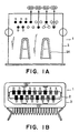
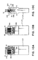
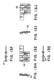
- the connector illustrated in the figures is a receptacle connector 1.
- the receptacle connector 1 comprises a plurality of signal contacts S, a plurality of ground contacts G, a plurality of ordinary (low-speed) contacts D, and an insulator 2 holding the signal contacts S, the ground contacts G, and the ordinary contacts D, and a receptacle shell 3 surrounding all of the above-mentioned components.
- Each pair of the signal contacts S adjacent to each other includes a + signal contact and a - signal contact.
- the contacts of the above-mentioned three types are disposed in a specific arrangement.
- the contacts are arranged in the order of S, S, G, S, S, G, D, D from the right side.
- the contacts are arranged in the order of G, S, S, G, S, S, D, D from the right side.
- the signal contacts S, S adjacent to each other in the upper array and the ground contact G in the lower array are located at three apexes of an isosceles triangle.
- the ground contact G in the upper array and the signal contacts S, S adjacent to each other in the lower array are located at three apexes of an isosceles triangle.
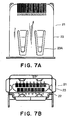
- the receptacle shell 3 has an upper surface provided with a pair of springs 3A.
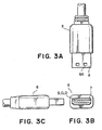
- the springs 3A are adapted to be engaged with a plug connector 6 illustrated in Figs. 3A to 3C.
- the plug connector 6 comprises a plurality of signal contacts S, a plurality of ground contacts G, a plurality of ordinary contacts D, an insulator 7 holding the signal contacts S, the ground contacts G, and the ordinary contacts D, and a plug shell 8 surrounding all of the above-mentioned components.
- the plug shell 8 has an upper surface provided with a pair of holes 8A.
- the holes 8A are adapted to be engaged with the springs 3A of the receptacle connector 1, respectively.
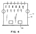
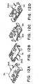
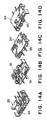
- the connector illustrated in the figures is a receptacle connector 11.
- the receptacle connector 11 comprises a plurality of signal contacts S, a plurality of ground contacts G, a plurality of ordinary contacts D, an insulator 12 holding the signal contacts S, the ground contacts G, and the ordinary contacts D, and a receptacle shell 13 surrounding all of the above-mentioned components.
- the contacts of the above-mentioned three types are disposed in a specific arrangement.
- the contacts are arranged in the order of S, S, S, S, D, D from the right side.
- the contacts are arranged in the order of G, G, G, G, D, D from the right side.
- the contacts are arranged in the order of S, S, S, D from the right side.
- the signal contacts S, S adjacent to each other in the upper array and the ground contact G in the middle array are located at three apexes of an isosceles triangle.
- the ground contact G in the middle array and the signal contacts S, S adjacent to each other in the lower array are located at three apexes of an isosceles triangle.
- the receptacle shell 13 has an upper surface provided with a pair of holes 13A.
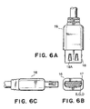
- the holes 13A are adapted to be engaged with a plug connector 16 illustrated in Figs. 6A to 6C.
- the plug connector 16 comprises a plurality of signal contacts S, a plurality of ground contacts G, a plurality or ordinary contacts D, an insulator 17 holding the signal contacts S, the ground contacts G, and the ordinary contacts D, and a plug shell 18 surrounding all of the above-mentioned components.
- the plug shell 18 has an upper surface provided with a pair of springs 18A.
- the springs 18A are adapted to be engaged with the holes 13A of the receptacle connector 11, respectively.
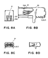
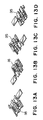
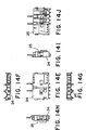
- the connector illustrated in the figures is a receptacle connector 21 of a SMT (Surface Mount) type.
- the receptacle connector 21 comprises a plurality of signal contacts S, a plurality of ground contacts G, a plurality of ordinary contacts D, an insulator 22 holding the signal contacts S, the ground contacts G, and the ordinary contact D, and a receptacle shell 23 surrounding all of the above-mentioned components.
- the contacts of the above-mentioned three types are disposed in a specific arrangement.
- the contacts are arranged in the order of S, S, G, S, S, G, D, D from the right side.
- the contacts are arranged in the order of G, S, S, G, S, S, D, D from the right side.
- the signal contacts S, S adjacent to each other in the upper array and the ground contact G in the lower array are located at three apexes of an isosceles triangle.
- the ground contact G in the upper array and the signal contacts S, S adjacent to each other in the lower array are located at three apexes of an isosceles triangle.
- the contacts are arranged in a single line in the order of S, G, S, S, G, S, S, G, S, S, G, S, D, D, D, D form the right side and exposed from the receptacle shell 23.
- the receptacle shell 23 has an upper surface provided with a pair of springs 23A.
- the springs 23A are adapted to be engaged with a plug connector (not shown).
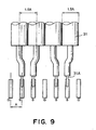
- connection structure of the connector in each embodiment and transmission cables description will be made of a connection structure of the connector in each embodiment and transmission cables.
- each transmission cable 31 has a center conductor 31 A connected to each signal contact S.
- Each of the signal contacts S and the ground contacts G has a terminal portion to be connected to a printed board.
- the terminal portions are arranged in a single line in a manner such that two signal contacts S are arranged adjacent to each other and one ground contact G is arranged next.
- the signal contacts S and the ground contacts G are arranged at a predetermined pitch A.
- a space is left in an area faced to each ground contact G.
- the plug connector with the transmission cables connected thereto is fitted to the receptacle connector mounted to the printed board.
- Each of the signal contacts S, the ground contacts G, and the ordinary contact D may be of a surface-mount type or a through-hole type.
- the transmission cables 31 have shield portions 31 B divided into upper and lower arrays.
- Upper-array and lower-array ground plates 32 and 33 are superposed to each other and inserted between the upper and the lower arrays of the shield portions 31 B.
- the upper-array ground plate 32 has connecting portions 32A connected to the shield portions 31 B of the upper array.
- the lower-array ground plate 33 has connecting portions 33A connected to the shield portions 31 B of the lower array.
- the upper-array and the lower-array ground plates 32 and 33 are provided with lead portions 32B and 33B to be contacted with or soldered to the ground contacts G, respectively.
- the upper-array and the lower-array ground plates 32 and 33 are faced to each other with the lead portions 32B and 33B alternately arranged. In this manner, the lead portions 32B and 33B can be connected to the ground contacts G arranged in a staggered fashion and located at the apexes of the isosceles triangles.
- the lead portions 33B of the lower-array ground plate 33 are connected to the ground contacts G of the upper array while the lead portions 32B of the upper-array ground plate 32 are connected to the ground contacts G of the lower array.
- the lead portions 32B of the upper-array ground plate 32 are connected to the ground contacts G of the upper array while the lead portions 33B of the lower-array ground plate 33 are connected to the ground contacts G of the lower array.
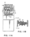
- the shield portion 31 B of each of the transmission cables 31 on both of upper and lower sides may be surrounded by a ground plate 34 on left, right, and lower sides and by a shield plate 35 on an upper side.
- the shield potion 31B of the transmission cable 31 is connected to the ground plate 34 and the shield plate 35.
- the ground plate 34 of the connector is illustrated as seen in different directions.
- the ground plate 34 has one side provided with a pair of lead portions 34A which can be connected to an electric circuit formed on the circuit board.
- the shield plate 35 of the connector is illustrated as seen in different directions.
- the shield plate 35 is engaged with the ground plate 34 to form a combination of the ground plate and the shield plate, as illustrated in Figs. 14A to 14J.
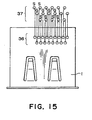
- the contacts 36 are arranged in two rows on the receptacle connector 1. In this condition, the pitch is relatively small or narrow on the receptacle connector 1.
- the contacts 36 may be connected to an electric circuit of the circuit board by inserting the contacts 36 in through holes 37 formed in the circuit board. In this event, the through holes 37 can be arranged in three or more rows. In case where the through holes 37 are arranged in three or more rows, it becomes possible to make the pitch of the through holes 37 be relatively large or widen the pitch on the circuit board. This results in pitch conversion between the contacts 36 and the through holes 37.
Landscapes
- Details Of Connecting Devices For Male And Female Coupling (AREA)
- Coupling Device And Connection With Printed Circuit (AREA)
Claims (4)
- Connecteur comprenant un certain nombre de réseaux de contacts parallèles les uns aux autres, chacun de ces réseaux de contacts comprenant deux contacts de signaux (S) adjacents l'un à l'autre, et un contact de masse (G) aligné avec les contacts de signaux,
caractérisé en ce que
le contact de masse (G) de chaque réseau de contacts est disposé dans une position correspondant à une position intermédiaire entre deux contacts de signaux (S) adjacents l'un à l'autre dans un réseau de contacts suivant. - Connecteur selon la revendication 1,
dans lequel
dans chaque réseau de contacts, le contact de masse (G) est placé de manière à être adjacent à l'un des contacts de signaux (S). - Connecteur selon la revendication 1 ou 2,
dans lequel
les contacts de signaux (S) ont des parties de bornes de signaux, le contact de masse (G) ayant une partie de borne de masse, les parties de bornes de signaux et la partie de borne de masse étant disposées dans un réseau commun unique. - Connecteur selon l'une des revendications 1 à 3,
dans lequel
la partie de borne de masse est disposée entre celles qui sont adjacentes des parties de bornes de signaux.
Applications Claiming Priority (4)
| Application Number | Priority Date | Filing Date | Title |
|---|---|---|---|
| JP2001060862 | 2001-03-05 | ||
| JP2001060862 | 2001-03-05 | ||
| JP2001067706A JP3564555B2 (ja) | 2001-03-05 | 2001-03-09 | 高速ディファレンシャル信号伝送用コネクタ |
| JP2001067706 | 2001-03-09 |
Publications (2)
| Publication Number | Publication Date |
|---|---|
| EP1239552A1 EP1239552A1 (fr) | 2002-09-11 |
| EP1239552B1 true EP1239552B1 (fr) | 2004-06-02 |
Family
ID=26610657
Family Applications (1)
| Application Number | Title | Priority Date | Filing Date |
|---|---|---|---|
| EP02004531A Expired - Lifetime EP1239552B1 (fr) | 2001-03-05 | 2002-02-27 | Connecteur ayant des contacts de signal ou de masse avec une disposition particulière |
Country Status (8)
| Country | Link |
|---|---|
| US (1) | US6935870B2 (fr) |
| EP (1) | EP1239552B1 (fr) |
| JP (1) | JP3564555B2 (fr) |
| KR (1) | KR100461260B1 (fr) |
| CN (1) | CN1269265C (fr) |
| DE (1) | DE60200559T2 (fr) |
| DK (1) | DK1239552T3 (fr) |
| TW (1) | TW580783B (fr) |
Cited By (1)
| Publication number | Priority date | Publication date | Assignee | Title |
|---|---|---|---|---|
| CN101626659B (zh) * | 2004-02-13 | 2011-04-20 | 莫莱克斯公司 | 用于电路板的差分信号电路的高速导孔系统 |
Families Citing this family (71)
| Publication number | Priority date | Publication date | Assignee | Title |
|---|---|---|---|---|
| US6767252B2 (en) * | 2001-10-10 | 2004-07-27 | Molex Incorporated | High speed differential signal edge card connector and circuit board layouts therefor |
| US7039417B2 (en) | 2003-09-25 | 2006-05-02 | Lenovo Pte Ltd | Apparatus, system, and method for mitigating access point data rate degradation |
| WO2004001907A1 (fr) | 2002-06-21 | 2003-12-31 | Molex Incorporated | Connecteur a reglage d'impedance haute densite presentant une structure modulaire |
| EP1459414B1 (fr) * | 2002-09-25 | 2008-12-17 | Molex Incorporated | Agencement de contacts accordes par impedance et connecteurs incorporant cet agencement |
| US6863549B2 (en) | 2002-09-25 | 2005-03-08 | Molex Incorporated | Impedance-tuned terminal contact arrangement and connectors incorporating same |
| JP4082604B2 (ja) | 2003-04-09 | 2008-04-30 | 矢崎総業株式会社 | コネクタ |
| CN100561608C (zh) * | 2003-11-22 | 2009-11-18 | 鸿富锦精密工业(深圳)有限公司 | 消除高速数字电路串扰的差分对排列形式 |
| US7448909B2 (en) | 2004-02-13 | 2008-11-11 | Molex Incorporated | Preferential via exit structures with triad configuration for printed circuit boards |
| EP1841298A3 (fr) * | 2004-02-13 | 2008-05-07 | Molex Incorporated | Structure de sortie pour trous conducteurs de cartes à circuits imprimés |
| JP4036376B2 (ja) * | 2004-04-09 | 2008-01-23 | 日本航空電子工業株式会社 | コネクタ |
| SG117589A1 (en) * | 2004-06-03 | 2005-12-29 | Tyco Electronics Amp Kk | Board mounting electrical connector |
| JP4613043B2 (ja) * | 2004-10-19 | 2011-01-12 | 日本航空電子工業株式会社 | コネクタ |
| EP1810552A1 (fr) | 2004-10-29 | 2007-07-25 | Molex Incorporated | Carte a circuit imprime pour connecteurs electriques a grand debit |
| JP4324566B2 (ja) * | 2005-01-21 | 2009-09-02 | ホシデン株式会社 | メモリカード用アダプタ |
| TWI284950B (en) * | 2005-05-19 | 2007-08-01 | Via Tech Inc | Chip structure with arrangement of side pads |
| CN1905283B (zh) * | 2005-07-29 | 2010-05-26 | 东莞市夏亿电子科技有限公司 | 一种电连接器 |
| JP2007080782A (ja) | 2005-09-16 | 2007-03-29 | Japan Aviation Electronics Industry Ltd | 電気コネクタ |
| KR100827267B1 (ko) | 2005-09-16 | 2008-05-07 | 니혼 고꾸 덴시 고교 가부시끼가이샤 | 누화 억제가 가능한 전기 커넥터 |
| JP4190015B2 (ja) | 2005-11-02 | 2008-12-03 | 日本航空電子工業株式会社 | コネクタ |
| JP4623584B2 (ja) * | 2005-12-28 | 2011-02-02 | 日本航空電子工業株式会社 | コネクタ |
| JP4551868B2 (ja) * | 2005-12-28 | 2010-09-29 | 日本航空電子工業株式会社 | コネクタ |
| JP4216287B2 (ja) | 2006-02-20 | 2009-01-28 | 日本航空電子工業株式会社 | コネクタ |
| CN2932689Y (zh) * | 2006-04-10 | 2007-08-08 | 富士康(昆山)电脑接插件有限公司 | 电连接器 |
| TWI323958B (en) * | 2006-07-14 | 2010-04-21 | Japan Aviation Electron | Electrical component with contact terminal portions arranged in generally trapezoidal shape |
| US7670196B2 (en) | 2006-08-02 | 2010-03-02 | Tyco Electronics Corporation | Electrical terminal having tactile feedback tip and electrical connector for use therewith |
| US7753742B2 (en) | 2006-08-02 | 2010-07-13 | Tyco Electronics Corporation | Electrical terminal having improved insertion characteristics and electrical connector for use therewith |
| US7591655B2 (en) | 2006-08-02 | 2009-09-22 | Tyco Electronics Corporation | Electrical connector having improved electrical characteristics |
| US7549897B2 (en) | 2006-08-02 | 2009-06-23 | Tyco Electronics Corporation | Electrical connector having improved terminal configuration |
| US8142236B2 (en) | 2006-08-02 | 2012-03-27 | Tyco Electronics Corporation | Electrical connector having improved density and routing characteristics and related methods |
| JP5019174B2 (ja) * | 2007-08-03 | 2012-09-05 | 山一電機株式会社 | 高速伝送用コネクタ |
| JP2009037971A (ja) * | 2007-08-03 | 2009-02-19 | Tyco Electronics Amp Kk | 基板実装型コネクタ |
| WO2009025868A1 (fr) * | 2007-08-23 | 2009-02-26 | Molex Incorporated | Connecteur électrique monté sur carte |
| JP4862796B2 (ja) * | 2007-09-28 | 2012-01-25 | 山一電機株式会社 | 高速伝送用高密度コネクタ |
| US7727025B2 (en) * | 2007-10-09 | 2010-06-01 | Tyco Electronics Corporation | Modular electrical connector with enhanced plug interface |
| CN201122731Y (zh) * | 2007-10-25 | 2008-09-24 | 上海莫仕连接器有限公司 | 电连接器 |
| JP4548802B2 (ja) * | 2008-01-29 | 2010-09-22 | 日本航空電子工業株式会社 | コネクタ |
| JP4522454B2 (ja) * | 2008-02-04 | 2010-08-11 | 日本航空電子工業株式会社 | コネクタ |
| JP2009193786A (ja) * | 2008-02-13 | 2009-08-27 | Yamaichi Electronics Co Ltd | Hdmi規格ケーブル用コネクタ |
| JP4459273B2 (ja) * | 2008-02-20 | 2010-04-28 | 日本航空電子工業株式会社 | コネクタ |
| JP4671444B2 (ja) * | 2008-02-20 | 2011-04-20 | 日本航空電子工業株式会社 | コネクタ |
| US8506332B2 (en) * | 2008-02-26 | 2013-08-13 | Molex Incorporated | Impedance controlled electrical connector |
| JP5100449B2 (ja) * | 2008-03-05 | 2012-12-19 | キヤノン株式会社 | 複合コネクタおよびそれを備える電子機器 |
| US7748997B2 (en) * | 2008-07-22 | 2010-07-06 | Tyco Electronics Corporation | Receptacle for electrical connectors |
| JP4567079B2 (ja) * | 2008-08-22 | 2010-10-20 | 日本航空電子工業株式会社 | コネクタ |
| JP4565031B2 (ja) * | 2008-09-17 | 2010-10-20 | 山一電機株式会社 | 高速伝送用コネクタ、高速伝送コネクタ用プラグ、および、高速伝送コネクタ用ソケット |
| US7972151B2 (en) * | 2009-01-05 | 2011-07-05 | Hon Hai Precision Ind. Co., Ltd. | Electrical connector with improved arrangement of ground and signal contacts |
| US8066532B2 (en) * | 2009-01-18 | 2011-11-29 | Hon Hai Precision Ind. Co., Ltd. | Electrical connector assembly with improved contact arrangement and metallic shell |
| JP2010244901A (ja) * | 2009-04-07 | 2010-10-28 | Japan Aviation Electronics Industry Ltd | コネクタ |
| US8932081B2 (en) | 2009-07-01 | 2015-01-13 | Molex Incorporated | Connector with terminal retention |
| TWI376842B (en) * | 2009-09-18 | 2012-11-11 | Via Tech Inc | Lead arrangement, electric connector and electric assembly |
| US8740651B2 (en) | 2009-09-18 | 2014-06-03 | Via Technologies, Inc. | Lead arrangement, electric connector and electric assembly |
| JP4828626B2 (ja) * | 2009-10-20 | 2011-11-30 | 日本航空電子工業株式会社 | コネクタ |
| DE102009057260A1 (de) | 2009-12-08 | 2011-08-04 | ERNI Electronics GmbH, 73099 | Relief-Steckverbinder und Multilayerplatine |
| CN102117978B (zh) * | 2009-12-30 | 2014-07-30 | 富士康(昆山)电脑接插件有限公司 | 电连接器 |
| CN102315534B (zh) * | 2010-07-08 | 2014-08-20 | 泰科电子(上海)有限公司 | 电连接器 |
| JP4976568B1 (ja) * | 2011-04-18 | 2012-07-18 | 日本航空電子工業株式会社 | コネクタ |
| MY167297A (en) * | 2011-08-05 | 2018-08-16 | Molex Interconnect Shanghai Co | Electrical connector with power terminals |
| CN102916281B (zh) * | 2011-08-05 | 2015-04-01 | 上海莫仕连接器有限公司 | 插头电连接器、插座电连接器及电连接器组合 |
| JP5727902B2 (ja) * | 2011-09-13 | 2015-06-03 | ホシデン株式会社 | コネクタ |
| CN103094736B (zh) * | 2011-11-07 | 2015-07-08 | 富士康(昆山)电脑接插件有限公司 | 线缆连接器组件 |
| CN202772376U (zh) * | 2012-08-29 | 2013-03-06 | 泰科电子(上海)有限公司 | 连接器 |
| CN105765797B (zh) | 2013-11-27 | 2019-07-05 | 安费诺富加宜(亚洲)私人有限公司 | 电力连接器 |
| TWI581517B (zh) * | 2014-07-14 | 2017-05-01 | 連展科技股份有限公司 | Socket electrical connector |
| US9338879B2 (en) * | 2014-07-17 | 2016-05-10 | Via Technologies, Inc. | Through-hole layout structure including first and second pairs of differential signal through-holes disposed between three ground through-holes |
| JP6330587B2 (ja) * | 2014-09-04 | 2018-05-30 | 株式会社オートネットワーク技術研究所 | 通信用コネクタ |
| US9496651B2 (en) * | 2015-03-03 | 2016-11-15 | Lattice Semiconductor Corporation | HDMI connector |
| CN204966770U (zh) * | 2015-07-25 | 2016-01-13 | 富士康(昆山)电脑接插件有限公司 | 电连接器 |
| CN108141677B (zh) * | 2015-10-26 | 2020-02-14 | 华为技术有限公司 | 一种扬声器模组、音频补偿方法和装置 |
| CN107978926B (zh) * | 2016-10-21 | 2020-06-30 | 泰科电子(上海)有限公司 | 连接器 |
| CN107221820B (zh) * | 2017-06-29 | 2024-02-27 | 深圳市深台帏翔电子有限公司 | 终端设备及其集成连接器 |
| CN109586067B (zh) * | 2018-10-23 | 2020-06-09 | 番禺得意精密电子工业有限公司 | 电连接器 |
Citations (1)
| Publication number | Priority date | Publication date | Assignee | Title |
|---|---|---|---|---|
| US5525067A (en) * | 1994-02-03 | 1996-06-11 | Motorola, Inc | Ground plane interconnection system using multiple connector contacts |
Family Cites Families (18)
| Publication number | Priority date | Publication date | Assignee | Title |
|---|---|---|---|---|
| JPH03110772A (ja) | 1989-09-22 | 1991-05-10 | Tanaka Kikinzoku Kogyo Kk | 多線束摺動ブラシ素材の製造方法 |
| JP2587316B2 (ja) * | 1990-10-08 | 1997-03-05 | 第一電子工業株式会社 | 同軸フラットケーブル用多極電気コネクタ |
| JP2739608B2 (ja) * | 1990-11-15 | 1998-04-15 | 日本エー・エム・ピー株式会社 | 信号伝送用マルチコンタクト型コネクタ |
| JPH04269479A (ja) | 1991-02-25 | 1992-09-25 | Fujitsu Ltd | 高密度コネクタ |
| JP3415889B2 (ja) | 1992-08-18 | 2003-06-09 | ザ ウィタカー コーポレーション | シールドコネクタ |
| JPH06104030A (ja) * | 1992-09-18 | 1994-04-15 | Mitsubishi Electric Corp | コネクタ |
| US5716236A (en) * | 1996-03-01 | 1998-02-10 | Molex Incorporated | System for terminating the shield of a high speed cable |
| US5711686A (en) | 1996-03-01 | 1998-01-27 | Molex Incorporated | System for terminating the shield of a high speed cable |
| US5895276A (en) * | 1996-11-22 | 1999-04-20 | The Whitaker Corporation | High speed and high density backplane connector |
| US5876248A (en) * | 1997-01-14 | 1999-03-02 | Molex Incorporated | Matable electrical connectors having signal and power terminals |
| JPH1167369A (ja) * | 1997-08-18 | 1999-03-09 | Japan Aviation Electron Ind Ltd | 高速伝送に適したコネクタ |
| US5961355A (en) | 1997-12-17 | 1999-10-05 | Berg Technology, Inc. | High density interstitial connector system |
| JP3236994B2 (ja) | 1998-02-27 | 2001-12-10 | 日本航空電子工業株式会社 | コネクタ |
| JPH11251003A (ja) * | 1998-02-27 | 1999-09-17 | Yokowo Co Ltd | Zifコネクタ |
| US6280209B1 (en) * | 1999-07-16 | 2001-08-28 | Molex Incorporated | Connector with improved performance characteristics |
| DE60014385T2 (de) * | 1999-07-16 | 2006-02-23 | Molex Inc., Lisle | Impedanz-abgestimmter verbinder |
| JP3678990B2 (ja) | 2000-03-31 | 2005-08-03 | タイコエレクトロニクスアンプ株式会社 | 電気コネクタ組立体および雌コネクタ |
| US6350134B1 (en) * | 2000-07-25 | 2002-02-26 | Tyco Electronics Corporation | Electrical connector having triad contact groups arranged in an alternating inverted sequence |
-
2001
- 2001-03-09 JP JP2001067706A patent/JP3564555B2/ja not_active Expired - Lifetime
-
2002
- 2002-02-27 EP EP02004531A patent/EP1239552B1/fr not_active Expired - Lifetime
- 2002-02-27 DK DK02004531T patent/DK1239552T3/da active
- 2002-02-27 DE DE60200559T patent/DE60200559T2/de not_active Expired - Fee Related
- 2002-03-01 TW TW091103808A patent/TW580783B/zh not_active IP Right Cessation
- 2002-03-05 CN CNB021067406A patent/CN1269265C/zh not_active Expired - Lifetime
- 2002-03-05 US US10/090,956 patent/US6935870B2/en not_active Expired - Lifetime
- 2002-03-05 KR KR10-2002-0011613A patent/KR100461260B1/ko not_active Expired - Lifetime
Patent Citations (1)
| Publication number | Priority date | Publication date | Assignee | Title |
|---|---|---|---|---|
| US5525067A (en) * | 1994-02-03 | 1996-06-11 | Motorola, Inc | Ground plane interconnection system using multiple connector contacts |
Cited By (1)
| Publication number | Priority date | Publication date | Assignee | Title |
|---|---|---|---|---|
| CN101626659B (zh) * | 2004-02-13 | 2011-04-20 | 莫莱克斯公司 | 用于电路板的差分信号电路的高速导孔系统 |
Also Published As
| Publication number | Publication date |
|---|---|
| DE60200559D1 (de) | 2004-07-08 |
| CN1269265C (zh) | 2006-08-09 |
| JP2002334748A (ja) | 2002-11-22 |
| US20020123254A1 (en) | 2002-09-05 |
| KR100461260B1 (ko) | 2004-12-10 |
| KR20020071477A (ko) | 2002-09-12 |
| US6935870B2 (en) | 2005-08-30 |
| DE60200559T2 (de) | 2005-06-30 |
| DK1239552T3 (da) | 2004-10-04 |
| TW580783B (en) | 2004-03-21 |
| CN1374719A (zh) | 2002-10-16 |
| JP3564555B2 (ja) | 2004-09-15 |
| EP1239552A1 (fr) | 2002-09-11 |
Similar Documents
| Publication | Publication Date | Title |
|---|---|---|
| EP1239552B1 (fr) | Connecteur ayant des contacts de signal ou de masse avec une disposition particulière | |
| US7128611B2 (en) | Electric connector including signal contact pairs and ground contacts provided in rows at a first end, in which the ground contacts are provided between signal contact pairs from the respective rows at a second end | |
| US8157573B2 (en) | Connector | |
| US6336827B1 (en) | Balanced-transmission cable-and-connector unit | |
| CN100511870C (zh) | 可保持接地接点与一对信号接点之间物理距离平衡的连接器 | |
| US7497704B2 (en) | Electrical connector capable of suppressing crosstalk | |
| US6524119B2 (en) | Connector adapted to handling of different kinds of signals including high-speed signals | |
| US7604490B2 (en) | Electrical connector with improved ground piece | |
| KR101571607B1 (ko) | 커넥터 및 이를 이용한 신호 전송 방법 | |
| JP4542579B2 (ja) | コネクタ | |
| US20020048995A1 (en) | High-speed transmission connector with a ground structure having an improved shielding function | |
| US6176743B1 (en) | Electrical adapter | |
| US10653000B2 (en) | Electrical connector assembly capable of transmitting high-frequency signals | |
| US7462059B2 (en) | Connector | |
| EP0907219B1 (fr) | Embase de connexion coaxiale faite à partir de tôle poinçonnée | |
| US6783400B2 (en) | Electrical connector assembly having contacts configured for high-speed signal transmission | |
| KR20120112497A (ko) | 기판실장 커넥터 | |
| KR100603862B1 (ko) | 전기 커넥터 및 전송 라인 | |
| US6953367B2 (en) | Electrical connector | |
| US6261106B1 (en) | IC card connector apparatus | |
| JP4843263B2 (ja) | フレキシブルプリントケーブル用コネクタ | |
| JP2012174597A (ja) | 差動信号用コネクタ | |
| US6340314B1 (en) | Electrical adapter |
Legal Events
| Date | Code | Title | Description |
|---|---|---|---|
| PUAI | Public reference made under article 153(3) epc to a published international application that has entered the european phase |
Free format text: ORIGINAL CODE: 0009012 |
|
| AK | Designated contracting states |
Kind code of ref document: A1 Designated state(s): AT BE CH CY DE DK ES FI FR GB GR IE IT LI LU MC NL PT SE TR |
|
| AX | Request for extension of the european patent |
Free format text: AL;LT;LV;MK;RO;SI |
|
| 17P | Request for examination filed |
Effective date: 20030311 |
|
| AKX | Designation fees paid |
Designated state(s): DE DK FI FR GB SE |
|
| 17Q | First examination report despatched |
Effective date: 20030417 |
|
| GRAP | Despatch of communication of intention to grant a patent |
Free format text: ORIGINAL CODE: EPIDOSNIGR1 |
|
| GRAA | (expected) grant |
Free format text: ORIGINAL CODE: 0009210 |
|
| GRAS | Grant fee paid |
Free format text: ORIGINAL CODE: EPIDOSNIGR3 |
|
| AK | Designated contracting states |
Kind code of ref document: B1 Designated state(s): DE DK FI FR GB SE |
|
| REG | Reference to a national code |
Ref country code: GB Ref legal event code: FG4D |
|
| REF | Corresponds to: |
Ref document number: 60200559 Country of ref document: DE Date of ref document: 20040708 Kind code of ref document: P |
|
| REG | Reference to a national code |
Ref country code: IE Ref legal event code: FG4D |
|
| REG | Reference to a national code |
Ref country code: SE Ref legal event code: TRGR |
|
| REG | Reference to a national code |
Ref country code: DK Ref legal event code: T3 |
|
| ET | Fr: translation filed | ||
| PLBE | No opposition filed within time limit |
Free format text: ORIGINAL CODE: 0009261 |
|
| STAA | Information on the status of an ep patent application or granted ep patent |
Free format text: STATUS: NO OPPOSITION FILED WITHIN TIME LIMIT |
|
| 26N | No opposition filed |
Effective date: 20050303 |
|
| PGFP | Annual fee paid to national office [announced via postgrant information from national office to epo] |
Ref country code: DK Payment date: 20080130 Year of fee payment: 7 |
|
| PGFP | Annual fee paid to national office [announced via postgrant information from national office to epo] |
Ref country code: DE Payment date: 20080229 Year of fee payment: 7 Ref country code: FI Payment date: 20080204 Year of fee payment: 7 Ref country code: GB Payment date: 20080129 Year of fee payment: 7 Ref country code: SE Payment date: 20080213 Year of fee payment: 7 |
|
| PGFP | Annual fee paid to national office [announced via postgrant information from national office to epo] |
Ref country code: FR Payment date: 20080228 Year of fee payment: 7 |
|
| EUG | Se: european patent has lapsed | ||
| REG | Reference to a national code |
Ref country code: DK Ref legal event code: EBP |
|
| GBPC | Gb: european patent ceased through non-payment of renewal fee |
Effective date: 20090227 |
|
| PG25 | Lapsed in a contracting state [announced via postgrant information from national office to epo] |
Ref country code: FI Free format text: LAPSE BECAUSE OF NON-PAYMENT OF DUE FEES Effective date: 20090227 |
|
| REG | Reference to a national code |
Ref country code: FR Ref legal event code: ST Effective date: 20091030 |
|
| PG25 | Lapsed in a contracting state [announced via postgrant information from national office to epo] |
Ref country code: DE Free format text: LAPSE BECAUSE OF NON-PAYMENT OF DUE FEES Effective date: 20090901 |
|
| PG25 | Lapsed in a contracting state [announced via postgrant information from national office to epo] |
Ref country code: GB Free format text: LAPSE BECAUSE OF NON-PAYMENT OF DUE FEES Effective date: 20090227 Ref country code: FR Free format text: LAPSE BECAUSE OF NON-PAYMENT OF DUE FEES Effective date: 20090302 |
|
| PG25 | Lapsed in a contracting state [announced via postgrant information from national office to epo] |
Ref country code: DK Free format text: LAPSE BECAUSE OF NON-PAYMENT OF DUE FEES Effective date: 20090831 |
|
| PG25 | Lapsed in a contracting state [announced via postgrant information from national office to epo] |
Ref country code: SE Free format text: LAPSE BECAUSE OF NON-PAYMENT OF DUE FEES Effective date: 20090228 |