EP1237185A2 - Verfahren zur Herstellung isolierender Strukturen - Google Patents
Verfahren zur Herstellung isolierender Strukturen Download PDFInfo
- Publication number
- EP1237185A2 EP1237185A2 EP02003714A EP02003714A EP1237185A2 EP 1237185 A2 EP1237185 A2 EP 1237185A2 EP 02003714 A EP02003714 A EP 02003714A EP 02003714 A EP02003714 A EP 02003714A EP 1237185 A2 EP1237185 A2 EP 1237185A2
- Authority
- EP
- European Patent Office
- Prior art keywords
- layer
- silicon carbide
- carbide layer
- oxide layer
- isolating structures
- Prior art date
- Legal status (The legal status is an assumption and is not a legal conclusion. Google has not performed a legal analysis and makes no representation as to the accuracy of the status listed.)
- Withdrawn
Links
Images


Classifications
-
- H—ELECTRICITY
- H10—SEMICONDUCTOR DEVICES; ELECTRIC SOLID-STATE DEVICES NOT OTHERWISE PROVIDED FOR
- H10W—GENERIC PACKAGES, INTERCONNECTIONS, CONNECTORS OR OTHER CONSTRUCTIONAL DETAILS OF DEVICES COVERED BY CLASS H10
- H10W10/00—Isolation regions in semiconductor bodies between components of integrated devices
- H10W10/01—Manufacture or treatment
- H10W10/011—Manufacture or treatment of isolation regions comprising dielectric materials
- H10W10/014—Manufacture or treatment of isolation regions comprising dielectric materials using trench refilling with dielectric materials, e.g. shallow trench isolations
-
- H—ELECTRICITY
- H10—SEMICONDUCTOR DEVICES; ELECTRIC SOLID-STATE DEVICES NOT OTHERWISE PROVIDED FOR
- H10W—GENERIC PACKAGES, INTERCONNECTIONS, CONNECTORS OR OTHER CONSTRUCTIONAL DETAILS OF DEVICES COVERED BY CLASS H10
- H10W10/00—Isolation regions in semiconductor bodies between components of integrated devices
- H10W10/01—Manufacture or treatment
-
- H—ELECTRICITY
- H10—SEMICONDUCTOR DEVICES; ELECTRIC SOLID-STATE DEVICES NOT OTHERWISE PROVIDED FOR
- H10W—GENERIC PACKAGES, INTERCONNECTIONS, CONNECTORS OR OTHER CONSTRUCTIONAL DETAILS OF DEVICES COVERED BY CLASS H10
- H10W10/00—Isolation regions in semiconductor bodies between components of integrated devices
- H10W10/10—Isolation regions comprising dielectric materials
- H10W10/17—Isolation regions comprising dielectric materials formed using trench refilling with dielectric materials, e.g. shallow trench isolations
Definitions
- the present invention relates to a method for manufacturing isolating structures, in particular in a substrate of silicon carbide.
- the invention relates to a method for manufacturing isolating structures in a silicon carbide layer, which method comprises the following steps:
- the invention further relates to an isolating structure.
- the invention relates, particularly but not exclusively, to a method for manufacturing isolating structures in silicon carbide layers, and reference will be made throughout this description to this field of application for convenience of illustration.
- silicon carbide is an extremely resistant material to chemical etching. Removing a portion of silicon carbide by ordinary etching techniques as employed in standard silicon-integrated circuits manufacturing processes proves difficult.
- a first prior method for etching away such layers is based on the use of a fluorine solution utilizing a specially dense plasma.
- the underlying technical problem of this invention is to provide a method for manufacturing isolating structures in silicon carbide layers, which be compatible with standard microelectronic device manufacturing techniques and is effective to overcome the limitations with which prior methods are beset.
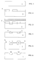
- a masking layer 2 of a photoresist or metal e.g. silicon oxide, is formed over the surface of a substrate 1 of silicon carbide (SiC).
- Openings 2a are formed through the masking layer 2, using conventional photolithographic techniques and successive etching steps, so as to expose the substrate portions where the isolating regions (trenches) 3a are to be formed.
- an ion implanting step is carried out to implant the chip surface with heavy ions or dopant throughout.
- the ion implanting step will result in the substrate 1 becoming "damaged", in the sense that its Si-C lattice structure undergoes alteration.
- the depth of the "damaged" regions 3 can be varied by changing parameters, such as energy and dosage, of the implanting step.
- the whole substrate 1 is subjected to an oxidizing step.
- An oxide layer 4 is formed over the chip surface. As is known, during the heat treating process, a surface portion of the substrate 1 is also converted into the oxide layer 4.
- the oxide layer 4 has a first portion 5 with a first thickness in the regions 3, while on the rest of the substrate 1, the oxide layer 4 has a second portion 6 with a second thickness smaller than the first thickness.
- the difference is due to variations in the lattice structure of the implanted regions 3, generated during the ion implanting step, causing the rate of oxidation of the silicon carbide layer to increase, and consequently, the oxide layer 4 to grow thicker.
- FIG. 21 shows a plot of the thickness of the oxide grown over SiC against time at different oxidation temperatures.
- the rate of oxidation increases substantially as ions are implanted in the SiC substrate 1.
- the thickness of the oxide layer in the regions 3 is 2.5 ⁇ m, against an oxide layer 500 nm thick in the undamaged portion.
- the depth of the oxide layer in the substrate would be 1 ⁇ m, when a conventional 1% fluorine technique is used.
- a step of removing the oxide layer from both the surface of the substrate 1 and the regions 3 results in isolating regions (trenches) 3A being defined depthwise in the substrate 1.
- the isolating regions and their trenches are formed by etching through the layer of silicon oxide rather than the silicon carbide.
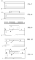
- the method of this invention is specially advantageous where isolating trenches are to be formed for an epitaxially grown diode.
- a first epitaxial layer 7 doped with impurities of the N type at a relatively low dopant concentration, and a second epitaxial layer 8 doped with P-type impurities at a relatively high dopant concentration, are formed over the surface of a silicon carbide substrate 1.
- the second layer 8 is thinner than the first layer 7.
- a masking layer 2 of a photoresist or metal or silicon oxide is formed over the second epitaxial layer 8.
- the masking layer 2 is partially etched away to expose substrate portions where the isolating regions 3 will be formed.
- the whole chip surface is ion implanted.
- heavy ions are implanted in the substrate portion where isolation is to be provided.
- the structure of the layer 8 becomes "damaged" in the regions 3.
- the whole substrate 1 is subjected to an oxidizing step.
- an oxide layer 4 is formed, which has a first portion 5 with a first thickness in the regions 3, while in the epitaxial layer 8, it has a second portion 6 with a second thickness that is smaller than the first thickness.
- the depth of the first portion of the oxide layer 4 will be greater than the depth of the second epitaxial layer 8. Consequently, the second layer 8 is surface isolated from the edge of the structure and forms the anode of the diode.
- the oxide layer 4 can be removed completely and a suitable insulative material substituted for it.
- An opening 4a is then formed through the oxide layer 4 such that at least a portion of the layer 8 can be exposed.
- the diode manufacturing process is then completed by forming conventional metal layers 10.
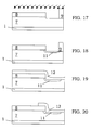
- the method of this invention can also be applied to forming edge structures.
- a method of making an isolating structure for a diode formed as above will now be discussed with reference to Figures 7 to 13.
- the oxide layer 4 is removed completely to form a trench 4A.
- a mask 9 known as a ring mask, is formed on the chip edge, this being followed by an implanting step that affects the whole chip.
- this implantation is provided at an inclination angle effective to produce an implanted region 11 that extends across the bottom and the sidewalls of the trench 4A.
- the invention comprises carrying out an oxidation process all over the chip, in order to form an oxide layer 12 for diode edge isolation.
- isolating structures or trenches can be formed in the layers of silicon carbide by standard integrated circuit manufacturing techniques.
- the inventive method effectively improves the rate of oxidation of the silicon carbide layer.
- the process of removing the oxidized carbide layer is quite compatible with standard removal techniques for integrated circuits, making for faster and more efficient removal operations.
Landscapes
- Element Separation (AREA)
- Formation Of Insulating Films (AREA)
- Drying Of Semiconductors (AREA)
- Processing Of Terminals (AREA)
Applications Claiming Priority (2)
| Application Number | Priority Date | Filing Date | Title |
|---|---|---|---|
| IT2001MI000339A ITMI20010339A1 (it) | 2001-02-20 | 2001-02-20 | Metodo per realizzare strutture isolanti |
| ITMI010339 | 2001-02-20 |
Publications (2)
| Publication Number | Publication Date |
|---|---|
| EP1237185A2 true EP1237185A2 (de) | 2002-09-04 |
| EP1237185A3 EP1237185A3 (de) | 2003-07-30 |
Family
ID=11446939
Family Applications (1)
| Application Number | Title | Priority Date | Filing Date |
|---|---|---|---|
| EP02003714A Withdrawn EP1237185A3 (de) | 2001-02-20 | 2002-02-19 | Verfahren zur Herstellung isolierender Strukturen |
Country Status (3)
| Country | Link |
|---|---|
| US (1) | US6762112B2 (de) |
| EP (1) | EP1237185A3 (de) |
| IT (1) | ITMI20010339A1 (de) |
Cited By (2)
| Publication number | Priority date | Publication date | Assignee | Title |
|---|---|---|---|---|
| FR2888665A1 (fr) * | 2005-07-18 | 2007-01-19 | St Microelectronics Crolles 2 | Procede de realisation d'un transistor mos et circuit integre correspondant |
| CN110943369A (zh) * | 2018-09-21 | 2020-03-31 | 阿尔戈人工智能有限责任公司 | 单片串联连接的激光器二极管阵列及其形成方法 |
Families Citing this family (6)
| Publication number | Priority date | Publication date | Assignee | Title |
|---|---|---|---|---|
| US7808029B2 (en) * | 2006-04-26 | 2010-10-05 | Siliconix Technology C.V. | Mask structure for manufacture of trench type semiconductor device |
| US8084811B2 (en) * | 2009-10-08 | 2011-12-27 | Monolithic Power Systems, Inc. | Power devices with super junctions and associated methods manufacturing |
| US20150050358A1 (en) * | 2013-08-15 | 2015-02-19 | Regents Of The University Of Minnesota | Implant support composition and methods of use |
| EP3800660B1 (de) | 2019-10-02 | 2025-02-19 | STMicroelectronics S.r.l. | Siliciumcarbid-leistungsvorrichtung mit verbesserter robustheit und entsprechendes herstellungsverfahren |
| CN216413051U (zh) | 2020-09-04 | 2022-04-29 | 意法半导体股份有限公司 | 半导体设备 |
| JP7758501B2 (ja) | 2020-09-04 | 2025-10-22 | エスティーマイクロエレクトロニクス エス.アール.エル. | 信頼性を改善した電子装置の要素の製造方法、及び関連要素、電子装置、及び電子機器 |
Family Cites Families (3)
| Publication number | Priority date | Publication date | Assignee | Title |
|---|---|---|---|---|
| JP2670563B2 (ja) * | 1988-10-12 | 1997-10-29 | 富士通株式会社 | 半導体装置の製造方法 |
| US5270244A (en) * | 1993-01-25 | 1993-12-14 | North Carolina State University At Raleigh | Method for forming an oxide-filled trench in silicon carbide |
| KR100312568B1 (ko) * | 1996-04-18 | 2003-06-19 | 마쯔시다덴기산교 가부시키가이샤 | Sic 소자 및 그 제조방법 |
-
2001
- 2001-02-20 IT IT2001MI000339A patent/ITMI20010339A1/it unknown
-
2002
- 2002-02-19 EP EP02003714A patent/EP1237185A3/de not_active Withdrawn
- 2002-02-20 US US10/079,925 patent/US6762112B2/en not_active Expired - Lifetime
Cited By (4)
| Publication number | Priority date | Publication date | Assignee | Title |
|---|---|---|---|---|
| FR2888665A1 (fr) * | 2005-07-18 | 2007-01-19 | St Microelectronics Crolles 2 | Procede de realisation d'un transistor mos et circuit integre correspondant |
| EP1746643A1 (de) * | 2005-07-18 | 2007-01-24 | STMicroelectronics (Crolles 2) SAS | Herstellungsverfahren eines MOS-Transistors und entsprechende integrierte Schaltung. |
| US7749858B2 (en) | 2005-07-18 | 2010-07-06 | Stmicroelectronics (Crolles 2) Sas | Process for producing an MOS transistor and corresponding integrated circuit |
| CN110943369A (zh) * | 2018-09-21 | 2020-03-31 | 阿尔戈人工智能有限责任公司 | 单片串联连接的激光器二极管阵列及其形成方法 |
Also Published As
| Publication number | Publication date |
|---|---|
| US20030003680A1 (en) | 2003-01-02 |
| EP1237185A3 (de) | 2003-07-30 |
| ITMI20010339A1 (it) | 2002-08-20 |
| US6762112B2 (en) | 2004-07-13 |
Similar Documents
| Publication | Publication Date | Title |
|---|---|---|
| CA1216075A (en) | Wafer fabrication by implanting through protective layer | |
| US7285433B2 (en) | Integrated devices with optical and electrical isolation and method for making | |
| CA2672259A1 (en) | Method of manufacturing semiconductor device | |
| EP0564191A2 (de) | Struktur und Verfahren zur Herstellung von integrierten Schaltungen | |
| EP1000439B1 (de) | Verfahren zur herstellung von seitlich dielektrisch isolierten halbleiterbauelementen | |
| US5733813A (en) | Method for forming planarized field isolation regions | |
| US6762112B2 (en) | Method for manufacturing isolating structures | |
| US5476800A (en) | Method for formation of a buried layer for a semiconductor device | |
| JP3407023B2 (ja) | 半導体装置の製造方法 | |
| US7192840B2 (en) | Semiconductor device fabrication method using oxygen ion implantation | |
| CN113838745A (zh) | 用于制造沟槽mosfet的方法 | |
| US4635344A (en) | Method of low encroachment oxide isolation of a semiconductor device | |
| JPH03152954A (ja) | 集積misfetデバイス中に電界分離構造及びゲート構造を形成する方法 | |
| EP0293979A2 (de) | Oxydisolierungsstruktur ohne bird-beak für integrierte Schaltungen | |
| US5763316A (en) | Substrate isolation process to minimize junction leakage | |
| JPH05102297A (ja) | 半導体装置の製造方法 | |
| JP2003197734A (ja) | 半導体装置の素子分離膜の形成方法 | |
| TWI578403B (zh) | 溝渠式蕭基二極體及其製作方法 | |
| US20090170276A1 (en) | Method of Forming Trench of Semiconductor Device | |
| KR100290901B1 (ko) | 반도체소자의격리막형성방법 | |
| KR0161727B1 (ko) | 반도체 소자의 소자분리방법 | |
| EP0462416A2 (de) | Verfahren zum Herstellen von N- und P-Wannen in einem Siliciumsubstrat mittels einer allgemeinen P-Wannenimplantation und ohne N-Wannendampfoxydationsstufe | |
| KR100359162B1 (ko) | 트랜지스터의 제조 방법 | |
| KR100335122B1 (ko) | 반도체 소자의 격리 방법 | |
| KR100373710B1 (ko) | 반도체 소자의 얕은 트렌치 소자 분리 영역 형성 방법 |
Legal Events
| Date | Code | Title | Description |
|---|---|---|---|
| PUAI | Public reference made under article 153(3) epc to a published international application that has entered the european phase |
Free format text: ORIGINAL CODE: 0009012 |
|
| AK | Designated contracting states |
Kind code of ref document: A2 Designated state(s): AT BE CH CY DE DK ES FI FR GB GR IE IT LI LU MC NL PT SE TR |
|
| AX | Request for extension of the european patent |
Free format text: AL;LT;LV;MK;RO;SI |
|
| PUAL | Search report despatched |
Free format text: ORIGINAL CODE: 0009013 |
|
| AK | Designated contracting states |
Designated state(s): AT BE CH CY DE DK ES FI FR GB GR IE IT LI LU MC NL PT SE TR |
|
| AX | Request for extension of the european patent |
Extension state: AL LT LV MK RO SI |
|
| 17P | Request for examination filed |
Effective date: 20040112 |
|
| AKX | Designation fees paid |
Designated state(s): DE FR GB IT |
|
| 17Q | First examination report despatched |
Effective date: 20041019 |
|
| STAA | Information on the status of an ep patent application or granted ep patent |
Free format text: STATUS: THE APPLICATION IS DEEMED TO BE WITHDRAWN |
|
| 18D | Application deemed to be withdrawn |
Effective date: 20050728 |