EP1237139B1 - Anzeigevorrichtung und ansteuerverfahren dafür - Google Patents
Anzeigevorrichtung und ansteuerverfahren dafür Download PDFInfo
- Publication number
- EP1237139B1 EP1237139B1 EP01922019.3A EP01922019A EP1237139B1 EP 1237139 B1 EP1237139 B1 EP 1237139B1 EP 01922019 A EP01922019 A EP 01922019A EP 1237139 B1 EP1237139 B1 EP 1237139B1
- Authority
- EP
- European Patent Office
- Prior art keywords
- voltage
- electrode
- pixel
- capacitance
- display apparatus
- Prior art date
- Legal status (The legal status is an assumption and is not a legal conclusion. Google has not performed a legal analysis and makes no representation as to the accuracy of the status listed.)
- Expired - Lifetime
Links
Images


Classifications
-
- G—PHYSICS
- G09—EDUCATION; CRYPTOGRAPHY; DISPLAY; ADVERTISING; SEALS
- G09G—ARRANGEMENTS OR CIRCUITS FOR CONTROL OF INDICATING DEVICES USING STATIC MEANS TO PRESENT VARIABLE INFORMATION
- G09G3/00—Control arrangements or circuits, of interest only in connection with visual indicators other than cathode-ray tubes
- G09G3/20—Control arrangements or circuits, of interest only in connection with visual indicators other than cathode-ray tubes for presentation of an assembly of a number of characters, e.g. a page, by composing the assembly by combination of individual elements arranged in a matrix no fixed position being assigned to or needed to be assigned to the individual characters or partial characters
- G09G3/22—Control arrangements or circuits, of interest only in connection with visual indicators other than cathode-ray tubes for presentation of an assembly of a number of characters, e.g. a page, by composing the assembly by combination of individual elements arranged in a matrix no fixed position being assigned to or needed to be assigned to the individual characters or partial characters using controlled light sources
- G09G3/30—Control arrangements or circuits, of interest only in connection with visual indicators other than cathode-ray tubes for presentation of an assembly of a number of characters, e.g. a page, by composing the assembly by combination of individual elements arranged in a matrix no fixed position being assigned to or needed to be assigned to the individual characters or partial characters using controlled light sources using electroluminescent panels
- G09G3/32—Control arrangements or circuits, of interest only in connection with visual indicators other than cathode-ray tubes for presentation of an assembly of a number of characters, e.g. a page, by composing the assembly by combination of individual elements arranged in a matrix no fixed position being assigned to or needed to be assigned to the individual characters or partial characters using controlled light sources using electroluminescent panels semiconductive, e.g. using light-emitting diodes [LED]
- G09G3/3208—Control arrangements or circuits, of interest only in connection with visual indicators other than cathode-ray tubes for presentation of an assembly of a number of characters, e.g. a page, by composing the assembly by combination of individual elements arranged in a matrix no fixed position being assigned to or needed to be assigned to the individual characters or partial characters using controlled light sources using electroluminescent panels semiconductive, e.g. using light-emitting diodes [LED] organic, e.g. using organic light-emitting diodes [OLED]
- G09G3/3225—Control arrangements or circuits, of interest only in connection with visual indicators other than cathode-ray tubes for presentation of an assembly of a number of characters, e.g. a page, by composing the assembly by combination of individual elements arranged in a matrix no fixed position being assigned to or needed to be assigned to the individual characters or partial characters using controlled light sources using electroluminescent panels semiconductive, e.g. using light-emitting diodes [LED] organic, e.g. using organic light-emitting diodes [OLED] using an active matrix
-
- G—PHYSICS
- G09—EDUCATION; CRYPTOGRAPHY; DISPLAY; ADVERTISING; SEALS
- G09G—ARRANGEMENTS OR CIRCUITS FOR CONTROL OF INDICATING DEVICES USING STATIC MEANS TO PRESENT VARIABLE INFORMATION
- G09G3/00—Control arrangements or circuits, of interest only in connection with visual indicators other than cathode-ray tubes
- G09G3/20—Control arrangements or circuits, of interest only in connection with visual indicators other than cathode-ray tubes for presentation of an assembly of a number of characters, e.g. a page, by composing the assembly by combination of individual elements arranged in a matrix no fixed position being assigned to or needed to be assigned to the individual characters or partial characters
- G09G3/34—Control arrangements or circuits, of interest only in connection with visual indicators other than cathode-ray tubes for presentation of an assembly of a number of characters, e.g. a page, by composing the assembly by combination of individual elements arranged in a matrix no fixed position being assigned to or needed to be assigned to the individual characters or partial characters by control of light from an independent source
- G09G3/36—Control arrangements or circuits, of interest only in connection with visual indicators other than cathode-ray tubes for presentation of an assembly of a number of characters, e.g. a page, by composing the assembly by combination of individual elements arranged in a matrix no fixed position being assigned to or needed to be assigned to the individual characters or partial characters by control of light from an independent source using liquid crystals
-
- G—PHYSICS
- G02—OPTICS
- G02F—OPTICAL DEVICES OR ARRANGEMENTS FOR THE CONTROL OF LIGHT BY MODIFICATION OF THE OPTICAL PROPERTIES OF THE MEDIA OF THE ELEMENTS INVOLVED THEREIN; NON-LINEAR OPTICS; FREQUENCY-CHANGING OF LIGHT; OPTICAL LOGIC ELEMENTS; OPTICAL ANALOGUE/DIGITAL CONVERTERS
- G02F1/00—Devices or arrangements for the control of the intensity, colour, phase, polarisation or direction of light arriving from an independent light source, e.g. switching, gating or modulating; Non-linear optics
- G02F1/01—Devices or arrangements for the control of the intensity, colour, phase, polarisation or direction of light arriving from an independent light source, e.g. switching, gating or modulating; Non-linear optics for the control of the intensity, phase, polarisation or colour
- G02F1/13—Devices or arrangements for the control of the intensity, colour, phase, polarisation or direction of light arriving from an independent light source, e.g. switching, gating or modulating; Non-linear optics for the control of the intensity, phase, polarisation or colour based on liquid crystals, e.g. single liquid crystal display cells
- G02F1/133—Constructional arrangements; Operation of liquid crystal cells; Circuit arrangements
- G02F1/136—Liquid crystal cells structurally associated with a semi-conducting layer or substrate, e.g. cells forming part of an integrated circuit
- G02F1/1362—Active matrix addressed cells
- G02F1/136213—Storage capacitors associated with the pixel electrode
-
- G—PHYSICS
- G09—EDUCATION; CRYPTOGRAPHY; DISPLAY; ADVERTISING; SEALS
- G09F—DISPLAYING; ADVERTISING; SIGNS; LABELS OR NAME-PLATES; SEALS
- G09F9/00—Indicating arrangements for variable information in which the information is built-up on a support by selection or combination of individual elements
- G09F9/30—Indicating arrangements for variable information in which the information is built-up on a support by selection or combination of individual elements in which the desired character or characters are formed by combining individual elements
- G09F9/33—Indicating arrangements for variable information in which the information is built-up on a support by selection or combination of individual elements in which the desired character or characters are formed by combining individual elements being semiconductor devices, e.g. diodes
-
- G—PHYSICS
- G09—EDUCATION; CRYPTOGRAPHY; DISPLAY; ADVERTISING; SEALS
- G09G—ARRANGEMENTS OR CIRCUITS FOR CONTROL OF INDICATING DEVICES USING STATIC MEANS TO PRESENT VARIABLE INFORMATION
- G09G3/00—Control arrangements or circuits, of interest only in connection with visual indicators other than cathode-ray tubes
- G09G3/20—Control arrangements or circuits, of interest only in connection with visual indicators other than cathode-ray tubes for presentation of an assembly of a number of characters, e.g. a page, by composing the assembly by combination of individual elements arranged in a matrix no fixed position being assigned to or needed to be assigned to the individual characters or partial characters
- G09G3/22—Control arrangements or circuits, of interest only in connection with visual indicators other than cathode-ray tubes for presentation of an assembly of a number of characters, e.g. a page, by composing the assembly by combination of individual elements arranged in a matrix no fixed position being assigned to or needed to be assigned to the individual characters or partial characters using controlled light sources
- G09G3/30—Control arrangements or circuits, of interest only in connection with visual indicators other than cathode-ray tubes for presentation of an assembly of a number of characters, e.g. a page, by composing the assembly by combination of individual elements arranged in a matrix no fixed position being assigned to or needed to be assigned to the individual characters or partial characters using controlled light sources using electroluminescent panels
- G09G3/32—Control arrangements or circuits, of interest only in connection with visual indicators other than cathode-ray tubes for presentation of an assembly of a number of characters, e.g. a page, by composing the assembly by combination of individual elements arranged in a matrix no fixed position being assigned to or needed to be assigned to the individual characters or partial characters using controlled light sources using electroluminescent panels semiconductive, e.g. using light-emitting diodes [LED]
- G09G3/3208—Control arrangements or circuits, of interest only in connection with visual indicators other than cathode-ray tubes for presentation of an assembly of a number of characters, e.g. a page, by composing the assembly by combination of individual elements arranged in a matrix no fixed position being assigned to or needed to be assigned to the individual characters or partial characters using controlled light sources using electroluminescent panels semiconductive, e.g. using light-emitting diodes [LED] organic, e.g. using organic light-emitting diodes [OLED]
-
- G—PHYSICS
- G09—EDUCATION; CRYPTOGRAPHY; DISPLAY; ADVERTISING; SEALS
- G09G—ARRANGEMENTS OR CIRCUITS FOR CONTROL OF INDICATING DEVICES USING STATIC MEANS TO PRESENT VARIABLE INFORMATION
- G09G3/00—Control arrangements or circuits, of interest only in connection with visual indicators other than cathode-ray tubes
- G09G3/20—Control arrangements or circuits, of interest only in connection with visual indicators other than cathode-ray tubes for presentation of an assembly of a number of characters, e.g. a page, by composing the assembly by combination of individual elements arranged in a matrix no fixed position being assigned to or needed to be assigned to the individual characters or partial characters
- G09G3/34—Control arrangements or circuits, of interest only in connection with visual indicators other than cathode-ray tubes for presentation of an assembly of a number of characters, e.g. a page, by composing the assembly by combination of individual elements arranged in a matrix no fixed position being assigned to or needed to be assigned to the individual characters or partial characters by control of light from an independent source
- G09G3/36—Control arrangements or circuits, of interest only in connection with visual indicators other than cathode-ray tubes for presentation of an assembly of a number of characters, e.g. a page, by composing the assembly by combination of individual elements arranged in a matrix no fixed position being assigned to or needed to be assigned to the individual characters or partial characters by control of light from an independent source using liquid crystals
- G09G3/3611—Control of matrices with row and column drivers
- G09G3/3648—Control of matrices with row and column drivers using an active matrix
- G09G3/3659—Control of matrices with row and column drivers using an active matrix the addressing of the pixel involving the control of two or more scan electrodes or two or more data electrodes, e.g. pixel voltage dependant on signal of two data electrodes
-
- G—PHYSICS
- G09—EDUCATION; CRYPTOGRAPHY; DISPLAY; ADVERTISING; SEALS
- G09G—ARRANGEMENTS OR CIRCUITS FOR CONTROL OF INDICATING DEVICES USING STATIC MEANS TO PRESENT VARIABLE INFORMATION
- G09G2300/00—Aspects of the constitution of display devices
- G09G2300/04—Structural and physical details of display devices
- G09G2300/0421—Structural details of the set of electrodes
- G09G2300/0426—Layout of electrodes and connections
-
- G—PHYSICS
- G09—EDUCATION; CRYPTOGRAPHY; DISPLAY; ADVERTISING; SEALS
- G09G—ARRANGEMENTS OR CIRCUITS FOR CONTROL OF INDICATING DEVICES USING STATIC MEANS TO PRESENT VARIABLE INFORMATION
- G09G2300/00—Aspects of the constitution of display devices
- G09G2300/08—Active matrix structure, i.e. with use of active elements, inclusive of non-linear two terminal elements, in the pixels together with light emitting or modulating elements
- G09G2300/0809—Several active elements per pixel in active matrix panels
- G09G2300/0842—Several active elements per pixel in active matrix panels forming a memory circuit, e.g. a dynamic memory with one capacitor
-
- G—PHYSICS
- G09—EDUCATION; CRYPTOGRAPHY; DISPLAY; ADVERTISING; SEALS
- G09G—ARRANGEMENTS OR CIRCUITS FOR CONTROL OF INDICATING DEVICES USING STATIC MEANS TO PRESENT VARIABLE INFORMATION
- G09G2300/00—Aspects of the constitution of display devices
- G09G2300/08—Active matrix structure, i.e. with use of active elements, inclusive of non-linear two terminal elements, in the pixels together with light emitting or modulating elements
- G09G2300/0876—Supplementary capacities in pixels having special driving circuits and electrodes instead of being connected to common electrode or ground; Use of additional capacitively coupled compensation electrodes
-
- G—PHYSICS
- G09—EDUCATION; CRYPTOGRAPHY; DISPLAY; ADVERTISING; SEALS
- G09G—ARRANGEMENTS OR CIRCUITS FOR CONTROL OF INDICATING DEVICES USING STATIC MEANS TO PRESENT VARIABLE INFORMATION
- G09G2310/00—Command of the display device
- G09G2310/02—Addressing, scanning or driving the display screen or processing steps related thereto
- G09G2310/0262—The addressing of the pixel, in a display other than an active matrix LCD, involving the control of two or more scan electrodes or two or more data electrodes, e.g. pixel voltage dependent on signals of two data electrodes
-
- G—PHYSICS
- G09—EDUCATION; CRYPTOGRAPHY; DISPLAY; ADVERTISING; SEALS
- G09G—ARRANGEMENTS OR CIRCUITS FOR CONTROL OF INDICATING DEVICES USING STATIC MEANS TO PRESENT VARIABLE INFORMATION
- G09G2320/00—Control of display operating conditions
- G09G2320/02—Improving the quality of display appearance
- G09G2320/0219—Reducing feedthrough effects in active matrix panels, i.e. voltage changes on the scan electrode influencing the pixel voltage due to capacitive coupling
-
- G—PHYSICS
- G09—EDUCATION; CRYPTOGRAPHY; DISPLAY; ADVERTISING; SEALS
- G09G—ARRANGEMENTS OR CIRCUITS FOR CONTROL OF INDICATING DEVICES USING STATIC MEANS TO PRESENT VARIABLE INFORMATION
- G09G3/00—Control arrangements or circuits, of interest only in connection with visual indicators other than cathode-ray tubes
- G09G3/20—Control arrangements or circuits, of interest only in connection with visual indicators other than cathode-ray tubes for presentation of an assembly of a number of characters, e.g. a page, by composing the assembly by combination of individual elements arranged in a matrix no fixed position being assigned to or needed to be assigned to the individual characters or partial characters
- G09G3/34—Control arrangements or circuits, of interest only in connection with visual indicators other than cathode-ray tubes for presentation of an assembly of a number of characters, e.g. a page, by composing the assembly by combination of individual elements arranged in a matrix no fixed position being assigned to or needed to be assigned to the individual characters or partial characters by control of light from an independent source
- G09G3/36—Control arrangements or circuits, of interest only in connection with visual indicators other than cathode-ray tubes for presentation of an assembly of a number of characters, e.g. a page, by composing the assembly by combination of individual elements arranged in a matrix no fixed position being assigned to or needed to be assigned to the individual characters or partial characters by control of light from an independent source using liquid crystals
- G09G3/3611—Control of matrices with row and column drivers
- G09G3/3648—Control of matrices with row and column drivers using an active matrix
- G09G3/3655—Details of drivers for counter electrodes, e.g. common electrodes for pixel capacitors or supplementary storage capacitors
Definitions
- the present invention relates to an active matrix display apparatus using switching devices such as TFT (Thin-Film-Transistor).
- switching devices such as TFT (Thin-Film-Transistor).
- JP-H-08 146464 A and JP 11 084428 A relate to a liquid crystal display device.
- the liquid crystal display is widely used for display apparatuses of various electronic equipment as a thin, light type flat display.
- the liquid crystal display of the active matrix type which uses switching element such as TFT, is widely employed into the monitor display for the personal computer and the liquid crystal display television, etc. because of its excellent picture displaying ability.
- One of the known methods of driving this active matrix type liquid crystal display is the capacitively coupled driving method disclosed in the unexamined Japanese patent application Tokkai-Hei 2-913 or on page 59-62 of AM-LCD95.
- This method applies overlapping voltage to the pixel electrode voltage through the capacitive coupling between the storage capacitance and the pixel capacitance.
- the storage capacitance is formed between pixel electrode and preceding line or latter line of scanning electrode (it is also called as gate electrode or gate line), and the overlapping voltage is supplied by step-shape varying of the preceding line or latter line of the scanning voltage (gate voltage).
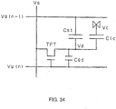
- Figure 34 shows an equivalent circuit of a pixel of the liquid crystal display wherein a storage capacitance Cst is formed between the preceding line of the scanning electrode and pixel electrode, and Figure 35 shows voltages of respective parts when driving the circuit.
- TFT denotes a thin film transistor
- Cgd denotes a capacitance between gate and drain
- Clc denotes a capacitance between the pixel electrode and common electrode (mainly, it is a capacitance formed by liquid crystal medium, besides, a capacitance formed by an other medium which is arrayed electrically in serial or electrically in parallel may be included.
- Vg(n-1) denotes a voltage of the preceding line scanning electrode
- Vg(n) denotes a voltage of the present line scanning electrode
- Vs or Vsig denotes a voltage of the picture signal
- Vd denotes a voltage of the pixel electrode
- Vc or Vcom denotes a voltage of the common electrode.
- the scanning electrode voltage Vg(n) of the present line varies as follows. First of all, the scanning electrode voltage Vg(n) of the present line becomes ON level Vgon. Next, the scanning electrode voltage Vg(n) of the present line becomes the compensation voltage level Vge(-) in order to turn off the scanning electrode of the present line and to apply overlapping voltage to the pixel electrode voltage Vd of the even number frame of the preceding line or latter line. After the application period of this compensation voltage Vge(-), the scanning electrode voltage Vg(n) of the present line becomes OFF level Vgoff. During the application period of the compensation voltage Vge(-), the scanning electrode voltage Vg(n-1) of the even number frame of the preceding line capacitively coupled with the present line has varied from Vge (+) to Vgoff.
- the scanning electrode voltage Vg(n) of the present line becomes compensation voltage Vge (-), and TFT becomes OFF level and turns to be OFF.
- the pixel voltage causes voltage drop of ⁇ V1 by the capacitive coupling of the capacitance formed in TFT and the total capacitance in the pixel.
- ⁇ V 1 ⁇ gd ⁇ ⁇ Vg 1 herein, ⁇ Vg1 describes the varying of the scanning electrode voltage Vg(n) shown in (Expression 2), ⁇ gd describes the capacitance ratio shown in (Expression 3), Cgd describes the gate-drain inter-electrode capacitance, Clc describes the liquid crystal capacitance, and Cst describes the storage capacitance.
- ⁇ Vge (+) describes the varying of the scanning electrode voltage Vg(n-1) of the preceding line shown by (Expression 5), ⁇ st describes the capacitive ratio shown by (Expression 6).
- the scanning electrode voltage of the present line varies from the compensation voltage Vge (-) to Vgoff.
- the pixel voltage causes the voltage varying of ⁇ V3 by the capacitive coupling of the capacitance formed in TFT and the total capacitance in the pixel.
- This varying voltage ⁇ V3 is shown by the following expressions (Expression 7).
- ⁇ V 3 ⁇ gd ⁇ ⁇ Vge ⁇
- ⁇ Vge (-) describes the varying of the scanning electrode voltage Vg(n) of the present line shown by (Expression 8), ⁇ gd describes the capacitive ratio shown by (Expression 3).
- ⁇ Vge ⁇ Vge ⁇ ⁇ Vgoff
- the pixel electrode voltage can be analyzed as the same. It becomes Vdo (+) shown by (Expression 10), and Vdo (+) will be maintained to the following scanning period.
- the picture signal voltage Vsig takes a positive value, and becomes Vsig (+).
- the compensation voltage Vge(+) is applied to the present line, the negative compensation voltage Vge (-) is overlapped to the scanning electrode of the odd number frame in preceding line.
- the voltage of a small amplitude (Vsig (+) and Vsig (-)) can be supplied to the picture signal electrode.
- the voltage of bigger amplitude (Vdo (+) and Vdo (-)) than this can be applied to the pixel electrode.
- the width of the voltage applied to the liquid crystal can be expanded to 10 volts or 15 volts, it becomes possible that the liquid crystal is driven by the voltage more than the permissible voltage.
- ⁇ V1 is treated as a feed-through voltage, however, a voltage fluctuation caused by the total variance of the scanning electrode voltage Vg of the present line can be included in the feed-through voltage.
- the feed-through voltage can be said as the merged value of the above-mentioned ⁇ V1 and ⁇ V3.
- the signal voltage whose polarity is inverted every one frame is charged to the pixel electrode.
- polarity may be arranged as the same through an entire screen and the polarity may be inverted by every one frame (field inversion method).
- there are other methods such as a method for inverting polarity every one line (line inversion method), a method for inverting polarity every one column (column inversion method), and a method for inverting polarity by a checkered pattern by combining the line inversion method and the column inversion method (dot inversion method). Drawing the charged pattern of the pixel by these methods yields Figure 36(a), Figure 36(b), Figure 36(c) and Figure 36(d) .
- the polarity of the picture signal applied to the picture signal electrode in one frame is constant.
- the polarity of the picture signal is inverted by each selection of the scanning electrode. In case of the field inversion method and the line inversion method, the polarity between the picture signal electrodes adjacent each other is the same, however, in the case of the column inversion method and the dot inversion method, the polarity becomes opposite.
- the pixel electrode voltage Vd of the present line varies all together from a negative voltage to a positive voltage in the case of the even number field, and varies all together from a positive voltage to a negative voltage in the case of the odd number field.
- the voltage of a common electrode fluctuates through the capacitance between the pixel electrode and the common electrodes (the capacitance of the liquid crystal is included) (the common electrode has a finite sheet resistance, on condition that the voltage on screen edge is fixed, the voltage in the screen inside will be slightly fluctuate.), the voltage charged in the pixel also receives the influence and is fluctuated, and the cross talk is generated.
- This is a cross talk that is generated by that the common electrode voltage Vc becomes different value before and after the scanning pulse applying because the common electrode voltage Vc is fluctuated and the voltage Vdo( ⁇ ) of the latched value of the pixel electrode does not become a value shown by (Expression 9) or (Expression 10).
- the column inversion method or the dot inversion method might be adopted for the above-mentioned reasons.
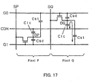
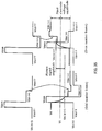
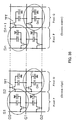
- Figure 38 is known as a pixel circuit structure to solve the above-mentioned problem. This is a structure described by page 195 to 198 of Proceedings of the Fourth International Display Workshop. The feature is to invert the layout of the pixel up and down every one row.
- the scanning electrode at the connection destination of the storage capacitor is different between adjacent pixels (scanning electrode G0 and G2). If different values of the compensation voltage are applied to the scanning electrode G0 and G2, different values of the overlapping voltage can be supplied to each pixel.
- the column inversion method or the dot inversion method for example, if a signal of a positive polarity is applied to the picture signal electrode S1 (or, Sn) and a signal of a negative polarity is applied to the picture signal electrode S2 (or, Sn+1), the overlapping voltage of the same polarity as the picture signal written in both pixels can be added by applying a compensation voltage Vge(-) to the scanning electrode G0 and applying a compensation voltage Vge(+) to the scanning electrode G2, so the effect of the amplitude increase can be achieved.
- the dot inversion method is taken as an example, a concrete scanning electrode signal drive waveform is shown in Figure 39 .
- the voltage applied to G0 is set as Vge(-)
- G2 is set as Vge(+).
- the scanning electrode G1 when the scanning electrode G1 is selected (period indicated by (E) in the figure), in this case, the picture signal electrode S1 is a negative polarity and the picture signal electrode S2 is a positive polarity, the voltage applied to G0 is set as Vge(+), and G2 is set as Vge(-).
- the period shown by (A) or (D) is the period which is preceded by one scanning period (an interval of a broken line in the figure is called one scanning period) from the period of (B) or (E).
- the scanning electrode G0 is selected and the scanning electrode G1 becomes a compensation voltage (the voltage of the preceding line of the G0 (it is not shown in the figure) also becomes a compensation voltage), and the voltage of G1 can be set as Ve(+) or Ve(-).
- the scanning electrode G2 is selected and the scanning electrode G1 becomes a compensation voltage (the voltage of the latter line of the G2 (it is not shown in the figure) also becomes a compensation voltage), and in this case, the same as above, the voltage of G1 can be set as Ve(+) or Ve(-).
- the voltage waveform of G0, G1 and G2 in the figure are obtained as a voltage waveform which should be applied to the scanning electrode.
- the dot inversion method is described above. In the same way, it is possible to consider the column inversion method.
- An irregular display is a problem along with a demand for increased size and a demand for high resolution of the liquid crystal display.
- the first cause of the irregular display is related to the distortion of the scanning voltage waveform caused by the CR time constant of the scanning lines, and the charge of the pixel electrode voltage becoming insufficient by the pixel position. Because the amount of a waveform distortion is different in the feeding power edge and the wiring terminal of the scanning voltage, the difference is generated in the pixel voltage, and this difference is seen as an irregular display. When the screen enlarges, the wiring resistance and the wiring capacitance grow, and the scanning time of the scanning lines shortens because of making to the high resolution, this irregular display becomes more remarkable. This is a problem for enlarging and increasing resolution.
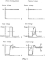
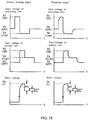
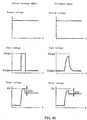
- Figure 40 is a figure simply describing the principle by which a charge becomes insufficient and irregular display is generated because of the distortion of the scanning voltage waveform caused by the CR time constant of scanning lines.
- the left side of this figure in order shows a signal voltage Vs, a scanning electrode voltage Vg, and a pixel electrode voltage Vd of a TFT connected with a feeding power edge pixel
- the right side of this figure in order shows a signal voltage Vs, a scanning electrode voltage Vg, and a pixel electrode voltage Vd of a TFT connected with a terminal pixel.
- the same signal voltage Vs is supplied to the signal electrode of each pixel through the respective picture signal electrode.
- the scanning voltage waveform is gradually distorted as it approaches the terminal by the influence of the scanning wiring time constant.
- the distortion is large, the scanning voltage waveform of the terminal pixel is distorted and does not reach Vg(ON) as shown by the second line in the right of Figure 40 .
- the pixel charge becomes insufficient and the pixel electrode voltage Vd does not reach Vs as shown by the third line.
- the decrease amount ( ⁇ Vb) of the pixel electrode voltage Vd by the capacitive coupling becomes smaller than that of the feeding power edge ( ⁇ Va) because the width of descending voltage of the scanning voltage waveform at the terminal is smaller than that at the feeding power edge.
- the irregular display is generated by the distortion of the scanning voltage waveform caused by the CR time constant of the scanning line.
- the second cause of the irregular display is the re-charge phenomenon caused by the shift of the transistor switching timing because of the distortion of the scanning voltage waveform.
- the pixel electrode voltages Vds become irregular according to the pixel position because the re-charge phenomenon is caused by the following reasons even though the charge is completely performed until the pixel electrode voltage Vd becomes the signal voltage Vs.
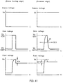
- Figure 41 is a figure which shows the reason easily.
- the uniform display is conducted through the entire screen, as shown in the first line, and the signal voltage Vs supplied from the picture signal line does not depend on the pixel position and is constant.
- the scanning voltage waveform at the terminal is distorted by the influence of the CR time constant though the scanning voltage waveform supplied from the scanning electrode is a rectangular wave in the feeding power edge.
- the scanning electrode Vg became a ON state, and it is assumed that the pixel electrode voltage Vd is charged until it reaches the signal voltage Vs.
- the voltage varying becomes steep and is generated quickly at an edge part of the screen near the feeding power edge part connected with the scanning signal drive circuit, and on the contrary, the voltage varying becomes gentle at the part far from the feeding power edge (the vicinity of center of the screen when feeding power is given from both right and left sides of the screen, the edge of the screen which is not the side connected with the scanning signal drive circuit when feeding power is given only from one side) because the distortion is caused in the waveform by the CR time constant of the scanning electrode.
- the scanning electrode voltage waveform shown in a near part and a far part from the feeding power edge becomes the one shown by the second line.
- the pixel electrode voltage Vd is almost equal to the picture signal voltage Vsig when completing the charge, the feed-through voltage is caused as Vg varies because of the capacitive coupling by Cgd of the circuit of Figure 34 .
- the feed-through voltage is shown by ⁇ Va shown by (Expression 11) regardless of the distance from the feeding power edge.
- the scanning electrode Vg changes to become a compensation voltage (for instance, Vge (-)).
- TFT does not become an OFF state at once when the scanning electrode voltage descends, and TFT becomes an OFF state for the first time when the the scanning electrode voltage passes the switching threshold (the voltage at which only the threshold voltage is higher than the picture signal electrode voltage). It is assumed that the switching at the terminal edge is delayed for the period of ⁇ t until the scanning electrode voltage reaches the threshold Vth of the transistor because of the distortion in the scanning electrode voltage waveform.
- the electric current will flow into the TFT in order to compensate for the voltage difference between the picture signal electrode and the pixel electrodes (between the source and the drain of TFT).
- the absolute value for an actual varying of the pixel electrode voltage Vd becomes smaller than
- the voltage waveform becomes gentle and the time span for the TFT turning to OFF becomes longer as the distance increases from the power feeding edge of the scanning signal drive circuit to the TFT, and ⁇ va' is considered to become large as the distance from the power feeding edge to the TFT becomes large.
- the electric current flowing at that moment is called re-charge current and the voltage difference ⁇ va' is called re-charge voltage.
- the pixel electrode voltage Vd at the terminal edge becomes ⁇ va' higher than that of the power feeding edge.
- the DC level of the pixel electrode voltage Vd shifts, and the irregular display such as flicker phenomenon is generated.
- the third cause of the irregular display is a problem that the transistor switching timing is shifted between the odd number frame and the even number frame caused by the distortion of the scanning voltage waveform, which becomes a problem in the case of adopting the method of the signal voltage inversion drive.
- the compensation voltage overlapped to the scanning voltage is different between the odd number frame and the even number frame.
- Vge (-) is overlapped as a compensation voltage in the odd number frame
- Vge (+) is overlapped as a compensation voltage in the even number frame.
- the re-charge period described in the above-mentioned second cause comes to differ if the transistor switching timing is different. As a result, according to the pixel position, the DC level of the pixel electrode voltage Vd shifts, and the irregular display such as flicker phenomenon is generated.
- the irregular display is observed as a stripe (stripes pattern) in the vertical direction because this irregular display is a light and shade pattern of the brightness of every column.
- the pixel P and the pixel Q in Figure 38 has the mirror plane symmetry structure, but the operation is not necessarily symmetric.
- the scanning electrode which becomes the compensation voltage when a certain scanning electrode is selected is located at the rear side in case of pixel P, and at the front side in case of pixel Q when the scanning direction is defined as a direction from top to bottom.
- the fourth cause of the irregular display is a problem that the transistor switching timing is shifted by the difference whether the signal voltage applied to the pixel electrode is a positive direction or a negative direction.
- the liquid crystal display adopts either the above-mentioned column inversion methods or the dot inversion method, and if there is a distortion in the scanning voltage waveform, because of the difference of whether the signal voltage is applied in a positive direction and the pixel electrode voltage Vd is a positive charge or the signal voltage is applied in a negative direction and the pixel electrode voltage Vd is a negative charge, the transistor switching timing shifts.
- the transistor switching voltage just passes the voltage that is higher by a certain threshold voltage than the picture signal electrode voltage Vsig, the transistor is turned off.
- the transistor switching timing comes to differ according to whether the picture signal electrode voltage Vsig is positive or negative.
- the re-charge period described in the above-mentioned second cause and the third cause comes to differ if the transistor switching timing is different.
- the DC level of the pixel electrode voltage Vd shifts, and the irregular display such as flicker phenomenon is generated.
- Figure 42 is a diagram showing the above-mentioned third cause and fourth cause.
- the waveform seen when the scanning voltage descends from Vgon is different depending whether the compensation voltage is the positive compensation voltage Vge(+) in the even number frame or the compensation voltage is the negative compensation voltage Vge(-) in the odd number frame.
- the threshold value at which the transistor becomes off is different depending whether the charge of the pixel electrode voltage Vd is a positive charge or a negative charge, the timing when the transistor turns to off shifts between the four patterns ⁇ t1 to ⁇ t4.
- the technology disclosed in the JPA Tokkai-Hei 5-232509 is known to ease the above-mentioned second irregular display cause.
- the value of the storage capacitance which is formed in parallel to each pixel capacitance, increases at the power feeding edge of the scanning electrode and decreases at the terminal edge of the scanning electrode according to the position of the pixel, and the charging property of the terminal side pixel is improved and the charging property is adjusted to be uniform.
- the feed-through voltage at the terminal side pixel is increased to the re-charge voltage, which is higher than the feed-through voltage at the power feeding edge, and displaying is adjusted to be uniform.
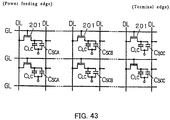
- FIG 43 is a circuit diagram showing the structure of the circuit shown in the JPA Tokkai-Hei 5-232509 .
- 201 denotes a thin film transistor (TFT)
- GL denotes a scanning electrode
- DL denotes a picture signal electrode
- CLC denotes a pixel capacitance
- CSCA - CSCC denote storage capacitance which are formed between the pixel electrode and the common electrode.
- the storage capacitance CSCA - CSCC become large at the power feeding edge of the scanning electrode (CSCA) and become small at the terminal edge (CSCC).
- a display apparatus of the present invention is defined in claim 1.
- This embodiment makes it possible to compensate the deviation of the DC level of the pixel electrode voltage, to reduce a flicker, and to reduce the difference of the coupling voltage overlapped to the pixel electrode voltage and achieve uniform brightness.
- This embodiment makes it possible to maintain the liquid capacitance (opposite electrode-pixel electrode inter-electrode capacitance) constantly, and increase the first capacitance ratio ⁇ gd continuously or in stages according to the distance from the power feeding edge of the scanning electrode so that the rate of aperture does not fluctuate by the pixel position.
- both the storage capacitance and a capacitance formed between the opposite electrode and the pixel electrode decrease according to the distance from the power feeding edge of the scanning electrode.
- This embodiment makes it possible to maintain the gate-drain inter-electrode capacitance Cgd, increase the first capacitance ratio ⁇ gd continuously or in stages according to the distance from the power feeding edge of the scanning electrode.
- the merit in maintaining the capacitance Cgd between gate-drain inter-electrode to be constant and controlling an other parameter is that it is easier to control the first capacitance ratio ⁇ gd by varying other parameters than to control the first capacitance ratio ⁇ gd by varying the first capacitance Cgd when the Cgd is small.
- the area of the shading part for example, a black matrix part
- the rate of aperture it is preferable to put the area of the shading part (for example, a black matrix part) constantly to maintain the rate of aperture to be constant even if the pixel configuration varies.
- each capacitance element of the pixel is set so the second capacitance ratio ⁇ st shown by (Expression 13) is substantially constant.
- ⁇ st Cst / Ctot
- This embodiment makes it possible to reduce the difference of the coupling voltage overlapped to the pixel electrode voltage and achieve uniform brightness.
- each capacitance element of the pixel is set so the second capacitance ratio ⁇ st increases continuously or in stages according to the distance from the power feeding edge of the scanning electrode.
- this embodiment makes it possible to reduce the difference of the coupling voltage overlapped to the pixel electrode voltage and achieve uniform brightness.
- the display medium is a liquid crystal.
- the display apparatus further comprises a means for overlapping a voltage to the driving circuit of the scanning signal via the storage capacitance.
- the driving circuit of the scanning signal comprises the output voltage of more than four values.
- the voltage via the storage capacitance is applied to the pixel electrode after applying the voltage via the switching element.
- This embodiment makes it possible to reduce the influence of the time constant of the scanning electrode in the capacitively coupled driving method and to drive the liquid crystal display of large-scale and high resolution by low voltage.
- any configuration of the display apparatus may further comprise a second switching element wherein the pixel electrode combines the gate electrode of the second switching element or the pixel electrode is connected with the gate electrode of the second switching element.
- the present invention can be applied to the display apparatus comprising 2 switching elements such as an organic electro-luminescence display apparatus.
- Embodiments of the display apparatus of this invention are shown from Embodiment 1 to Embodiment 6, Illustrative Embodiments of one example display apparatus are shown from Illustrative Embodiment 7 to Illustrative Embodiment 11, Ilustrative Embodiments of a second example display apparatus are shown from Illustrative Embodiment 12 to Illustrative Embodiment 16, and Illustrative Embodiments of a a third example display apparatus are shown from Illustrative Embodiment 17 to Illustrative Embodiment 20.
- the pixel electrode voltage is described as Vd
- the picture signal is described as Vs or Vsig
- the common voltage is described as Vc or Vcom.
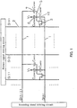
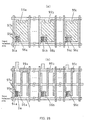
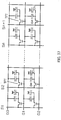
- Fig. 1 is a circuit diagram showing a basic configuration of the liquid crystal display apparatus according to Embodiment 1 of the present invention.
- 1 denotes a scanning electrode
- 2 denotes a picture signal electrode wherein thin film transistor (TFT) 3 is formed at the intersection as a TFT switching element.
- the gate electrode of TFT 3 is connected with the scanning electrode 1
- the source electrode is connected with the picture signal wiring 2
- the drain electrode is connected with the pixel electrode 5 respectively.
- the pixel comprises two capacitor 6 and 7.
- a liquid crystal capacitor 6 (Clc) is formed between the picture electrode 5 and the opposite electrode, and the liquid crystal is driven by a voltage applied to the both ends.
- the opposite electrode voltage Vc is supplied to the opposite electrode.
- Storage capacitor 7(Cst) is formed in parallel with the liquid crystal capacitor 6. When the charge leaks from the liquid crystal capacitor 6, this parallel capacitor compensates for this leakage and stabilizes the operation of the liquid crystal.
- the storage capacitor 7 is formed between the electrode 5 and the scanning electrode 1 of the preceding line.
- the gate-drain inter-electrode capacitor 10 (Cgd) is formed between the gate and the drain of TFT.
- the liquid crystal display apparatus has pixels arranged in the matrix, in the Fig. 1 , the pixel of the "n"th line and the surrounding electrode wiring are shown, and other parts are omitted.
- G(n-1) denotes a scanning electrode of the "n-1" line
- G(n) denotes a scanning electrode of the "n”th line.
- S(1) denotes a picture signal wiring of the first line
- S(P) denotes a picture signal wiring of the "P"th line.
- Both of the storage capacitor (Cgd) and gate-drain inter-electrode capacitor (Cst) are gradually enlarged from the power feeding edge of the scanning electrode (left side in Fig. 1 ) to the terminal edge (right side in Fig. 1 ).
- the first capacitance ratio ⁇ gd shown in the (Expression 22) is adjusted as being gradually enlarged from the power feeding edge of the scanning electrode to the terminal edge.
- ⁇ gd Cgd / Ctot
- ⁇ st Cst / Ctot wherein, Ctot denotes all capacitor connected with pixel electrode.
- Ctot usually is calculated as Cst+Cgd+Clc, and when there are other capacitances in the pixel electrode, Ctot includes such other capacitances.
- the capacitance formed in parallel with the gate-drain inter-electrode capacitor 10 (Cgd) is included in the Cgd.
- This liquid crystal display apparatus is driven as follows.
- the shape of the driving waveform supplied to each electrode is the one shown in Fig. 35 as in the conventional capacitively coupled driving method. That is, first of all, the on-state voltage is applied to the scanning electrode G(n) of "n"th line, and TFT turns to ON and the pixel is charged. Next, the scanning voltage becomes off level and TFT turns to OFF, and then a step voltage is applied to the scanning electrode G(n-1) of the preceding line and overlapping the coupling voltage through the storage capacitor 7.
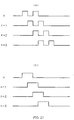
- Fig. 2 and Fig. 3 are the diagram showing the time varying of the gate voltage (scanning electrode voltage) and the pixel electrode voltage when capacitively coupled driving is conducted through the storage capacitance on the scanning electrode of the preceding line.
- the gate voltage applied to the TFT (present line) and the gate voltage related to the capacitance coupling (preceding line) are shown.
- the polarity of the pixel voltage is inverted between pixels adjacent upstream and downstream, a voltage varying of the odd number frame where the pixel is charged to a positive voltage is shown in Fig. 2 , and a voltage varying of the even number frame where the voltage polarity is inverted is shown in Fig. 3 .
- the pixel is once charged to Vs(+) in the positive charge period and charged to Vs(-) in the negative charge period.
- the gate voltage decreases, the pixel electrode voltage is varied by the downward coupling voltage ( ⁇ V1 of Fig. 2 or ⁇ V1' of Fig. 3 ).
- Adjusting the first capacitance ratio ⁇ gd to be gradually enlarged from the power feeding edge of the scanning electrode to the terminal edge has the effect that the in-plane distribution of ⁇ V1 and ⁇ V1' become uniform.
- the coupling voltage ⁇ V2 or ⁇ V2 ' is overlapped to the pixel electrode voltage through the storage capacitance. Assuming ⁇ st to be an substantially constant in the pixel on the same scanning electrode has the effect that the in-plane distribution of ⁇ V2 and ⁇ V2' become uniform.
- the effect for adjusting the first capacitance ratio ⁇ gd to be gradually enlarged from the power feeding edge of the scanning electrode to the terminal edge is as follows.
- Fig. 4 explains these reasons.
- the source voltage supplied from the picture signal line does not depend on the pixel and is constant.
- the waveform of the gate voltage supplied from the scanning electrode is a rectangular wave in the feeding power edge, however, it is distorted by the influence of the wiring time constant in the terminal edge as shown in Fig. 4 .
- ⁇ Va shows the sum of ⁇ V1 and ⁇ V3.
- the TFT becomes the OFF state at once, and pixel electrode voltage Vd settles down in Vs- ⁇ V1.
- the time of ⁇ t is necessary by the time the TFT becomes the OFF state as shown in Fig. 4 because there is a distortion in the gate voltage waveform at the pixel on the terminal edge. Meanwhile, the pixel electrode voltage Vd is charged again toward Vs.
- the pixel electrode voltage on the terminal edge varies as shown by 41 in Fig. 4 and it becomes the voltage that is higher by ⁇ V' high from the voltage at the power feeding edge. As a result, the DC level of the pixel electrode voltage becomes different between the power feeding edge and the terminal edge.
- the liquid crystal display apparatus of this configuration enlarges the first capacitance ratio ⁇ gd on the terminal edge of the scanning electrode, ⁇ V1 enlarges in the terminal edge.
- the first capacitance ratio ⁇ gd is varied in order to enlarge the decrease in voltage by the capacitance coupling at the terminal edge when the gate voltage decreases, and the varying of the pixel electrode voltage moves from the line of 41 to the line of 42 shown in Fig. 4 . Therefore, the final voltage level becomes equal at the power feeding edge and the terminal edge, an irregular display for which the flicker etc. are assumed to be a cause is not generated, and the uniform display can be achieved.
- the degree by which the first capacitance ratio ⁇ gd varies can be obtained according to the computer simulation etc. of each part of the voltage waveform.
- Vg(+) denotes an overlapped positive modulation voltage
- Vg(-) denotes an overlapped negative modulation voltage
- the second capacitance ratio ⁇ st is substantially made constant through the pixels on the same scanning electrode, and the overlapping voltage ⁇ V2 or ⁇ V2 ' does not depend on the pixel and becomes constant. It is necessary for respective voltage of Vg(high), Vg(OFF), and Vg(low) to be set in a range where the transistor of the preceding scanning line does not become ON status in order not to vary the pixel electrode voltage of the preceding line.
- the liquid crystal display apparatus of this Embodiment 1 is composed to satisfy the following three conditions.
- both the voltage varying by the coupling voltage when the gate voltage of the present line descends ( ⁇ V1 of Fig. 2 and ⁇ V1' of Fig. 3 ), and the overlapping voltage by the capacitively coupled driving ( ⁇ V2 of Fig. 2 and ⁇ V2' of Fig. 3 ) are made to be uniform through the screen.
- Embodiment 1 an ideal Embodiment of this invention is described. However, when there are a restriction in the design etc., among three conditions concerning the capacitance shown in Embodiment 1, the effect to some extent can be achieved in practice only by the rest two of three conditions except the condition that "(3) The second capacitance ratio ⁇ st in pixel on the same scanning electrode is configured to be substantially constant".
- Embodiment 2 shows a configuration wherein the storage capacitance and the gate-drain inter-electrode satisfies the remaining two conditions.
- the condition (2) is satisfied by using the configuration where the gate-drain inter-electrode (Cgd) is gradually enlarged from the power feeding edge of the scanning electrode to the terminal edge, or in addition to that configuration, the configuration where the storage capacitance (Cst) is gradually reduced is used.
- Embodiment 2 the condition (2) is satisfied by adjusting both the storage capacitance (Cst) and the gate-drain inter-electrode capacitance (Cgd) to be gradually enlarged from the power feeding edge of the scanning electrode to the terminal edge.
- ⁇ st is defined by (Expression 23).
- both the storage capacitance (Cst) and the gate-drain inter-electrode capacitance (Cgd) are gradually enlarged from the power feeding edge of the scanning electrode to the terminal edge.
- This method gradually enlarges the first capacitance ratio ⁇ gd from the power feeding edge of the scanning electrode to the terminal edge by the varying of the gate-drain inter-electrode capacitance, and the varying of the second capacitance ratio ⁇ st accompanying the enlargement of ⁇ gd is canceled or reduced by the varying of the storage capacitance.
- Embodiment 3 gradually enlarges the first capacitance ratio ⁇ gd from the power feeding edge of the scanning electrode to the terminal edge by the varying of the storage capacitance, and the varying of the second capacitance ratio ⁇ st accompanying the enlargement of ⁇ gd is canceled or reduced by the varying of the gate-drain inter-electrode capacitance.
- the pixel configuration shown in Fig.1 of the liquid crystal display apparatus in this Embodiment has a configuration which satisfies the following three conditions.
- the liquid crystal display apparatus of this Embodiment 3 is driven in the same manner as that of Embodiment 1.
- both the voltage varying by the coupling voltage when the gate voltage of the present line decreases ⁇ V1 of Fig. 2 and ⁇ V1' of Fig. 3
- the overlapping voltage by the capacitively coupled driving ⁇ V2 of Fig. 2 and ⁇ V2' of Fig. 3
- Embodiment 3 an ideal Embodiment of this invention is described. However, when there are restrictions in the design etc., among three conditions concerning the capacitance shown in Embodiment 3, the effect to some extent can be achieved in practice only by the rest two of three conditions except the condition that "(3) The second capacitance ratio ⁇ st in pixel on the same scanning electrode is configured to be substantially constant".
- Embodiment 4 shows a configuration wherein the storage capacitance and the gate-drain inter-electrode satisfies the remaining two conditions.
- condition (2) is satisfied by using the configuration where the storage capacitance (Cst) is gradually reduced from the power feeding edge of the scanning electrode to the terminal edge, or in addition to that configuration, the configuration where the gate-drain inter-electrode (Cgd) is gradually enlarged is used.
- Embodiment 4 the condition (2) is satisfied by adjusting both the storage capacitance (Cst) and the gate-drain inter-electrode capacitance (Cgd) are gradually reduced from the power feeding edge of the scanning electrode to the terminal edge.
- ⁇ st is defined by (Expression 23).
- Embodiment 5 show an example where the display apparatus shown either in Embodiment 1 to Embodiment 4 is applied to the In-Plane Switching mode (IPS) liquid crystal display apparatus.
- IPS In-Plane Switching mode
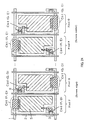
- Fig. 31 is a diagram showing a cross section of a IPS liquid crystal display apparatus
- Fig. 32 is a diagram showing a plane configuration of one pixel of the IPS liquid crystal display apparatus.
- the center part of Fig. 31 shows a cross section structure along A-A' line shown in Fig. 32 .
- 11 and 12 are substrates made of glass etc.
- 11 denotes an array substrate formed with TFTs and electrodes connected with it
- 12 denotes an opposite substrate opposing the array substrate 11.
- a liquid crystal 13 is inserted between two substrates, and the both ends are sealed by seal 17.
- 14 and 15 denote polarized light boards to display polarized light
- 19 denotes a color filter to conduct color displaying.
- the color filter is formed on the opposite substrate 12 side, but it may be formed on the array substrate 11 side.
- the scanning electrode 1 and the common electrode 4 are formed by the first conductive layer on the array substrate 11, and the insulation film 18 covers the array substrate 11.
- the pixel electrode 5 is formed by the second conductive layer on the insulation film 18.
- the overlap part with the scanning electrode 1 in the preceding line comprises the storage capacitance 7 (Cst).
- the overlap part between the pixel electrode 5 and the scanning electrode 1 in the present line comprises the scanning electrode-pixel electrode capacitance (Cgd).
- the branch part 4A is formed in the common electrode 4. This faces in parallel to the pixel electrode 5, and works as an opposite electrode to apply the electric field to the liquid crystal layer.
- the capacitance between the pixel electrode 5 and the common electrode 4 comprises the common electrode-pixel electrode capacitance Clc, and the Clc includes both of the capacitance through the liquid crystal layer and the capacitance formed by geometrical overlap of both electrodes.
- the capacitance through the liquid crystal layer is difficult to calculate by using the expression, but it may be obtained by measurement, or may be obtained by simulation.
- TFT3 is composed of the electrode in 9 and three semiconductor parts, normally the gate electrode connected with the scanning electrode 1, the source electrode connected with the picture signal wiring 2, and the drain electrode connected with the pixel electrode 5 respectively.
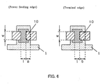
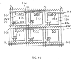
- Fig. 5 is a circuit diagram showing a configuration of a pixel of a liquid crystal display apparatus according to Embodiment 5.
- Fig. 6 is an enlargement of the TFT part shown in Figure 5 .
- Fig. 5 1 denotes a scanning electrode, 2 denotes a picture signal electrode, 3 denotes a TFT, 5 denotes a pixel electrode, and 51 denotes an opposite electrode in which the array of the liquid crystal is controlled by the electric field generated therebetween with the pixel electrodes 5, and the displaying is operated.
- the opposite electrode 51 is connected mutually with the common electrode 52.
- FIG. 5 and Figure 6 corresponds to the liquid crystal display apparatus explained in Embodiment 1 and Embodiment 2, both the gate-drain capacitance and the storage capacitance at the terminal edge are enlarged more than those at the power feeding edge.
- TFT property becomes uniform, and further uniform displaying can be conducted.
- the shape of the gate part in the TFT is adjusted to reduce width (width a) of the overlap part on the power feeding edge side, and to enlarge width (width b) of the overlap part on the terminal edge side. In this way, the pattern to obtain the desiring gate-drain capacitance can be easily designed.
- Embodiment 6 show an example where the display apparatus shown either in Embodiment 1 to Embodiment 4 is applied to the twisted nematic (TN) mode liquid crystal display apparatus.
- Fig. 7 is a circuit diagram showing a configuration of the pixel of a liquid crystal display apparatus according to Embodiment 6.
- Fig. 5 The difference from Fig. 5 is that the whole of the pixel area is almost covered with pixel electrode 5, there is an opposite electrode on the opposite substrate though it is not shown in the figure, the array of the liquid crystal is controlled by the electric field generated therebetween with the pixel electrodes 5, and the displaying is operated.
- the enlargement of the TFT part is the same as shown in Figure 6 described in the above-mentioned Embodiment.
- the part where the pixel electrode 5 and the gate 73 of TFT overlap comprises the gate-drain capacitance 10
- the part where the pixel electrode 5 and the scanning electrode 1 in the preceding line overlaps forms the storage capacitance 7.
- both the gate-drain capacitance and the storage capacitance at the terminal edge are enlarged more than those at the power feeding edge.
- the shape of the gate part in the TFT is adjusted to reduce width (width a) of the overlap part on the power feeding edge side, and to enlarge width (width b) of the overlap part on the terminal edge side. In this way, the pattern to obtain the desiring gate-drain capacitance can be easily designed.
- Embodiment 5 and Embodiment 6 a concrete configuration of the pixel corresponding to the liquid crystal display apparatus of Embodiment 1 and Embodiment 2 is explained. This also can be applied to the liquid crystal display apparatus of Embodiment 3 and Embodiment 4.
- both the gate-drain capacitance and the storage capacitance at the terminal edge side should be reduced less than those at the power feeding edge side. It may be considered by reversing the configuration between the power feeding edge side and the terminal edge side shown in Figure 5 , 6 and 7 .
- the Illustrative Embodiment of one example display apparatus is shown.
- the display apparatus of this Illustrative Embodiment 7 includes the first storage capacitance between the pixel electrode and the scanning electrode among the scanning electrodes except the scanning electrode in the present line, and includes the second storage capacitance between the pixel electrode and the storage capacitance electrode.
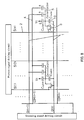
- Fig. 8 is a diagram showing a basic configuration of the liquid crystal display apparatus according to Illustrative Embodiment 7.
- 1 denotes a scanning electrode
- 2 denotes a picture signal electrode wherein thin film transistor (TFT) 3 is formed at the intersection as a switching element.
- the gate electrode of TFT 3 is connected with the scanning electrode 1
- the source electrode is connected with the picture signal wiring 2
- the drain electrode is connected with the pixel electrode 5 respectively.
- the capacitance of the pixel is comprised of three capacitors 6, 7 and 8.
- the liquid capacitance 6 is formed between the pixel electrode 5 and the opposite electrode through the liquid crystal, and the liquid crystal performs the operation according to the voltage applied to both ends.
- the opposite electrode voltage Vcnt is supplied to the opposite electrode.
- the first storage capacitance 7 is formed between the pixel electrode 5 and the scanning electrode 1 of the preceding line
- the second capacitance 8 is formed between the pixel electrode 5 and the pixel electrode 5 and the common electrode 4.
- the gate-drain capacitance Cgd exists between the gate and the drain in TFT.
- Fig. 8 shows the electrode wiring for the pixels of "n"th line and the surrounding, other parts are omitted.
- G(n-1) is a scanning electrode of the "n-1"th line
- G(n) is a scanning electrode of "n”th line
- COM(n-1) is a common electrode of the "n-1”th line
- COM(n) is a common electrode of "n”th line.
- S(1) is a picture signal wiring of the first row
- S(p) is a picture signal wiring of "p"th row (final row).
- the opposite electrode and the common electrode 4 are shown separately in Figure 8 , in the case of IPS, the opposite electrode and the common electrode 4 are configured as a body. And, the part where the pixel electrode 5 and the common electrode 4 oppose through the liquid crystal becomes the liquid crystal capacitance 6, and the part where the pixel electrode 5 and the common electrode 4 oppose through the insulating layer etc. becomes the second storage capacitance 8.
- This liquid crystal display apparatus is driven as shown next.
- the shape of the driving waveform supplied to each electrode is the one shown in Fig. 35 as with the conventional capacitively coupled driving. That is, first, the ON-state voltage is applied to the scanning electrode G(n) of "n"th line, TFT becomes ON status and the pixel is charged. Next, the scanning voltage turns to be OFF level and TFT becomes OFF status. Afterwards, the step voltage is applied to the scanning electrode G(n-1) in the preceding line and overlaps coupling voltage through first storage capacitance 7.
- ⁇ st1 is the fourth capacitance ratio
- Ctot denotes all capacitance connected with pixel electrode. Normally, Ctot usually is calculated as Cst1+Cst2+Cgd+Clc, and when there are other capacitances in the pixel electrode, Ctot includes such other capacitances. In addition, the capacitance formed in parallel with the gate-drain inter-electrode capacitance 10 (Cgd) is included in the Cgd.
- Each pixel and the storage capacitance arranged one by one in the pixel conventionally are divided into two parts, and the feature of the liquid crystal display apparatus of this illustrative Embodiment 7 is that one side is formed on the common wiring, the other side is formed on the scanning wiring of the preceding line and the capacitively coupled driving uses the storage capacitance in the scanning wiring of the preceding line.
- the pixel charge time can be kept long, the re-charge time can be decreased, the irregular brightness caused by pixel charge shortage can be decreased, and the flicker caused by the difference of the pixel re-charge can be decreased.
- Fig. 9 is a diagram showing the degree of the brightness decrease in the terminal pixel because of the panel size expansion.
- the brightness of the pixel of the power feeding edge is assumed to be 100%, and the result of simulating the brightness of the pixel of the terminal edge is shown.
- the number of pixels is 720(length) ⁇ 1280(side), and the case that the liquid crystal display apparatus of the conventional technology is driven by the capacitively coupled driving and the case that the liquid crystal display apparatus of the present invention are compared.
- the storage capacitance (total sum) on both sides are assumed to be equal.
- the shown data of the liquid crystal display apparatus of this invention are the case when the storage capacity is divided into two parts, with the one part being formed on the common wiring and the other part being formed on the scanning wiring of the preceding line.
- the brightness of the pixel of the terminal edge becomes 95% in the corner for 15 inch types (381mm) and an irregular display begins to stand out, however, the uniform display can be achieved in the corner for up to 27 inch types (686mm) with a liquid crystal display apparatus of this invention.
- the generation of the flicker by the capacitance coupling phenomenon is controlled by decreasing the scanning waveform distortion.
- the liquid crystal display apparatus of this illustrative Embodiment 7 is effective for the high resolution liquid crystal display apparatus.
- the charge time will decrease per one scanning line. In this case, the charge becomes short on the scanning electrode is the terminal edge, and an irregular display is generated the same as for the display enlargement.
- the liquid crystal display of this illustrative Embodiment 7 decreases the time constant of the scanning wiring by the same principle as the above-mentioned, the pixel charge time can be kept long by extending the effective charge time of the terminal pixel, and the irregular brightness due to pixel charge shortage can be decreased.
- the liquid crystal display of this illustrative Embodiment 7 can decrease the re-charge time, and the flicker caused by the difference of the pixel re-charge can be decreased.
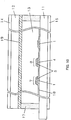
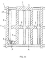
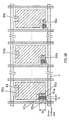
- Fig. 10 is a diagram of a cross section of the liquid crystal display apparatus according to illustrative Embodiment 8
- Fig. 11 is a circuit diagram showing a configuration of a pixel of a liquid crystal display apparatus shown in Fig. 10 .
- the center part of Fig. 10 shows the sectional structure along line A-A' shown in the Fig. 11 .
- Fig. 10 , 11 and 12 are substrates made of glass etc.
- 11 denotes an array substrate formed with TFTs and electrodes connected with it
- 12 denotes an opposite substrate opposing to the array substrate 11.
- a liquid crystal 13 is inserted between two substrates, and the both ends are sealed by seal 17.
- 14 and 15 denote polarized light boards to display polarized light
- 19 denotes a color filter to conduct color displaying.
- the color filter is formed on the opposite substrate 12 side, but it may be formed on the array substrate 11 side.
- the scanning electrode 1 and the common electrode 4 are formed by the first conductive layer on the array substrate 11, and the insulation film 18 covers the array substrate 11.
- the pixel electrode 5 is formed by the second conductive layer on the insulation film 18. As shown in Fig. 11 , the pixel electrode 5 overlaps with the common electrode 4 and the scanning electrode 1 in the preceding line.
- the overlap part between the pixel electrode 5 and the scanning electrode 1 of the preceding line comprises the storage capacitance 7 (Cst), and, the overlap part between the pixel electrode 5 and the common electrode 4 comprises the second storage capacitance 8.
- the branch part 4A is formed in the common electrode 4. This faces in parallel to the pixel electrode 5, and works as an opposite electrode to apply the electric field to the liquid crystal layer.
- the common electrode 4 is the same as the opposite electrode.
- TFT3 is composed of the electrode in 9 and three semiconductor parts, normally the gate electrode connected with the scanning electrode 1, the source electrode connected with the picture signal wiring 2, and the drain electrode connected with the pixel electrode 5 respectively.
- the fourth value of capacitance ratio ⁇ st1 described by (Expression 26) or (Expression 27) can be moderated and adjusted, the generation of the lateral stripes can be suppressed by easing the influence that the voltage fluctuation of the scanning electrode in preceding line has on the pixel electrode voltage.
- An electricity-optical characteristic of the IPS liquid crystal varies from the dark status to the bright status by the width of the voltage of about 2.5 volts.
- the width of the voltage per one gradation is about 10mV.
- the width of the on/off output voltage of the scanning drive IC is about from 20 to 30 volts, and the deflection of 0.1 percent corresponds to 20-30mV.
- the value of Cst1/(Cst1+Cst2+Cgd+Clc) becomes 0.5 or less, preferably 0.3 or less, the output deflection of the 0.1 percent of the scanning side drive IC can be reduced to less than the width of the voltage of one gradation, and it is possible to cancel the lateral stripes.
- the liquid crystal capacitance is about 1/10 compared with the twisted nematic mode used widely at present. Therefore, big storage capacitance is required from the TN type to stabilize the pixel electrode voltage.
- the area will become insufficient according to circumstances, the expansion of the width of the line is required, and the aperture ratio will be deteriorated.
- the configuration of this illustrative Embodiment 8 is used, because the pixel electrode voltage fluctuation can be prevented by forming enough storage capacitance without deteriorating the aperture ratio, a bright, high-quality display can be obtained.
- any method can show the effect explained in illustrative Embodiment 8.
- these include a configuration in which the pixel electrode 21 and the opposite electrode 22 are on same substrate 23 as shown by Fig. 12(a) , and a configuration in which liquid crystal is operated by the parallel or skewed electric field against the substrate by forming the opposition electrode 22 onto the opposite substrate 24 shown by Fig. 12(b) or (c) .
- the pixel electrode 21 and the opposite electrode 22 applying the electric field to the liquid crystal 25 do not form a parallel, monotonic capacitance, and the liquid crystal capacitance is small compared with the TN type as shown in Fig.
- the third capacitance ratio ⁇ gd1 is gradually enlarged from the power feeding edge of the scanning electrode to the terminal edge.
- ⁇ gd 1 Cgd / Ctot
- Ctot denotes all capacitance connected with pixel electrode. Normally, Ctot usually is calculated as Cst1+Cst2+Cgd+Clc, and when there are other capacitances in the pixel electrode, Ctot includes such other capacitances. In addition, the capacitance formed in parallel with the gate-drain inter-electrode capacitance 10 (Cgd) is included in the Cgd.
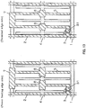
- Fig. 13 is one example showing the configuration in which the first storage capacitance 7 (Cst 1) and the second storage capacitance 8 (Cst 2) become large at the power feeding edge side and become small at the terminal edge side by varying the shape of the pixel electrode 5.
- the third capacitance ratio ⁇ gd1 becomes small at the power feeding edge side and becomes large at the terminal edge side because Cst1 and Cst2 are included in the denominator of the (Expression 28).
- Fig. 41 used for explaining the problem in the prior art, that when the distortion is caused in the scanning voltage in the liquid crystal display apparatus employing the TFT, even when the charge is completely performed, no uniformity is caused in the pixel voltage for the following reason.
- the TFT becomes an OFF state at once and the pixel electrode voltage Vd settles down in Vs- ⁇ V1.
- the gate voltage waveform supplied from the scanning electrode is distorted by the influence of the wiring time constant at the terminal edge.
- the time of ⁇ t will be needed by the time the TFT becomes a OFF state as shown in Figure 41 is middle part, the pixel electrode voltage Vd is charged to Vs again during ⁇ t, a part of feed-through voltage ⁇ va1 is canceled, so it becomes voltage that only ⁇ Va1' is high as right part of Fig. 41 .
- the DC level of the pixel electrode voltage Vd becomes a different value between the power feeding edge and the terminal edge, and therefore display irregularity such as flicker phenomenon is generated.
- the pixel electrode voltage in the terminal edge settles down with the pixel electrode voltage on the power feeding edge in the place where it becomes equal to the pixel electrode voltage on the terminal edge when pixel voltage varying ⁇ V' by the re-charge during ⁇ t is subtracted.
- the level that the pixel electrode voltage finally reaches becomes equal between the power feeding edge and the terminal edge display irregularity such as flicker is not caused, and the uniform display can be achieved.
- the degree by which the third capacitance ratio ⁇ gd1 varies can be obtained according to the computer simulation etc. of each part of the voltage waveform.
- the gate-drain inter-electrode capacitance (Cgd) for instance, in Fig. 13 , the area of the overlapping part of the gate and drain of the TFT is changed. In short, it is enough that at least one of the first storage capacitance (Cst1), the second storage capacitance (Cst2), the gate-drain inter-electrode capacitance (Cgd), and the liquid crystal capacitance (Clc) varies so that ⁇ gd1 becomes large at the terminal edge side.
- the display apparatus of illustrative Embodiment 10 is a display wherein the capacitance of each pixel is set as the fourth capacitance ratio ⁇ st1 defined by the (Expression 30) shown in illustrative Embodiment 9 becomes constant between the pixel on the same scanning electrode.
- ⁇ st 1 Cst 1 / Ctot
- Ctot denotes all capacitance connected with pixel electrode. Normally, Ctot usually is calculated as Cst1+Cst2+Cgd+Clc, and when there are other capacitances in the pixel electrode, Ctot includes such other capacitances. In addition, the capacitance formed in parallel with the gate-drain inter-electrode capacitance (Cgd) is included in the Cgd.
- Fig. 15 and Fig. 16 are the diagrams showing the time variation of the gate voltage (scanning electrode voltage) and the pixel electrode voltage when capacitively coupled driving is conducted through the storage capacitance on the scanning electrode of the preceding line. Both of the gate voltage applied to the TFT connected with this pixel (present line) and the gate voltage related to the capacitive coupling (preceding line) are considered as the gate voltage.
- the polarity of the pixel voltage is inverted between pixels adjacent upstream and downstream. A voltage varying of the odd number frame where the pixel is charged to a positive voltage is shown in Fig. 15 , and a voltage varying of the even number frame where the voltage polarity is inverted is shown in Fig. 16 .
- the pixel is once charged to Vs(+) in the positive charge period and charged to Vs(-) in the negative charge period.
- the gate voltage decreses, the pixel electrode voltage is varied by the downward coupling voltage ( ⁇ V1 of Fig. 15 or ⁇ V1' of Fig. 16 ). This vary amount of the scanning voltage at the power feeding edge and the terminal edge finally reach the same level by the configuration shown in illustrative Embodiment 9.
- the voltage of the preceding line has varied in the step shape, and the coupling voltage ⁇ V2 or ⁇ V2' is overlapped to the pixel electrode voltage through the first storage capacitance.
- This overlapped voltage value becomes the product of multiplying the fourth capacity ratio ⁇ st1 shown by (Expression 30) by the amount of variation of the gate voltage of the preceding line.
- At least two of four capacitances shown above varies from the power feeding edge pixel to the terminal edge pixel, ⁇ gd1 shown by (Expression 28) is enlarged from the power feeding edge to the terminal edge and ⁇ st1 shown by (Expression 30) becomes constant.
- the coupling voltage V2 and V2' overlapped to the pixel electrode voltage can be constant regardless of the position of the pixel, and further uniform display can be achieved comparing with the liquid crystal display apparatus of illustrative Embodiment 9.
- ⁇ gd1 shown by (Expression 28) can be gradually enlarged toward the terminal edge side with while keeping the value of ⁇ st1 shown by (Expression 30) constant by distributing this sum as the ratio of Cst1 and Cst2 being constant.
- the distribution ratio of Cst1 and Cst2 is decided by considering these capacitances.
- the configuration is not limited to the combination of Cst1 and Cst2.
- the combination of Cgd and Cst1 can be used, and a similar effect can be achieved when Cgd becomes small and Cst2 becomes large from the power feeding edge toward the terminal edge as the sum of both capacitances be constant.
- the same effect can be achieved by varying three or all four capacitances of the four capacitances by each pixel.
- the first variation is the configuration wherein the first storage capacitance Cst1 and the second storage capacitance Cst2 are decreased according to the distance from the power feeding edge of the scanning electrode while keeping the both ratios constant. This is the case wherein the third capacitance ratio ⁇ gd1 shown in (Expression 28) increases according to the distance from the power feeding edge of the scanning electrode.
- the second variation is the configuration wherein the gate-drain inter-electrode Cgd is increased according to the distance from the power feeding edge of the scanning electrode. This is also the case wherein the third capacitance ratio ⁇ gd1 shown in (Expression 28) increases according to the distance from the power feeding edge of the scanning electrode.
- the gate-drain inter-electrode capacitance Cgd is smaller than other capacitances, so that there is an advantage of not causing the irregularity of the coupling voltage easily because the value of the fourth capacitance ratio ⁇ st1 does not vary easily compared with the case that only one storage capacitance is increased.
- the third variation is the configuration wherein the first storage capacitance Cst1 and the second storage capacitance Cst2 are decreased according to the distance from the power feeding edge of the scanning electrode by keeping the fourth capacitance ratio ⁇ st1 shown by (Expression 30) constant.
- the third capacitance ratio ⁇ gd1 shown in (Expression 28) increases according to the distance from the power feeding edge of the scanning electrode.
- the fourth variation is the configuration wherein the gate-drain inter-electrode capacitance Cgd and the first storage capacitance Cst1 are increased according to the distance from the power feeding edge of the scanning electrode.
- the value of capacitance is decided for keeping the fourth ratio ⁇ st1 shown by (Expression 30) constant.
- the third capacitance ratio ⁇ gd1 shown in (Expression 28) increases according to the distance from the power feeding edge of the scanning electrode.
- the variations in capacitance are two, so that the configuration is simple.
- the fifth variation is the configuration wherein the gate-drain inter-electrode capacitance Cgd is increased according to the distance from the power feeding edge of the scanning electrode and the second storage capacitance Cst2 is decreased according to the distance from the power feeding edge of the scanning electrode.
- the value of capacitance is decided for keeping the fourth ratio ⁇ st1 shown by (Expression 30) constant.
- the variations incapacitance are two, so that the configuration is simple. Moreover, when the sum of the gate-drain inter-electrode capacitance Cgd and the second storage capacitance Cst2 is kept being constant, the value of the fourth capacitance ratio ⁇ st1 is kept being constant, and it is easy to determine the capacitance value.
- the display apparatus is shown.
- the display apparatus is a display that can reduce the irregular display due to inconsistency of the transistor switching timing between the odd number frame case and the even number frame case when using the configuration that employs the method of signal voltage inversion drive, and moreover can reduce the irregular display due to inconsistency of the transistor switching timing by the difference whether the signal voltage applied to the pixel electrode is a positive voltage or a negative voltage when using the configuration that employs the method of the column inversion and the dot inversion.
- the waveform becomes different.
- the switching threshold voltage is different when being charged to a positive voltage and being charged to a negative voltage, and it is indicated at the level shown in this figure. Based on these, the re-charge current generation period at the odd number frame and the even number frame of the P pixel and the Q pixel is shown in this figure. Because all four pattern of the re-charge voltage generation periods are different, all re-charge voltage ⁇ Vb become different.
- Vff P Vsig + ⁇ Vsig ⁇ + ⁇ stVgep + ⁇ Vb P , + ⁇ ⁇ Vb P , ⁇ / 2
- Veff Q Visg + ⁇ Vsig ⁇ + ⁇ stVgep + ⁇ Vb Q , + ⁇ ⁇ Vb Q , ⁇ / 2 wherein, Vgep is shown by (Expression 34).
- the effective value of the liquid crystal applied voltage is different between both pixels, so the brightness of the pixel is different and it will be observed as a stripe pattern.
- an effective average value of the pixel electrode voltage is Vdc
- Vdc an effective average value of the pixel electrode voltage
- the common electrode voltage is adjusted to the same voltage as Vdc
- the average value of the time of the voltage applied to the liquid crystal becomes 0.
- ⁇ Vb(P,+), ⁇ Vb(P,-), ⁇ Vb(Q,+) and ⁇ Vb(Q,-) become different between the edge part and the center part of the display screen. Therefore, when the value Vdc is different, it is impossible to cancel the flicker at the same time at the edge part and the center part of the display screen. That is, the flicker cannot be cancelled through all areas, so the flicker remains somewhere on the screen.
- ⁇ st and ⁇ gd are different in pixel P and pixel Q and it is assumed that the value is not constant in the screen (that is, neither Cgd, Cst nor Clc are constant).
- respective ⁇ st and ⁇ gd of the pixel P and the pixel Q at the edge part and center part of the display screen are described as ⁇ st(P,O), ⁇ st(P,E), ⁇ st(Q,O), ⁇ st(Q,E), ⁇ gd(P,O), ⁇ gd(P,E), ⁇ gd(Q,O), ⁇ gd(Q,E), wherein, "O" represents an edge of the screen, and "E” represents a center of the screen.
- ⁇ st and ⁇ gd are assumed to be gradually varying between the values indicated by 0 and E between edge (0) and center (E).
- Vsig( ⁇ ) and ⁇ Vb(i,j, ⁇ ) that definition is the same.
- the present invention tries to correct the difference of the value of ⁇ Vb by varying the values of four sets of ⁇ st and ⁇ gd independently.
- the effective value differences ⁇ Veff(O) and ⁇ Veff(E) of the pixel P and the pixel Q at the edge part and the center part of the display screen are calculated by (Expression 38), as described in (Expression 39).
- a pattern may vary in the nonlinear line shown as (b) or a pattern may vary in stages shown as (c). Or, a pattern may have a constant part and an inclination part fixedly shown as (d). It is seen that those patterns commonly vary from the view point of increasing continuously or in stages according to the distance from the edge of the screen. By either pattern, the effect of the present invention is achieved.
- the pattern that varies in the curve shown as (b), and has ⁇ st - ⁇ st(0) substantially proportional to the second power of the distance from the screen edge is the most preferable case ( ⁇ st (0) shows ⁇ st in the edge of the screen). Because, re-charging voltage is proportional to the time constant of the varying in the waveform of the scanning electrode voltage, that is the CR time constant of the scanning electrode, and the wiring capacitance and the wiring resistance when based on a certain position is substantially proportion to the second power of the distance from the screen edge, therefore, re-charging voltage is substantially proportion to the second power of the distance from the screen edge.
- the scanning electrode is assumed as employing the both sides power feeding.
- it can be read by replacing "center part of the screen" with "the edge part to which power is not fed” instead.
- the liquid crystal display applying the above-mentioned method to the In-plane switching (IPS) mode is described as follows.
- Fig. 19 shows the circuit structure of the display apparatus of this invention that uses the IPS mode liquid crystal.
- the pixel structure shown in Fig. 38 is arranged in the array.
- the power is fed from the scanning signal drive circuit in the right and left edge of the screen.
- the power is fed from the picture signal drive circuit in the upper part of the screen (in the figure, the example when the scanning electrode is driven by the both sides power feeding is shown. Moreover, the picture signal electrode is driven by the both sides power feeding or by the alternate upper/lower side power feeding in every column).
- Fig. 20 the pixel of the left edge and center part of the screen of Fig. 19 is extracted and Fig. 20 shows its layout.
- Cst and Cgd of the pixel P and the pixel Q in each part are described as Cst(P,0), Cgd(P,0), Cst(Q,0), Cgd(Q,0), or Cst(P,E), Cgd(P,E), Cst(Q,E), Cgd(Q,E), and there are the following features in the layout.
- the display apparatus of illustrative Embodiment 13 is described.
- the circuit structure is the same as Figure 19 , but the layout is as shown in Figure 21 .
- the stripe pattern is decreased sufficiently, though neither the brightness irregularity nor the flicker are improved.
- the display apparatus of another Embodiment is described.
- the circuit structure is the same as Figure 19 , but the layout is as shown in Figure 22 .
- the stripe pattern is not decreased enough, but both the brightness irregularity and the flicker are improved.
- the display apparatus of another Embodiment is described.
- the circuit structure is the same as the one shown in Fig. 37 described in the prior art, but the layout is shown as Fig. 23 .
- the employed drive is the line inversion drive or the field inversion drive.
- the stripe pattern is not generated because the layout is not inverted by each line. If both Cst and Cgd have uniform capacitance values through the screen (this is the conventional configuration), the brightness irregularity and the flicker are generated because the distortion of the scanning electrode waveform becomes remarkable with the approach to the center part of the screen.
- the flicker and the brightness irregularity can be decreased.
- the pixel electrode 5 occupies the greater part of areas except TFT 3 and wiring area, and the common electrode-pixel inter-electrode capacitance Clc is composed between the substrate opposing to the pixel electrode 5 (in this case, the capacitance is mainly formed by the liquid crystal, and there is a capacitance element formed by other media applied serial or parallel electrically. In some cases, such capacitance element is applied intentionally).
- the basic idea of the third display apparatus of this invention can be applied to the above-mentioned configuration, and the stripe pattern, the brightness irregularity, and the flicker are greatly decreased by varying Cst and Cgd in the screen or varying the value between the pixel P and the pixel Q.
- Figure 25(a) shows the pixel configuration of the liquid crystal display in illustrative Embodiment 17.
- Fig. 25 (a) 1 denotes a gate wiring
- 2 denotes a source wiring
- TFT3 is formed in the vicinity of the intersection of the gate wiring 1 and the source wiring 2 as a switching element, the switching of this TFT3 is conducted by the gate pulse added from the gate drive circuit to the gate wiring 1, and the picture signal supplied by the source drive circuit is selectively charged from the source drive circuit 2 to each pixel.
- 98 denotes a pixel electrode connected with the drain electrode of TFT 3.
- 99 a, 99 b and 99 c denote the storage capacitance electrode connected with the common wiring 100, and form the storage capacitance between the pixel electrode 98.
- This storage capacitance is configured as becoming small as it becomes far from the input terminal of the gate pulse, the area of the storage capacitance electrode 99a, 99b and 99c becoming narrow as it becomes far from the input terminal of the gate pulse.
- TFT3 formed for each pixel is configured by a gate electrode 94 connected with the gate wiring 1, a source electrode 95 connected with the source wiring 2, a drain electrode 96 connected with the pixel electrode 98, and semiconductor layer 97 such as an amorphous silicon.
- TFT3 is formed as becoming small such as 3a, 3b, and 3c as it becomes far from the input side of the gate pulse and as the storage capacitance electrode 99 becomes small.
- variation of the pixel electrode voltage by off-leak of TFT can be adjusted uniformly through the entire screen because the size of TFT is reduced according to the pixel capacitance, though the pixel capacitance decreases with the decrease of the storage capacitance.
- the liquid crystal display which controls the generation of the cross talk and the flicker can be obtained because the parasitic capacitance of the gate wiring and the source wiring is decreased by reducing the size of TFT, and the signal distortion can be eased.
- Fig. 25 (a) is an example of the liquid crystal panel of the TN mode
- this invention is not limited to this illustrative Embodiment, and with other modes, for instance, as shown in Fig. 25(b) , substantially the same effect can be obtained by the liquid crystal display of the IPS mode where the liquid crystal is controlled according to the electric field along the liquid crystal panel.
- Fig. 26 is a plan view showing a pixel configuration of a TN liquid crystal display apparatus according to illustrative Embodiment 18.
- the different point of the configuration of this illustrative Embodiment from that of illustrative Embodiment 17 as described in Fig. 26 is the width of the gate electrode and the drain electrode expand respectively such as 94 a, 94 b, 96 a, 96 b and 96 c, and the value of the gate-drain capacitance (Cgd) formed in the overlapping part of the gate electrode 94 and the drain electrode 96 becomes constant though the channel width W becomes small according to downsizing of TFT3.
- Cgd gate-drain capacitance
- the Cgd capacitance becomes substantially constant according to the distance from the input edge of the gate pulse, and the leakage current from the TFT during the off-period of the gate pulse can be reduced according to the decrease of the storage capacitance by reducing the width of the channel of the TFT while maintaining the effect that the pixel voltage becomes constant as shown by (Expression 1).
- the fluctuation of the pixel electrode voltage can be equalized through the entire screen, and the liquid crystal panel in which the generation of the cross talk and the flicker are controlled can be obtained.
- Fig. 27 (a) is a diagram showing the timing chart of a gate pulse provided from the gate drive circuit of the liquid crystal display apparatus according to illustrative Embodiment 19.
- two gate pulses come to turn ON at the same time by providing them through two pieces of the gate wiring such as "n"th line of the gate wiring and the "n+2"th line of the gate wiring, and by the driving method, the signal writing is performed two times to every pixel in the one frame period.
- the effective charging period can be lengthened, by the configuration of Embodiment 1 and 2, and the size of the TFT becomes small according to the distance from the input edge of the gate pulse, so the decrease in the charge ability can be prevented by using the driving method shown in Figure 27(a) even though the charge ability to the pixel decreases.
- the gate pulse may be the signal in which the ON period is consecutive.
- the gate pulse waveform distortion at the turning ON point is not influenced easily.
- the charge ability can be improved.
- Fig. 28 (a) is a diagram showing a pixel configuration of the display apparatus according to illustrative Embodiment 20.
- the different point of the pixel configuration of Fig. 28 (a) from that of illustrative Embodiment 17 is that for the pixel configuration of this illustrative Embodiment, the storage capacitance (Cst) becomes small and the overlapping area between the gate electrode 94 and the drain electrode 98 become large according to the distance from the input edge of the gate pulse.
- the irregularity of Cst can be reduced by enlarging the Cgd shown by (Expression 24). Therefore, because the pixel capacitance becomes constant through the entire screen, the fluctuation of the pixel electrode voltage can be equalized through the entire screen, and the liquid crystal panel in which the generation of the cross talk and the flicker can be prevented.
- Fig. 28 (a) an example of the liquid crystal panel of the TN mode is described.
- the present invention is not limited to above-mentioned Embodiment, and a similar effect can be achieved by other modes such as IPS mode controlling the liquid crystal by the electric field along the liquid crystal panel as shown in Fig. 28 (b) .
- Cst is formed by the overlapping of the common wiring (storage capacitance electrode) and the pixel electrode, and Cst may be formed by overlapping the adjacent gate wiring and the pixel electrode as shown by Fig. 28 (b) .
- Fig. 29 (a) is a diagram showing a driving circuit when employing the one side power feeding for the scanning electrode.
- the scanning signal drive circuit is connected with the picture signal drive circuit in the liquid crystal panel part, and the scanning signal drive circuit supplies the scanning voltage to the scanning electrode of the liquid crystal panel, and the picture signal drive circuit supplies the picture signal voltage to the picture signal electrode.
- the controller part controls these driving circuits.
- the driving IC of two values with two voltage levels normally used is not employed, but the driving IC of four values with two voltage levels is used instead in order to supply the step voltage of the capacitively coupled driving to the scanning signal drive circuit.
- Fig. 29 (b) is a diagram showing a driving circuit when employing the both sides power feeding for the scanning electrode.
- the configuration which supplies the scanning signal voltage from both right and left ends of the liquid crystal panel is used, and the part of the alternate long and short dash line at the center of the liquid crystal panel shown in the figure becomes the farthest point from the voltage supply edge of the scanning signal. Then, a similar effect can be achieved if the part described by each above-mentioned Embodiment as the terminal is regarded as this farthest point.
- the first capacitance ratio ⁇ gd, the second capacitance ratio ⁇ st, the third capacitance ratio ⁇ gd1, the fourth capacitance ratio ⁇ st1, and ⁇ vary continuously or in stages according to the distance from the scanning electrode power feeding edge, their irregularities are adjusted.
- the method of varying these capacitances is shown. If these capacitances are enlarged continuously or in stages according to the distance from the scanning electrode power feeding edge, when the display apparatus is driven by the both sides power feeding for the scanning electrode, these capacitances are varied as shown in Fig. 18 . When the display apparatus is driven by the one side power feeding for the scanning electrode, these capacitances are varied as shown in Fig. 30 .
- the case where the power is fed from the left screen end is explained here. In the case where the power is fed from the right screen end, it may become a figure in which the ramp is inverted symmetrically with respect to the centerline of the screen as the symmetric axis.
- Fig. 18 shows a symmetrical varying, however, it is not necessary to be the symmetrical varying.
- the pattern for the generation of the re-charge voltage is not limited as a symmetrical pattern on the display. Therefore, in such cases, an asymmetrical pattern of varying of the capacitance and the capacitance ratio formed in the pixel is acceptable as the pattern corresponding to the pattern for the generation of the re-charge voltage.
- the capacitance and the capacitance ratio of each line can be varied in order to correct the irregularity generated in the re-charge voltage of each line according to the difference of the distance of the wiring part from the scanning signal drive circuit to the edge of the screen in each line, or in order to correct the re-charge voltage difference between the center part and the top or bottom part generated by fixing the voltage at the top or bottom of the common electrode especially in case of the configuration of TN type etc.
- the storage capacitance to achieve the capacitively coupled driving is assumed to be the one on the preceding step's scanning electrode. However, it may be on another scanning electrode. For example, if timing by which the overlapping voltage is impressed is adjusted even if the storage capacitance is formed on the scanning electrode of latter line, the effect of this invention is obtained sufficiently. However, it is not preferable that the mutual interference is caused because the descending part of the scanning signal of the present line overlaps to the applying timing of the overlapping voltage when forming the storage capacitance on the present line that relates to the switching of the pixel in the present line.
- the method for adjusting the capacitance value formed in each pixel in this invention to a different value or adjusting the capacitance value through the screen may be a method for adjusting the layout intentionally (that is, by making the mask chart design with such layout intentionally) or a method for adjusting the mask alignment at manufacturing intentionally even if the mask chart design is made as a conventional example (that is, there is no difference in the lay out between the pixel P and the pixel Q and these are made uniformly through the screen). It is acceptable to vary capacitance by intentionally changing the permittivity of the capacitance insulation film medium, when the used layout is the conventional layout.
- the liquid crystal capacitance Clc may be varied instead.
- the capacitance ratio such as the first capacitance ratio ⁇ gd, the second capacitance ratio ⁇ st, the third capacitance ratio ⁇ gd1, the fourth capacitance ratio ⁇ st1 are varied, so the effect of this invention can be obtained.
- Clc when Clc is varied, there may be a means that the capacitance which is inserted in series or in parallel to the liquid crystal is varied without changing the liquid crystal capacitance.
- a voltage-controlled display apparatus that is a display apparatus which controls the status of the display medium such as the liquid crystal by the voltage applied between the pixel electrode and the opposite electrode is explained as an example.
- this invention can apply to a current-controlled display apparatus, that is a display apparatus that controls the current in each pixel (brightness) by controlling the gate voltage of the transistor for current control by the voltage applied between the pixel electrode and the opposite electrode.
- FIG. 33 shows the basic configuration, and which is corresponding to the one shown in Fig. 1 in Embodiment 1.
- the difference with Fig. 1 is the organic electro-luminescence (EL) layer 82 to be used for displaying in each pixel and the second TFT 81 to control the current which flows to the organic electro-luminescence layer.
- the operation of the display apparatus of Fig. 33 is explained as follows. First of all, after the signal voltage is charged to the electrode 5 through TFT 3, the overlapping voltage is supplied by varying voltage of the preceding gate line G(n-1). 6 denotes a pixel capacitance, which is a load for this charge.
- the display characteristic of each pixel is provided directly depending on the voltage at both ends of the pixel capacitance 6 (the liquid crystal capacitance), but in the configuration shown in Fig.33 , the electrode 5 combines the gate electrode of the second TFT, and the voltage at both ends of the pixel capacitance 6 provides the gate voltage of the second TFT.
- the organic electro-luminescence layer is connected with one edge of the second TFT, the current-supply circuit is connected with another edge, and a constant voltage Vspl is supplied. Therefore, the current that flows in the second TFT is controlled by the gate voltage.
- the display brightness is provided by controlling the value of the current that flows to the organic electro-luminescence layer 82 by the signal voltage.
- the voltage of each part is distorted by enlarging the screen size and achieving the high resolution, and the problem that display irregularity generated by varying the current flowing in the organic electro-luminescence layer because of varying the voltage applied to the pixel capacitance 6 is caused.
- the pixel voltage is provided as a direct current signal to the transistor for current control.
- the current-control type drive there is a type to be operated by a direct current signal such as the electrophoretic type display apparatus and the electrochromic type display apparatus, etc.
- the discussion concerning the positive and negative field of this invention does not relate directly to the display apparatus operated by applying a direct current to the pixel electrode, however, other discussions can be applied.
- a display apparatus indicates the whole apparatus containing the scanning signal drive circuit and the picture signal drive circuit.
- the part which consists of the configuration including at least the array substrate, the opposite substrate, and the liquid crystal, without necessarily containing the driving circuit is especially called as a display device.
- the effect of this invention is achieved for either the display apparatus or the display device.
- Liquid crystal other than the above-mentioned TN liquid crystal and the IPS liquid crystal may be included.
- a VA (vertical arrangement) liquid crystal which has comparatively fast response speed and high contrast
- a MVA (multiple domain VA) liquid crystal and other liquid crystal may be included.
- the electrooptics crystal such as a BSO (bismuth silicon oxide) may be used.
- an electrochromic material such as a glow spontaneously type diode, a laser, and an electronic luminescence material may be used.
- DMD Deformable Mirror Device
- the liquid crystal is the cheapest, so it is preferable to use the liquid crystal.
- the present invention is mainly described as the liquid crystal display panel watched directly, the present invention may be applied to the liquid crystal device (a polycrystalline Si type, a single crystal Si type or SOI (silicon on insulator)) used for liquid crystal projector etc.
- the liquid crystal device a polycrystalline Si type, a single crystal Si type or SOI (silicon on insulator) used for liquid crystal projector etc.
- the following problems can be solved, which are an irregular display caused by the shortage of the charge of the pixel electrode voltage, which is generated by distortion of the scanning voltage waveform caused by CR time constant of the scanning lines, the irregular display caused by the re-charge phenomenon, the irregular display caused by the difference of even number frame - odd number frame in inversion drive of signal voltage, and the irregular display caused by the difference whether the signal voltage applied to the pixel electrode is a positive direction or a negative direction.
- the effect to decrease an irregular display in a large-scale liquid crystal display and a high resolution liquid crystal display is achieved.
- the following effects are obtained, which include securing the charge to the pixel electrode while driving the capacitive coupling in a low voltage and in a low electric power, compensating the gap of the DC level of the pixel electrode voltage in consideration of the voltage fluctuation by the re-charge phenomenon, achieving the uniform brightness display by losing the flicker and decreasing the difference of the coupling voltage overlapped to the pixel electrode voltage.
- the effects are that the influence of the time constant of the scanning electrode in the capacitively coupled driving is decreased and the liquid crystal display of large-scale and high resolution can be driven by low voltage, and the power consumption is decreased by forming the first storage capacitance between the pixel electrode and the scanning electrodes except the present line and forming the second storage capacitance between the pixel electrode and the common electrode. Moreover, the irregular voltage generated at the descending part of the scanning voltage in consideration of the voltage fluctuation by the re-charge phenomenon is compensated and the uniform display is enabled by varying the these storage capacitance, gate-drain inter-electrode capacitance and liquid crystal capacitance according to the pixel position. Moreover, the further effect of achieving an excellent display is obtained by maintaining the ratio between these capacitance to a specific relation, and the overlapped coupling voltage is equalized.
- the following problems can be reduced, which include an irregular display caused by the difference of even number frame - odd number frame in inversion drive of signal voltage which appears when the pixel configuration of the capacitive coupling dot inversion / column inversion that is low-cost and with little cross talk is employed, and an irregular display caused by the difference of whether the signal voltage applied to the pixel electrode is a positive direction or a negative direction, a flicker, a brightness ramp.
- the pixel capacitance in the entire screen is substantially made constant and the fluctuation of the pixel electrode voltage through entire screen can be equalized by employing the configuration that can reduce the TFT size or employing the configuration that can enlarge the gate-drain inter-electrode. Therefore, the liquid crystal panel which can reduce the generation of the crosstalk and the flicker can be obtained.
Landscapes
- Engineering & Computer Science (AREA)
- Physics & Mathematics (AREA)
- General Physics & Mathematics (AREA)
- Theoretical Computer Science (AREA)
- Computer Hardware Design (AREA)
- Crystallography & Structural Chemistry (AREA)
- Chemical & Material Sciences (AREA)
- Nonlinear Science (AREA)
- Power Engineering (AREA)
- Microelectronics & Electronic Packaging (AREA)
- Mathematical Physics (AREA)
- Optics & Photonics (AREA)
- Liquid Crystal (AREA)
- Control Of Indicators Other Than Cathode Ray Tubes (AREA)
- Liquid Crystal Display Device Control (AREA)
Claims (14)
- Anzeigevorrichtung, umfassend mehrere Pixelelektroden, die in einer Matrix angeordnet sind, ein Umschaltelement, das mit einer Pixelelektrode (5) verbunden ist, eine Abtastelektrode (1), eine Bildsignalelektrode (2), eine gegenüberliegende Elektrode, die eine Kapazität mit der Pixelelektrode (5) ausbildet, und
eine Speicherkapazität (7) zwischen der Pixelelektrode (5) und der Abtastelektrode (G(n-1)), die der Abtastelektrode (G(n)) vorangeht, für das Pixel, das die Speicherkapazität (7) umfasst;
mit der Pixelelektrode (5) verbundene Kapazitätselemente, die eine Gate-Drain-Zwischenelektrodenkapazität (10) des Schaltelements (3) und die Speicherkapazität (7) umfassen, die einen unterschiedlichen Wert entsprechend dem Abstand von einem Stromversorgungsrand der Abtastelektrode (1) haben,
wobei sowohl die Gate-Drain-Zwischenelektrodenkapazität als auch die Speicherkapazität (7) von dem Stromversorgungsrand der Abtastelektrode (1) zunehmen;
dadurch gekennzeichnet, dass,
wenn sämtliche mit der Pixelelektrode (5) in einem Pixel verbundene Kapazität als Ctot bezeichnet wird, die Gate-Drain-Zwischenelektrodenkapazität des Schaltelements als Cgd bezeichnet wird, die Speicherkapazität (7) als Cst bezeichnet wird und ein erstes Kapazitätsverhältnis αgd, das mit
- Anzeigevorrichtung nach Anspruch 1, bei der sowohl die Speicherkapazität (7) als auch eine zwischen der gegenüberliegenden Elektrode und der Pixelelektrode (5) ausgebildete Kapazität entsprechend dem Abstand von dem Stromversorgungsrand der Abtastelektrode (1) abnehmen.
- Anzeigevorrichtung nach Anspruch 1 oder 2, bei der ein zweites Kapazitätsverhältnis αst, das durch

- Anzeigevorrichtung nach Anspruch 1 oder 2, dadurch gekennzeichnet, dass ein zweites Kapazitätsverhältnis αst, das durch

- Anzeigevorrichtung nach Anspruch 1 oder 2, weiterhin umfassend eine Einrichtung zum Überlappen einer Spannung mit der Treiberschaltung des Abtastsignals über die Speicherkapazität (7).
- Anzeigevorrichtung nach Anspruch 5, bei der die Treiberschaltung des Abtastsignals eine Ausgangsspannung von mehr als vier Werten aufweist.
- Anzeigevorrichtung nach Anspruch 5, bei der die Spannung über die Speicherkapazität an die Pixelelektrode angelegt wird, nachdem die Spannung über das Schaltelement angelegt wurde.
- Anzeigevorrichtung nach einem der Ansprüche 1, 2 oder 7, bei der das Anzeigemedium ein Flüssigkristall ist.
- Anzeigevorrichtung nach einem der Ansprüche 1, 2 oder 7, weiterhin umfassend ein zweites Schaltelement, wobei die Pixelelektrode (5) eine Gate-Elektrode des zweiten Schaltelements kombiniert oder die Pixelelektrode (5) mit einer Gate-Elektrode des zweiten Schaltelements verbunden ist.
- Anzeigevorrichtung nach Anspruch 3 oder 4, weiterhin umfassend ein zweites Schaltelement, wobei die Pixelelektrode (5) eine Gate-Elektrode des zweiten Schaltelements kombiniert oder die Pixelelektrode (5) mit einer Gate-Elektrode des zweiten Schaltelements verbunden ist
- Verfahren zum Ansteuern einer Anzeigevorrichtung nach einem der Ansprüche 1 bis 4 und 8 bis 10,
wobei das Verfahren einen Schritt des Anlegens der Spannung an die Pixelelektrode (5) über die Speicherkapazität (7) nach dem Anlegen der Spannung über das Schaltelement umfasst. - Verfahren zum Ansteuern einer Anzeigevorrichtung nach einem der Ansprüche 5, 6 oder 8 bis 10,
wobei das Verfahren den Schritt des Anlegens der Spannung an die Pixelelektrode (5) über die Speicherkapazität (7) nach dem Anlegen der Spannung über das Schaltelement umfasst - Verfahren zum Ansteuern einer Anzeigevorrichtung nach einem der Ansprüche 7 bis 10,
wobei das Verfahren einen Schritt des Anlegens der Spannung an die Pixelelektrode (5) über die Speicherkapazität (7) nach den Anlegen der Spannung über das Schaltelement umfasst - Verfahren zum Ansteuern einer Anzeigevorrichtung nach einem der Ansprüche 11 bis 13, bei dem die Anzeigevorrichtung ferner ein zweites Schaltelement umfasst, wobei die Pixelelektrode (5) eine Gate-Elektrode des zweiten Schaltelements kombiniert oder die Pixelelektrode (5) mit einer Gate-Elektrode des zweiten Schaltelements verbunden ist.
Applications Claiming Priority (9)
| Application Number | Priority Date | Filing Date | Title |
|---|---|---|---|
| JP2000122688 | 2000-04-24 | ||
| JP2000122688 | 2000-04-24 | ||
| JP2000127445 | 2000-04-27 | ||
| JP2000127445 | 2000-04-27 | ||
| JP2000175407 | 2000-06-12 | ||
| JP2000175407 | 2000-06-12 | ||
| JP2000181099 | 2000-06-16 | ||
| JP2000181099 | 2000-06-16 | ||
| PCT/JP2001/003474 WO2001082274A1 (en) | 2000-04-24 | 2001-04-23 | Display unit and drive method therefor |
Publications (3)
| Publication Number | Publication Date |
|---|---|
| EP1237139A1 EP1237139A1 (de) | 2002-09-04 |
| EP1237139A4 EP1237139A4 (de) | 2005-11-30 |
| EP1237139B1 true EP1237139B1 (de) | 2017-10-04 |
Family
ID=27481241
Family Applications (1)
| Application Number | Title | Priority Date | Filing Date |
|---|---|---|---|
| EP01922019.3A Expired - Lifetime EP1237139B1 (de) | 2000-04-24 | 2001-04-23 | Anzeigevorrichtung und ansteuerverfahren dafür |
Country Status (6)
| Country | Link |
|---|---|
| US (1) | US6909415B2 (de) |
| EP (1) | EP1237139B1 (de) |
| KR (1) | KR100472718B1 (de) |
| CN (2) | CN100365474C (de) |
| TW (1) | TW526363B (de) |
| WO (1) | WO2001082274A1 (de) |
Families Citing this family (72)
| Publication number | Priority date | Publication date | Assignee | Title |
|---|---|---|---|---|
| KR100587217B1 (ko) * | 2000-12-29 | 2006-06-08 | 엘지.필립스 엘시디 주식회사 | 횡전계 방식의 액정표시장치용 어레이기판 및 그제조방법 |
| KR100852833B1 (ko) * | 2002-03-12 | 2008-08-18 | 비오이 하이디스 테크놀로지 주식회사 | 고속응답용 액정표시소자 |
| KR100864922B1 (ko) * | 2002-04-20 | 2008-10-22 | 엘지디스플레이 주식회사 | 액정표시장치 |
| KR20030093519A (ko) * | 2002-06-03 | 2003-12-11 | 삼성전자주식회사 | 액정 표시 장치용 박막 트랜지스터 어레이 기판 |
| US7602465B2 (en) * | 2002-10-31 | 2009-10-13 | Lg Display Co., Ltd. | In-plane switching mode liquid crystal display device |
| KR100900541B1 (ko) * | 2002-11-14 | 2009-06-02 | 삼성전자주식회사 | 액정 표시 장치용 박막 트랜지스터 기판 |
| KR100857378B1 (ko) * | 2002-12-31 | 2008-09-05 | 비오이 하이디스 테크놀로지 주식회사 | 게이트 펄스의 구동방법 |
| CN100353558C (zh) * | 2003-01-22 | 2007-12-05 | 友达光电股份有限公司 | 改善主动式有机发光二极管的显示均匀度的方法 |
| KR20050008040A (ko) * | 2003-07-14 | 2005-01-21 | 삼성에스디아이 주식회사 | 주사 전극 라인을 사용하여 저장 캐페시터가 형성된필드-순차형 액정 디스플레이 패널 |
| TWI248058B (en) * | 2003-07-25 | 2006-01-21 | Chi Mei Optoelectronics Corp | Asymmetric LCD panel driving method |
| KR100514182B1 (ko) * | 2003-09-08 | 2005-09-13 | 삼성에스디아이 주식회사 | 유기전계발광표시장치 |
| US20050140634A1 (en) * | 2003-12-26 | 2005-06-30 | Nec Corporation | Liquid crystal display device, and method and circuit for driving liquid crystal display device |
| TWI231878B (en) * | 2004-04-09 | 2005-05-01 | Au Optronics Corp | Driving method for driving an OCB mode LCD device |
| TWI253051B (en) * | 2004-10-28 | 2006-04-11 | Quanta Display Inc | Gate driving method and circuit for liquid crystal display |
| KR101112551B1 (ko) * | 2005-02-07 | 2012-02-15 | 삼성전자주식회사 | 액정 표시 장치 및 그 구동 방법 |
| KR100712118B1 (ko) * | 2005-02-23 | 2007-04-27 | 삼성에스디아이 주식회사 | 도트 반전을 수행하는 액정 표시 장치 및 액정 표시 장치의구동 방법 |
| TW200630934A (en) * | 2005-02-24 | 2006-09-01 | Au Optronics Corp | Pixel array and forming method thereof |
| TWI272040B (en) * | 2005-06-01 | 2007-01-21 | Au Optronics Corp | Electroluminescence display and pixel array thereof |
| US7652649B2 (en) * | 2005-06-15 | 2010-01-26 | Au Optronics Corporation | LCD device with improved optical performance |
| CN100381930C (zh) * | 2005-08-05 | 2008-04-16 | 友达光电股份有限公司 | 液晶显示装置 |
| KR101373365B1 (ko) * | 2005-08-11 | 2014-03-14 | 엘지디스플레이 주식회사 | 액정표시장치 |
| KR101272336B1 (ko) | 2005-10-20 | 2013-06-07 | 삼성디스플레이 주식회사 | 평판표시장치 |
| GB0524166D0 (en) * | 2005-11-26 | 2006-01-04 | Ibm | Context based navigation |
| TWI307079B (en) * | 2005-12-16 | 2009-03-01 | Innolux Display Corp | Liquid crystal display panel and method of adjusting voltage of the liquid crystal display panel |
| KR20070080314A (ko) * | 2006-02-07 | 2007-08-10 | 삼성전자주식회사 | 액정 표시 패널 및 그의 구동 장치 |
| US7683988B2 (en) * | 2006-05-10 | 2010-03-23 | Au Optronics | Transflective liquid crystal display with gamma harmonization |
| US20070291191A1 (en) * | 2006-06-16 | 2007-12-20 | Wen-Hsiung Liu | Liquid crystal display panel |
| WO2008018552A1 (en) * | 2006-08-10 | 2008-02-14 | Sharp Kabushiki Kaisha | Liquid crystal display |
| KR101319971B1 (ko) * | 2006-08-14 | 2013-10-21 | 삼성디스플레이 주식회사 | 액정 표시 장치 및 그 구동방법 |
| KR101352927B1 (ko) * | 2006-09-07 | 2014-01-17 | 삼성디스플레이 주식회사 | 표시 패널과, 이를 구비한 표시 장치 및 구동 방법 |
| KR101359915B1 (ko) | 2006-09-08 | 2014-02-07 | 삼성디스플레이 주식회사 | 액정표시장치 |
| KR101337259B1 (ko) * | 2006-11-21 | 2013-12-19 | 삼성디스플레이 주식회사 | 표시 장치 및 그의 구동 방법 |
| KR100899157B1 (ko) * | 2007-06-25 | 2009-05-27 | 엘지디스플레이 주식회사 | 액정표시장치와 그 구동 방법 |
| KR101429910B1 (ko) * | 2007-12-04 | 2014-08-13 | 엘지디스플레이 주식회사 | 액정표시장치 |
| CN101216645B (zh) * | 2008-01-04 | 2010-11-10 | 昆山龙腾光电有限公司 | 低色偏液晶显示器及其驱动方法 |
| US20090195526A1 (en) * | 2008-02-04 | 2009-08-06 | Himax Technologies Limited | Driver integrated circuit for reducing coupling voltage and liquid crystal display device applying the same |
| TWI382223B (zh) * | 2008-06-02 | 2013-01-11 | Au Optronics Corp | 顯示裝置及其畫素結構與驅動方法 |
| WO2010016224A1 (ja) * | 2008-08-05 | 2010-02-11 | シャープ株式会社 | 液晶表示装置およびその製造方法 |
| TWI385454B (zh) * | 2008-09-15 | 2013-02-11 | Chimei Innolux Corp | 液晶面板 |
| CN101738794B (zh) * | 2008-11-07 | 2013-11-06 | 群创光电股份有限公司 | 液晶面板 |
| TWI410939B (zh) * | 2008-12-26 | 2013-10-01 | Au Optronics Corp | 液晶顯示面板驅動方法 |
| KR101064425B1 (ko) * | 2009-01-12 | 2011-09-14 | 삼성모바일디스플레이주식회사 | 유기전계발광 표시장치 |
| TWI393974B (zh) * | 2009-06-25 | 2013-04-21 | Chunghwa Picture Tubes Ltd | 液晶顯示面板 |
| TWI400546B (zh) * | 2009-09-11 | 2013-07-01 | Prime View Int Co Ltd | 電泳顯示裝置及其顯示電路 |
| JP5305105B2 (ja) * | 2009-11-11 | 2013-10-02 | ソニー株式会社 | 表示装置およびその駆動方法ならびに電子機器 |
| KR101117738B1 (ko) * | 2010-03-10 | 2012-02-27 | 삼성모바일디스플레이주식회사 | 표시 장치 |
| CN101924122B (zh) * | 2010-05-20 | 2012-07-18 | 昆山工研院新型平板显示技术中心有限公司 | 一种有源矩阵有机发光显示器及其制造方法 |
| TWI407224B (zh) | 2010-07-28 | 2013-09-01 | Au Optronics Corp | 液晶顯示面板、畫素陣列基板及其畫素結構 |
| TWI415100B (zh) * | 2010-12-30 | 2013-11-11 | Au Optronics Corp | 可補償饋通電壓之液晶顯示面板 |
| JP2012181396A (ja) * | 2011-03-02 | 2012-09-20 | Seiko Epson Corp | 電気光学装置および電子機器 |
| JP5830761B2 (ja) * | 2011-05-10 | 2015-12-09 | 株式会社Joled | 表示装置及び電子機器 |
| JP5628774B2 (ja) * | 2011-11-07 | 2014-11-19 | 株式会社ジャパンディスプレイ | タッチセンサ付き表示装置、電位制御方法、およびプログラム |
| KR102043165B1 (ko) * | 2013-01-30 | 2019-11-12 | 삼성디스플레이 주식회사 | 표시 장치 |
| TWI502266B (zh) * | 2013-02-20 | 2015-10-01 | Sipix Technology Inc | 降低被動式矩陣耦合效應的電泳顯示器 |
| US9666142B2 (en) | 2013-02-20 | 2017-05-30 | Sipix Technology, Inc. | Display capable of reducing passive matrix coupling effect |
| TWI475551B (zh) * | 2013-06-03 | 2015-03-01 | Au Optronics Corp | 顯示面板之驅動方法、顯示面板及閘極驅動電路 |
| CN103500563B (zh) * | 2013-10-23 | 2015-08-12 | 合肥京东方光电科技有限公司 | 栅极驱动电路、阵列基板和液晶显示装置 |
| US10204187B1 (en) | 2015-12-28 | 2019-02-12 | Cadence Design Systems, Inc. | Method and system for implementing data reduction for waveform data |
| US11112895B2 (en) * | 2016-06-09 | 2021-09-07 | Sharp Kabushiki Kaisha | Active matrix substrate, touch-panel-equipped display device including same, and liquid crystal display device including same |
| US10114916B1 (en) * | 2016-06-30 | 2018-10-30 | Cadence Design Systems, Inc. | Method and system to accelerate visualization of waveform data |
| CN106684102B (zh) * | 2017-02-16 | 2019-12-03 | 京东方科技集团股份有限公司 | 一种阵列基板、显示面板和显示装置 |
| CN108682390A (zh) * | 2018-05-16 | 2018-10-19 | 京东方科技集团股份有限公司 | 一种显示装置及其亮度检测方法 |
| CN110021264B (zh) * | 2018-09-07 | 2022-08-19 | 京东方科技集团股份有限公司 | 像素电路及其驱动方法、显示面板 |
| US20200105213A1 (en) * | 2018-09-30 | 2020-04-02 | HKC Corporation Limited | Method and system for driving display panel, and display device |
| CN109448635B (zh) * | 2018-12-06 | 2020-10-16 | 武汉华星光电半导体显示技术有限公司 | Oled显示面板 |
| CN109709733A (zh) * | 2019-01-30 | 2019-05-03 | 惠科股份有限公司 | 一种显示面板、驱动方法和驱动模块 |
| CN109637488A (zh) * | 2019-01-30 | 2019-04-16 | 惠科股份有限公司 | 一种驱动方法、显示面板和驱动模块 |
| CN110189673A (zh) * | 2019-05-24 | 2019-08-30 | 南京中电熊猫液晶显示科技有限公司 | 一种显示面板以及显示面板的亮线修复方法 |
| CN114793474B (zh) * | 2020-11-26 | 2025-07-15 | 京东方科技集团股份有限公司 | 显示基板及其制作方法、显示装置 |
| CN115394237A (zh) * | 2021-05-21 | 2022-11-25 | 京东方科技集团股份有限公司 | 显示面板和显示装置 |
| CN115410505A (zh) * | 2021-05-26 | 2022-11-29 | 海能达通信股份有限公司 | 一种降低电子装置功耗的方法、显示屏、装置和存储介质 |
| CN116631353B (zh) * | 2023-05-31 | 2025-12-23 | 绵阳惠科光电科技有限公司 | 像素单元驱动电路、阵列基板、显示面板及显示器 |
Citations (2)
| Publication number | Priority date | Publication date | Assignee | Title |
|---|---|---|---|---|
| JPH08146464A (ja) * | 1994-09-21 | 1996-06-07 | Matsushita Electric Ind Co Ltd | 液晶表示装置 |
| JPH1184428A (ja) * | 1997-07-11 | 1999-03-26 | Hitachi Ltd | 液晶表示装置 |
Family Cites Families (18)
| Publication number | Priority date | Publication date | Assignee | Title |
|---|---|---|---|---|
| DE68912173T2 (de) * | 1988-03-11 | 1994-05-19 | Matsushita Electric Ind Co Ltd | Ansteuerverfahren für eine Anzeigevorrichtung. |
| JP2737209B2 (ja) | 1988-03-11 | 1998-04-08 | 松下電器産業株式会社 | 表示装置の駆動方法 |
| JP2568659B2 (ja) * | 1988-12-12 | 1997-01-08 | 松下電器産業株式会社 | 表示装置の駆動方法 |
| JPH05232509A (ja) * | 1992-02-21 | 1993-09-10 | Sanyo Electric Co Ltd | 液晶表示装置 |
| EP0588019A3 (en) * | 1992-07-21 | 1994-09-21 | Matsushita Electric Industrial Co Ltd | Active matrix liquid crystal display |
| DE69333323T2 (de) * | 1992-09-18 | 2004-09-16 | Hitachi, Ltd. | Flüssigkristall-Anzeigevorrichtung |
| JPH07168208A (ja) | 1993-09-30 | 1995-07-04 | Citizen Watch Co Ltd | アクティブマトリックス方式液晶表示体 |
| KR100206567B1 (ko) * | 1995-09-07 | 1999-07-01 | 윤종용 | 박막 트랜지스터 액정표시장치의 화면 지움 회로와 그 구동방법 |
| JP3069280B2 (ja) * | 1995-12-12 | 2000-07-24 | 松下電器産業株式会社 | アクティブマトリックス型液晶表示素子及びその駆動方法 |
| JP3037886B2 (ja) * | 1995-12-18 | 2000-05-08 | インターナショナル・ビジネス・マシーンズ・コーポレイション | 液晶表示装置の駆動方法 |
| US6433764B1 (en) * | 1997-01-23 | 2002-08-13 | Lg. Philips Lcd Co., Ltd. | Liquid crystal display |
| JP3819104B2 (ja) * | 1997-03-28 | 2006-09-06 | 東芝電子エンジニアリング株式会社 | 液晶表示装置 |
| JP2001504953A (ja) * | 1997-08-26 | 2001-04-10 | コーニンクレッカ フィリップス エレクトロニクス エヌ ヴィ | 表示装置 |
| JPH11109369A (ja) | 1997-09-30 | 1999-04-23 | Toshiba Corp | 液晶表示装置 |
| JPH11183932A (ja) * | 1997-12-25 | 1999-07-09 | Toshiba Corp | アクテイブマトリクス型液晶表示装置 |
| JPH11352464A (ja) | 1998-06-08 | 1999-12-24 | Texas Instr Japan Ltd | 液晶表示装置および液晶パネル |
| JP2000002889A (ja) * | 1998-06-16 | 2000-01-07 | Mitsubishi Electric Corp | 液晶表示装置 |
| JP3127894B2 (ja) * | 1998-07-24 | 2001-01-29 | 日本電気株式会社 | アクティブマトリクス型液晶表示装置 |
-
2001
- 2001-04-23 EP EP01922019.3A patent/EP1237139B1/de not_active Expired - Lifetime
- 2001-04-23 CN CNB2004100861242A patent/CN100365474C/zh not_active Expired - Lifetime
- 2001-04-23 KR KR10-2001-7016435A patent/KR100472718B1/ko not_active Expired - Lifetime
- 2001-04-23 CN CNB018010598A patent/CN1180302C/zh not_active Expired - Lifetime
- 2001-04-23 WO PCT/JP2001/003474 patent/WO2001082274A1/ja not_active Ceased
- 2001-04-23 US US10/019,116 patent/US6909415B2/en not_active Expired - Lifetime
- 2001-04-24 TW TW090109711A patent/TW526363B/zh not_active IP Right Cessation
Patent Citations (2)
| Publication number | Priority date | Publication date | Assignee | Title |
|---|---|---|---|---|
| JPH08146464A (ja) * | 1994-09-21 | 1996-06-07 | Matsushita Electric Ind Co Ltd | 液晶表示装置 |
| JPH1184428A (ja) * | 1997-07-11 | 1999-03-26 | Hitachi Ltd | 液晶表示装置 |
Also Published As
| Publication number | Publication date |
|---|---|
| TW526363B (en) | 2003-04-01 |
| CN1180302C (zh) | 2004-12-15 |
| KR20020057806A (ko) | 2002-07-12 |
| EP1237139A4 (de) | 2005-11-30 |
| CN100365474C (zh) | 2008-01-30 |
| EP1237139A1 (de) | 2002-09-04 |
| WO2001082274A1 (en) | 2001-11-01 |
| CN1598655A (zh) | 2005-03-23 |
| US6909415B2 (en) | 2005-06-21 |
| KR100472718B1 (ko) | 2005-03-08 |
| US20030063074A1 (en) | 2003-04-03 |
| CN1366653A (zh) | 2002-08-28 |
Similar Documents
| Publication | Publication Date | Title |
|---|---|---|
| EP1237139B1 (de) | Anzeigevorrichtung und ansteuerverfahren dafür | |
| JP4106060B2 (ja) | 表示装置 | |
| KR100510621B1 (ko) | 개량된 프리차지 회로를 갖는 액정 표시장치 및 그 구동방법 | |
| US7221352B2 (en) | Driving method for improving display uniformity in multiplexed pixel | |
| US7304626B2 (en) | Display device and display method | |
| US5923310A (en) | Liquid crystal display devices with increased viewing angle capability and methods of operating same | |
| US20030090448A1 (en) | Liquid crystal display apparatus | |
| US20150206471A1 (en) | Liquid crystal display and driving method thereof | |
| JP2002072250A (ja) | 表示装置およびその駆動方法 | |
| US20020109652A1 (en) | Liquid crystal display panel and driving method thereof | |
| US6961100B2 (en) | Liquid crystal display and driving device thereof | |
| KR100464206B1 (ko) | 2-도트인버젼방식 액정표시소자 | |
| US20050062904A1 (en) | Liquid crystal display device and method for driving the same | |
| KR100686220B1 (ko) | 박막 트랜지스터 액정 표시 장치 | |
| JPH09179098A (ja) | 表示装置 | |
| KR19990079366A (ko) | 티에프티 액정표시소자 | |
| KR20110074035A (ko) | 액정표시장치 및 그 구동방법 |
Legal Events
| Date | Code | Title | Description |
|---|---|---|---|
| PUAI | Public reference made under article 153(3) epc to a published international application that has entered the european phase |
Free format text: ORIGINAL CODE: 0009012 |
|
| 17P | Request for examination filed |
Effective date: 20020121 |
|
| AK | Designated contracting states |
Kind code of ref document: A1 Designated state(s): AT BE CH CY DE DK ES FI FR GB GR IE IT LI LU MC NL PT SE TR |
|
| A4 | Supplementary search report drawn up and despatched |
Effective date: 20051018 |
|
| 17Q | First examination report despatched |
Effective date: 20061207 |
|
| RAP1 | Party data changed (applicant data changed or rights of an application transferred) |
Owner name: PANASONIC CORPORATION |
|
| GRAP | Despatch of communication of intention to grant a patent |
Free format text: ORIGINAL CODE: EPIDOSNIGR1 |
|
| STAA | Information on the status of an ep patent application or granted ep patent |
Free format text: STATUS: GRANT OF PATENT IS INTENDED |
|
| INTG | Intention to grant announced |
Effective date: 20170428 |
|
| GRAA | (expected) grant |
Free format text: ORIGINAL CODE: 0009210 |
|
| GRAS | Grant fee paid |
Free format text: ORIGINAL CODE: EPIDOSNIGR3 |
|
| STAA | Information on the status of an ep patent application or granted ep patent |
Free format text: STATUS: THE PATENT HAS BEEN GRANTED |
|
| AK | Designated contracting states |
Kind code of ref document: B1 Designated state(s): AT BE CH CY DE DK ES FI FR GB GR IE IT LI LU MC NL PT SE TR |
|
| REG | Reference to a national code |
Ref country code: GB Ref legal event code: FG4D |
|
| REG | Reference to a national code |
Ref country code: CH Ref legal event code: EP |
|
| REG | Reference to a national code |
Ref country code: AT Ref legal event code: REF Ref document number: 934708 Country of ref document: AT Kind code of ref document: T Effective date: 20171015 |
|
| REG | Reference to a national code |
Ref country code: IE Ref legal event code: FG4D |
|
| REG | Reference to a national code |
Ref country code: DE Ref legal event code: R096 Ref document number: 60150629 Country of ref document: DE |
|
| REG | Reference to a national code |
Ref country code: NL Ref legal event code: MP Effective date: 20171004 |
|
| REG | Reference to a national code |
Ref country code: AT Ref legal event code: MK05 Ref document number: 934708 Country of ref document: AT Kind code of ref document: T Effective date: 20171004 |
|
| PG25 | Lapsed in a contracting state [announced via postgrant information from national office to epo] |
Ref country code: NL Free format text: LAPSE BECAUSE OF FAILURE TO SUBMIT A TRANSLATION OF THE DESCRIPTION OR TO PAY THE FEE WITHIN THE PRESCRIBED TIME-LIMIT Effective date: 20171004 |
|
| PG25 | Lapsed in a contracting state [announced via postgrant information from national office to epo] |
Ref country code: ES Free format text: LAPSE BECAUSE OF FAILURE TO SUBMIT A TRANSLATION OF THE DESCRIPTION OR TO PAY THE FEE WITHIN THE PRESCRIBED TIME-LIMIT Effective date: 20171004 Ref country code: SE Free format text: LAPSE BECAUSE OF FAILURE TO SUBMIT A TRANSLATION OF THE DESCRIPTION OR TO PAY THE FEE WITHIN THE PRESCRIBED TIME-LIMIT Effective date: 20171004 Ref country code: FI Free format text: LAPSE BECAUSE OF FAILURE TO SUBMIT A TRANSLATION OF THE DESCRIPTION OR TO PAY THE FEE WITHIN THE PRESCRIBED TIME-LIMIT Effective date: 20171004 |
|
| PG25 | Lapsed in a contracting state [announced via postgrant information from national office to epo] |
Ref country code: AT Free format text: LAPSE BECAUSE OF FAILURE TO SUBMIT A TRANSLATION OF THE DESCRIPTION OR TO PAY THE FEE WITHIN THE PRESCRIBED TIME-LIMIT Effective date: 20171004 Ref country code: GR Free format text: LAPSE BECAUSE OF FAILURE TO SUBMIT A TRANSLATION OF THE DESCRIPTION OR TO PAY THE FEE WITHIN THE PRESCRIBED TIME-LIMIT Effective date: 20180105 |
|
| REG | Reference to a national code |
Ref country code: DE Ref legal event code: R097 Ref document number: 60150629 Country of ref document: DE |
|
| PG25 | Lapsed in a contracting state [announced via postgrant information from national office to epo] |
Ref country code: DK Free format text: LAPSE BECAUSE OF FAILURE TO SUBMIT A TRANSLATION OF THE DESCRIPTION OR TO PAY THE FEE WITHIN THE PRESCRIBED TIME-LIMIT Effective date: 20171004 |
|
| PLBE | No opposition filed within time limit |
Free format text: ORIGINAL CODE: 0009261 |
|
| STAA | Information on the status of an ep patent application or granted ep patent |
Free format text: STATUS: NO OPPOSITION FILED WITHIN TIME LIMIT |
|
| PG25 | Lapsed in a contracting state [announced via postgrant information from national office to epo] |
Ref country code: IT Free format text: LAPSE BECAUSE OF FAILURE TO SUBMIT A TRANSLATION OF THE DESCRIPTION OR TO PAY THE FEE WITHIN THE PRESCRIBED TIME-LIMIT Effective date: 20171004 |
|
| 26N | No opposition filed |
Effective date: 20180705 |
|
| PG25 | Lapsed in a contracting state [announced via postgrant information from national office to epo] |
Ref country code: MC Free format text: LAPSE BECAUSE OF FAILURE TO SUBMIT A TRANSLATION OF THE DESCRIPTION OR TO PAY THE FEE WITHIN THE PRESCRIBED TIME-LIMIT Effective date: 20171004 |
|
| REG | Reference to a national code |
Ref country code: CH Ref legal event code: PL |
|
| REG | Reference to a national code |
Ref country code: BE Ref legal event code: MM Effective date: 20180430 |
|
| GBPC | Gb: european patent ceased through non-payment of renewal fee |
Effective date: 20180423 |
|
| REG | Reference to a national code |
Ref country code: IE Ref legal event code: MM4A |
|
| PG25 | Lapsed in a contracting state [announced via postgrant information from national office to epo] |
Ref country code: LU Free format text: LAPSE BECAUSE OF NON-PAYMENT OF DUE FEES Effective date: 20180423 |
|
| PG25 | Lapsed in a contracting state [announced via postgrant information from national office to epo] |
Ref country code: LI Free format text: LAPSE BECAUSE OF NON-PAYMENT OF DUE FEES Effective date: 20180430 Ref country code: BE Free format text: LAPSE BECAUSE OF NON-PAYMENT OF DUE FEES Effective date: 20180430 Ref country code: GB Free format text: LAPSE BECAUSE OF NON-PAYMENT OF DUE FEES Effective date: 20180423 Ref country code: CH Free format text: LAPSE BECAUSE OF NON-PAYMENT OF DUE FEES Effective date: 20180430 |
|
| PG25 | Lapsed in a contracting state [announced via postgrant information from national office to epo] |
Ref country code: FR Free format text: LAPSE BECAUSE OF NON-PAYMENT OF DUE FEES Effective date: 20180430 Ref country code: IE Free format text: LAPSE BECAUSE OF NON-PAYMENT OF DUE FEES Effective date: 20180423 |
|
| PG25 | Lapsed in a contracting state [announced via postgrant information from national office to epo] |
Ref country code: TR Free format text: LAPSE BECAUSE OF FAILURE TO SUBMIT A TRANSLATION OF THE DESCRIPTION OR TO PAY THE FEE WITHIN THE PRESCRIBED TIME-LIMIT Effective date: 20171004 |
|
| PG25 | Lapsed in a contracting state [announced via postgrant information from national office to epo] |
Ref country code: PT Free format text: LAPSE BECAUSE OF FAILURE TO SUBMIT A TRANSLATION OF THE DESCRIPTION OR TO PAY THE FEE WITHIN THE PRESCRIBED TIME-LIMIT Effective date: 20171004 |
|
| PG25 | Lapsed in a contracting state [announced via postgrant information from national office to epo] |
Ref country code: CY Free format text: LAPSE BECAUSE OF FAILURE TO SUBMIT A TRANSLATION OF THE DESCRIPTION OR TO PAY THE FEE WITHIN THE PRESCRIBED TIME-LIMIT Effective date: 20171004 |
|
| PGFP | Annual fee paid to national office [announced via postgrant information from national office to epo] |
Ref country code: DE Payment date: 20200420 Year of fee payment: 20 |
|
| REG | Reference to a national code |
Ref country code: DE Ref legal event code: R071 Ref document number: 60150629 Country of ref document: DE |