EP1235271A2 - Nativer Feldeffekttransistor und Verfahren zu dessen Herstellung - Google Patents
Nativer Feldeffekttransistor und Verfahren zu dessen Herstellung Download PDFInfo
- Publication number
- EP1235271A2 EP1235271A2 EP02003678A EP02003678A EP1235271A2 EP 1235271 A2 EP1235271 A2 EP 1235271A2 EP 02003678 A EP02003678 A EP 02003678A EP 02003678 A EP02003678 A EP 02003678A EP 1235271 A2 EP1235271 A2 EP 1235271A2
- Authority
- EP
- European Patent Office
- Prior art keywords
- channel
- field effect
- effect transistor
- areas
- channel stop
- Prior art date
- Legal status (The legal status is an assumption and is not a legal conclusion. Google has not performed a legal analysis and makes no representation as to the accuracy of the status listed.)
- Withdrawn
Links
Images


Classifications
-
- H—ELECTRICITY
- H10—SEMICONDUCTOR DEVICES; ELECTRIC SOLID-STATE DEVICES NOT OTHERWISE PROVIDED FOR
- H10W—GENERIC PACKAGES, INTERCONNECTIONS, CONNECTORS OR OTHER CONSTRUCTIONAL DETAILS OF DEVICES COVERED BY CLASS H10
- H10W10/00—Isolation regions in semiconductor bodies between components of integrated devices
- H10W10/01—Manufacture or treatment
- H10W10/011—Manufacture or treatment of isolation regions comprising dielectric materials
- H10W10/014—Manufacture or treatment of isolation regions comprising dielectric materials using trench refilling with dielectric materials, e.g. shallow trench isolations
- H10W10/0148—Manufacture or treatment of isolation regions comprising dielectric materials using trench refilling with dielectric materials, e.g. shallow trench isolations comprising introducing impurities in side walls or bottom walls of trenches, e.g. for forming channel stoppers
-
- H—ELECTRICITY
- H10—SEMICONDUCTOR DEVICES; ELECTRIC SOLID-STATE DEVICES NOT OTHERWISE PROVIDED FOR
- H10D—INORGANIC ELECTRIC SEMICONDUCTOR DEVICES
- H10D30/00—Field-effect transistors [FET]
- H10D30/60—Insulated-gate field-effect transistors [IGFET]
-
- H—ELECTRICITY
- H10—SEMICONDUCTOR DEVICES; ELECTRIC SOLID-STATE DEVICES NOT OTHERWISE PROVIDED FOR
- H10W—GENERIC PACKAGES, INTERCONNECTIONS, CONNECTORS OR OTHER CONSTRUCTIONAL DETAILS OF DEVICES COVERED BY CLASS H10
- H10W10/00—Isolation regions in semiconductor bodies between components of integrated devices
- H10W10/01—Manufacture or treatment
- H10W10/011—Manufacture or treatment of isolation regions comprising dielectric materials
- H10W10/012—Manufacture or treatment of isolation regions comprising dielectric materials using local oxidation of silicon [LOCOS]
- H10W10/0125—Manufacture or treatment of isolation regions comprising dielectric materials using local oxidation of silicon [LOCOS] comprising introducing electrical impurities in local oxidation regions, e.g. to alter LOCOS oxide growth characteristics
- H10W10/0126—Manufacture or treatment of isolation regions comprising dielectric materials using local oxidation of silicon [LOCOS] comprising introducing electrical impurities in local oxidation regions, e.g. to alter LOCOS oxide growth characteristics introducing electrical active impurities in local oxidation regions to create channel stoppers
- H10W10/0127—Manufacture or treatment of isolation regions comprising dielectric materials using local oxidation of silicon [LOCOS] comprising introducing electrical impurities in local oxidation regions, e.g. to alter LOCOS oxide growth characteristics introducing electrical active impurities in local oxidation regions to create channel stoppers using both n-type and p-type impurities, e.g. for isolation of complementary doped regions
-
- H—ELECTRICITY
- H10—SEMICONDUCTOR DEVICES; ELECTRIC SOLID-STATE DEVICES NOT OTHERWISE PROVIDED FOR
- H10W—GENERIC PACKAGES, INTERCONNECTIONS, CONNECTORS OR OTHER CONSTRUCTIONAL DETAILS OF DEVICES COVERED BY CLASS H10
- H10W10/00—Isolation regions in semiconductor bodies between components of integrated devices
- H10W10/10—Isolation regions comprising dielectric materials
- H10W10/13—Isolation regions comprising dielectric materials formed using local oxidation of silicon [LOCOS], e.g. sealed interface localised oxidation [SILO] or side-wall mask isolation [SWAMI]
-
- H—ELECTRICITY
- H10—SEMICONDUCTOR DEVICES; ELECTRIC SOLID-STATE DEVICES NOT OTHERWISE PROVIDED FOR
- H10W—GENERIC PACKAGES, INTERCONNECTIONS, CONNECTORS OR OTHER CONSTRUCTIONAL DETAILS OF DEVICES COVERED BY CLASS H10
- H10W10/00—Isolation regions in semiconductor bodies between components of integrated devices
- H10W10/10—Isolation regions comprising dielectric materials
- H10W10/17—Isolation regions comprising dielectric materials formed using trench refilling with dielectric materials, e.g. shallow trench isolations
Definitions
- the present invention relates to a native Field effect transistor and a method for its production and in particular to a native field effect transistor as well an associated manufacturing process in which a Threshold voltage of the transistor by means of channel stop areas is set.
- the threshold voltage is usually greater than 0 volts have a certain fraction of the operating voltage. Determining the threshold voltage is a complex, Process well known to the person skilled in the art, so here should not be discussed in more detail. Typically very few places of the semiconductor circuit is, however Use of so-called native field effect transistors, their Threshold voltage is close to 0 volts, very advantageous or he wishes.
- Such a conventional method for producing native field effect transistors is for example from the Publication US 6,063,663 known in the implementation a weak LVS implantation at a threshold voltage close to 0 volts in channel areas of the transistor to be formed is carried out. This is done using an additional Mask the surface of the channel area source and implanted on the drain side in such a way that there is a threshold voltage close to 0 volts and thus a native field effect transistor results. Due to the additional mask or lithography level and increase the additional implantation used however, in such conventional manufacturing processes the cost and complexity of the process.
- the invention is therefore based on the object of a native Field effect transistor and an associated manufacturing process to create, in which the costs are reduced and the procedure is simplified.
- this object is achieved with regard to the field effect transistor by the features of claim 1 and with regard to the method by the measures of the claim 6 solved.
- complementary channel stop areas which are essentially below the isolation areas are formed in the substrate and a doping from have the same line type as a channel area or Source and drain regions of the field effect transistor, is obtained one using channel width effects without additional Mask, lithography and implantation steps a native Field effect transistor, the threshold voltage of which is close to 0 Volts.
- the complementary channel stop areas are here with the same mask and using the channel stop implantation of the complementary field effect transistor designed as conventional Channel stop areas that improve insulation ability the field effect transistors with each other as well to suppress channel width effects e.g. the so-called “narrow-channel-effect” (NCE) can be used.
- NCE narrow-channel-effect
- the complementary channel stop areas preferably extend down to the channel area of the field effect transistor, whereby a very precise setting of the threshold voltage is close to 0 volts for the native field effect transistor.
- the Doping profile is chosen so that no additional pn transition occurs in the channel area of the transistor, only the net doping of the channel area is suitable is modulated.
- a conventional channel stop area below the Isolation areas are formed in the substrate, which one for doping the channel region or the source and Draining areas has opposite doping.
- channel stop areas as well as the complementary ones are preferred Canal stop areas by means of an implantation under Trained using the same channel stop masks since such manufacturing steps anyway in a variety of Standard processes are available.
- the channel stop areas and / or the complementary channel stop areas also by means of molecular beam epitaxy, Preassignment with dopants etc. in the substrate be formed.
- the complementary Channel stop areas can do this by means of thermal treatment are diffused into the channel area.
- the threshold voltage can be set near 0 volts.
- the present invention uses the so-called narrow-channel or narrow-channel effect (NCE) to implement native field-effect transistors or an associated manufacturing method, the NCE being made technically usable by the measures according to the invention.
- NCE narrow-channel or narrow-channel effect
- MOS transistors with a small channel width have a lower threshold voltage V th than those with a large channel width.
- This phenomenon is known as “narrow-channel effect” or “narrow-width effect” and is caused in particular by physical effects on the lateral boundaries of the channel. These effects become more effective with smaller channel widths.
- Channel stop areas are formed on the sides of the channel that a spreading of the channel beyond the lateral boundaries, which consist, for example, of isolation regions, of the transistor prevented beyond.
- These channel stop areas will preferably by a so-called channel stop implantation using an associated channel stop mask like this set a certain number of dopants laterally diffused into the transistor or channel and a Threshold voltage rises in the side part of the channel.
- the reduction in threshold voltage in terms of amount Transistors with a small channel width can be compensated. This channel width effect can thus be effective using channel stop areas be suppressed. This shifts the deployment point of the NCE towards smaller channel widths.
- Figure 1 shows a simplified top view of a native Field effect transistor with such a small channel width w that Channel width effects described above occur.
- the figures 2 and 3 show simplified sectional views of this native Field effect transistor according to a first embodiment along sections I-I 'and II-II' in Figure 1.
- active regions AA are formed in a substrate 1, which consists, for example, of a silicon semiconductor substrate, by means of insulation regions I in the semiconductor substrate 1.
- the width of the active areas AA also defines a channel width w of a channel area K of the native field effect transistor NT.
- the substrate 1 is, for example, n - -doped.
- a layer sequence consists of an insulating layer 2, which, for example, consists of a thermally formed silicon dioxide layer consists, and a control layer 3, the polysilicon or has a metallic layer.
- the Layers 2 and 3 form a gate stack G with one Width 1, which is essentially a channel length of the channel area K specifies.
- source and drain areas S and D which, for example, are p-doped according to FIG. 2, and accordingly a p-channel field effect transistor is formed.
- contacts KT formed for example are implemented as metallic via contacts, however also through other connection contacts, for example via Polysilicon tracks or diffusion tracks in the substrate 1, realized can be.
- the isolation areas I for training the active areas AA and for setting the channel width w the channel area K for example, by shallow trench insulation (shallow trench isolation, STI). You can however in the same way also through so-called LOCOS isolation areas or other forms of insulation become.
- LOCOS isolation areas or other forms of insulation become.
- Channel width effects or “narrow channel effects” on why to compensate for them in conventional processes
- Channel stop areas below the isolation areas I to the Sides of the channel region K are formed. These channel stop areas have a doping for doping the channel area K or the associated source and drain areas is opposite.
- the invention is used to generate a native Transistor now in place of the channel stop areas complementary sewer stop area KKS below the isolation areas I trained, the doping of the same conductivity type (for example p) is like the doping of the channel region K or the associated source and drain regions S, D of the field effect transistor.
- the threshold voltage of the field effect transistor reduced to near 0 volts, so that you get a native field effect transistor.
- the manufacturing costs or the effort for this is very low, there are no additional implantation, masking and lithography steps must be inserted and rather under Use the channel stop mask that is available anyway for the complementary transistor only a complementary channel stop area must be formed.
- the complementary channel stop area KKS preferably extends into the channel area K or the lateral part of the channel area, which results in a particularly effective lowering of the threshold voltage V th .
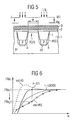
- Figures 4A to 4C show simplified sectional views for Illustration of essential manufacturing steps native field effect transistor according to a second embodiment.
- the same reference numerals designate the same or similar layers or elements, which is why below a detailed description is dispensed with.
- FIG. 4A a p - - well 1 'for a native field effect transistor is formed in an n - semiconductor substrate 1, for example by implantation.
- a detailed description for the production of such insulation areas and / or well areas is dispensed with, since they are generally known to the person skilled in the art.
- the complementary channel stop areas KKS and the normal channel stop areas KS are n-conducting in this case, but act differently on the field effect transistors formed below, since their channel areas are of the same line type or of a different line type.
- an insulating layer becomes in subsequent steps 2 thermally, for example, as a silicon dioxide layer formed and one of polysilicon or metallic Material existing control layer 3 for example deposited using a chemical vapor deposition process.
- a respective source-drain doping where for the native field effect transistor NT n-doped source and drain regions for creating an n-type channel region K are formed while for the conventional Field effect transistor T a p-doping to produce p-doped Source and drain areas and one of them p-channel range takes place.
- the channel stop doping in the native field effect transistor has the same doping or the same conductivity type is like the channel area K, one speaks of one complementary channel stop area KKS.
- the Channel stop doping for the conventional field effect transistor T opposite to the conduction type p of the channel area K, which is why this is conventional channel stop areas KS is.
- the effect of these channel stop areas is different.
- the channel stop area KS in the field effect transistor T only reduced the channel width effects and enables a reliable limitation of the channel area K, is complemented by the complementary channel stop areas KKS in the native field effect transistor NT the threshold voltage to lowered to near 0 volts.
- the threshold voltage in the native field effect transistor if in particular the complementary channel stop areas KKS for example by means of temperature-related diffusion can be introduced to the channel area K.
- An alike out-diffusion taking place in the conventional transistors T. is here for the channel stop areas KS and the properties insignificant in the channel area K if the mask for the channel stop area KS is a sufficient distance from the channel K of the transistor T.
- the distance of a channel stop area KS is therefore preferably larger than that of a complementary one KKS channel stop area selected.
- Figure 5 shows a simplified sectional view of a native Field effect transistor according to a third embodiment, the same reference numerals again being the same or similar Designate layers or elements and repeat them Description is omitted below.
- channel stop areas and complementary Channel stop areas can also use other methods such as the molecular beam epitaxy to form these areas be used.
- the respective Standard processes existing process steps optimally use for forming the complementary channel stop areas.
- FIG. 6 shows a simplified illustration of a threshold voltage V th as a function of a respective channel width w of the field effect transistor, the influences of a channel stop area KS, a complementary channel stop area KKS, an STI isolation and a LOCOS isolation being shown. Accordingly, according to the present invention, when using STI trench isolation and a complementary channel stop region KKS, a threshold voltage V th1 can be reduced to the amount V th2 , which results in the desired and often necessary native field effect transistors. According to FIG. 6, it can also be seen that, in particular in the case of field effect transistors with a small channel width w in which channel width effects occur, a particularly great effect can be achieved by the complementary channel stop regions.
- the present invention was based on specially doped p-areas or tubs described. However, it includes in equally oppositely doped areas or wells as well as further combinations of the exemplary embodiments described above. Furthermore, the present invention has been accomplished described a MOS field effect transistor. However, it is not limited to this, but includes the same Wise semiconductor devices with field effect transistor structures such as. EEPROMS, FLASH memory cells etc. In the same In this way, the isolation areas can also be formed into one other, especially later.
Landscapes
- Metal-Oxide And Bipolar Metal-Oxide Semiconductor Integrated Circuits (AREA)
Abstract
Description
Claims (14)
- Nativer Feldeffekttransistor mit
Isolationsgebieten (I) zum Ausbilden von aktiven Bereichen (AA) in einem Substrat (1) und zum Festlegen einer Kanalweite (w) eines Kanalbereichs (K);
Source- und Draingebieten (S, D) von einem ersten Leitungstyp, die zum Festlegen einer Kanallänge (1) des Kanalbereichs (K) im aktiven Bereich (AA) ausgebildet sind;
einer Isolierschicht (2), die zumindest über dem Kanalbereich (K) ausgebildet ist; und
einer Steuerschicht (3) zum Ansteuern des nativen Feldeffekttransistors (NT), gekennzeichnet durch einen komplementären Kanalstoppbereich (KKS), der im Wesentlichen unterhalb der Isolationsgebiete (I) im Substrat 1 ausgebildet ist und eine Dotierung vom ersten Leitungstyp aufweist. - Nativer Feldeffekttransistor nach Patentanspruch 1,
dadurch gekennzeichnet, dass der komplementäre Kanalstoppbereich (KKS) sich bis in den Kanalbereich (K) erstreckt. - Nativer Feldeffekttransistor nach Patentanspruch 1 oder 2,
gekennzeichnet durch einen Kanalstoppbereich (KS), der im Wesentlichen unterhalb der Isolationsgebiete (I) im Substrat 1 ausgebildet ist und eine Dotierung von zum ersten Leitungstyp entgegengesetzten zweiten Leitungstyp aufweist. - Nativer Feldeffekttransistor nach einem der Patentansprüche 1 bis 3,
dadurch gekennzeichnet, dass er in einer Wanne (1') vom zweiten Leitungstyp ausgebildet ist. - Nativer Feldeffekttransistor nach einem der Patentansprüche 1 bis 4,
dadurch gekennzeichnet, dass die Kanalweite (w) des nativen Feldeffekttransistors (NT) eine Größe aufweist, bei der Kanalweiteneffekte auftreten. - Verfahren zur Herstellung eines nativen Feldeffekttransistors (NT) mit den Schritten:a) Ausbilden von Isolationsgebieten (I) in einem Substrat (1) zum Erzeugen von aktiven Bereichen (AA) und zum Festlegen einer Kanalweite (w) eines Kanalbereichs (K);b) Ausbilden von komplementären Kanalstoppbereichen (KKS) von einem ersten Leitungstyp unterhalb der Isolationsgebiete (I) im Substrat (1);c) Ausbilden einer Isolierschicht (2) an zumindest der Oberfläche der aktiven Bereiche (AA);d) Ausbilden einer Steuerschicht (3) an zumindest der Oberfläche der Isolierschicht (2);e) Strukturieren der Steuerschicht (3) und der Isolierschicht (2) zum Ausbilden von Gatestapeln (6);f) Ausbilden von Source- und Draingebieten (S, D) vom ersten Leitungstyp zum Festlegen einer Kanallänge (1) des Kanalbereichs (K) im aktiven Bereich (AA); undg) Ausbilden von Kontakten (KT) zum Anschließen der Sourceund Draingebiete (S, D).
- Verfahren nach Patentanspruch 6,
dadurch gekennzeichnet, dass in Schritt a) STI und/oder LOCOS-Isolationsgebiete (I) ausgebildet werden. - Verfahren nach Patentanspruch 6 oder 7,
gekennzeichnet durch den weiteren Schritt b1) Ausbilden von Kanalstoppbereichen (KS) von einem zweiten zum ersten Leitungstyp entgegengesetzten Leitungstyp unterhalb der Isolätionsgebiete (I) im Substrat (1). - Verfahren nach einem der Patentansprüche 6 bis 8,
dadurch gekennzeichnet, dass die Kanalstoppbereiche (KS) und/oder die komplementären Kanalstoppbereiche (KKS) mittels Implantation (I, Ik) unter Verwendung von Kanalstopp-Masken (M, Mk) ausgebildet werden. - Verfahren nach einem der Patentansprüche 6 bis 8,
dadurch gekennzeichnet, dass die Kanalstoppbereiche (KS) und/oder die komplementären Kanalstoppbereiche (KKS) mittels Molekularstrahlepitaxie im Substrat (1) ausgebildet werden. - Verfahren nach einem der Patentansprüche 6 bis 10,
dadurch gekennzeichnet, dass in Schritt b) die komplementären Kanalstoppbereiche (KKS) mittels Diffusion bis an den Kanalbereich (K) herangeführt werden. - Verfahren nach einem der Patentansprüche 6 bis 11,
dadurch gekennzeichnet, dass in Schritt c) eine SiO2-Schicht thermisch ausgebildet wird. - Verfahren nach einem der Patentansprüche 6 bis 12,
dadurch gekennzeichnet, dass in Schritt f) die Source- und Draingebiete (S, D) mittels einer Implantation unter Verwendung des Gatestapels (G) als Maske selbstjustierend ausgebildet werden. - Verfahren nach einem der Patentansprüche 6 bis 13,
dadurch gekennzeichnet, dass die Kanalweite (w) des nativen Feldeffekttransistors (NT) eine Größe aufweist, bei der Kanalweiteneffekte auftreten.
Applications Claiming Priority (2)
| Application Number | Priority Date | Filing Date | Title |
|---|---|---|---|
| DE10108923 | 2001-02-23 | ||
| DE10108923A DE10108923C1 (de) | 2001-02-23 | 2001-02-23 | Nativer Feldeffekttransistor und Verfahren zu dessen Herstellung |
Publications (2)
| Publication Number | Publication Date |
|---|---|
| EP1235271A2 true EP1235271A2 (de) | 2002-08-28 |
| EP1235271A3 EP1235271A3 (de) | 2005-03-09 |
Family
ID=7675350
Family Applications (1)
| Application Number | Title | Priority Date | Filing Date |
|---|---|---|---|
| EP02003678A Withdrawn EP1235271A3 (de) | 2001-02-23 | 2002-02-18 | Nativer Feldeffekttransistor und Verfahren zu dessen Herstellung |
Country Status (2)
| Country | Link |
|---|---|
| EP (1) | EP1235271A3 (de) |
| DE (1) | DE10108923C1 (de) |
Cited By (1)
| Publication number | Priority date | Publication date | Assignee | Title |
|---|---|---|---|---|
| US8016374B2 (en) | 2005-11-10 | 2011-09-13 | Grass Gmbh | Pull-out slide for drawers and drawer |
Family Cites Families (7)
| Publication number | Priority date | Publication date | Assignee | Title |
|---|---|---|---|---|
| JPS62204574A (ja) * | 1986-03-05 | 1987-09-09 | Toshiba Corp | 絶縁ゲ−ト型電界効果半導体装置 |
| US5396096A (en) * | 1992-10-07 | 1995-03-07 | Matsushita Electric Industrial Co., Ltd. | Semiconductor device and manufacturing method thereof |
| US5240874A (en) * | 1992-10-20 | 1993-08-31 | Micron Semiconductor, Inc. | Semiconductor wafer processing method of forming channel stops and method of forming SRAM circuitry |
| CN1052341C (zh) * | 1993-03-26 | 2000-05-10 | 松下电器产业株式会社 | 半导体器件及其制造方法 |
| DE69732293D1 (de) * | 1997-08-27 | 2005-02-24 | St Microelectronics Srl | Herstellungsverfahren eines nativen MOS-P-Kanal-Transistors mit Verfahren für nichtflüchtige Speicher |
| US5960276A (en) * | 1998-09-28 | 1999-09-28 | Taiwan Semiconductor Manufacturing Company, Ltd. | Using an extra boron implant to improve the NMOS reverse narrow width effect in shallow trench isolation process |
| EP1003222A1 (de) * | 1998-11-19 | 2000-05-24 | STMicroelectronics S.r.l. | Verbesserter Feldeffekttransistor und Verfahren zu dessen Herstellung |
-
2001
- 2001-02-23 DE DE10108923A patent/DE10108923C1/de not_active Expired - Fee Related
-
2002
- 2002-02-18 EP EP02003678A patent/EP1235271A3/de not_active Withdrawn
Cited By (1)
| Publication number | Priority date | Publication date | Assignee | Title |
|---|---|---|---|---|
| US8016374B2 (en) | 2005-11-10 | 2011-09-13 | Grass Gmbh | Pull-out slide for drawers and drawer |
Also Published As
| Publication number | Publication date |
|---|---|
| EP1235271A3 (de) | 2005-03-09 |
| DE10108923C1 (de) | 2002-08-08 |
Similar Documents
| Publication | Publication Date | Title |
|---|---|---|
| DE4212829C2 (de) | Verfahren zur Herstellung von Metall-Oxid-Halbleiter-Feldeffekttransistoren | |
| DE4233236C2 (de) | Halbleitereinrichtung mit einem Wannenbereich für einen MOS-Transistor und Herstellungsverfahren dafür | |
| DE4219319B4 (de) | MOS-FET und Herstellungsverfahren dafür | |
| DE10214066B4 (de) | Halbleiterbauelement mit retrogradem Dotierprofil in einem Kanalgebiet und Verfahren zur Herstellung desselben | |
| DE69710609T2 (de) | Herstellungsverfahern eines integrierten schaltkreises mit unterschiedlicher gateoxidedicke | |
| DE19642538A1 (de) | Halbleitereinrichtung und Herstellungsverfahren derselben | |
| DE19744687A1 (de) | Feldeffekttransistor und Herstellungsverfahren desselben | |
| DE2707652A1 (de) | Verfahren zur bildung von kanalsperren entgegengesetzter leitungstypen im zwischenbereich zwischen zwei mos-bauelementen zugeordneten zonen eines siliziumsubstrats | |
| DE3932621A1 (de) | Halbleitervorrichtung und verfahren zur herstellung derselben | |
| DE102004062862A1 (de) | Transistor einer Halbleitervorrichtung und Verfahren zur Herstellung desselben | |
| EP1517361A2 (de) | Verfahren zur Herstellung eines MOS-Transistors mit einer Driftregion, die einen Graben aufweist | |
| DE112010004330T5 (de) | Asymmetrische Epitaxie und Anwendung derselben | |
| DE4116690A1 (de) | Elementisolationsaufbau einer halbleitereinrichtung und verfahren zur herstellung derselben | |
| DE60028847T2 (de) | Verfahren mit reduzierter Maskenzahl für die Herstellung von Mischsspannung-CMOS mit Hochleistung-Transistoren und -I/O Transistoren von hoher Zuverlässigkeit | |
| DE68928396T2 (de) | CMOS-integrierte Schaltung mit modifizierter Isolation | |
| DE102008011932A1 (de) | Verfahren zur Erhöhung der Eindringtiefe von Drain- und Sourceimplantationssorten für eine gegebene Gatehöhe | |
| DE4341516C2 (de) | Verfahren zum Herstellen eines Transistors | |
| DE60132129T2 (de) | Halbleiterbauelement mit LDD-Struktur und dessen Herstellungsverfahren | |
| WO2006037526A2 (de) | Lateraler dmos-transistor und verfahren zu seiner herstellung | |
| DE19908809A1 (de) | Verfahren zur Herstellung einer MOS-Transistorstruktur mit erhöhter Bodyleitfähigkeit | |
| DE60209065T2 (de) | Verfahren zur Herstellung einer Halbleitervorrichtung | |
| DE10138648A1 (de) | Verfahren zum parallelen Herstellen eines MOS-Transistors und eines Bipolartransistors | |
| DE102004063144A1 (de) | Halbleiter-Bauelement und Herstellungsverfahren dafür | |
| DE19821999A1 (de) | SOI-Halbleiteranordnung und Verfahren zur Herstellung derselben | |
| DE10261145A1 (de) | Verbesserter Transistor mit abgesenktem Gate und ein Verfahren zur Herstellung desselben |
Legal Events
| Date | Code | Title | Description |
|---|---|---|---|
| PUAI | Public reference made under article 153(3) epc to a published international application that has entered the european phase |
Free format text: ORIGINAL CODE: 0009012 |
|
| AK | Designated contracting states |
Kind code of ref document: A2 Designated state(s): AT BE CH CY DE DK ES FI FR GB GR IE IT LI LU MC NL PT SE TR |
|
| AX | Request for extension of the european patent |
Free format text: AL;LT;LV;MK;RO;SI |
|
| PUAL | Search report despatched |
Free format text: ORIGINAL CODE: 0009013 |
|
| AK | Designated contracting states |
Kind code of ref document: A3 Designated state(s): AT BE CH CY DE DK ES FI FR GB GR IE IT LI LU MC NL PT SE TR |
|
| AX | Request for extension of the european patent |
Extension state: AL LT LV MK RO SI |
|
| 17P | Request for examination filed |
Effective date: 20050304 |
|
| AKX | Designation fees paid |
Designated state(s): DE FR GB |
|
| 17Q | First examination report despatched |
Effective date: 20060405 |
|
| 17Q | First examination report despatched |
Effective date: 20060405 |
|
| STAA | Information on the status of an ep patent application or granted ep patent |
Free format text: STATUS: THE APPLICATION IS DEEMED TO BE WITHDRAWN |
|
| 18D | Application deemed to be withdrawn |
Effective date: 20080220 |