EP1225670B1 - Dispositif semi-conducteur avec structure à confinement de courant - Google Patents
Dispositif semi-conducteur avec structure à confinement de courant Download PDFInfo
- Publication number
- EP1225670B1 EP1225670B1 EP01300447A EP01300447A EP1225670B1 EP 1225670 B1 EP1225670 B1 EP 1225670B1 EP 01300447 A EP01300447 A EP 01300447A EP 01300447 A EP01300447 A EP 01300447A EP 1225670 B1 EP1225670 B1 EP 1225670B1
- Authority
- EP
- European Patent Office
- Prior art keywords
- current
- blocking structure
- active layer
- current blocking
- conduction region
- Prior art date
- Legal status (The legal status is an assumption and is not a legal conclusion. Google has not performed a legal analysis and makes no representation as to the accuracy of the status listed.)
- Expired - Lifetime
Links
Images


Classifications
-
- H—ELECTRICITY
- H01—ELECTRIC ELEMENTS
- H01L—SEMICONDUCTOR DEVICES NOT COVERED BY CLASS H10
- H01L33/00—Semiconductor devices with at least one potential-jump barrier or surface barrier specially adapted for light emission; Processes or apparatus specially adapted for the manufacture or treatment thereof or of parts thereof; Details thereof
- H01L33/02—Semiconductor devices with at least one potential-jump barrier or surface barrier specially adapted for light emission; Processes or apparatus specially adapted for the manufacture or treatment thereof or of parts thereof; Details thereof characterised by the semiconductor bodies
- H01L33/14—Semiconductor devices with at least one potential-jump barrier or surface barrier specially adapted for light emission; Processes or apparatus specially adapted for the manufacture or treatment thereof or of parts thereof; Details thereof characterised by the semiconductor bodies with a carrier transport control structure, e.g. highly-doped semiconductor layer or current-blocking structure
- H01L33/145—Semiconductor devices with at least one potential-jump barrier or surface barrier specially adapted for light emission; Processes or apparatus specially adapted for the manufacture or treatment thereof or of parts thereof; Details thereof characterised by the semiconductor bodies with a carrier transport control structure, e.g. highly-doped semiconductor layer or current-blocking structure with a current-blocking structure
-
- B—PERFORMING OPERATIONS; TRANSPORTING
- B82—NANOTECHNOLOGY
- B82Y—SPECIFIC USES OR APPLICATIONS OF NANOSTRUCTURES; MEASUREMENT OR ANALYSIS OF NANOSTRUCTURES; MANUFACTURE OR TREATMENT OF NANOSTRUCTURES
- B82Y20/00—Nanooptics, e.g. quantum optics or photonic crystals
-
- H—ELECTRICITY
- H01—ELECTRIC ELEMENTS
- H01S—DEVICES USING THE PROCESS OF LIGHT AMPLIFICATION BY STIMULATED EMISSION OF RADIATION [LASER] TO AMPLIFY OR GENERATE LIGHT; DEVICES USING STIMULATED EMISSION OF ELECTROMAGNETIC RADIATION IN WAVE RANGES OTHER THAN OPTICAL
- H01S5/00—Semiconductor lasers
- H01S5/10—Construction or shape of the optical resonator, e.g. extended or external cavity, coupled cavities, bent-guide, varying width, thickness or composition of the active region
- H01S5/12—Construction or shape of the optical resonator, e.g. extended or external cavity, coupled cavities, bent-guide, varying width, thickness or composition of the active region the resonator having a periodic structure, e.g. in distributed feedback [DFB] lasers
-
- H—ELECTRICITY
- H01—ELECTRIC ELEMENTS
- H01S—DEVICES USING THE PROCESS OF LIGHT AMPLIFICATION BY STIMULATED EMISSION OF RADIATION [LASER] TO AMPLIFY OR GENERATE LIGHT; DEVICES USING STIMULATED EMISSION OF ELECTROMAGNETIC RADIATION IN WAVE RANGES OTHER THAN OPTICAL
- H01S5/00—Semiconductor lasers
- H01S5/20—Structure or shape of the semiconductor body to guide the optical wave ; Confining structures perpendicular to the optical axis, e.g. index or gain guiding, stripe geometry, broad area lasers, gain tailoring, transverse or lateral reflectors, special cladding structures, MQW barrier reflection layers
- H01S5/22—Structure or shape of the semiconductor body to guide the optical wave ; Confining structures perpendicular to the optical axis, e.g. index or gain guiding, stripe geometry, broad area lasers, gain tailoring, transverse or lateral reflectors, special cladding structures, MQW barrier reflection layers having a ridge or stripe structure
- H01S5/2205—Structure or shape of the semiconductor body to guide the optical wave ; Confining structures perpendicular to the optical axis, e.g. index or gain guiding, stripe geometry, broad area lasers, gain tailoring, transverse or lateral reflectors, special cladding structures, MQW barrier reflection layers having a ridge or stripe structure comprising special burying or current confinement layers
- H01S5/2222—Structure or shape of the semiconductor body to guide the optical wave ; Confining structures perpendicular to the optical axis, e.g. index or gain guiding, stripe geometry, broad area lasers, gain tailoring, transverse or lateral reflectors, special cladding structures, MQW barrier reflection layers having a ridge or stripe structure comprising special burying or current confinement layers having special electric properties
- H01S5/2226—Structure or shape of the semiconductor body to guide the optical wave ; Confining structures perpendicular to the optical axis, e.g. index or gain guiding, stripe geometry, broad area lasers, gain tailoring, transverse or lateral reflectors, special cladding structures, MQW barrier reflection layers having a ridge or stripe structure comprising special burying or current confinement layers having special electric properties semiconductors with a specific doping
-
- H—ELECTRICITY
- H01—ELECTRIC ELEMENTS
- H01S—DEVICES USING THE PROCESS OF LIGHT AMPLIFICATION BY STIMULATED EMISSION OF RADIATION [LASER] TO AMPLIFY OR GENERATE LIGHT; DEVICES USING STIMULATED EMISSION OF ELECTROMAGNETIC RADIATION IN WAVE RANGES OTHER THAN OPTICAL
- H01S5/00—Semiconductor lasers
- H01S5/20—Structure or shape of the semiconductor body to guide the optical wave ; Confining structures perpendicular to the optical axis, e.g. index or gain guiding, stripe geometry, broad area lasers, gain tailoring, transverse or lateral reflectors, special cladding structures, MQW barrier reflection layers
- H01S5/22—Structure or shape of the semiconductor body to guide the optical wave ; Confining structures perpendicular to the optical axis, e.g. index or gain guiding, stripe geometry, broad area lasers, gain tailoring, transverse or lateral reflectors, special cladding structures, MQW barrier reflection layers having a ridge or stripe structure
- H01S5/227—Buried mesa structure ; Striped active layer
- H01S5/2275—Buried mesa structure ; Striped active layer mesa created by etching
-
- H—ELECTRICITY
- H01—ELECTRIC ELEMENTS
- H01S—DEVICES USING THE PROCESS OF LIGHT AMPLIFICATION BY STIMULATED EMISSION OF RADIATION [LASER] TO AMPLIFY OR GENERATE LIGHT; DEVICES USING STIMULATED EMISSION OF ELECTROMAGNETIC RADIATION IN WAVE RANGES OTHER THAN OPTICAL
- H01S5/00—Semiconductor lasers
- H01S5/30—Structure or shape of the active region; Materials used for the active region
- H01S5/34—Structure or shape of the active region; Materials used for the active region comprising quantum well or superlattice structures, e.g. single quantum well [SQW] lasers, multiple quantum well [MQW] lasers or graded index separate confinement heterostructure [GRINSCH] lasers
- H01S5/343—Structure or shape of the active region; Materials used for the active region comprising quantum well or superlattice structures, e.g. single quantum well [SQW] lasers, multiple quantum well [MQW] lasers or graded index separate confinement heterostructure [GRINSCH] lasers in AIIIBV compounds, e.g. AlGaAs-laser, InP-based laser
- H01S5/3434—Structure or shape of the active region; Materials used for the active region comprising quantum well or superlattice structures, e.g. single quantum well [SQW] lasers, multiple quantum well [MQW] lasers or graded index separate confinement heterostructure [GRINSCH] lasers in AIIIBV compounds, e.g. AlGaAs-laser, InP-based laser with a well layer comprising at least both As and P as V-compounds
Definitions
- the present invention relates to a semiconductor device with one or more current confinement regions and to a method of manufacturing such a device, particularly buried heterostructure light emitting devices such as semiconductor lasers and light emitting diodes.
- Buried heterostructure light emitting devices commonly have current confinement regions defined by areas of high resistivity that channel current to an optically active layer within the structure.
- current confinement regions have been employed based on a reverse-biased p-n or n-p diode structure.
- Such structures provide high resistivity, and low leakage currents, and are widely used in fibre optic communication systems across a range of operating frequencies. At operating frequencies about 1 GHz, however, the performance of such devices becomes limited by the capacitance of the current blocking structure, owing to the charge on the reverse biased diode junction.
- Fe-doped InP-based layers have a lower capacitance than structures based on a reverse biased junction, but do not have as high a resistivity. This lower resistivity also limits operation and device lifetime at high frequencies, because of the resulting higher device operating temperatures. In order to avoid excessive temperatures, it becomes necessary to use a lower drive voltage, and this in turn limits the achievable bandwidth of a device based on Fe-doped material.
- EP-A-0 547 850 and US-A-5 636 237 both disclose a semiconductor laser device comprising an active layer and a mesa-stripe shaped current conduction region, with a current confinement region located on either side of the current conduction region, the current conduction region and current confinement region being arranged to channel electric current to the active layer, wherein each current confinement region includes both a metal-doped current blocking structure (Fe doped InP) and a p-n junction current blocking structure, the p-n current blocking structure being grown adjacent the active layer, between the current conduction region and the metal-doped current blocking structure.
- a metal-doped current blocking structure Fe doped InP
- p-n current blocking structure being grown adjacent the active layer, between the current conduction region and the metal-doped current blocking structure.
- the layers of the p-n junction current blocking structure are etched with a photolithography technique, which cuts curved side walls through these layers, and the metal doped current blocking structure is subsequently grown adjacent to these curved side walls of the p-n junction current blocking structure.
- the p-n junction current blocking structure is deposited with curved side walls, and the metal doped current blocking structure is subsequently grown adjacent to the outermost curved side wall of the p-n junction current blocking structure.
- fibre optic communication links having a bandwidth in excess of 1 GHz, for example up to 10 GHz. It is an object of the present invention to provide a semiconductor device that addresses these issues.
- the invention provides a semiconductor device comprising an active layer, a current conduction region, one or more current confinement regions adjacent the current conduction region, the current conduction region and current confinement region being arranged to channel electric current to the active layer, wherein the or each current confinement region includes both a metal-doped current blocking structure and a p-n junction current blocking structure, the p-n current blocking structure being between the current conduction region and the metal-doped current blocking structure and wherein the metal-doped current blocking structure abuts the p-n current blocking structure along a substantially vertical interface.
- the p-n current blocking structure nearest the current conduction region then provides high resistivity and good high frequency performance at high temperatures, while the reduction in the volume of the p-n current blocking structure and use of the metal-doped second current blocking structure further away from the current conduction region provides reduced parasitic capacitance.
- the device in some types of device, for example buried heterostructure laser diodes, the device includes a substrate, a mesa stripe on the substrate and the active layer in the mesa stripe.
- the current conduction region then channels current through the active layer.
- the mesa stripe may have side walls that rise above the substrate.
- the active layer then extends to the side walls and the active layer is covered at the side walls by the p-n blocking structure.
- the mesa side walls slope laterally away from the active layer towards the metal-doped current blocking structure.
- a method of forming a semiconductor device comprising an active layer, a current conduction region, one or more current confinement regions adjacent the current conduction region, the current conduction region and current confinement region being arranged to channel electric current to the active layer, wherein the method comprises the steps of:
- a first etch mask is formed over the active layer, said first etch mask defining during a first etching process an area of the active layer adjacent the current conduction region to be removed by the etching.
- a second etch mask is formed over the active layer and the p-n junction current blocking structure adjacent the current conduction region, said second etch mask defining during the reactive ion plasma dry etch process an area of p-n junction current blocking structure not adjacent the active layer to be removed by the etching.
- This second etch mask may then remain in place during the growth of the metal-doped current blocking structure in step iii).
- the second etch mask is then aligned laterally with the first etch mask, typically to an accuracy of about 10% to 20% of the width of the second etch mask. In one preferred embodiment of the invention, the second etch mask is laterally wider than the first etch mask.
- an etch mask is formed over the active layer, said etch mask defining during a first etching process an area of the active layer adjacent the current conduction region to be removed by the etching.
- the etch mask remains during the growth of the p-n current blocking structure in step ii).
- the etch mask also defines during the reactive ion plasma dry etch process an area of the p-n junction current blocking structure not adjacent the active layer to be removed by the etching.
- This etch mask may then remain in place during the growth of the metal-doped current blocking structure in step iii).
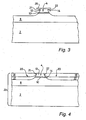
- Figure 1 shows, not to scale, a cross-section of a semiconductor device 1 according to the invention, here a buried heterostructure laser diode suitable for use as a transmitter in a high speed fibre-optic link operating at 1.55 ⁇ m.
- high speed links operate at 2.5 or 10 Gbits/s, and bit rates of up to 40 Gbits/s have been demonstrated in the laboratory.
- the device 1 is formed starting from a wafer 3 that is 32 mm square, and that has an n -- -InP substrate 2 doped to around 10 19 /cc, on which is grown a 2 ⁇ m thick n - -InP buffer layer 8 doped to around 10 18 /cc.
- An active layer 10 is grown on the buffer layer 8 according to known techniques for fabricating planar active lasers for a laser diode - the active layer could be a bulk region or a strained multiple quantum well (SMQW) structure.
- SMQW strained multiple quantum well
- An example of an SMQW device is discussed in W. S. Ring et al, Optical Fibre Conference, Vol. 2, 1996 Technical Digest Series, Optical Society of America .
- the type of active layer employed is not critical to the invention.
- the laser diode 1 has a quaternary In x Ga 1-x As 1-y P y active layer 10 that may be between about 100 nm to 300 nm thick.
- the active layer 10 is topped by another buffer layer 12, also called a P 0 -layer, formed from p + -InP, grown to be between about 400 nm to 1 ⁇ m thick.
- a DFB grating for the laser diode 1 can be contained in the n - -InP buffer layer 8 or in an additional p-InGaAsP grating layer.
- the wafer 3 is coated with an oxide layer 16 as shown in Figure 2 .
- the oxide layer may be SiO 2 deposited by a plasma enhanced chemical vapour deposition (PECVD) process. It should, however, be noted that silicon nitride would be a suitable alternative choice to SiO 2 .
- the oxide layer 16 is photolithographicly patterned with a photoresist to leave a patterned mask 26, and etched to remove in areas not covered by the patterned mask the P 0 -layer 12, the active layer 10, and all but 200 nm of the buffer layer 8.
- layers 8, 10 and 12 are removed in a wet-etch process that undercuts the patterned mask 26 by about 200 nm to 500 nm.
- the layers 8, 10, and 12 are removed in all areas except along a mesa stripe 14 structure that extends perpendicular to the plane of the drawing, and which rises above the level of the substrate 2.
- the mesa stripe 14 has left and right opposite side walls 21,22 that together with the buffer layer 8 and the P 0 -layer 12 form a current conduction region 4 for an applied current I, and have the effect of guiding an optical mode 15 along the active layer 10 within the stripe 14.
- the width of the mesa stripe 14 varies depending on the particular device, but for opto-electronic devices such as laser diodes, the ridge stripe 14 is usually between 1 ⁇ m and 10 ⁇ m wide. The ridge strip 14 rises 1 ⁇ m to 2 ⁇ m above the surrounding substrate 2.
- a first current blocking structure 20 is then grown on the etched device up to approximately the level of the patterned mask 26, first with a p-doped InP layer 17, and then with an n-doped InP layer 18.
- the thicknesses of the p-doped and n-doped layers are similar. These InP layers 17,18 form a p-n junction that is insulating when the laser diode 1 is forward biased.
- the PECVD oxide layer 16 is removed with 10:1 buffered HF from the ridge strip 14 to expose again the P 0 -layer 12. This leaves an etched and coated wafer 23 comprising the substrate 2, the mesa stripe 14 and the first current blocking structure 20 abutting the opposite sides 21,22 of the mesa stripe 14.
- the etched and coated wafer 23 is coated with an oxide layer, such as an SiO 2 layer or silicon nitride layer deposited by PECVD, which is then pholithographicly patterned and etched as described above to leave a second patterned mask 36.
- the second patterned mask 36 is aligned along the length of the mesa stripe 14, but is wider than the mesa stripe, so that the mask 36 and extends at least 1 ⁇ m and preferably 2 ⁇ m laterally beyond the junction between each mesa side 21,22 and a top surface 37 of the P 0 -layer 12.
- the P 0 -layer 12, the active layer 10, and preferably all of the buffer layer 8 are then removed in a reactive ion plasma dry etch process, which cuts substantially vertical sides walls 41,42 through these layers.
- the resulting etched structure 44 is shown in Figure 5 .
- a second current blocking structure 45 is then grown using a MOVCD process on the exposed semiconductor surfaces of the etched structure 44.
- This current blocking structure is formed from a Fe-doped InP-based layer 46 topped by an n - -InP layer 47.
- the metal dopant could be ruthenium or chromium.
- the thickness of the Fe-InP layer is about 1 ⁇ m to 2 ⁇ m, so that this extends almost up to the mask 36.
- the n - -InP layer is about 200 nm to 500 nm thick, and extends just above the mask 36.
- the second current blocking structure 45 therefore abuts the side walls 41,42 of the first current blocking structure 20 along a substantially vertical interface, and the first current blocking structure 20 abuts the side walls 21,22 of the mesa stripe 14. Because the second current blocking structure 45 extends deeper within the current blocking region than the first current blocking structure 20, the second current blocking structure 45 also abuts a portion of the n - -InP buffer layer 8 along a substantially vertical interface.
- n - -InP layer 47 in the second blocking structure 45 blocks the conduction of holes through the blocking structure as well as acting as a barrier to the diffusion of Zn into the metal-doped layer 46.
- the patterned oxide layer 36 is removed with 10:1 buffered HF from the ridge strip 14 to expose again the P 0 -layer 12.
- a cladding layer 48 formed from p + -InP is then grown above the P 0 -layer 12 and current blocking structures 20,45 to a thickness of about 2 ⁇ m to 3 ⁇ m.
- the final semiconductor layer is a 100 nm to 200 nm thick ternary cap layer 49 deposited on the cladding layer 48.
- the cap layer 49 is formed from p ++ -GaInAs, highly doped to around 10 19 /cc, in order to provide a good low resistance ohmic contact for electrical connection to the current conduction region 4 of the mesa stripe 14.
- a ternary cap layer it is possible to use a quaternary InGaAsP cap layer.
- Metal 50 is then vacuum deposited on the cap layer 49 using well known techniques in two stages, first with a TiPt layer that is patterned using a lift-off process, and then final depositing of a TiAu layer, followed by metal wet etch in a photolithographically defined area. The remaining TiAu layer forms a contact pad 52 with good ohmic contact through the cap layer 49.
- the resulting wafer 54 is then thinned to a thickness of about 70 ⁇ m to 100 ⁇ m in a standard way, in order to assist with cleaving.
- the thinned wafer is then inscribed and cleaved in a conventional process first transversely into bars about 350 ⁇ m wide, and then each bar is cleaved into individual devices 200 ⁇ m wide.
- the cleaved device 1 is about 350 ⁇ m long (i.e. in the direction of the mesa 14) and about 200 ⁇ m wide.
- a Ti/Au metal layer 53 is then deposited by sputtering on the rear surface of the wafer, so enabling the device to be soldered onto a heat sink.
- the device 1 may be packaged in an industry standard package, with a single mode optical fibre coupled with a spherical lens to an output facet of the laser diode, and with gold bond wires soldered onto the metalised contact 52.
- the InGaAs/InP device 1 described above therefore incorporates a compound current confinement region formed from a reverse-biased p-n structure nearest the active region 10, and further away from the active region 10, a metal-doped InP-based layer.
- the p-n structure nearest the active region provides superior temperature performance, compared with a purely metal-doped current confinement region, while at the same time excess leakage current through the first current confinement structure at high operating frequencies due to parasitic capacitance from the reverse-biased diode structure is reduced owing to the reduced volume or amount of such a structure. Therefore, as will be described in further detail below, the invention provides a high resistivity current confinement region, and low leakage currents, across a wide range of operating temperatures. The invention also permits the use of higher drive voltages, which are useful in achieving high-speed operation.
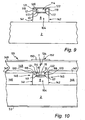
- Figures 8 to 10 show how the process described above may be modified, in a second embodiment 101 of the invention, where features corresponding with those of Figures 1 to 7 are given similar reference numerals incremented by 100.
- the process used to create the second embodiment 101 differs from that used to create the first embodiment 1 in that only one patterned inorganic mask 126 need be deposited on the wafer.
- This mask is used in the modified process in such a way that the mask 126 assures the self-alignment of the first current blocking structure 120 with respect to the second current blocking structure 145.
- the mask 126 is wider than the corresponding patterned mask shown in Figure 3 .
- the layers of the first current blocking structure 120, the p-doped InP layer 117 and n-doped InP layer 118 can still be grown up approximately to the level of the mask 126.
- the mask 126 is wide enough so that width of the first current blocking layer beneath the mask is sufficient for good highfrequency performance, as described above. Therefore, the first current blocking structure 120 and underlying buffer layer 8 outside the area of the mask 126 can be removed in a reactive ion plasma etching process, as shown in Figure 9 .
- the wafer is then processed in a similar manner to the first embodiment.
- the second current blocking structure 145 is formed with a 1 ⁇ m to 2 ⁇ m thick Fe-doped InP layer 146, overlain with a 200 nm to 500 nm thick n - -InP layer up to about the level of the top of the mesa strip 114.
- the mask 126 is then removed, followed by formation of the cladding layer 148, cap layer 149, metallic contact layer 150, and formation of a contacts 152,53 above the mesa stripe 114 and the substrate 2.
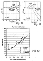
- FIG. 11 to 13 The performance of a semiconductor laser diode according to the invention is shown in Figures 11 to 13 .
- the small signal response against operating frequency at respectively 25°C and 85°C is shown respectively in Figures 11 and 12 , as a plot of the small signal initial slope S21 in dBo (dB optical) against operating frequency in GHz.
- the small signal drop off crosses -3 dB near 15 GHz.
- the signal fall time (90% to 10%) was measured to be about 85 ps. This is much better than the signal fall time of a standard buried heterostructure laser diode device with only a p-n junction current blocking layer either side of the mesa stripe, which is typically between 120 ps to 250 ps.
- Figure 13 shows a plot of fall time for the laser device of Figure 1 , within the circle labelled with reference numeral 70, compared against a range of other types of semiconductor laser devices. As can be seen, the typical fall time and S21 initial slope characteristics are very good.
- Semiconductor devices according to the invention provide a high operating bandwidth and good lifetime characteristics.
- the process steps involved may be similar to other standard steps used in the fabrication of such devices. There is no need for additional expensive processing equipment.
- the tolerances in the alignment of the mask or masks used to form the two current confinement structures are not unduly difficult to achieve using standard processing equipment.
- the present invention has been described specifically for the example of a laser diode, the invention is applicable to any high speed semiconductor device where current blocking regions help to channel current through a current conduction region, for example ridge waveguide type lasers, pump lasers, edge emitting light emitting diodes, edge photodetectors, surface emitting laser and light emitting diodes, and top-entry photodetectors.
- Another example is an optical waveguide with a split into two waveguides at a Y-junction. This may have electrically driven or modulated active optical regions in two or three of the arms of the "Y", for example an optical amplifier or modulator. It may then be desirable to provide a current blocking region at the junction of the three arms, where there may be three separate conduction regions.
- the invention described above have been described for a device based on an n -- -InP substrate, and having a first current blocking structure formed from a reverse biased p-n junction in laterally adjacent contact with the active layer structure, and a second current blocking structure formed from a metal-doped/n - InP layer structure in laterally adjacent contact with the first current blocking structure.
- the first current blocking structure may be a reverse biased n-p junction
- the second current blocking structure may include a metal-doped/p + InP layer structure in laterally adjacent contact with the first current blocking structure.
- the term "p-n junction current blocking structure" therefore includes such a reverse biased n-p junction.
Claims (9)
- Dispositif semi-conducteur (1, 101) comprenant une couche active (10), une région (4 ; 104) de conduction de courant, une ou plusieurs régions (20, 45 ; 120, 145) de confinement de courant à proximité de la région de conduction de courant, la région (4 ; 104) de conduction de courant et la région (20, 45 ; 120, 145) de confinement de courant étant configurées pour entraîner du courant électrique vers la couche active (10), dans lequel la ou chaque région de confinement de courant comporte à la fois une structure (45 ; 145) de blocage de courant dopée au métal et une structure (20 ; 120) de blocage de courant de jonction p-n, la structure (20 ; 120) de blocage de courant p-n étant entre la région (4 ; 104) de conduction de courant et la structure (45 ; 145) de blocage de courant dopée au métal, et dans lequel la structure (45 ; 145) de blocage de courant dopée au métal vient en appui contre la structure (20, -120) de blocage de courant p-n le long d'une interface (41, 42 ; 141, 142) sensiblement verticale.
- Dispositif semi-conducteur selon la revendication 1, le dispositif comportant un substrat (2), une bande mesa (14 ; 114) sur le substrat (2) et la couche active (10) dans la bande mesa (14 ; 114), dans lequel la région (4 ; 104) de conduction de courant entraîne le courant à travers la couche active (10).
- Dispositif semi-conducteur selon la revendication 2, dans lequel la bande mesa (14 ; 114) a des parois latérales (21, 22 ; 121, 122) qui dépassent au-dessus du substrat (2), la couche active (10) s'étendant vers les parois latérales (21, 22 ; 121, 122) et la couche active (10) étant recouverte au niveau des parois latérales (21, 22 ; 121, 122) par la structure (20 ; 120) de blocage p-n.
- Dispositif semi-conducteur (1) selon la revendication 2 ou la revendication 3, dans lequel les parois latérales mesa (21, 22 ; 121, 122) s'éloignent latéralement en pente de la couche active (10) jusqu'à la structure (45 ; 145) de blocage de courant dopée au métal.
- Dispositif semi-conducteur (1) selon l'une quelconque des revendications précédentes, dans lequel le dispositif (1) est un dispositif à diode laser à structure hétérogène enfouie.
- Dispositif semi-conducteur (1) selon l'une quelconque des revendications précédentes, dans lequel le dispositif (1) est formé à partir de matériaux semiconducteurs III-V.
- Procédé pour former un dispositif semi-conducteur (1, 101) comprenant une couche active (10), une région (4 ; 104) de conduction de courant, une ou plusieurs régions (20, 45 ; 120, 145) de confinement de courant à proximité de la région de conduction de courant, la région (4, 104) de conduction de courant et la région (20, 45 ; 120, 145) de confinement de courant étant configurées pour entraîner du courant électrique vers la couche active (10), dans lequel le procédé comprend les étapes consistant à :i) faire pousser sur un substrat semi-conducteur (2) une pluralité de couches semi-conductrices, comportant une couche tampon (8), la couche active (10) et la région (4 ; 104) de conduction de courant par laquelle le courant électrique peut être appliqué à la couche active (10) ;ii) faire pousser à proximité de la couche active (10) une structure (20 ; 120) de blocage de courant de jonction p-n,iii) découper les parois latérales (41, 42) sensiblement verticales à travers les couches formées dans un procédé de gravure à sec par plasma ionique réactif, etiv) faire pousser à proximité des parois latérales sensiblement verticales de la structure (20 ; 120) de blocage de courant de jonction p-n une structure (45 ; 145) de blocage de courant dopée au métal, de sorte que la structure de blocage de courant dopée au métal vienne en appui contre la structure de blocage de courant p-n le long d'une interface sensiblement verticale, la structure de blocage de courant de jonction p-n et la structure (45 ; 145) de blocage de courant dopée au métal formant ensemble une région de confinement de courant pour entraîner du courant électrique vers la région (4 ; 104) de conduction de courant.
- Procédé selon la revendication 7, dans lequel :avant l'étape ii) un premier masque d'attaque (26) est formé au dessus de la couche active (10), ledit premier masque d'attaque (26) définissant pendant un premier procédé d'attaque une zone de la couche active à proximité de la région (4) de conduction de courant pour être retirée par l'attaque ; etavant l'étape iii) un deuxième masque d'attaque (36) est formé sur la couche active (10) et la structure (20) de blocage de courant de jonction p-n à proximité de la région (4) de conduction de courant, ledit deuxième masque d'attaque (36) définissant pendant ledit procédé de gravure à sec par plasma ionique réactif une zone de la structure (20) de blocage de courant de jonction p-n pas adjacente à la couche active (10) pour être retirée par l'attaque.
- Procédé selon la revendication 7, dans lequel :avant l'étape ii), un masque d'attaque (126) est formé sur la couche active (10), ledit masque d'attaque définissant pendant un premier procédé d'attaque une zone de la couche active à proximité de la région (104) de conduction de courant pour être retirée par l'attaque ;ledit premier masque d'attaque (126) reste pendant la formation de la structure (120) de blocage de courant p-n dans l'étape ii) ; etledit masque d'attaque (126) définit aussi pendant ledit procédé de gravure à sec par plasma réactif une zone de la structure (20) de blocage de courant de jonction p-n pas adjacente à la couche active (10) pour être retirée par l'attaque.
Priority Applications (4)
| Application Number | Priority Date | Filing Date | Title |
|---|---|---|---|
| EP01300447A EP1225670B1 (fr) | 2001-01-18 | 2001-01-18 | Dispositif semi-conducteur avec structure à confinement de courant |
| DE60136261T DE60136261D1 (de) | 2001-01-18 | 2001-01-18 | Halbleiterbauelement mit Strombegrenzungstruktur |
| US09/858,677 US6509580B2 (en) | 2001-01-18 | 2001-05-16 | Semiconductor device with current confinement structure |
| JP2002005692A JP2002232080A (ja) | 2001-01-18 | 2002-01-15 | 電流閉じ込め構造を持つ半導体素子及びその製造方法 |
Applications Claiming Priority (1)
| Application Number | Priority Date | Filing Date | Title |
|---|---|---|---|
| EP01300447A EP1225670B1 (fr) | 2001-01-18 | 2001-01-18 | Dispositif semi-conducteur avec structure à confinement de courant |
Publications (2)
| Publication Number | Publication Date |
|---|---|
| EP1225670A1 EP1225670A1 (fr) | 2002-07-24 |
| EP1225670B1 true EP1225670B1 (fr) | 2008-10-22 |
Family
ID=8181652
Family Applications (1)
| Application Number | Title | Priority Date | Filing Date |
|---|---|---|---|
| EP01300447A Expired - Lifetime EP1225670B1 (fr) | 2001-01-18 | 2001-01-18 | Dispositif semi-conducteur avec structure à confinement de courant |
Country Status (4)
| Country | Link |
|---|---|
| US (1) | US6509580B2 (fr) |
| EP (1) | EP1225670B1 (fr) |
| JP (1) | JP2002232080A (fr) |
| DE (1) | DE60136261D1 (fr) |
Cited By (1)
| Publication number | Priority date | Publication date | Assignee | Title |
|---|---|---|---|---|
| DE102010026518A1 (de) * | 2010-07-08 | 2012-01-12 | Osram Opto Semiconductors Gmbh | Leuchtdiodenchip und Verfahren zur Herstellung eines Leuchtdiodenchips |
Families Citing this family (9)
| Publication number | Priority date | Publication date | Assignee | Title |
|---|---|---|---|---|
| DE10108079A1 (de) * | 2000-05-30 | 2002-09-12 | Osram Opto Semiconductors Gmbh | Optisch gepumpte oberflächenemittierende Halbleiterlaservorrichtung und Verfahren zu deren Herstellung |
| US6829275B2 (en) | 2001-12-20 | 2004-12-07 | Bookham Technology, Plc | Hybrid confinement layers of buried heterostructure semiconductor laser |
| DE60215131T2 (de) * | 2002-06-12 | 2007-03-15 | Agilent Technologies, Inc. (n.d.Ges.d.Staates Delaware), Palo Alto | Integriertes Halbleiterlaser-Wellenleiter-Element |
| EP1372229B1 (fr) * | 2002-06-12 | 2006-02-15 | Agilent Technologies Inc., A Delaware Corporation | Element integré composé d'un laser semiconducteur et d'un guide d'ondes |
| KR100547830B1 (ko) * | 2003-08-13 | 2006-01-31 | 삼성전자주식회사 | 집적광학장치 및 그 제조방법 |
| US7009214B2 (en) | 2003-10-17 | 2006-03-07 | Atomic Energy Council —Institute of Nuclear Energy Research | Light-emitting device with a current blocking structure and method for making the same |
| JP2005260109A (ja) * | 2004-03-15 | 2005-09-22 | Fujitsu Ltd | 光半導体素子 |
| JP5803366B2 (ja) * | 2011-07-14 | 2015-11-04 | 住友電気工業株式会社 | 埋め込みヘテロ構造半導体レーザの製造方法及び埋め込みヘテロ構造半導体レーザ |
| US11133649B2 (en) * | 2019-06-21 | 2021-09-28 | Palo Alto Research Center Incorporated | Index and gain coupled distributed feedback laser |
Family Cites Families (11)
| Publication number | Priority date | Publication date | Assignee | Title |
|---|---|---|---|---|
| US4425650A (en) * | 1980-04-15 | 1984-01-10 | Nippon Electric Co., Ltd. | Buried heterostructure laser diode |
| DE69209287T2 (de) * | 1991-05-07 | 1996-11-14 | British Telecomm | Optische extraktion von taktimpulsen |
| JPH05167191A (ja) * | 1991-12-18 | 1993-07-02 | Furukawa Electric Co Ltd:The | 埋め込み型半導体レーザ素子 |
| JPH0722691A (ja) * | 1993-06-30 | 1995-01-24 | Mitsubishi Electric Corp | 半導体レーザとその製造方法 |
| EP0639875A1 (fr) * | 1993-07-12 | 1995-02-22 | BRITISH TELECOMMUNICATIONS public limited company | Structure de barrière électrique pour dispositif semiconducteur |
| JPH0851250A (ja) * | 1994-08-09 | 1996-02-20 | Mitsubishi Electric Corp | 半導体レーザ |
| US5832019A (en) * | 1994-11-28 | 1998-11-03 | Xerox Corporation | Index guided semiconductor laser biode with shallow selective IILD |
| JP3386261B2 (ja) * | 1994-12-05 | 2003-03-17 | 三菱電機株式会社 | 光半導体装置、及びその製造方法 |
| JPH08213691A (ja) * | 1995-01-31 | 1996-08-20 | Nec Corp | 半導体レーザ |
| JPH0918079A (ja) * | 1995-06-27 | 1997-01-17 | Mitsubishi Electric Corp | 半導体装置の製造方法,及び半導体装置 |
| JP3241002B2 (ja) * | 1998-09-02 | 2001-12-25 | 日本電気株式会社 | 半導体レーザの製造方法 |
-
2001
- 2001-01-18 EP EP01300447A patent/EP1225670B1/fr not_active Expired - Lifetime
- 2001-01-18 DE DE60136261T patent/DE60136261D1/de not_active Expired - Fee Related
- 2001-05-16 US US09/858,677 patent/US6509580B2/en not_active Expired - Lifetime
-
2002
- 2002-01-15 JP JP2002005692A patent/JP2002232080A/ja not_active Withdrawn
Cited By (1)
| Publication number | Priority date | Publication date | Assignee | Title |
|---|---|---|---|---|
| DE102010026518A1 (de) * | 2010-07-08 | 2012-01-12 | Osram Opto Semiconductors Gmbh | Leuchtdiodenchip und Verfahren zur Herstellung eines Leuchtdiodenchips |
Also Published As
| Publication number | Publication date |
|---|---|
| US20020093013A1 (en) | 2002-07-18 |
| DE60136261D1 (de) | 2008-12-04 |
| JP2002232080A (ja) | 2002-08-16 |
| EP1225670A1 (fr) | 2002-07-24 |
| US6509580B2 (en) | 2003-01-21 |
Similar Documents
| Publication | Publication Date | Title |
|---|---|---|
| AU651111B2 (en) | Optoelectronic device | |
| EP0437836A2 (fr) | Dispositif optique semi-conducteur | |
| US8558245B2 (en) | Optical semiconductor device having ridge structure formed on active layer containing p-type region and its manufacture method | |
| US6995454B2 (en) | Semiconductor optical integrated device having a light emitting portion, a modulation section and a separation portion | |
| EP1225670B1 (fr) | Dispositif semi-conducteur avec structure à confinement de courant | |
| EP0917260A1 (fr) | Isolation électrique des composants opto-électroniques | |
| Deimel | Micromachining processes and structures in micro-optics and optoelectronics | |
| EP1372228B1 (fr) | Element Integré composé d'un laser semiconducteur et d'un guide d'ondes | |
| JP3306802B2 (ja) | 光子集積回路およびその製造方法 | |
| CN111129945B (zh) | 整片制作省隔离器边发射激光器芯片的方法 | |
| US20050185689A1 (en) | Optoelectronic device having a Discrete Bragg Reflector and an electro-absorption modulator | |
| EP0581604A2 (fr) | Dispositif laser à semi-conducteur | |
| EP1134858A1 (fr) | Dispositif semiconducteur à mésa enterrée | |
| EP1300917A1 (fr) | Dispositif à semiconducteur doté d'une structure de confinement de courant | |
| CA2033246C (fr) | Dispositif optique a semiconducteur | |
| EP1372229B1 (fr) | Element integré composé d'un laser semiconducteur et d'un guide d'ondes | |
| US20050078724A1 (en) | Single mode distributed feedback lasers | |
| US6751246B2 (en) | Buried ribbon semiconductor laser and a method of fabrication | |
| EP1339108A1 (fr) | Dispositif avec une structure de confinement de courant | |
| US7286588B2 (en) | Semiconductor laser with grating structure for stabilizing the wavelength of optical radiation | |
| GB2620487A (en) | Photonic devices with improved lateral current confinement | |
| CN114678767A (zh) | 半导体光元件及其制造方法 | |
| JPH1012972A (ja) | 光半導体装置及びその製造方法 |
Legal Events
| Date | Code | Title | Description |
|---|---|---|---|
| PUAI | Public reference made under article 153(3) epc to a published international application that has entered the european phase |
Free format text: ORIGINAL CODE: 0009012 |
|
| AK | Designated contracting states |
Kind code of ref document: A1 Designated state(s): AT BE CH CY DE DK ES FI FR GB GR IE IT LI LU MC NL PT SE TR |
|
| AX | Request for extension of the european patent |
Free format text: AL;LT;LV;MK;RO;SI |
|
| 17P | Request for examination filed |
Effective date: 20030124 |
|
| AKX | Designation fees paid |
Designated state(s): DE FR GB |
|
| RAP1 | Party data changed (applicant data changed or rights of an application transferred) |
Owner name: AVAGO TECHNOLOGIES FIBER IP (SINGAPORE) PTE. LTD. |
|
| 17Q | First examination report despatched |
Effective date: 20071001 |
|
| GRAP | Despatch of communication of intention to grant a patent |
Free format text: ORIGINAL CODE: EPIDOSNIGR1 |
|
| GRAS | Grant fee paid |
Free format text: ORIGINAL CODE: EPIDOSNIGR3 |
|
| GRAA | (expected) grant |
Free format text: ORIGINAL CODE: 0009210 |
|
| AK | Designated contracting states |
Kind code of ref document: B1 Designated state(s): DE FR GB |
|
| REG | Reference to a national code |
Ref country code: GB Ref legal event code: FG4D |
|
| REF | Corresponds to: |
Ref document number: 60136261 Country of ref document: DE Date of ref document: 20081204 Kind code of ref document: P |
|
| PLBE | No opposition filed within time limit |
Free format text: ORIGINAL CODE: 0009261 |
|
| STAA | Information on the status of an ep patent application or granted ep patent |
Free format text: STATUS: NO OPPOSITION FILED WITHIN TIME LIMIT |
|
| 26N | No opposition filed |
Effective date: 20090723 |
|
| PG25 | Lapsed in a contracting state [announced via postgrant information from national office to epo] |
Ref country code: DE Free format text: LAPSE BECAUSE OF NON-PAYMENT OF DUE FEES Effective date: 20090801 |
|
| REG | Reference to a national code |
Ref country code: FR Ref legal event code: ST Effective date: 20091030 |
|
| PG25 | Lapsed in a contracting state [announced via postgrant information from national office to epo] |
Ref country code: FR Free format text: LAPSE BECAUSE OF NON-PAYMENT OF DUE FEES Effective date: 20090202 |
|
| REG | Reference to a national code |
Ref country code: GB Ref legal event code: 732E Free format text: REGISTERED BETWEEN 20130725 AND 20130731 |
|
| PGFP | Annual fee paid to national office [announced via postgrant information from national office to epo] |
Ref country code: GB Payment date: 20151224 Year of fee payment: 16 |
|
| GBPC | Gb: european patent ceased through non-payment of renewal fee |
Effective date: 20170118 |
|
| PG25 | Lapsed in a contracting state [announced via postgrant information from national office to epo] |
Ref country code: GB Free format text: LAPSE BECAUSE OF NON-PAYMENT OF DUE FEES Effective date: 20170118 |