EP1225670B1 - Semiconductor device with current confinement structure - Google Patents
Semiconductor device with current confinement structure Download PDFInfo
- Publication number
- EP1225670B1 EP1225670B1 EP01300447A EP01300447A EP1225670B1 EP 1225670 B1 EP1225670 B1 EP 1225670B1 EP 01300447 A EP01300447 A EP 01300447A EP 01300447 A EP01300447 A EP 01300447A EP 1225670 B1 EP1225670 B1 EP 1225670B1
- Authority
- EP
- European Patent Office
- Prior art keywords
- current
- blocking structure
- active layer
- current blocking
- conduction region
- Prior art date
- Legal status (The legal status is an assumption and is not a legal conclusion. Google has not performed a legal analysis and makes no representation as to the accuracy of the status listed.)
- Expired - Lifetime
Links
Images


Classifications
-
- H—ELECTRICITY
- H01—ELECTRIC ELEMENTS
- H01L—SEMICONDUCTOR DEVICES NOT COVERED BY CLASS H10
- H01L33/00—Semiconductor devices with at least one potential-jump barrier or surface barrier specially adapted for light emission; Processes or apparatus specially adapted for the manufacture or treatment thereof or of parts thereof; Details thereof
- H01L33/02—Semiconductor devices with at least one potential-jump barrier or surface barrier specially adapted for light emission; Processes or apparatus specially adapted for the manufacture or treatment thereof or of parts thereof; Details thereof characterised by the semiconductor bodies
- H01L33/14—Semiconductor devices with at least one potential-jump barrier or surface barrier specially adapted for light emission; Processes or apparatus specially adapted for the manufacture or treatment thereof or of parts thereof; Details thereof characterised by the semiconductor bodies with a carrier transport control structure, e.g. highly-doped semiconductor layer or current-blocking structure
- H01L33/145—Semiconductor devices with at least one potential-jump barrier or surface barrier specially adapted for light emission; Processes or apparatus specially adapted for the manufacture or treatment thereof or of parts thereof; Details thereof characterised by the semiconductor bodies with a carrier transport control structure, e.g. highly-doped semiconductor layer or current-blocking structure with a current-blocking structure
-
- B—PERFORMING OPERATIONS; TRANSPORTING
- B82—NANOTECHNOLOGY
- B82Y—SPECIFIC USES OR APPLICATIONS OF NANOSTRUCTURES; MEASUREMENT OR ANALYSIS OF NANOSTRUCTURES; MANUFACTURE OR TREATMENT OF NANOSTRUCTURES
- B82Y20/00—Nanooptics, e.g. quantum optics or photonic crystals
-
- H—ELECTRICITY
- H01—ELECTRIC ELEMENTS
- H01S—DEVICES USING THE PROCESS OF LIGHT AMPLIFICATION BY STIMULATED EMISSION OF RADIATION [LASER] TO AMPLIFY OR GENERATE LIGHT; DEVICES USING STIMULATED EMISSION OF ELECTROMAGNETIC RADIATION IN WAVE RANGES OTHER THAN OPTICAL
- H01S5/00—Semiconductor lasers
- H01S5/10—Construction or shape of the optical resonator, e.g. extended or external cavity, coupled cavities, bent-guide, varying width, thickness or composition of the active region
- H01S5/12—Construction or shape of the optical resonator, e.g. extended or external cavity, coupled cavities, bent-guide, varying width, thickness or composition of the active region the resonator having a periodic structure, e.g. in distributed feedback [DFB] lasers
-
- H—ELECTRICITY
- H01—ELECTRIC ELEMENTS
- H01S—DEVICES USING THE PROCESS OF LIGHT AMPLIFICATION BY STIMULATED EMISSION OF RADIATION [LASER] TO AMPLIFY OR GENERATE LIGHT; DEVICES USING STIMULATED EMISSION OF ELECTROMAGNETIC RADIATION IN WAVE RANGES OTHER THAN OPTICAL
- H01S5/00—Semiconductor lasers
- H01S5/20—Structure or shape of the semiconductor body to guide the optical wave ; Confining structures perpendicular to the optical axis, e.g. index or gain guiding, stripe geometry, broad area lasers, gain tailoring, transverse or lateral reflectors, special cladding structures, MQW barrier reflection layers
- H01S5/22—Structure or shape of the semiconductor body to guide the optical wave ; Confining structures perpendicular to the optical axis, e.g. index or gain guiding, stripe geometry, broad area lasers, gain tailoring, transverse or lateral reflectors, special cladding structures, MQW barrier reflection layers having a ridge or stripe structure
- H01S5/2205—Structure or shape of the semiconductor body to guide the optical wave ; Confining structures perpendicular to the optical axis, e.g. index or gain guiding, stripe geometry, broad area lasers, gain tailoring, transverse or lateral reflectors, special cladding structures, MQW barrier reflection layers having a ridge or stripe structure comprising special burying or current confinement layers
- H01S5/2222—Structure or shape of the semiconductor body to guide the optical wave ; Confining structures perpendicular to the optical axis, e.g. index or gain guiding, stripe geometry, broad area lasers, gain tailoring, transverse or lateral reflectors, special cladding structures, MQW barrier reflection layers having a ridge or stripe structure comprising special burying or current confinement layers having special electric properties
- H01S5/2226—Structure or shape of the semiconductor body to guide the optical wave ; Confining structures perpendicular to the optical axis, e.g. index or gain guiding, stripe geometry, broad area lasers, gain tailoring, transverse or lateral reflectors, special cladding structures, MQW barrier reflection layers having a ridge or stripe structure comprising special burying or current confinement layers having special electric properties semiconductors with a specific doping
-
- H—ELECTRICITY
- H01—ELECTRIC ELEMENTS
- H01S—DEVICES USING THE PROCESS OF LIGHT AMPLIFICATION BY STIMULATED EMISSION OF RADIATION [LASER] TO AMPLIFY OR GENERATE LIGHT; DEVICES USING STIMULATED EMISSION OF ELECTROMAGNETIC RADIATION IN WAVE RANGES OTHER THAN OPTICAL
- H01S5/00—Semiconductor lasers
- H01S5/20—Structure or shape of the semiconductor body to guide the optical wave ; Confining structures perpendicular to the optical axis, e.g. index or gain guiding, stripe geometry, broad area lasers, gain tailoring, transverse or lateral reflectors, special cladding structures, MQW barrier reflection layers
- H01S5/22—Structure or shape of the semiconductor body to guide the optical wave ; Confining structures perpendicular to the optical axis, e.g. index or gain guiding, stripe geometry, broad area lasers, gain tailoring, transverse or lateral reflectors, special cladding structures, MQW barrier reflection layers having a ridge or stripe structure
- H01S5/227—Buried mesa structure ; Striped active layer
- H01S5/2275—Buried mesa structure ; Striped active layer mesa created by etching
-
- H—ELECTRICITY
- H01—ELECTRIC ELEMENTS
- H01S—DEVICES USING THE PROCESS OF LIGHT AMPLIFICATION BY STIMULATED EMISSION OF RADIATION [LASER] TO AMPLIFY OR GENERATE LIGHT; DEVICES USING STIMULATED EMISSION OF ELECTROMAGNETIC RADIATION IN WAVE RANGES OTHER THAN OPTICAL
- H01S5/00—Semiconductor lasers
- H01S5/30—Structure or shape of the active region; Materials used for the active region
- H01S5/34—Structure or shape of the active region; Materials used for the active region comprising quantum well or superlattice structures, e.g. single quantum well [SQW] lasers, multiple quantum well [MQW] lasers or graded index separate confinement heterostructure [GRINSCH] lasers
- H01S5/343—Structure or shape of the active region; Materials used for the active region comprising quantum well or superlattice structures, e.g. single quantum well [SQW] lasers, multiple quantum well [MQW] lasers or graded index separate confinement heterostructure [GRINSCH] lasers in AIIIBV compounds, e.g. AlGaAs-laser, InP-based laser
- H01S5/3434—Structure or shape of the active region; Materials used for the active region comprising quantum well or superlattice structures, e.g. single quantum well [SQW] lasers, multiple quantum well [MQW] lasers or graded index separate confinement heterostructure [GRINSCH] lasers in AIIIBV compounds, e.g. AlGaAs-laser, InP-based laser with a well layer comprising at least both As and P as V-compounds
Definitions
- the present invention relates to a semiconductor device with one or more current confinement regions and to a method of manufacturing such a device, particularly buried heterostructure light emitting devices such as semiconductor lasers and light emitting diodes.
- Buried heterostructure light emitting devices commonly have current confinement regions defined by areas of high resistivity that channel current to an optically active layer within the structure.
- current confinement regions have been employed based on a reverse-biased p-n or n-p diode structure.
- Such structures provide high resistivity, and low leakage currents, and are widely used in fibre optic communication systems across a range of operating frequencies. At operating frequencies about 1 GHz, however, the performance of such devices becomes limited by the capacitance of the current blocking structure, owing to the charge on the reverse biased diode junction.
- Fe-doped InP-based layers have a lower capacitance than structures based on a reverse biased junction, but do not have as high a resistivity. This lower resistivity also limits operation and device lifetime at high frequencies, because of the resulting higher device operating temperatures. In order to avoid excessive temperatures, it becomes necessary to use a lower drive voltage, and this in turn limits the achievable bandwidth of a device based on Fe-doped material.
- EP-A-0 547 850 and US-A-5 636 237 both disclose a semiconductor laser device comprising an active layer and a mesa-stripe shaped current conduction region, with a current confinement region located on either side of the current conduction region, the current conduction region and current confinement region being arranged to channel electric current to the active layer, wherein each current confinement region includes both a metal-doped current blocking structure (Fe doped InP) and a p-n junction current blocking structure, the p-n current blocking structure being grown adjacent the active layer, between the current conduction region and the metal-doped current blocking structure.
- a metal-doped current blocking structure Fe doped InP
- p-n current blocking structure being grown adjacent the active layer, between the current conduction region and the metal-doped current blocking structure.
- the layers of the p-n junction current blocking structure are etched with a photolithography technique, which cuts curved side walls through these layers, and the metal doped current blocking structure is subsequently grown adjacent to these curved side walls of the p-n junction current blocking structure.
- the p-n junction current blocking structure is deposited with curved side walls, and the metal doped current blocking structure is subsequently grown adjacent to the outermost curved side wall of the p-n junction current blocking structure.
- fibre optic communication links having a bandwidth in excess of 1 GHz, for example up to 10 GHz. It is an object of the present invention to provide a semiconductor device that addresses these issues.
- the invention provides a semiconductor device comprising an active layer, a current conduction region, one or more current confinement regions adjacent the current conduction region, the current conduction region and current confinement region being arranged to channel electric current to the active layer, wherein the or each current confinement region includes both a metal-doped current blocking structure and a p-n junction current blocking structure, the p-n current blocking structure being between the current conduction region and the metal-doped current blocking structure and wherein the metal-doped current blocking structure abuts the p-n current blocking structure along a substantially vertical interface.
- the p-n current blocking structure nearest the current conduction region then provides high resistivity and good high frequency performance at high temperatures, while the reduction in the volume of the p-n current blocking structure and use of the metal-doped second current blocking structure further away from the current conduction region provides reduced parasitic capacitance.
- the device in some types of device, for example buried heterostructure laser diodes, the device includes a substrate, a mesa stripe on the substrate and the active layer in the mesa stripe.
- the current conduction region then channels current through the active layer.
- the mesa stripe may have side walls that rise above the substrate.
- the active layer then extends to the side walls and the active layer is covered at the side walls by the p-n blocking structure.
- the mesa side walls slope laterally away from the active layer towards the metal-doped current blocking structure.
- a method of forming a semiconductor device comprising an active layer, a current conduction region, one or more current confinement regions adjacent the current conduction region, the current conduction region and current confinement region being arranged to channel electric current to the active layer, wherein the method comprises the steps of:
- a first etch mask is formed over the active layer, said first etch mask defining during a first etching process an area of the active layer adjacent the current conduction region to be removed by the etching.
- a second etch mask is formed over the active layer and the p-n junction current blocking structure adjacent the current conduction region, said second etch mask defining during the reactive ion plasma dry etch process an area of p-n junction current blocking structure not adjacent the active layer to be removed by the etching.
- This second etch mask may then remain in place during the growth of the metal-doped current blocking structure in step iii).
- the second etch mask is then aligned laterally with the first etch mask, typically to an accuracy of about 10% to 20% of the width of the second etch mask. In one preferred embodiment of the invention, the second etch mask is laterally wider than the first etch mask.
- an etch mask is formed over the active layer, said etch mask defining during a first etching process an area of the active layer adjacent the current conduction region to be removed by the etching.
- the etch mask remains during the growth of the p-n current blocking structure in step ii).
- the etch mask also defines during the reactive ion plasma dry etch process an area of the p-n junction current blocking structure not adjacent the active layer to be removed by the etching.
- This etch mask may then remain in place during the growth of the metal-doped current blocking structure in step iii).
- Figure 1 shows, not to scale, a cross-section of a semiconductor device 1 according to the invention, here a buried heterostructure laser diode suitable for use as a transmitter in a high speed fibre-optic link operating at 1.55 ⁇ m.
- high speed links operate at 2.5 or 10 Gbits/s, and bit rates of up to 40 Gbits/s have been demonstrated in the laboratory.
- the device 1 is formed starting from a wafer 3 that is 32 mm square, and that has an n -- -InP substrate 2 doped to around 10 19 /cc, on which is grown a 2 ⁇ m thick n - -InP buffer layer 8 doped to around 10 18 /cc.
- An active layer 10 is grown on the buffer layer 8 according to known techniques for fabricating planar active lasers for a laser diode - the active layer could be a bulk region or a strained multiple quantum well (SMQW) structure.
- SMQW strained multiple quantum well
- An example of an SMQW device is discussed in W. S. Ring et al, Optical Fibre Conference, Vol. 2, 1996 Technical Digest Series, Optical Society of America .
- the type of active layer employed is not critical to the invention.
- the laser diode 1 has a quaternary In x Ga 1-x As 1-y P y active layer 10 that may be between about 100 nm to 300 nm thick.
- the active layer 10 is topped by another buffer layer 12, also called a P 0 -layer, formed from p + -InP, grown to be between about 400 nm to 1 ⁇ m thick.
- a DFB grating for the laser diode 1 can be contained in the n - -InP buffer layer 8 or in an additional p-InGaAsP grating layer.
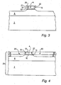
- the wafer 3 is coated with an oxide layer 16 as shown in Figure 2 .
- the oxide layer may be SiO 2 deposited by a plasma enhanced chemical vapour deposition (PECVD) process. It should, however, be noted that silicon nitride would be a suitable alternative choice to SiO 2 .
- the oxide layer 16 is photolithographicly patterned with a photoresist to leave a patterned mask 26, and etched to remove in areas not covered by the patterned mask the P 0 -layer 12, the active layer 10, and all but 200 nm of the buffer layer 8.
- layers 8, 10 and 12 are removed in a wet-etch process that undercuts the patterned mask 26 by about 200 nm to 500 nm.
- the layers 8, 10, and 12 are removed in all areas except along a mesa stripe 14 structure that extends perpendicular to the plane of the drawing, and which rises above the level of the substrate 2.
- the mesa stripe 14 has left and right opposite side walls 21,22 that together with the buffer layer 8 and the P 0 -layer 12 form a current conduction region 4 for an applied current I, and have the effect of guiding an optical mode 15 along the active layer 10 within the stripe 14.
- the width of the mesa stripe 14 varies depending on the particular device, but for opto-electronic devices such as laser diodes, the ridge stripe 14 is usually between 1 ⁇ m and 10 ⁇ m wide. The ridge strip 14 rises 1 ⁇ m to 2 ⁇ m above the surrounding substrate 2.
- a first current blocking structure 20 is then grown on the etched device up to approximately the level of the patterned mask 26, first with a p-doped InP layer 17, and then with an n-doped InP layer 18.
- the thicknesses of the p-doped and n-doped layers are similar. These InP layers 17,18 form a p-n junction that is insulating when the laser diode 1 is forward biased.
- the PECVD oxide layer 16 is removed with 10:1 buffered HF from the ridge strip 14 to expose again the P 0 -layer 12. This leaves an etched and coated wafer 23 comprising the substrate 2, the mesa stripe 14 and the first current blocking structure 20 abutting the opposite sides 21,22 of the mesa stripe 14.
- the etched and coated wafer 23 is coated with an oxide layer, such as an SiO 2 layer or silicon nitride layer deposited by PECVD, which is then pholithographicly patterned and etched as described above to leave a second patterned mask 36.
- the second patterned mask 36 is aligned along the length of the mesa stripe 14, but is wider than the mesa stripe, so that the mask 36 and extends at least 1 ⁇ m and preferably 2 ⁇ m laterally beyond the junction between each mesa side 21,22 and a top surface 37 of the P 0 -layer 12.
- the P 0 -layer 12, the active layer 10, and preferably all of the buffer layer 8 are then removed in a reactive ion plasma dry etch process, which cuts substantially vertical sides walls 41,42 through these layers.
- the resulting etched structure 44 is shown in Figure 5 .
- a second current blocking structure 45 is then grown using a MOVCD process on the exposed semiconductor surfaces of the etched structure 44.
- This current blocking structure is formed from a Fe-doped InP-based layer 46 topped by an n - -InP layer 47.
- the metal dopant could be ruthenium or chromium.
- the thickness of the Fe-InP layer is about 1 ⁇ m to 2 ⁇ m, so that this extends almost up to the mask 36.
- the n - -InP layer is about 200 nm to 500 nm thick, and extends just above the mask 36.
- the second current blocking structure 45 therefore abuts the side walls 41,42 of the first current blocking structure 20 along a substantially vertical interface, and the first current blocking structure 20 abuts the side walls 21,22 of the mesa stripe 14. Because the second current blocking structure 45 extends deeper within the current blocking region than the first current blocking structure 20, the second current blocking structure 45 also abuts a portion of the n - -InP buffer layer 8 along a substantially vertical interface.
- n - -InP layer 47 in the second blocking structure 45 blocks the conduction of holes through the blocking structure as well as acting as a barrier to the diffusion of Zn into the metal-doped layer 46.
- the patterned oxide layer 36 is removed with 10:1 buffered HF from the ridge strip 14 to expose again the P 0 -layer 12.
- a cladding layer 48 formed from p + -InP is then grown above the P 0 -layer 12 and current blocking structures 20,45 to a thickness of about 2 ⁇ m to 3 ⁇ m.
- the final semiconductor layer is a 100 nm to 200 nm thick ternary cap layer 49 deposited on the cladding layer 48.
- the cap layer 49 is formed from p ++ -GaInAs, highly doped to around 10 19 /cc, in order to provide a good low resistance ohmic contact for electrical connection to the current conduction region 4 of the mesa stripe 14.
- a ternary cap layer it is possible to use a quaternary InGaAsP cap layer.
- Metal 50 is then vacuum deposited on the cap layer 49 using well known techniques in two stages, first with a TiPt layer that is patterned using a lift-off process, and then final depositing of a TiAu layer, followed by metal wet etch in a photolithographically defined area. The remaining TiAu layer forms a contact pad 52 with good ohmic contact through the cap layer 49.
- the resulting wafer 54 is then thinned to a thickness of about 70 ⁇ m to 100 ⁇ m in a standard way, in order to assist with cleaving.
- the thinned wafer is then inscribed and cleaved in a conventional process first transversely into bars about 350 ⁇ m wide, and then each bar is cleaved into individual devices 200 ⁇ m wide.
- the cleaved device 1 is about 350 ⁇ m long (i.e. in the direction of the mesa 14) and about 200 ⁇ m wide.
- a Ti/Au metal layer 53 is then deposited by sputtering on the rear surface of the wafer, so enabling the device to be soldered onto a heat sink.
- the device 1 may be packaged in an industry standard package, with a single mode optical fibre coupled with a spherical lens to an output facet of the laser diode, and with gold bond wires soldered onto the metalised contact 52.
- the InGaAs/InP device 1 described above therefore incorporates a compound current confinement region formed from a reverse-biased p-n structure nearest the active region 10, and further away from the active region 10, a metal-doped InP-based layer.
- the p-n structure nearest the active region provides superior temperature performance, compared with a purely metal-doped current confinement region, while at the same time excess leakage current through the first current confinement structure at high operating frequencies due to parasitic capacitance from the reverse-biased diode structure is reduced owing to the reduced volume or amount of such a structure. Therefore, as will be described in further detail below, the invention provides a high resistivity current confinement region, and low leakage currents, across a wide range of operating temperatures. The invention also permits the use of higher drive voltages, which are useful in achieving high-speed operation.
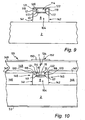
- Figures 8 to 10 show how the process described above may be modified, in a second embodiment 101 of the invention, where features corresponding with those of Figures 1 to 7 are given similar reference numerals incremented by 100.
- the process used to create the second embodiment 101 differs from that used to create the first embodiment 1 in that only one patterned inorganic mask 126 need be deposited on the wafer.
- This mask is used in the modified process in such a way that the mask 126 assures the self-alignment of the first current blocking structure 120 with respect to the second current blocking structure 145.
- the mask 126 is wider than the corresponding patterned mask shown in Figure 3 .
- the layers of the first current blocking structure 120, the p-doped InP layer 117 and n-doped InP layer 118 can still be grown up approximately to the level of the mask 126.
- the mask 126 is wide enough so that width of the first current blocking layer beneath the mask is sufficient for good highfrequency performance, as described above. Therefore, the first current blocking structure 120 and underlying buffer layer 8 outside the area of the mask 126 can be removed in a reactive ion plasma etching process, as shown in Figure 9 .
- the wafer is then processed in a similar manner to the first embodiment.
- the second current blocking structure 145 is formed with a 1 ⁇ m to 2 ⁇ m thick Fe-doped InP layer 146, overlain with a 200 nm to 500 nm thick n - -InP layer up to about the level of the top of the mesa strip 114.
- the mask 126 is then removed, followed by formation of the cladding layer 148, cap layer 149, metallic contact layer 150, and formation of a contacts 152,53 above the mesa stripe 114 and the substrate 2.
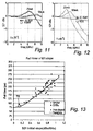
- FIG. 11 to 13 The performance of a semiconductor laser diode according to the invention is shown in Figures 11 to 13 .
- the small signal response against operating frequency at respectively 25°C and 85°C is shown respectively in Figures 11 and 12 , as a plot of the small signal initial slope S21 in dBo (dB optical) against operating frequency in GHz.
- the small signal drop off crosses -3 dB near 15 GHz.
- the signal fall time (90% to 10%) was measured to be about 85 ps. This is much better than the signal fall time of a standard buried heterostructure laser diode device with only a p-n junction current blocking layer either side of the mesa stripe, which is typically between 120 ps to 250 ps.
- Figure 13 shows a plot of fall time for the laser device of Figure 1 , within the circle labelled with reference numeral 70, compared against a range of other types of semiconductor laser devices. As can be seen, the typical fall time and S21 initial slope characteristics are very good.
- Semiconductor devices according to the invention provide a high operating bandwidth and good lifetime characteristics.
- the process steps involved may be similar to other standard steps used in the fabrication of such devices. There is no need for additional expensive processing equipment.
- the tolerances in the alignment of the mask or masks used to form the two current confinement structures are not unduly difficult to achieve using standard processing equipment.
- the present invention has been described specifically for the example of a laser diode, the invention is applicable to any high speed semiconductor device where current blocking regions help to channel current through a current conduction region, for example ridge waveguide type lasers, pump lasers, edge emitting light emitting diodes, edge photodetectors, surface emitting laser and light emitting diodes, and top-entry photodetectors.
- Another example is an optical waveguide with a split into two waveguides at a Y-junction. This may have electrically driven or modulated active optical regions in two or three of the arms of the "Y", for example an optical amplifier or modulator. It may then be desirable to provide a current blocking region at the junction of the three arms, where there may be three separate conduction regions.
- the invention described above have been described for a device based on an n -- -InP substrate, and having a first current blocking structure formed from a reverse biased p-n junction in laterally adjacent contact with the active layer structure, and a second current blocking structure formed from a metal-doped/n - InP layer structure in laterally adjacent contact with the first current blocking structure.
- the first current blocking structure may be a reverse biased n-p junction
- the second current blocking structure may include a metal-doped/p + InP layer structure in laterally adjacent contact with the first current blocking structure.
- the term "p-n junction current blocking structure" therefore includes such a reverse biased n-p junction.
Description
- The present invention relates to a semiconductor device with one or more current confinement regions and to a method of manufacturing such a device, particularly buried heterostructure light emitting devices such as semiconductor lasers and light emitting diodes.
- Buried heterostructure light emitting devices commonly have current confinement regions defined by areas of high resistivity that channel current to an optically active layer within the structure. In devices using InGaAsP/InP materials, current confinement regions have been employed based on a reverse-biased p-n or n-p diode structure. Such structures provide high resistivity, and low leakage currents, and are widely used in fibre optic communication systems across a range of operating frequencies. At operating frequencies about 1 GHz, however, the performance of such devices becomes limited by the capacitance of the current blocking structure, owing to the charge on the reverse biased diode junction.
- Other current blocking structures have therefore been developed, for example Fe-doped InP-based layers, as described in
US patent 4,660,208 . Such Fe-doped layers have a lower capacitance than structures based on a reverse biased junction, but do not have as high a resistivity. This lower resistivity also limits operation and device lifetime at high frequencies, because of the resulting higher device operating temperatures. In order to avoid excessive temperatures, it becomes necessary to use a lower drive voltage, and this in turn limits the achievable bandwidth of a device based on Fe-doped material. -
EP-A-0 547 850 andUS-A-5 636 237 both disclose a semiconductor laser device comprising an active layer and a mesa-stripe shaped current conduction region, with a current confinement region located on either side of the current conduction region, the current conduction region and current confinement region being arranged to channel electric current to the active layer, wherein each current confinement region includes both a metal-doped current blocking structure (Fe doped InP) and a p-n junction current blocking structure, the p-n current blocking structure being grown adjacent the active layer, between the current conduction region and the metal-doped current blocking structure. - In
EP-A-0 547 850 the layers of the p-n junction current blocking structure are etched with a photolithography technique, which cuts curved side walls through these layers, and the metal doped current blocking structure is subsequently grown adjacent to these curved side walls of the p-n junction current blocking structure. - In
US-A-5 636 237 the p-n junction current blocking structure is deposited with curved side walls, and the metal doped current blocking structure is subsequently grown adjacent to the outermost curved side wall of the p-n junction current blocking structure. - In recent years there has been an increasing demand for fibre optic communication links having a bandwidth in excess of 1 GHz, for example up to 10 GHz. It is an object of the present invention to provide a semiconductor device that addresses these issues.
- Accordingly, the invention provides a semiconductor device comprising an active layer, a current conduction region, one or more current confinement regions adjacent the current conduction region, the current conduction region and current confinement region being arranged to channel electric current to the active layer, wherein the or each current confinement region includes both a metal-doped current blocking structure and a p-n junction current blocking structure, the p-n current blocking structure being between the current conduction region and the metal-doped current blocking structure and wherein the metal-doped current blocking structure abuts the p-n current blocking structure along a substantially vertical interface.
- It has been found that the p-n current blocking structure nearest the current conduction region then provides high resistivity and good high frequency performance at high temperatures, while the reduction in the volume of the p-n current blocking structure and use of the metal-doped second current blocking structure further away from the current conduction region provides reduced parasitic capacitance.
- In some types of device, for example buried heterostructure laser diodes, the device includes a substrate, a mesa stripe on the substrate and the active layer in the mesa stripe. The current conduction region then channels current through the active layer.
- The mesa stripe may have side walls that rise above the substrate. The active layer then extends to the side walls and the active layer is covered at the side walls by the p-n blocking structure.
- In preferred embodiments of the invention, the mesa side walls slope laterally away from the active layer towards the metal-doped current blocking structure.
- Also according to the invention, there is provided a method of forming a semiconductor device comprising an active layer, a current conduction region, one or more current confinement regions adjacent the current conduction region, the current conduction region and current confinement region being arranged to channel electric current to the active layer, wherein the method comprises the steps of:
- i) growing upon a semiconductor substrate a plurality of semiconductor layers, including a buffer layer, the active layer and the current conduction region by which electric current may be applied to the active layer;
- ii) growing adjacent the active layer a p-n junction current blocking structure;
- iii) cutting substantially vertical side walls through the grown layers in a reactive ion plasma dry etch process; and
- iv) growing adjacent the substantially vertical side walls of the p-n junction current blocking structure a metal-doped current blocking structure such that the metal-doped current blocking structure abuts the p-n current blocking structure along a substantially vertical interface, the p-n junction current blocking structure and the metal-doped current blocking structure together forming a current confinement region for channelling electric current to the current conduction region.
- In one embodiment of the invention, prior to step ii), a first etch mask is formed over the active layer, said first etch mask defining during a first etching process an area of the active layer adjacent the current conduction region to be removed by the etching. Then, prior to step iii) a second etch mask is formed over the active layer and the p-n junction current blocking structure adjacent the current conduction region, said second etch mask defining during the reactive ion plasma dry etch process an area of p-n junction current blocking structure not adjacent the active layer to be removed by the etching.
- This second etch mask may then remain in place during the growth of the metal-doped current blocking structure in step iii).
- In order to achieve a sufficiently uniform width of the first current blocking structure, the second etch mask is then aligned laterally with the first etch mask, typically to an accuracy of about 10% to 20% of the width of the second etch mask. In one preferred embodiment of the invention, the second etch mask is laterally wider than the first etch mask.
- In another embodiment of the invention, prior to step ii), an etch mask is formed over the active layer, said etch mask defining during a first etching process an area of the active layer adjacent the current conduction region to be removed by the etching. The etch mask remains during the growth of the p-n current blocking structure in step ii). Finally, the etch mask also defines during the reactive ion plasma dry etch process an area of the p-n junction current blocking structure not adjacent the active layer to be removed by the etching.
- This etch mask may then remain in place during the growth of the metal-doped current blocking structure in step iii).
- Because this process uses only one mask for the formation of the first current blocking structure and the second current blocking structure, the process is self-aligning for these two current blocking structures.
- The invention will now be described by way of example, with reference to the accompanying drawings, in which:
-
Figure 1 is a schematic cross-section of a buried heterostructure semiconductor laser device according to a first embodiment of the invention, comprising an active layer within a buried mesa stripe, a current conduction region for channelling current to the active layer, and current confinement regions consisting of two distinct current confinement structures on each side of the heterostructure; -
Figures 2 to 4 show process steps for creating a first current confinement structure adjacent the mesa stripe, formed from a p-n junction current blocking layer; -
Figures 5 and 6 show process steps for creating a second current confinement structure adjacent the first current blocking layer, formed from a metal-doped current blocking layer; -
Figure 7 shows the formation of cladding, cap, and electrical contact layers leading to the device ofFigure 1 ; -
Figures 8 to 10 show process steps for a second embodiment of the invention; -
Figure 11 and 12 show plots of small signal response against operating frequency at respectively 25°C and 85°C for the laser device ofFigure 1 ; and -
Figure 13 shows a plot of fall time against small signal response for the laser device ofFigure 1 , and for a various types of known semiconductor laser device. -
Figure 1 shows, not to scale, a cross-section of asemiconductor device 1 according to the invention, here a buried heterostructure laser diode suitable for use as a transmitter in a high speed fibre-optic link operating at 1.55 µm. Currently, high speed links operate at 2.5 or 10 Gbits/s, and bit rates of up to 40 Gbits/s have been demonstrated in the laboratory. - Referring now also to
Figure 2 , thedevice 1 is formed starting from awafer 3 that is 32 mm square, and that has an n---InP substrate 2 doped to around 1019/cc, on which is grown a 2 µm thick n--InP buffer layer 8 doped to around 1018/cc. Anactive layer 10 is grown on thebuffer layer 8 according to known techniques for fabricating planar active lasers for a laser diode - the active layer could be a bulk region or a strained multiple quantum well (SMQW) structure. An example of an SMQW device is discussed in W. S. Ring et al, Optical Fibre Conference, Vol. 2, 1996 Technical Digest Series, Optical Society of America. The type of active layer employed is not critical to the invention. - In the present example, the
laser diode 1 has a quaternary InxGa1-xAs1-yPyactive layer 10 that may be between about 100 nm to 300 nm thick. Theactive layer 10 is topped by anotherbuffer layer 12, also called a P0-layer, formed from p+-InP, grown to be between about 400 nm to 1 µm thick. - Although not illustrated a DFB grating for the
laser diode 1 can be contained in the n--InP buffer layer 8 or in an additional p-InGaAsP grating layer. - Then, using well-known fabrication technology, the
wafer 3 is coated with an oxide layer 16 as shown inFigure 2 . The oxide layer may be SiO2 deposited by a plasma enhanced chemical vapour deposition (PECVD) process. It should, however, be noted that silicon nitride would be a suitable alternative choice to SiO2. As shown inFigure 3 , the oxide layer 16 is photolithographicly patterned with a photoresist to leave apatterned mask 26, and etched to remove in areas not covered by the patterned mask the P0-layer 12, theactive layer 10, and all but 200 nm of thebuffer layer 8. In thisexample layers mask 26 by about 200 nm to 500 nm. - The
layers mesa stripe 14 structure that extends perpendicular to the plane of the drawing, and which rises above the level of thesubstrate 2. Themesa stripe 14 has left and rightopposite side walls buffer layer 8 and the P0-layer 12 form acurrent conduction region 4 for an applied current I, and have the effect of guiding anoptical mode 15 along theactive layer 10 within thestripe 14. - The width of the
mesa stripe 14 varies depending on the particular device, but for opto-electronic devices such as laser diodes, theridge stripe 14 is usually between 1 µm and 10 µm wide. Theridge strip 14 rises 1 µm to 2 µm above the surroundingsubstrate 2. - A first
current blocking structure 20 is then grown on the etched device up to approximately the level of the patternedmask 26, first with a p-dopedInP layer 17, and then with an n-dopedInP layer 18. The thicknesses of the p-doped and n-doped layers are similar. These InP layers 17,18 form a p-n junction that is insulating when thelaser diode 1 is forward biased. - After deposition of the first
current blocking structure 20, the PECVD oxide layer 16 is removed with 10:1 buffered HF from theridge strip 14 to expose again the P0-layer 12. This leaves an etched andcoated wafer 23 comprising thesubstrate 2, themesa stripe 14 and the firstcurrent blocking structure 20 abutting theopposite sides mesa stripe 14. - The etched and
coated wafer 23 is coated with an oxide layer, such as an SiO2 layer or silicon nitride layer deposited by PECVD, which is then pholithographicly patterned and etched as described above to leave a second patternedmask 36. The second patternedmask 36 is aligned along the length of themesa stripe 14, but is wider than the mesa stripe, so that themask 36 and extends at least 1 µm and preferably 2 µm laterally beyond the junction between eachmesa side layer 12. - The P0-
layer 12, theactive layer 10, and preferably all of thebuffer layer 8 are then removed in a reactive ion plasma dry etch process, which cuts substantiallyvertical sides walls structure 44 is shown inFigure 5 . - A second
current blocking structure 45 is then grown using a MOVCD process on the exposed semiconductor surfaces of the etchedstructure 44. This current blocking structure is formed from a Fe-doped InP-basedlayer 46 topped by an n--InP layer 47. Alternatively, instead of iron, the metal dopant could be ruthenium or chromium. The thickness of the Fe-InP layer is about 1 µm to 2 µm, so that this extends almost up to themask 36. The n--InP layer is about 200 nm to 500 nm thick, and extends just above themask 36. The secondcurrent blocking structure 45 therefore abuts theside walls current blocking structure 20 along a substantially vertical interface, and the firstcurrent blocking structure 20 abuts theside walls mesa stripe 14. Because the secondcurrent blocking structure 45 extends deeper within the current blocking region than the firstcurrent blocking structure 20, the secondcurrent blocking structure 45 also abuts a portion of the n--InP buffer layer 8 along a substantially vertical interface. - The n--
InP layer 47 in thesecond blocking structure 45 blocks the conduction of holes through the blocking structure as well as acting as a barrier to the diffusion of Zn into the metal-dopedlayer 46. - After the growth of the second
current confinement structure 45, the patternedoxide layer 36 is removed with 10:1 buffered HF from theridge strip 14 to expose again the P0-layer 12. - A
cladding layer 48 formed from p+-InP is then grown above the P0-layer 12 andcurrent blocking structures ternary cap layer 49 deposited on thecladding layer 48. Thecap layer 49 is formed from p++-GaInAs, highly doped to around 1019/cc, in order to provide a good low resistance ohmic contact for electrical connection to thecurrent conduction region 4 of themesa stripe 14. As an alternative to a ternary cap layer, it is possible to use a quaternary InGaAsP cap layer. -
Metal 50 is then vacuum deposited on thecap layer 49 using well known techniques in two stages, first with a TiPt layer that is patterned using a lift-off process, and then final depositing of a TiAu layer, followed by metal wet etch in a photolithographically defined area. The remaining TiAu layer forms acontact pad 52 with good ohmic contact through thecap layer 49. - The resulting wafer 54 is then thinned to a thickness of about 70 µm to 100 µm in a standard way, in order to assist with cleaving. The thinned wafer is then inscribed and cleaved in a conventional process first transversely into bars about 350 µm wide, and then each bar is cleaved into
individual devices 200 µm wide. Thecleaved device 1 is about 350 µm long (i.e. in the direction of the mesa 14) and about 200 µm wide. - A Ti/
Au metal layer 53 is then deposited by sputtering on the rear surface of the wafer, so enabling the device to be soldered onto a heat sink. - Although not shown, after testing the
device 1 may be packaged in an industry standard package, with a single mode optical fibre coupled with a spherical lens to an output facet of the laser diode, and with gold bond wires soldered onto themetalised contact 52. - The InGaAs/
InP device 1 described above therefore incorporates a compound current confinement region formed from a reverse-biased p-n structure nearest theactive region 10, and further away from theactive region 10, a metal-doped InP-based layer. The p-n structure nearest the active region provides superior temperature performance, compared with a purely metal-doped current confinement region, while at the same time excess leakage current through the first current confinement structure at high operating frequencies due to parasitic capacitance from the reverse-biased diode structure is reduced owing to the reduced volume or amount of such a structure. Therefore, as will be described in further detail below, the invention provides a high resistivity current confinement region, and low leakage currents, across a wide range of operating temperatures. The invention also permits the use of higher drive voltages, which are useful in achieving high-speed operation. -
Figures 8 to 10 show how the process described above may be modified, in asecond embodiment 101 of the invention, where features corresponding with those ofFigures 1 to 7 are given similar reference numerals incremented by 100. The process used to create thesecond embodiment 101 differs from that used to create thefirst embodiment 1 in that only one patternedinorganic mask 126 need be deposited on the wafer. This mask is used in the modified process in such a way that themask 126 assures the self-alignment of the firstcurrent blocking structure 120 with respect to the secondcurrent blocking structure 145. - Here, the
mask 126 is wider than the corresponding patterned mask shown inFigure 3 . However, the layers of the firstcurrent blocking structure 120, the p-dopedInP layer 117 and n-dopedInP layer 118, can still be grown up approximately to the level of themask 126. Themask 126 is wide enough so that width of the first current blocking layer beneath the mask is sufficient for good highfrequency performance, as described above. Therefore, the firstcurrent blocking structure 120 andunderlying buffer layer 8 outside the area of themask 126 can be removed in a reactive ion plasma etching process, as shown inFigure 9 . - The wafer is then processed in a similar manner to the first embodiment. The second
current blocking structure 145 is formed with a 1 µm to 2 µm thick Fe-dopedInP layer 146, overlain with a 200 nm to 500 nm thick n--InP layer up to about the level of the top of themesa strip 114. Themask 126 is then removed, followed by formation of thecladding layer 148,cap layer 149,metallic contact layer 150, and formation of acontacts mesa stripe 114 and thesubstrate 2. - The performance of a semiconductor laser diode according to the invention is shown in
Figures 11 to 13 . The small signal response against operating frequency at respectively 25°C and 85°C is shown respectively inFigures 11 and 12 , as a plot of the small signal initial slope S21 in dBo (dB optical) against operating frequency in GHz. The small signal drop off crosses -3 dB near 15 GHz. The signal fall time (90% to 10%) was measured to be about 85 ps. This is much better than the signal fall time of a standard buried heterostructure laser diode device with only a p-n junction current blocking layer either side of the mesa stripe, which is typically between 120 ps to 250 ps. - In order to test the efficiency of the laser diodes, dc measurements of the slope of the light output vs drive current were made at 25°C and at 85°C. The slopes at typical drive currents of 8.5 mA (at 25°C) and 29 mA (at 85°C) were measured and then divided by the slopes at about 1 mA. The ratio of these slopes is a measure of the device's efficiency, which was determined to be 0.86 at 25°C and 0.71 at 85°. For devices of this sort, efficiency figures such as this are considered to be very good.
-
Figure 13 shows a plot of fall time for the laser device ofFigure 1 , within the circle labelled withreference numeral 70, compared against a range of other types of semiconductor laser devices. As can be seen, the typical fall time and S21 initial slope characteristics are very good. - Semiconductor devices according to the invention provide a high operating bandwidth and good lifetime characteristics. The process steps involved may be similar to other standard steps used in the fabrication of such devices. There is no need for additional expensive processing equipment. The tolerances in the alignment of the mask or masks used to form the two current confinement structures are not unduly difficult to achieve using standard processing equipment.
- Although the present invention has been described specifically for the example of a laser diode, the invention is applicable to any high speed semiconductor device where current blocking regions help to channel current through a current conduction region, for example ridge waveguide type lasers, pump lasers, edge emitting light emitting diodes, edge photodetectors, surface emitting laser and light emitting diodes, and top-entry photodetectors. Another example is an optical waveguide with a split into two waveguides at a Y-junction. This may have electrically driven or modulated active optical regions in two or three of the arms of the "Y", for example an optical amplifier or modulator. It may then be desirable to provide a current blocking region at the junction of the three arms, where there may be three separate conduction regions.
- The invention described above have been described for a device based on an n---InP substrate, and having a first current blocking structure formed from a reverse biased p-n junction in laterally adjacent contact with the active layer structure, and a second current blocking structure formed from a metal-doped/n- InP layer structure in laterally adjacent contact with the first current blocking structure. However, it is to be appreciated that the invention can also be applied to other types of devices, for example those based on a p++-InP substrate. In this case, the first current blocking structure may be a reverse biased n-p junction, and the second current blocking structure may include a metal-doped/p+ InP layer structure in laterally adjacent contact with the first current blocking structure. The term "p-n junction current blocking structure" therefore includes such a reverse biased n-p junction.
Claims (9)
- A semiconductor device (1, 101) comprising an active layer (10), a current conduction region (4;104), one or more current confinement regions (20,45;120,145) adjacent the current conduction region, the current conduction region (4;104) and current confinement region (20,45;120,145) being arranged to channel electric current to the active layer (10), wherein the or each current confinement region includes both a metal-doped current blocking structure (45;145) and a p-n junction current blocking structure (20;120), the p-n current blocking structure (20;120) being between the current conduction region (4;104) and the metal-doped current blocking structure (45;145), and wherein the metal-doped current blocking structure (45;145) abuts the p-n current blocking structure (20,-120) along a substantially vertical interface (41,42;141,142).
- A semiconductor device as claimed in Claim 1, the device including a substrate (2), a mesa stripe (14;114) on the substrate (2) and the active layer (10) in the mesa stripe (14;114), in which the current conduction region (4;104) channels current through the active layer (10).
- A semiconductor device as claimed in Claim 2, in which the mesa stripe (14;114) has side walls (21,22;121,122) that rise above the substrate (2), the active layer (10) extending to the side walls (21,22;121,122) and the active layer (10) being covered at the side walls (21,22;121,122) by the p-n blocking structure (20;120).
- A semiconductor device (1) as claimed in Claim 2 or Claim 3, in which the mesa side walls (21,22;121,122) slope laterally away from the active layer (10) towards the metal-doped current blocking structure (45;145).
- A semiconductor device (1) as claimed in any previous claim, in which the device (1) is a buried heterostructure laser diode device.
- A semiconductor device (1) as claimed in any preceding claim, in which the device (1) is formed from III-V semiconductor materials.
- A method of forming a semiconductor device (1,101) comprising an active layer (10), a current conduction region (4;104), one or more current confinement regions (20,45;120,145) adjacent the current conduction region, the current conduction region (4;104) and current confinement region (20,45;120,145) being arranged to channel electric current to the active layer (10), wherein the method comprises the steps of:i) growing upon a semiconductor substrate (2) a plurality of semiconductor layers, including a buffer layer (8), the active layer (10) and the current conduction region (4;104) by which electric current may be applied to the active layer (10);ii) growing adjacent the active layer (10) a p-n junction current blocking structure (20;120),iii) cutting substantially vertical sides walls (41,42) through the grown layers in a reactive ion plasma dry etch process, andiv) growing adjacent the substantially vertical side walls of the p-n junction current blocking structure (20;120) a metal-doped current blocking structure (45;145) such that the metal-doped current blocking structure abuts the p-n current blocking structure along a substantially vertical interface, the p-n junction current blocking structure and the metal-doped current blocking structure (45;145) together forming a current confinement region for channelling electric current to the current conduction region (4;104).
- A method as claimed in Claim 7, in which:prior to step ii) a first etch mask (26) is formed over the active layer (10), said first etch mask (26) defining during a first etching process an area of the active layer adjacent the current conduction region (4) to be removed by the etching; andprior to step iii) a second etch mask (36) is formed over the active layer (10) and the p-n junction current blocking structure (20) adjacent the current conduction region (4), said second etch mask (36) defining during said reactive ion plasma dry etch process an area of p-n junction current blocking structure (20) not adjacent the active layer (10) to be removed by the etching.
- A method as claimed in Claim 7, in which:prior to step ii) , an etch mask (126) is formed over the active layer (10), said etch mask defining during a first etching process an area of the active layer adjacent the current conduction region (104) to be removed by the etching;said first etch mask (126) remains during the growth of the p-n current blocking structure (120) in step ii); andsaid etch mask (126) also defines during said reactive ion plasma dry etch process an area of the p-n junction current blocking structure (20) not adjacent the active layer (10) to be removed by the etching.
Priority Applications (4)
| Application Number | Priority Date | Filing Date | Title |
|---|---|---|---|
| EP01300447A EP1225670B1 (en) | 2001-01-18 | 2001-01-18 | Semiconductor device with current confinement structure |
| DE60136261T DE60136261D1 (en) | 2001-01-18 | 2001-01-18 | Semiconductor device with current limiting structure |
| US09/858,677 US6509580B2 (en) | 2001-01-18 | 2001-05-16 | Semiconductor device with current confinement structure |
| JP2002005692A JP2002232080A (en) | 2001-01-18 | 2002-01-15 | Semiconductor element having current confining structure and its manufacturing method |
Applications Claiming Priority (1)
| Application Number | Priority Date | Filing Date | Title |
|---|---|---|---|
| EP01300447A EP1225670B1 (en) | 2001-01-18 | 2001-01-18 | Semiconductor device with current confinement structure |
Publications (2)
| Publication Number | Publication Date |
|---|---|
| EP1225670A1 EP1225670A1 (en) | 2002-07-24 |
| EP1225670B1 true EP1225670B1 (en) | 2008-10-22 |
Family
ID=8181652
Family Applications (1)
| Application Number | Title | Priority Date | Filing Date |
|---|---|---|---|
| EP01300447A Expired - Lifetime EP1225670B1 (en) | 2001-01-18 | 2001-01-18 | Semiconductor device with current confinement structure |
Country Status (4)
| Country | Link |
|---|---|
| US (1) | US6509580B2 (en) |
| EP (1) | EP1225670B1 (en) |
| JP (1) | JP2002232080A (en) |
| DE (1) | DE60136261D1 (en) |
Cited By (1)
| Publication number | Priority date | Publication date | Assignee | Title |
|---|---|---|---|---|
| DE102010026518A1 (en) * | 2010-07-08 | 2012-01-12 | Osram Opto Semiconductors Gmbh | Light-emitting diode chip and method for producing a light-emitting diode chip |
Families Citing this family (9)
| Publication number | Priority date | Publication date | Assignee | Title |
|---|---|---|---|---|
| DE10108079A1 (en) * | 2000-05-30 | 2002-09-12 | Osram Opto Semiconductors Gmbh | Optically-pumped surface-emitting semiconductor laser device, has edge-emitting structure of pumping source and radiation-emitting quantum pot type structure applied to common substrate |
| US6829275B2 (en) * | 2001-12-20 | 2004-12-07 | Bookham Technology, Plc | Hybrid confinement layers of buried heterostructure semiconductor laser |
| EP1372228B1 (en) * | 2002-06-12 | 2006-10-04 | Agilent Technologies, Inc. - a Delaware corporation - | Integrated semiconductor laser and waveguide device |
| EP1372229B1 (en) * | 2002-06-12 | 2006-02-15 | Agilent Technologies Inc., A Delaware Corporation | Integrated semiconductor laser and waveguide device |
| KR100547830B1 (en) * | 2003-08-13 | 2006-01-31 | 삼성전자주식회사 | Integrated optical device and manufacturing method |
| US7009214B2 (en) | 2003-10-17 | 2006-03-07 | Atomic Energy Council —Institute of Nuclear Energy Research | Light-emitting device with a current blocking structure and method for making the same |
| JP2005260109A (en) * | 2004-03-15 | 2005-09-22 | Fujitsu Ltd | Optical semiconductor element |
| JP5803366B2 (en) * | 2011-07-14 | 2015-11-04 | 住友電気工業株式会社 | Method of manufacturing buried heterostructure semiconductor laser and buried heterostructure semiconductor laser |
| US11133649B2 (en) * | 2019-06-21 | 2021-09-28 | Palo Alto Research Center Incorporated | Index and gain coupled distributed feedback laser |
Family Cites Families (11)
| Publication number | Priority date | Publication date | Assignee | Title |
|---|---|---|---|---|
| US4425650A (en) * | 1980-04-15 | 1984-01-10 | Nippon Electric Co., Ltd. | Buried heterostructure laser diode |
| JPH06507046A (en) * | 1991-05-07 | 1994-08-04 | ブリテイッシュ・テレコミュニケーションズ・パブリック・リミテッド・カンパニー | optical clock extraction |
| JPH05167191A (en) * | 1991-12-18 | 1993-07-02 | Furukawa Electric Co Ltd:The | Buried type semiconductor laser element |
| JPH0722691A (en) * | 1993-06-30 | 1995-01-24 | Mitsubishi Electric Corp | Semiconductor laser and manufacture thereof |
| EP0639875A1 (en) * | 1993-07-12 | 1995-02-22 | BRITISH TELECOMMUNICATIONS public limited company | Electrical barrier structure for semiconductor device |
| JPH0851250A (en) * | 1994-08-09 | 1996-02-20 | Mitsubishi Electric Corp | Semiconductor laser |
| US5832019A (en) * | 1994-11-28 | 1998-11-03 | Xerox Corporation | Index guided semiconductor laser biode with shallow selective IILD |
| JP3386261B2 (en) * | 1994-12-05 | 2003-03-17 | 三菱電機株式会社 | Optical semiconductor device and method of manufacturing the same |
| JPH08213691A (en) * | 1995-01-31 | 1996-08-20 | Nec Corp | Semiconductor laser |
| JPH0918079A (en) * | 1995-06-27 | 1997-01-17 | Mitsubishi Electric Corp | Semiconductor device and manufacture thereof |
| JP3241002B2 (en) * | 1998-09-02 | 2001-12-25 | 日本電気株式会社 | Manufacturing method of semiconductor laser |
-
2001
- 2001-01-18 EP EP01300447A patent/EP1225670B1/en not_active Expired - Lifetime
- 2001-01-18 DE DE60136261T patent/DE60136261D1/en not_active Expired - Fee Related
- 2001-05-16 US US09/858,677 patent/US6509580B2/en not_active Expired - Lifetime
-
2002
- 2002-01-15 JP JP2002005692A patent/JP2002232080A/en not_active Withdrawn
Cited By (1)
| Publication number | Priority date | Publication date | Assignee | Title |
|---|---|---|---|---|
| DE102010026518A1 (en) * | 2010-07-08 | 2012-01-12 | Osram Opto Semiconductors Gmbh | Light-emitting diode chip and method for producing a light-emitting diode chip |
Also Published As
| Publication number | Publication date |
|---|---|
| DE60136261D1 (en) | 2008-12-04 |
| US6509580B2 (en) | 2003-01-21 |
| JP2002232080A (en) | 2002-08-16 |
| EP1225670A1 (en) | 2002-07-24 |
| US20020093013A1 (en) | 2002-07-18 |
Similar Documents
| Publication | Publication Date | Title |
|---|---|---|
| AU651111B2 (en) | Optoelectronic device | |
| EP0437836A2 (en) | Optical semiconductor device | |
| US8558245B2 (en) | Optical semiconductor device having ridge structure formed on active layer containing p-type region and its manufacture method | |
| US6995454B2 (en) | Semiconductor optical integrated device having a light emitting portion, a modulation section and a separation portion | |
| EP1225670B1 (en) | Semiconductor device with current confinement structure | |
| EP0917260A1 (en) | Electrical isolation of opto-electronic device components | |
| Deimel | Micromachining processes and structures in micro-optics and optoelectronics | |
| EP1372228B1 (en) | Integrated semiconductor laser and waveguide device | |
| JP3306802B2 (en) | Photon integrated circuit and method of manufacturing the same | |
| CN111129945B (en) | Method for integrally manufacturing isolator-saving edge-emitting laser chip | |
| US20050185689A1 (en) | Optoelectronic device having a Discrete Bragg Reflector and an electro-absorption modulator | |
| EP0581604A2 (en) | A semiconductor laser device | |
| EP1134858A1 (en) | Buried mesa semiconductor device | |
| EP1300917A1 (en) | Semiconductor device with current confinement structure | |
| CA2033246C (en) | Optical semiconductor device | |
| EP1372229B1 (en) | Integrated semiconductor laser and waveguide device | |
| US20050078724A1 (en) | Single mode distributed feedback lasers | |
| US6751246B2 (en) | Buried ribbon semiconductor laser and a method of fabrication | |
| EP1339108A1 (en) | Semiconductor device with current confinement structure | |
| US7286588B2 (en) | Semiconductor laser with grating structure for stabilizing the wavelength of optical radiation | |
| GB2620487A (en) | Photonic devices with improved lateral current confinement | |
| CN114678767A (en) | Semiconductor optical device and method for manufacturing the same | |
| JPH1012972A (en) | Optical semiconductor device and its manufacture |
Legal Events
| Date | Code | Title | Description |
|---|---|---|---|
| PUAI | Public reference made under article 153(3) epc to a published international application that has entered the european phase |
Free format text: ORIGINAL CODE: 0009012 |
|
| AK | Designated contracting states |
Kind code of ref document: A1 Designated state(s): AT BE CH CY DE DK ES FI FR GB GR IE IT LI LU MC NL PT SE TR |
|
| AX | Request for extension of the european patent |
Free format text: AL;LT;LV;MK;RO;SI |
|
| 17P | Request for examination filed |
Effective date: 20030124 |
|
| AKX | Designation fees paid |
Designated state(s): DE FR GB |
|
| RAP1 | Party data changed (applicant data changed or rights of an application transferred) |
Owner name: AVAGO TECHNOLOGIES FIBER IP (SINGAPORE) PTE. LTD. |
|
| 17Q | First examination report despatched |
Effective date: 20071001 |
|
| GRAP | Despatch of communication of intention to grant a patent |
Free format text: ORIGINAL CODE: EPIDOSNIGR1 |
|
| GRAS | Grant fee paid |
Free format text: ORIGINAL CODE: EPIDOSNIGR3 |
|
| GRAA | (expected) grant |
Free format text: ORIGINAL CODE: 0009210 |
|
| AK | Designated contracting states |
Kind code of ref document: B1 Designated state(s): DE FR GB |
|
| REG | Reference to a national code |
Ref country code: GB Ref legal event code: FG4D |
|
| REF | Corresponds to: |
Ref document number: 60136261 Country of ref document: DE Date of ref document: 20081204 Kind code of ref document: P |
|
| PLBE | No opposition filed within time limit |
Free format text: ORIGINAL CODE: 0009261 |
|
| STAA | Information on the status of an ep patent application or granted ep patent |
Free format text: STATUS: NO OPPOSITION FILED WITHIN TIME LIMIT |
|
| 26N | No opposition filed |
Effective date: 20090723 |
|
| PG25 | Lapsed in a contracting state [announced via postgrant information from national office to epo] |
Ref country code: DE Free format text: LAPSE BECAUSE OF NON-PAYMENT OF DUE FEES Effective date: 20090801 |
|
| REG | Reference to a national code |
Ref country code: FR Ref legal event code: ST Effective date: 20091030 |
|
| PG25 | Lapsed in a contracting state [announced via postgrant information from national office to epo] |
Ref country code: FR Free format text: LAPSE BECAUSE OF NON-PAYMENT OF DUE FEES Effective date: 20090202 |
|
| REG | Reference to a national code |
Ref country code: GB Ref legal event code: 732E Free format text: REGISTERED BETWEEN 20130725 AND 20130731 |
|
| PGFP | Annual fee paid to national office [announced via postgrant information from national office to epo] |
Ref country code: GB Payment date: 20151224 Year of fee payment: 16 |
|
| GBPC | Gb: european patent ceased through non-payment of renewal fee |
Effective date: 20170118 |
|
| PG25 | Lapsed in a contracting state [announced via postgrant information from national office to epo] |
Ref country code: GB Free format text: LAPSE BECAUSE OF NON-PAYMENT OF DUE FEES Effective date: 20170118 |