EP0437836A2 - Optical semiconductor device - Google Patents
Optical semiconductor device Download PDFInfo
- Publication number
- EP0437836A2 EP0437836A2 EP90125516A EP90125516A EP0437836A2 EP 0437836 A2 EP0437836 A2 EP 0437836A2 EP 90125516 A EP90125516 A EP 90125516A EP 90125516 A EP90125516 A EP 90125516A EP 0437836 A2 EP0437836 A2 EP 0437836A2
- Authority
- EP
- European Patent Office
- Prior art keywords
- layer
- stripe
- semi
- mesa structure
- semiconductor device
- Prior art date
- Legal status (The legal status is an assumption and is not a legal conclusion. Google has not performed a legal analysis and makes no representation as to the accuracy of the status listed.)
- Granted
Links
- 230000003287 optical effect Effects 0.000 title claims abstract description 151
- 239000004065 semiconductor Substances 0.000 title claims abstract description 51
- 238000005253 cladding Methods 0.000 claims abstract description 64
- 239000000758 substrate Substances 0.000 claims abstract description 64
- 230000031700 light absorption Effects 0.000 claims abstract description 44
- 230000005684 electric field Effects 0.000 claims description 11
- 239000000203 mixture Substances 0.000 claims description 7
- 230000008878 coupling Effects 0.000 claims 1
- 238000010168 coupling process Methods 0.000 claims 1
- 238000005859 coupling reaction Methods 0.000 claims 1
- 230000003247 decreasing effect Effects 0.000 abstract description 10
- VYPSYNLAJGMNEJ-UHFFFAOYSA-N Silicium dioxide Chemical compound O=[Si]=O VYPSYNLAJGMNEJ-UHFFFAOYSA-N 0.000 description 39
- 229910052681 coesite Inorganic materials 0.000 description 21
- 229910052906 cristobalite Inorganic materials 0.000 description 21
- 239000000377 silicon dioxide Substances 0.000 description 21
- 229910052682 stishovite Inorganic materials 0.000 description 21
- 229910052905 tridymite Inorganic materials 0.000 description 21
- 238000005530 etching Methods 0.000 description 20
- 238000000034 method Methods 0.000 description 20
- 235000012239 silicon dioxide Nutrition 0.000 description 18
- 229910000530 Gallium indium arsenide Inorganic materials 0.000 description 11
- 238000004519 manufacturing process Methods 0.000 description 11
- 239000004642 Polyimide Substances 0.000 description 8
- 239000000463 material Substances 0.000 description 8
- 229920001721 polyimide Polymers 0.000 description 8
- 230000000694 effects Effects 0.000 description 7
- 238000000206 photolithography Methods 0.000 description 6
- 238000010521 absorption reaction Methods 0.000 description 5
- 230000003068 static effect Effects 0.000 description 5
- 230000005540 biological transmission Effects 0.000 description 4
- 238000004891 communication Methods 0.000 description 4
- 238000002488 metal-organic chemical vapour deposition Methods 0.000 description 4
- 229920002120 photoresistant polymer Polymers 0.000 description 4
- 229910001218 Gallium arsenide Inorganic materials 0.000 description 3
- 229910021417 amorphous silicon Inorganic materials 0.000 description 3
- 238000012538 light obscuration Methods 0.000 description 3
- 238000000927 vapour-phase epitaxy Methods 0.000 description 3
- 229910000980 Aluminium gallium arsenide Inorganic materials 0.000 description 2
- 239000003989 dielectric material Substances 0.000 description 2
- 150000002500 ions Chemical class 0.000 description 2
- 238000007747 plating Methods 0.000 description 2
- 238000000926 separation method Methods 0.000 description 2
- 239000000126 substance Substances 0.000 description 2
- 229910004205 SiNX Inorganic materials 0.000 description 1
- 230000015572 biosynthetic process Effects 0.000 description 1
- 229910052793 cadmium Inorganic materials 0.000 description 1
- 238000004364 calculation method Methods 0.000 description 1
- 238000003486 chemical etching Methods 0.000 description 1
- 238000010276 construction Methods 0.000 description 1
- 230000001419 dependent effect Effects 0.000 description 1
- 230000006866 deterioration Effects 0.000 description 1
- 239000002019 doping agent Substances 0.000 description 1
- 238000005516 engineering process Methods 0.000 description 1
- 230000005669 field effect Effects 0.000 description 1
- 150000004678 hydrides Chemical class 0.000 description 1
- 239000012535 impurity Substances 0.000 description 1
- 230000010354 integration Effects 0.000 description 1
- 238000010884 ion-beam technique Methods 0.000 description 1
- 239000002184 metal Substances 0.000 description 1
- 229910052751 metal Inorganic materials 0.000 description 1
- 238000002156 mixing Methods 0.000 description 1
- 230000004048 modification Effects 0.000 description 1
- 238000012986 modification Methods 0.000 description 1
- 230000003071 parasitic effect Effects 0.000 description 1
- 238000002161 passivation Methods 0.000 description 1
- 238000005498 polishing Methods 0.000 description 1
- 230000000644 propagated effect Effects 0.000 description 1
- 230000005701 quantum confined stark effect Effects 0.000 description 1
- 238000004528 spin coating Methods 0.000 description 1
- 238000004544 sputter deposition Methods 0.000 description 1
- 238000007669 thermal treatment Methods 0.000 description 1
- 238000007740 vapor deposition Methods 0.000 description 1
- 229910052725 zinc Inorganic materials 0.000 description 1
Images


Classifications
-
- G—PHYSICS
- G02—OPTICS
- G02F—OPTICAL DEVICES OR ARRANGEMENTS FOR THE CONTROL OF LIGHT BY MODIFICATION OF THE OPTICAL PROPERTIES OF THE MEDIA OF THE ELEMENTS INVOLVED THEREIN; NON-LINEAR OPTICS; FREQUENCY-CHANGING OF LIGHT; OPTICAL LOGIC ELEMENTS; OPTICAL ANALOGUE/DIGITAL CONVERTERS
- G02F1/00—Devices or arrangements for the control of the intensity, colour, phase, polarisation or direction of light arriving from an independent light source, e.g. switching, gating or modulating; Non-linear optics
- G02F1/01—Devices or arrangements for the control of the intensity, colour, phase, polarisation or direction of light arriving from an independent light source, e.g. switching, gating or modulating; Non-linear optics for the control of the intensity, phase, polarisation or colour
- G02F1/015—Devices or arrangements for the control of the intensity, colour, phase, polarisation or direction of light arriving from an independent light source, e.g. switching, gating or modulating; Non-linear optics for the control of the intensity, phase, polarisation or colour based on semiconductor elements with at least one potential jump barrier, e.g. PN, PIN junction
- G02F1/025—Devices or arrangements for the control of the intensity, colour, phase, polarisation or direction of light arriving from an independent light source, e.g. switching, gating or modulating; Non-linear optics for the control of the intensity, phase, polarisation or colour based on semiconductor elements with at least one potential jump barrier, e.g. PN, PIN junction in an optical waveguide structure
-
- H—ELECTRICITY
- H01—ELECTRIC ELEMENTS
- H01L—SEMICONDUCTOR DEVICES NOT COVERED BY CLASS H10
- H01L31/00—Semiconductor devices sensitive to infrared radiation, light, electromagnetic radiation of shorter wavelength or corpuscular radiation and specially adapted either for the conversion of the energy of such radiation into electrical energy or for the control of electrical energy by such radiation; Processes or apparatus specially adapted for the manufacture or treatment thereof or of parts thereof; Details thereof
- H01L31/02—Details
- H01L31/0224—Electrodes
- H01L31/022408—Electrodes for devices characterised by at least one potential jump barrier or surface barrier
-
- H—ELECTRICITY
- H01—ELECTRIC ELEMENTS
- H01L—SEMICONDUCTOR DEVICES NOT COVERED BY CLASS H10
- H01L31/00—Semiconductor devices sensitive to infrared radiation, light, electromagnetic radiation of shorter wavelength or corpuscular radiation and specially adapted either for the conversion of the energy of such radiation into electrical energy or for the control of electrical energy by such radiation; Processes or apparatus specially adapted for the manufacture or treatment thereof or of parts thereof; Details thereof
- H01L31/08—Semiconductor devices sensitive to infrared radiation, light, electromagnetic radiation of shorter wavelength or corpuscular radiation and specially adapted either for the conversion of the energy of such radiation into electrical energy or for the control of electrical energy by such radiation; Processes or apparatus specially adapted for the manufacture or treatment thereof or of parts thereof; Details thereof in which radiation controls flow of current through the device, e.g. photoresistors
- H01L31/10—Semiconductor devices sensitive to infrared radiation, light, electromagnetic radiation of shorter wavelength or corpuscular radiation and specially adapted either for the conversion of the energy of such radiation into electrical energy or for the control of electrical energy by such radiation; Processes or apparatus specially adapted for the manufacture or treatment thereof or of parts thereof; Details thereof in which radiation controls flow of current through the device, e.g. photoresistors characterised by at least one potential-jump barrier or surface barrier, e.g. phototransistors
- H01L31/101—Devices sensitive to infrared, visible or ultraviolet radiation
- H01L31/102—Devices sensitive to infrared, visible or ultraviolet radiation characterised by only one potential barrier or surface barrier
- H01L31/105—Devices sensitive to infrared, visible or ultraviolet radiation characterised by only one potential barrier or surface barrier the potential barrier being of the PIN type
-
- G—PHYSICS
- G02—OPTICS
- G02F—OPTICAL DEVICES OR ARRANGEMENTS FOR THE CONTROL OF LIGHT BY MODIFICATION OF THE OPTICAL PROPERTIES OF THE MEDIA OF THE ELEMENTS INVOLVED THEREIN; NON-LINEAR OPTICS; FREQUENCY-CHANGING OF LIGHT; OPTICAL LOGIC ELEMENTS; OPTICAL ANALOGUE/DIGITAL CONVERTERS
- G02F1/00—Devices or arrangements for the control of the intensity, colour, phase, polarisation or direction of light arriving from an independent light source, e.g. switching, gating or modulating; Non-linear optics
- G02F1/01—Devices or arrangements for the control of the intensity, colour, phase, polarisation or direction of light arriving from an independent light source, e.g. switching, gating or modulating; Non-linear optics for the control of the intensity, phase, polarisation or colour
- G02F1/015—Devices or arrangements for the control of the intensity, colour, phase, polarisation or direction of light arriving from an independent light source, e.g. switching, gating or modulating; Non-linear optics for the control of the intensity, phase, polarisation or colour based on semiconductor elements with at least one potential jump barrier, e.g. PN, PIN junction
- G02F1/0155—Devices or arrangements for the control of the intensity, colour, phase, polarisation or direction of light arriving from an independent light source, e.g. switching, gating or modulating; Non-linear optics for the control of the intensity, phase, polarisation or colour based on semiconductor elements with at least one potential jump barrier, e.g. PN, PIN junction modulating the optical absorption
- G02F1/0157—Devices or arrangements for the control of the intensity, colour, phase, polarisation or direction of light arriving from an independent light source, e.g. switching, gating or modulating; Non-linear optics for the control of the intensity, phase, polarisation or colour based on semiconductor elements with at least one potential jump barrier, e.g. PN, PIN junction modulating the optical absorption using electro-absorption effects, e.g. Franz-Keldysh [FK] effect or quantum confined stark effect [QCSE]
-
- H—ELECTRICITY
- H01—ELECTRIC ELEMENTS
- H01S—DEVICES USING THE PROCESS OF LIGHT AMPLIFICATION BY STIMULATED EMISSION OF RADIATION [LASER] TO AMPLIFY OR GENERATE LIGHT; DEVICES USING STIMULATED EMISSION OF ELECTROMAGNETIC RADIATION IN WAVE RANGES OTHER THAN OPTICAL
- H01S2301/00—Functional characteristics
- H01S2301/17—Semiconductor lasers comprising special layers
- H01S2301/176—Specific passivation layers on surfaces other than the emission facet
-
- H—ELECTRICITY
- H01—ELECTRIC ELEMENTS
- H01S—DEVICES USING THE PROCESS OF LIGHT AMPLIFICATION BY STIMULATED EMISSION OF RADIATION [LASER] TO AMPLIFY OR GENERATE LIGHT; DEVICES USING STIMULATED EMISSION OF ELECTROMAGNETIC RADIATION IN WAVE RANGES OTHER THAN OPTICAL
- H01S5/00—Semiconductor lasers
- H01S5/02—Structural details or components not essential to laser action
- H01S5/026—Monolithically integrated components, e.g. waveguides, monitoring photo-detectors, drivers
- H01S5/0265—Intensity modulators
-
- H—ELECTRICITY
- H01—ELECTRIC ELEMENTS
- H01S—DEVICES USING THE PROCESS OF LIGHT AMPLIFICATION BY STIMULATED EMISSION OF RADIATION [LASER] TO AMPLIFY OR GENERATE LIGHT; DEVICES USING STIMULATED EMISSION OF ELECTROMAGNETIC RADIATION IN WAVE RANGES OTHER THAN OPTICAL
- H01S5/00—Semiconductor lasers
- H01S5/04—Processes or apparatus for excitation, e.g. pumping, e.g. by electron beams
- H01S5/042—Electrical excitation ; Circuits therefor
- H01S5/0425—Electrodes, e.g. characterised by the structure
- H01S5/04256—Electrodes, e.g. characterised by the structure characterised by the configuration
- H01S5/04257—Electrodes, e.g. characterised by the structure characterised by the configuration having positive and negative electrodes on the same side of the substrate
-
- H—ELECTRICITY
- H01—ELECTRIC ELEMENTS
- H01S—DEVICES USING THE PROCESS OF LIGHT AMPLIFICATION BY STIMULATED EMISSION OF RADIATION [LASER] TO AMPLIFY OR GENERATE LIGHT; DEVICES USING STIMULATED EMISSION OF ELECTROMAGNETIC RADIATION IN WAVE RANGES OTHER THAN OPTICAL
- H01S5/00—Semiconductor lasers
- H01S5/20—Structure or shape of the semiconductor body to guide the optical wave ; Confining structures perpendicular to the optical axis, e.g. index or gain guiding, stripe geometry, broad area lasers, gain tailoring, transverse or lateral reflectors, special cladding structures, MQW barrier reflection layers
- H01S5/22—Structure or shape of the semiconductor body to guide the optical wave ; Confining structures perpendicular to the optical axis, e.g. index or gain guiding, stripe geometry, broad area lasers, gain tailoring, transverse or lateral reflectors, special cladding structures, MQW barrier reflection layers having a ridge or stripe structure
- H01S5/2205—Structure or shape of the semiconductor body to guide the optical wave ; Confining structures perpendicular to the optical axis, e.g. index or gain guiding, stripe geometry, broad area lasers, gain tailoring, transverse or lateral reflectors, special cladding structures, MQW barrier reflection layers having a ridge or stripe structure comprising special burying or current confinement layers
- H01S5/2222—Structure or shape of the semiconductor body to guide the optical wave ; Confining structures perpendicular to the optical axis, e.g. index or gain guiding, stripe geometry, broad area lasers, gain tailoring, transverse or lateral reflectors, special cladding structures, MQW barrier reflection layers having a ridge or stripe structure comprising special burying or current confinement layers having special electric properties
- H01S5/2224—Structure or shape of the semiconductor body to guide the optical wave ; Confining structures perpendicular to the optical axis, e.g. index or gain guiding, stripe geometry, broad area lasers, gain tailoring, transverse or lateral reflectors, special cladding structures, MQW barrier reflection layers having a ridge or stripe structure comprising special burying or current confinement layers having special electric properties semi-insulating semiconductors
Definitions
- This invention relates to an optical semiconductor device, and more particularly to, an optical semiconductor device applicable to an optical modulator, an integrated type optical modulator, an optical detector, etc.
- optical modulators which operate at an ultra-high speed and by a low voltage, and are small in size and easily integrated with other devices, optical detectors which operate at a high speed, etc. are highly required to be put into practical use.
- an optical modulator which utilizes an effect of increasing light absorption loss in an optical waveguide by applying a voltage to the optical waveguide has advantages in that, if a device capacitance is decreased, it operates with a several tens GHz modulation bandwidth, and it can be integrated with a DFB laser, etc.
- a 20 GHz optical modulator using a InGaAlAs/InAlAs multiple quantum well structure is described in "a preliminary lecture paper C-474 of the spring national conference, 1989 in the Institute of Electronics Informations and Communications Engineers" by Wakita et al.
- This modulator is an absorption type modulator divulging the shift of an absorption peak induced by an electric field generated by a reverse bias voltage applied to a semiconductor PIN structure, and comprises an n-InAlAs cladding layer, a multiple quantum well layer and a p-InAlAs cladding layer successively grown on an n-InP substrate by MBE method.
- the device capacitance C is expressed by a sum of a junction capacitance Cj of a pn junction in the stripe-optical waveguide, an interconnection capacitance Ci of an interconnection connecting a stripe-electrode to a bonding pad, and a pad capacitance Cp at the bonding pad.
- the device capacitance is as low as 0.2pF to provide an ultra-high speed modulation, because it has a structure of a low capacitance having a polyimide burying layer under the bonding pad.
- the junction capacitance Cj which is inherent to a modulator is less than a half of the whole device capacitance C, and the remaining is the interconnection and pad capacitances Ci and Cp which are unnecessary for the device and is produced among the n-InP substrate, the interconnection, and the electrode.
- a large decrease of the junction capacitance Cj is difficult, because this modulator has a device length of approximately 100 ⁇ m.
- the decrease of the interconnection and pad capacitances Ci and Cp is also difficult, because a conductive substrate such as the n-InP substrate is used.
- a conventional optical modulator has a modulation band of 20 to 25 GHz at most, so that it can not be applied to an ultra-high speed optical modulator having a modulation band of more than 50 GHz.
- optical modulator is described in "IOOC '89, Technical digest 20PDB-5, 1989" by Soda et al.
- This optical modulator is integrated with a DFB laser on an n-InP substrate, and is a modulator utilizing light absorption of Franz-Keldysh effect and having burying layers of semi-insulating InP on the both sides of an optical waveguide for the modulator and the DFB laser.
- a polyimide layer is provided under an electrode pad to decrease a large parasitic capacitance, because a large capacitance is generated due to the use of the conductive substrate.
- a device capacitance is approximately 0.55pF
- a modulation band is approximately 10 GHz.
- a limitation occurs in decreasing a device capacitance, because a conductive substrate is used.
- a limitation also occurs in expanding a modulation frequency bandwidth, as explained to be approximately 25 GHz in the former modulator and approximately 10 GHz in the latter integrated type modulator, because a thickness of the semi-insulating layer between the electrode provided on the conductive substrate and the other electrode provided on the stripe-mesa portion and the semi-insulating layer is only 2 to 3 ⁇ m on the both sides of the stripe-mesa portion, so that it is difficult to decrease the device capacitance to less than 0.5pF.
- the device capacitance is more decreased by increasing the thickness, another limitation occurs in fabricating the devices due to the increase of a mesa height.
- This optical modulator comprises a lower undoped InP cladding layer, an undoped InGaAsP absorption layer, an upper undoped InP cladding layer, a p-InP cladding layer, and a p-InGaAsP cap layer successively provided on the semi-insulating InP substrate, and has a ridge type optical waveguide formed by removing portions of the p-InGaAs cap layer, the p-InP cladding layer, and the upper undoped InP cladding layer by etching.
- the optical modulator further comprises a p-electrode provided on the p-InGaAsP cap layer, and an n-electrode provided on the undoped InGaAsP absorption layer.
- an object of this invention to provide an optical semiconductor device such as an optical modulator, an integrated type optical modulator, an optical detector, etc. by reducing an interconnection capacitance and a bonding pad capacitance.
- an optical semiconductor device comprises: a stripe-mesa structure provided on a semi-insulating semiconductor substrate, the stripe-mesa structure including at least a first conduction type cladding layer, an undoped light absorption layer, a second conduction type cladding layer, and a second conduction type cap layer; semi-insulating burying layers provided on both sides of the stripe-mesa structure; and means for applying a predetermined electric field to the undoped light absorption layer.
- a semi-insulating semiconductor substrate is used, and an optical waveguide of a PIN structure is buried on its both sides with semi-insulating layers, such that a capacitance of portions having no connection with operation of an optical semiconductor device such as an optical modulator, an integrated type optical modulator, an optical detector, etc. is decreased as much as possible to decrease a total capacitance of the device.
- an optical semiconductor device such as an optical modulator, an integrated type optical modulator, an optical detector, etc.
- a capacitance C is expressed by a below equation.
- C ⁇ s ⁇ o S/d where ⁇ s is a specific inductivity, ⁇ o is a dielectric constant of vacuum, S is an area of each electrode (or a pn junction area), and d is a distance between electrodes (or a depletion thickness).
- a total capacitance Ct of a device is expressed by a below equation.
- Ct Cj + Ci + Cp where Cj is a junction capacitance, Ci is an interconnection capacitance, and Cp is a bonding pad capacitance.
- the junction capacitance Cj has an effect on a static characteristic of an optical modulator.
- the optical modulator is designed to provide no deterioration of the static characteristic, such that an optical waveguide width is 2 ⁇ m, an optical waveguide length is 100 ⁇ m, and a depletion layer thickness is 0.3 ⁇ m.
- the junction capacitance Cj of approximately 74 fF is obtained.
- the interconnection and pad capacitances Ci and Cp are desired to be decreased for a wide bandwidth property of the optical modulator.
- the distance a between the electrodes is as long as approximately 100 ⁇ m, so that the interconnection and pad capacitances Ci and Cp are decreased to be one-tenth of those in the conventional optical modulator using a conductive substrate and a dielectric burying layer such as polyimide, etc. provided only under a bonding pad (d is 2 to 3 ⁇ m and ⁇ s is equal to or nearly 3), and one-thirtyth of those in the conventional optical modulator using a semi-insulating burying layer of a semiconductor provided only under a bonding pad (d is 2 to 3 ⁇ m, and ⁇ 3 is equal to or nearly 12). Consequently, the total capacitance Ct of the device is determined almost by the junction capacitance Cj, so that an optical semiconductor device having a wide bandwidth property is obtained.
- An optical waveguide of a PIN structure provided on asemi-insulating substrate and buried with semi-insulating layers is similar in structure to a semiconductor laser. Therefore, an optical modulator according to the invention is easily integrated with a semiconductor laser to provide an integrated type optical modulator operating at an ultra-high speed.
- a structure of an optical modulator according to the invention can be used as a waveguide type optical detector, if a light absorption layer is composed of a material having a bandgap wavelength which is longer than a wavelength of a light source, and photocurrent induced by light absorbed in the light absorption layer is detected by p-and n-electrodes.
- Fig. 1 shows an optical modulator in the first preferred embodiment according to the invention.
- the optical modulator comprises a semi-insulating InP substrate 1, an n+-InP cladding layer 2, an i-InGaAs light absorption layer 3, a p+-InP cladding layer 4, semi-insulating InP burying layers 5, a p-electrode 6, and an n-electrode 7.
- the p-electrode 6 has a stripe porion 6A, an interconnection portion 6B, and a bonding pad portion 6C.
- an incident light 8 is modulated to be supplied as an output light 9 dependent on a light absorption coefficient changing based on an electric field generated by a voltage -V applied across the p- and n-electrodes 6 and 7.
- the material and the structure may be replaced by an InGaAs/InAlAs system material, a GaAs/AlGaAs system material, etc. and by a multiple quantum well structure, etc.
- An n+-InP cladding layer 2 having a thickness of 0.5 ⁇ m, an i-InGaAsP light absorption layer 3 having a bandgap wavelength of 1.475 ⁇ m and a thickness of 0.3 ⁇ m, and a p+-Inp cladding layer 4 having a thickness of 1.2 ⁇ m are successively grown on a semi-insulating InP substrate 1 by MOVPE method.
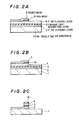
- a stripe-mask 10 of SiO2 having a stripe-width of 2 ⁇ m is formed on the p+-Inp cladding layer 4 to provide an optical waveguide by ordinal photolithography method, and a resist mask 11 is provided on the stripe-mask 10 and on one side of the p+-InP cladding layer 4 relative to the strip-mask 10, as shown in Fig. 2A.
- the p+-InP cladding layer 4 is removed on the other side having no resist mask to provide a thinned p+-InP cladding layer 4 having a thickness of 0.5 ⁇ m by etching, as shown in Fig. 2B.
- the resist mask 11 is removed, and etching is carried out to provide a three-dimensional optical waveguide by use of the SiO2 stripe-mask 10.
- a depth of the etching is controlled to be approximately 1.6 ⁇ m, so that the n-InP cladding layer 2 is exposed on one side of the stripe-mask 10, and the semi-insulating InP substrate 1 is exposed on the other side of the stripe-mask 10, as shown in Fig. 2C.
- the SiO2 stripe-mask 10 is used for a selective epitaxial mask to bury the stripe-mesa portion with Fe-doped semi-insulating InP burying layers 5 on the both sides of the stripe-mesa portion, as shown in Fig. 2D.
- the SiO2 stripe-mask 10 is removed, and a p-electrode 6 is provided on the semi-insulating InP burying layer 5 which is directly in contact with the semi-insulating InP substrate 1. Finally, the semi-insulating InP burying layer 5 which is in contact with the n+-InP cladding layer 2 is etched to expose the n+-InP buffer layer 2, and an n-electrode 7 is provided on the exposed n+-InP cladding layer 2, as shown in Fig. 2E.
- a distance between the p-and n-electrodes 6 and 7 is approximately 100 ⁇ m
- the substrate 1 is polished to be approximately 100 ⁇ m in thickness
- a device length is made to be 1 00 ⁇ m by cleaved facets.
- the p-electrode 6 has an area of 100 ⁇ m x 2 ⁇ m on the stripe-mesa portion, that of 10 ⁇ m x 20 ⁇ m on the interconnection portion, and that of 100 ⁇ m x 100 ⁇ m on the bonding pad portion, such that a capacitance is decreased due to the decrease of a total area based on the separation of the above three portions.
- a static characteristic of the optical modulator will be first explained.
- a wavelength of the incident light 8 is 1.55 ⁇ m used for optical communication.
- the incident light 8 supplied to the optical modulator is supplied therefrom as the output light 9 without any modulation.
- a loss of light transmitted through the optical modulator is as low as approximately 1.5 dB in accordance with the parameters that the device length is 100 ⁇ m, and a wavelength detuning between the incident light 8 and a bandgap of the optical waveguide layer is 75 ⁇ m.
- the junction capacity Cj is 74 fF
- the interconnection and pad capacitances Ci and Cp are totally 12 fF.
- the total device capacitance is 86 fF.
- a device capacitance determining a modulation speed becomes one-fifth to tenth as compared to that of the conventional optical modulator. Consequently, the modulation frequency bandwidth ⁇ f of 74 GHz is obtained to provide an optical modulation having an ultra high speed modulation property.
- Fig. 3 shows an optical modulator in the second preferred embodiment according to the invention. The fabrication steps of this optical modulator will be explained in Figs. 4A to 4D.
- An n+-InP cladding layer 22 having a thickness of 1.0 ⁇ m, an i-InGaAsP light absorption layer 23 having a bandgap wavelength of 1.475 ⁇ m and a thickness of 0.3 ⁇ m, and a p+-InP cladding layer 24 having a thickness of 1.2 ⁇ m are successively grown on a semi-insulating InP substrate 21 by MOVPE method, and a stripe-mask 31 of SiO2 having a width of 2 ⁇ m is formed on the p+-InP cladding layer 24 to provide an optical waveguide by ordinal photolithography method.
- a three-dimensional optical waveguide is provided by etching using the SiO2 stripe-mask 31, as shown in Fig. 4A.
- a depth of the etching is approximately 1.8 ⁇ m, so that the n+-InP cladding layer 22 is exposed.
- the stripe-mesa structure is buried on the both sides with semi-insulating InP burying layers 25 by use of the SiO2 stripe-mask 31. Then, the SiO2 is removed, and a stripe-mask 32 of SiO2 having a width of 20 ⁇ m is provided to cover the stripe-mesa.
- the semi-insulating InP burying layers 25 and a small upper skin portion of the exposed n+-InP cladding layer 22 are etched to provide a relatively wide stripe-mesa structure by use of the SiO2 stripe-mask 32, as shown in Fig. 4B.
- a mask 33 of SiO2 including the SiO2 mask 32 is provided on the relatively wide stripe-mesa structure and on the n+-InP cladding layer 22, such that one side of the cladding layer 22 is covered with the mask 33, and the other side thereof is exposed. Then, the other side of the cladding layer 22 is etched by use of the SiO2 mask 33, as shown in Fig. 4C.
- the SiO2 mask 33 is removed, and a p-electrode 26 is provided on the exposed p+-InP cladding layer 24 of the stripe-mesa structure, and on the semi-insulating burying layer 25 and the semi-insulating InP substance 21 of the side having no n+-InP cladding layer 22 via a passivation film 28 of SiO2. Finally, an n-electrode 27 is provided on the n+-InP cladding layer 22 which is on the side opposite to the p-electrode 26, as shown in Fig. 4D.
- the p-electrode 26 has a stripe-portion 26A, an interconnection portion 26B, and a bondingpad portion 26c, as shown in Fig. 3.
- the semi-insulating InP substrate 21 is polished to be approximately 100 ⁇ m in thickness, and a device length is made to be 100 ⁇ m by cleaved facets.
- the p-electrode 26 has an area of 100 ⁇ m x 2 ⁇ m on the stripe-mesa portion, that of 10 ⁇ m x 20 ⁇ m on the interconnection portion, and that of 100 ⁇ m x 100 ⁇ m on the pad portion.
- the same static characteristic as in the first preferred embodiment is obtained, because the composition and the layer thickness of the i-InGaAsP light absorption layer 23 are the same as those in the first preferred embodiment. That is, a transmission loss between an incident light 29 having a wavelength of 1.55 ⁇ m and an output light 30 is as low as approximately 1.5 dB, and a light extinction ratio is more than 10 dB, when a reverse bias voltage of -3V is applied across the p-and n-electrodes 26 and 27.
- a modulation frequency bandwidth ⁇ f of 69 GHz which is a little narrower than the value in the first preferred embodiment is obtained, because the device capacitance is increased to be 92 fF to a small extent as compared to the value in the first preferred embodiment due to the structure difference of the interconnection and the pad portions of the p-electrode 26.
- This difference can be compensated by changing a polishing thickness of a substrate and/or an area of an electrode bonding pad portion. Consequently, an ultra-high speed optical modulator having a modulation frequency band of more than 50 GHz is easily obtained even in the second preferred embodiment.
- a device length, an optical waveguide width, an electrode bonding pad portion area, etc. may be changed.
- An n-side cladding layer may be composed of an InP layer and an InGaAsP layer, one layer of which is used for an etching-stop layer, and an InGaAsP cap layer may be provided on a p-side InP cladding layer.
- the semi-insulating InP burying layers provided on the both sides of the stripe-mesa structure may be replaced to provide the same advantage for an optical modulator by dielectric material layers such as polyimide, etc.
- Figs. 5A to 5C show an integrated type optical modulator in the first preferred embodiment according to the invention, wherein Fig. 5A is a cross-sectional view along a direction of light transmission, and Figs. 5B and 5C are cross-sectional views along lines B-B and C-C in Fig. 5A, respectively.
- An n+-InGaAsP cladding layer 42 having a bandgap wavelength of 1.2 ⁇ m and a thickness of 0.5 ⁇ m, and an i-InGaAsP active layer having a bandgap wavelength of 1.55 m and a thickness of 0.3 ⁇ m are grown on a semi-insulating InP substrate 41 having a grating 41 A at a region of a semiconductor laser by MOVPE method, and the i-InGaAsP active layer 42 is left only on the grating to expose the n+-InGaAsP cladding layer 42 on a region of an optical modulator having no grating by etching using a SiO2 mask (not shown).
- an i-InGaAsP light absorption layer 44 having a bandgap wavelength of 1.475 ⁇ m and a thickness of 0.3 ⁇ m is selectively grown on the exposed n+-InGaAsP cladding layer 42.
- an optical cascaded connection is obtained between the i-InGaAsP active layer 43 and the i-InGaAsP light absorption layer 44.
- the SiO2 mask is removed, and a p+-InP cladding layer 45 having a thickness of 1.3 ⁇ m is grown on the cascaded connection layer.
- a stripe-mesa structure is formed by two etching steps, such that the semi-insulating InP substrate 41 is exposed on one side of the stripe-mesa structure, and the n+-InGaAsP cladding layer 42 is exposed on the other side of the stripe-mesa structure. Then, the stripe-mesa structure is buried on the both sides with semi-insulating InP burying layers 46, and a groove 52 having a depth of 1 ⁇ m and a length of 10 ⁇ m is provided to provide an electric separation between the optical modulator and the semiconductor laser.
- p-and n-electrodes 47 and 48 for the semiconductor laser, and p- and n-electrodes 49 and 50 for the optical modulator are independently provided, respectively.
- the substrate 41 is polished to be approximately 100 ⁇ m in thickness, and a device length is made to be 400 ⁇ m including 300 ⁇ m for the semiconductor laser and 100 ⁇ m for the optical modulator.
- the p-electrode 49 has an area of 100 ⁇ m x 2 ⁇ m for the stripe-mesa portion, that of 10 ⁇ m x 20 ⁇ m for the interconnection portion, and that of 100 ⁇ m x 100 ⁇ m for the pad portion.
- a forward bias is applied to the laser diode, the stimulated emission occurs, so that a output light 51 is supplied through the light absorption layer 44 which is cascade-connected to the active layer 43.
- a threshold current of the laser diode is 50 mA, a lasing wavelength is 1.55 ⁇ m, and a power of the output light 51 is 5mW, when the current is 100mA.
- a reverse bias voltage -V is applied across the p-and n-electrodes 49 and 50, the light which is propagated through the light absorption layer 44 is absorbed by the Franz-Keldysh effect to provide light modulation. Operation of an optical modulator has been already explained in Fig. 1. Therefore, it is not explained here.
- a modulation frequency bandwidth of more than 50 GHz is obtained to provide an ultra-high speed modulation.
- Materials, a structure and a fabrication method of this integrated type optical modulator may be changed. For instance, an anti-reflection film and a high reflection film are provided on an output facet and a reflection facet, respectively, to provide a high output device.
- the optical modulators as shown in Figs. 1 and 3 may be used as an optical detector.
- the i-InGaAsP light absorption is designed to include a composition having a bandgap of, for instance, 1.67 ⁇ m which is larger than a wavelength of a light source, so that photocurrent induced by light which is absorbed in the light absorption layer is detected by the p- and n-electrodes to realize a waveguide type optical detector.
- a structure and a fabrication process of this optical detector are the same as those explained in Figs. 1 to 4. In this case, a device capacitance is decreased to be as low as 90fF. Consequently, an optical detector having an ultra-wide bandwidth property is obtained.
- Fig. 6 shows an optical modulator in the third preferred embodiment according to the invention.
- This optical modulator is fabricated as shown in Figs. 7A to 7D, and comprises a semi-insulating InP substrate 61, an n-InGaAsP buffer layer 64 having a composition corresponding to a bandgap wavelength of a 1.1 ⁇ m and a thickness of 3 ⁇ m included partially in the upper portion of the substrate 61, a stripe-mesa structure 69 having a width of 1.5 ⁇ m and including an n-InP lower cladding layer 65 having a thickness of 0.5 ⁇ m, an undoped InGaAsP light absorption layer 66 having an thickness of 0.3 ⁇ m and a composition of a 1.4 ⁇ m wavelength, a p-InP upper cladding layer 67 having a thickness of 1.5 ⁇ m and a p+-InGaAs cap layer 68 having a thickness of 0.5 ⁇ m, Fe-doped semi-insulating In
- This optical modulator is fabricated as shown in Figs. 7A to 7D.
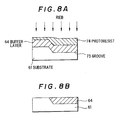
- a stripe-groove 62 having a depth of 3 ⁇ m is formed on a semi-insulatong InP substrate 61 by chemical etching using an etching mask 63 of SiO2, and the groove 62 is buried to be flat relative to the substrate 61 with an n-InGaAsP buffer layer 64 selectively by hydride VPE method.
- etching mask 63 is removed, and an n-InP lower cladding layer 65,an undoped i-InGaAsP light absorption layer 66, a p-InP upper cladding layer 67, and a p+-InGaAs cap layer 68 are grown on the substrate 61 buried with the buffer layer 64 by MO-VPE method.
- a stripe-mesa structure 69 is formed to be positioned over the edge of the stripe-buffer layer 64 by photolithography and etching, such that a width of the stripe-mesa structure 69 is 1.5 ⁇ m, and the high-resistance substrate 61 is exposed on one side, while the buffer layer 64 is exposed on the other side. Then, the stripe-mesa structure 69 is buried on the both sides with Fe-doped semi-insulating InP burying layers 70.
- a portion of the semi-insulating layer 70 which is positioned on the buffer layer 64 is removed by use of etchant of,for instance, HCl for etching only InP selectively.
- etchant for instance, HCl for etching only InP selectively.
- a p-electrode 71 of Ti/Pt/Au is provided on the cap layer 68 and on the semi-insulating burying layer 70 by sputtiring method
- an n-electrode 72 of AuGeNi is provided on the exposed portion of the buffer layer 64 by thermal VDE method.
- anti-reflection films of SiNx are provided on both cleaved facets of the device by sputtering method.
- the optical modulator thus fabricated has a device capacitance of 0.25pF, and a modulation frequency bandwidth of 26 GHz is obtained, when an incident light having a wavelength of 1.55 ⁇ m is supplied to the device. These performances are improved as twice as those in the conventional optical modulator.
- InGaAsP may be replaced in the buffer layer 64 by n-InP.
- the semi-insulating substrate 61 and the buffer layer 64 are exposed on the both sides of the stripe-mesa structure 69 by only one mesa etching step, and photolithography is easily carried out at the time of the mesa etching. As a result, yield and uniformity are improved as twice as those in the conventional optical modulator.
- Figs. 8A and 8B, 9A and 9B, and 10A and 10B show methods for providing a semi-insulating substance having a flat surface and a stripe-buffer layer of a first conduction type provided partially in the upper portion of the substrate.
- a groove 73 having a depth of 3 ⁇ m is formed on a semi-insulating substrate 61 which is then covered on its entire surface by a buffer layer 64 of n-InGaAsP having a thickness of approximately 3 ⁇ m. Thereafter, a photoresist 74 (for instance, AZ-series of Hexist Inc.) is applied on the n-InGaAsP buffer layer 64 to provide a substantially flat surface by spin-coating.
- a photoresist 74 for instance, AZ-series of Hexist Inc.
- the photoresist 74 and the buffer layer 64 are etched at an uniform velocity by RIBE (reactive ion beam etching).
- This uniform velocity etching is realized by adjusting a mixing ratio of mixture gas consisting of Ar, O2 and HCl which is used as reactive gas for the etching.
- the etching is finished. If residual photoresist exists on the buffer layer 64, the photoresist is removed.
- the substrate thus obtained is easy to be controlled in following fabrication steps to provide better yield and interlayer-uniforminity, because the flatness degree of the surface is high.
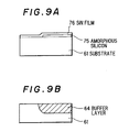
- an amorphous Si layer 75 is formed partially on a semi-inslating substrate 61.
- the semi-insulating substrate 61 having the amorphous Si layer 75 is then covered by a SiN film 76.
- a thermal treatment is carried out at a temperature of approximately 800°C to diffuse Si into the substrate 61. Then, the SiN film 76 and the amorphous Si layer 75 are removed. The surface of the substrate thus obtained is completely flat, so that the formation of a stripe-mesa structure becomes much easy. Further, the fabrication of a diffraction grating necessary for the integration with DFB laser, etc. becomes easy.
- the n-buffer layer 64 may be replaced by a p-buffer layer.
- impurities such as Zn, Cd, etc. are diffused into the semi-insulating substrate. In this case, the conduction types of the other semiconductor layers are necessary to be reverse.
- an n-InP buffer layer 64 having a thickness of approximately 3 ⁇ m is provided on the entire surface of a semi-insulating substrate 61.
- ions such as H+, B+, etc. for increasing a resistance of a semiconductor are injected at a region having no necessity of the provision of a buffer layer into the semi-insulating substrate 61 by a depth of more than a thickness of the buffer layer 64.
- the n-buffer layer 64 is partially formed in the upper portion of the substrate 61.
- a thickness of the buffer layer 64 can be larger than those obtained in Figs. 8B and 9B, because ion such as H+ and B+ is injected deeper than Si+. This provides a large freedom in designing a buffer layer.
- Fig. 11 shows an optical modulator in the fourth preferred embodiment according to the invention
- Figs. 12A to 12C show the fabrication method of the optical modulator.
- the optical modulator comprises a semi-insulating InP substrate 101, a stripe-mesa structure 106 including an n+-InP cladding layer 102, an i-InGaAsP light absorption layer 103, a p-InP cladding layer 104, and a p+-InGaAs cap layer 105, semi-insulating InP burying layers 107 provided on the both sides of the stripe-mesa structure 106, a p-electrode 108, an n-electrode 109, a dielectric layer 110, and a beneath layer electrode 112.
- the p-electrode 108 has a stripe-portn 121, an interconnection portion 114 of an air-bridge structure, and a bonding pad 115A, and the n-electrode 109 has a bonding pad 115B.
- MOVPE organic metal vapour phase epitaxy
- a stripe-SiO2 mask having a width of 2 ⁇ m is provided on the cap layer 105 by ordinal photolithography method, and a stripe-mesa structure 106 is formed to expose the cladding layer 102 by etching using the stripe-SiO2 mask. Then, this stripe-SiO2 mask is used for selectively burying the stripe-mesa structure on the both sides with Fe-doped semi-insulating InP burying layers 107.
- a stripe-mesa structure having a width of 10 ⁇ m including the stripe-mesa structure 106 and the burying layers 107 is formed to expose the cladding layer 102 on one side and the high-resistance InP substrate 101 on the other side by selective etching using ordinal photolithography method.
- a p-electrode 108 of AuZn is provided on the cap layer 105, and an n-electrode 109 of AuGeNi is provided on the cladding layer 102, respectively, as shown in 12A.
- a lower resist 111 having a thickness of 2 ⁇ m is patterned to provide air-gap for the air-bridge interconnection stuructre, and a beneath layer electrode 112 of Ti/Au having respective thicknesses 500 ⁇ /500 ⁇ , on which an Au-plating electrode is provided, is provided by vapor deposition in vacuum. Then, an upper resist 113 which is patterned on the beneath layer electrode 112 is used for a mask, so that a selective Au-plating layer 120 is provided, as shown in Fig. 12B.
- the upper resist 113 is removed by O2 plasma, and a predetermined portion of the beneath layer electrode 112 is removed.
- the lower resist 111 is removed to provide an interconnection part 114 for the air-bridge structure and a bonding pad 115, as shown in 12C.
- the semi-insulating InP substrate 101 is polished to be approximately 100 ⁇ m in thickness, and a length of the devide is made to be 100 ⁇ m by cleaved facets.
- the p-electrode has an area of 100 ⁇ m x 2 ⁇ m at the stripe-portion 121, and that of 50 ⁇ m x 50 ⁇ m at the pad portion 115, and the interconnection portion 114 has a width of 10 ⁇ m, a length of 50 ⁇ m, and a height of 2 ⁇ m at the air-bridge structure.
- a static characteristic In operation of this optical modulator, a static characteristic will be first discussed. Here, it is assumed that a wavelength of an incident light is 1.55 ⁇ m used for optical communication. When no reverse bias voltage is applied across the p- and n-electrodes 108 and 109, the incident light is transmitted through the device as an output light without any modulation. In this case, a transmission loss is as low as approximately 1.5dB, because a wavelength detuning between the incident light and the bandgap of the light absorption layer is 75 ⁇ m.
- a reverse bias voltage is applied across the p-and n-electrodes 108 and 109 to apply an electric field to the i-InGaAsP light absorption layer 103, an incident light is absorbed in the i-InGaAsP light absorption layer 103 during the transmission through the device by Franz-Keldysh effect, so that no output light is supplied therefrom.
- a light extinction ratio is more than 10 dB which is a satisfactory property by a voltage of -3V.
- a frequency bandwidth ⁇ f of an optical modulator using a field effect is determined by a device capacitance C, as defined below.
- ⁇ f 1/( ⁇ CR)
- a jenction capacitance C j is 74fF
- an interconnection capacitance C i and a pad capacitance C p are tolally 3fF.
- a total capacitance of this device determining a modulation speed is 77fF which is one fifth to nineth as compared to the conventional optical modulator, and a modulation frequency bandwidth of 83 GHz is obtained to provide an optical modulator having an ultra-high speed modulation property.
- Fig. 13 shows an optical detector in a preferred embodiment according to the invention. Parts of this optical detector is indicated by like referrence numerals as used in Fig. 11. The only difference therebetween is that the light absoprtion layer 116 is composed of InGaAs having a lattice matching property relative to InP. The same fabrication method as shown in Figs. 12A to 12C is adopted to fabricate this optical detector.
- this optical detector when a wavelength of an incident light is 1.55 ⁇ m, the incident light is effectively absorbed in the light absorption layer 116 of InGaAs, because a bandgap wavelength of the light absorption layer 116 is 1.67 ⁇ m which is on a wavelength side longer than that of the incident light. Photocurrent induced by absorbed light is detected by the p-and n-electrodes 108 and 109. Thus, this device functions as a waveguide type optical detector.
- a device capacitance can be less than 0.1 pF to provide an optical detector having an ultra-wide bandwidth property.
- n-and p-layers may be replaced by opposite conduction type layers, respectively.
- the light absorption layer may be replaced by a multi-quantum well structure.
- Materials are not limited to InGaAsP/InP, but materials such as InGaAs/InAlAs, AlGaAs/GaAs, AlGaInP/GaInP/GaAs, etc. which are used in ordinal semiconductor lasers and semiconductor hererojunction detectors may be used.
- the Fe-doped semi-insulating InP layer may be replaced by a semi-insulating semiconductor layer doped with dopant such as Co, Ti, etc., or by a semi-insulating dielectric material such as polyimide.
Abstract
Description
- This invention relates to an optical semiconductor device, and more particularly to, an optical semiconductor device applicable to an optical modulator, an integrated type optical modulator, an optical detector, etc.
- In accordance with the development of optical communication systems in recent years, optical modulators which operate at an ultra-high speed and by a low voltage, and are small in size and easily integrated with other devices, optical detectors which operate at a high speed, etc. are highly required to be put into practical use. In optical semiconductor modulators, an optical modulator which utilizes an effect of increasing light absorption loss in an optical waveguide by applying a voltage to the optical waveguide (Franz-Keldysh effect or Quantum confined Stark effect) has advantages in that, if a device capacitance is decreased, it operates with a several tens GHz modulation bandwidth, and it can be integrated with a DFB laser, etc. For instance, a 20 GHz optical modulator using a InGaAlAs/InAlAs multiple quantum well structure is described in "a preliminary lecture paper C-474 of the spring national conference, 1989 in the Institute of Electronics Informations and Communications Engineers" by Wakita et al. This modulator is an absorption type modulator utilizaing the shift of an absorption peak induced by an electric field generated by a reverse bias voltage applied to a semiconductor PIN structure, and comprises an n-InAlAs cladding layer, a multiple quantum well layer and a p-InAlAs cladding layer successively grown on an n-InP substrate by MBE method. A modulation frequency band Δf of this modulator is almost determined by a device capacitance C, and is defined by a below equation.

- The device capacitance C is expressed by a sum of a junction capacitance Cj of a pn junction in the stripe-optical waveguide, an interconnection capacitance Ci of an interconnection connecting a stripe-electrode to a bonding pad, and a pad capacitance Cp at the bonding pad.
- In this modulator, the device capacitance is as low as 0.2pF to provide an ultra-high speed modulation, because it has a structure of a low capacitance having a polyimide burying layer under the bonding pad. Even in this structure, however, the junction capacitance Cj which is inherent to a modulator is less than a half of the whole device capacitance C, and the remaining is the interconnection and pad capacitances Ci and Cp which are unnecessary for the device and is produced among the n-InP substrate, the interconnection, and the electrode. Considering the switching characteristics of this modulator, a large decrease of the junction capacitance Cj is difficult, because this modulator has a device length of approximately 100 µm. In addition, the decrease of the interconnection and pad capacitances Ci and Cp is also difficult, because a conductive substrate such as the n-InP substrate is used.
- For this reason, a conventional optical modulator has a modulation band of 20 to 25 GHz at most, so that it can not be applied to an ultra-high speed optical modulator having a modulation band of more than 50 GHz.
- Another conventional optical modulator is described in "IOOC '89, Technical digest 20PDB-5, 1989" by Soda et al. This optical modulator is integrated with a DFB laser on an n-InP substrate, and is a modulator utilizing light absorption of Franz-Keldysh effect and having burying layers of semi-insulating InP on the both sides of an optical waveguide for the modulator and the DFB laser. Even in this integrated modulator, a polyimide layer is provided under an electrode pad to decrease a large parasitic capacitance, because a large capacitance is generated due to the use of the conductive substrate. As a result, a device capacitance is approximately 0.55pF, and a modulation band is approximately 10 GHz.
- As described above, a limitation occurs in decreasing a device capacitance, because a conductive substrate is used. A limitation also occurs in expanding a modulation frequency bandwidth, as explained to be approximately 25 GHz in the former modulator and approximately 10 GHz in the latter integrated type modulator, because a thickness of the semi-insulating layer between the electrode provided on the conductive substrate and the other electrode provided on the stripe-mesa portion and the semi-insulating layer is only 2 to 3 µm on the both sides of the stripe-mesa portion, so that it is difficult to decrease the device capacitance to less than 0.5pF. Although the device capacitance is more decreased by increasing the thickness, another limitation occurs in fabricating the devices due to the increase of a mesa height.
- In order to overcome these disadvantages, an absorption type optical modulator using a semi-insulating InP substrate is proposed on pages 270 to 272 of "IEEE PHOTONICS TECHNOLOGY LETTERS,
Vol 1, No.9, September 1989" by Lin et al. This optical modulator comprises a lower undoped InP cladding layer, an undoped InGaAsP absorption layer, an upper undoped InP cladding layer, a p-InP cladding layer, and a p-InGaAsP cap layer successively provided on the semi-insulating InP substrate, and has a ridge type optical waveguide formed by removing portions of the p-InGaAs cap layer, the p-InP cladding layer, and the upper undoped InP cladding layer by etching. The optical modulator further comprises a p-electrode provided on the p-InGaAsP cap layer, and an n-electrode provided on the undoped InGaAsP absorption layer. - In this optical modulator, it is considered that a resistance of the n-side semiconductor layers is large, and a serial resistance of this device is large, although a device capacitance is as low as 10fF, when an electric field is applied to this device. In this case, a disadvantage occurs in that high speed operation is difficult to be realized due to the large resistance, in spite of the small device capacitance.
- Otherwise, if the undoped layers becomes n-layers in this optical modulator, the serial resistance and the expansion of a depletion layer are considered to be deviated in run-to-run operation. Thus, the reproducibility of a modulation frequency bandwidth and an operation voltage is lowered to result in the low practicability.
- Accordingly, it is an object of this invention to provide an optical semiconductor device such as an optical modulator, an integrated type optical modulator, an optical detector, etc. by reducing an interconnection capacitance and a bonding pad capacitance.
- It is a further object of this invention to provide an optical semiconductor device such as an optical modulator, an integrated type optical modulator, an optical detector having a wide bandwidth property and a high practicability.
- According to this invention, an optical semiconductor device, comprises: a stripe-mesa structure provided on a semi-insulating semiconductor substrate, the stripe-mesa structure including at least a first conduction type cladding layer, an undoped light absorption layer, a second conduction type cladding layer, and a second conduction type cap layer; semi-insulating burying layers provided on both sides of the stripe-mesa structure; and means for applying a predetermined electric field to the undoped light absorption layer.
- In this invention, a semi-insulating semiconductor substrate is used, and an optical waveguide of a PIN structure is buried on its both sides with semi-insulating layers, such that a capacitance of portions having no connection with operation of an optical semiconductor device such as an optical modulator, an integrated type optical modulator, an optical detector, etc. is decreased as much as possible to decrease a total capacitance of the device. This provides an optical semiconductor device having a property of a wide bandwidth.
- In general, a capacitance C is expressed by a below equation.

where εs is a specific inductivity, ε o is a dielectric constant of vacuum, S is an area of each electrode (or a pn junction area), and d is a distance between electrodes (or a depletion thickness). As described in the conventional optical modulator, a total capacitance Ct of a device is expressed by a below equation.

where Cj is a junction capacitance, Ci is an interconnection capacitance, and Cp is a bonding pad capacitance. The junction capacitance Cj has an effect on a static characteristic of an optical modulator. Therefore, the optical modulator is designed to provide no deterioration of the static characteristic, such that an optical waveguide width is 2 µm, an optical waveguide length is 100 µm, and a depletion layer thickness is 0.3 µm. Thus, the junction capacitance Cj of approximately 74 fF is obtained. The interconnection and pad capacitances Ci and Cp are desired to be decreased for a wide bandwidth property of the optical modulator. - In this invention, the distance a between the electrodes is as long as approximately 100 µm, so that the interconnection and pad capacitances Ci and Cp are decreased to be one-tenth of those in the conventional optical modulator using a conductive substrate and a dielectric burying layer such as polyimide, etc. provided only under a bonding pad (d is 2 to 3 µm and εs is equal to or nearly 3), and one-thirtyth of those in the conventional optical modulator using a semi-insulating burying layer of a semiconductor provided only under a bonding pad (d is 2 to 3 µm, and ε₃ is equal to or nearly 12). Consequently, the total capacitance Ct of the device is determined almost by the junction capacitance Cj, so that an optical semiconductor device having a wide bandwidth property is obtained.
- An optical waveguide of a PIN structure provided on asemi-insulating substrate and buried with semi-insulating layers is similar in structure to a semiconductor laser. Therefore, an optical modulator according to the invention is easily integrated with a semiconductor laser to provide an integrated type optical modulator operating at an ultra-high speed.
- A structure of an optical modulator according to the invention can be used as a waveguide type optical detector, if a light absorption layer is composed of a material having a bandgap wavelength which is longer than a wavelength of a light source, and photocurrent induced by light absorbed in the light absorption layer is detected by p-and n-electrodes.
- This invention will be explained in more detail in conjunction with appended drawings, wherein:
- Fig. 1 is a schematic view of an optical modulator in a first preferred embodiment according to the invention;
- Figs. 2A to 2E are schematic cross-sectional views showing steps of fabricating the optical modulator in the first preferred embodiment;
- Fig. 3 is a schematic view of an optical modulator in a second preferred embodiment according to the invention;
- Figs. 4A to 4D are schematic cross-sectional views showing steps of fabricating the optical modulator in the second preferred embodiment;
- Figs. 5A to 5C are schematic cross-sectional views showing an integrated type optical modulator in a first preferred embodiment according to the invention;
- Fig. 6 is a schematic view showing an optical modulator in a third preferred embodiment according to the invention;
- Figs. 7A to 7C are schematic cross-sectional views showing steps of fabricating the optical modulator in the third preferred embodiment;
- Figs. 8A and 8B, 9A and 9B, and 10A and 10B are schematic cross-sectional views showing steps of fabricating semi-insulating substrates having buffer layers of a first conduction type;
- Fig. 11 is a schematic view showing an optical modulator in a fourth preferred embodiment according to the invention;
- Figs 12A to 12C are schematic cross-sectional views showing steps of fabricating the optical modulator in the fourth preferred embodiment; and
- Fig. 13 is a schematic view showing an optical detector in a first preferred embodiment according to the invention.
- Fig. 1 shows an optical modulator in the first preferred embodiment according to the invention. The optical modulator comprises a
semi-insulating InP substrate 1, an n⁺-InP cladding layer 2, an i-InGaAslight absorption layer 3, a p⁺-InP cladding layer 4, semi-insulatingInP burying layers 5, a p-electrode 6, and an n-electrode 7. The p-electrode 6 has astripe porion 6A, aninterconnection portion 6B, and abonding pad portion 6C. - In this optical modulator, an
incident light 8 is modulated to be supplied as anoutput light 9 dependent on a light absorption coefficient changing based on an electric field generated by a voltage -V applied across the p- and n-electrodes - In the optical modulator of the first preferred embodiment, though an optical waveguide of a double-hetero structure using a InGaAsP/InP system material is explained, the material and the structure may be replaced by an InGaAs/InAlAs system material, a GaAs/AlGaAs system material, etc. and by a multiple quantum well structure, etc.
- The fabrication steps of the optical modulator will be explained in Figs. 2A to 2E.
- An n⁺-
InP cladding layer 2 having a thickness of 0.5 µm, an i-InGaAsPlight absorption layer 3 having a bandgap wavelength of 1.475 µm and a thickness of 0.3 µm, and a p⁺-Inp cladding layer 4 having a thickness of 1.2 µm are successively grown on asemi-insulating InP substrate 1 by MOVPE method. Then, a stripe-mask 10 of SiO₂ having a stripe-width of 2 µm is formed on the p⁺-Inp cladding layer 4 to provide an optical waveguide by ordinal photolithography method, and a resistmask 11 is provided on the stripe-mask 10 and on one side of the p⁺-InP cladding layer 4 relative to the strip-mask 10, as shown in Fig. 2A. - The p⁺-
InP cladding layer 4 is removed on the other side having no resist mask to provide a thinned p⁺-InP cladding layer 4 having a thickness of 0.5µ m by etching, as shown in Fig. 2B. - The resist
mask 11 is removed, and etching is carried out to provide a three-dimensional optical waveguide by use of the SiO₂ stripe-mask 10. At this time, a depth of the etching is controlled to be approximately 1.6 µm, so that the n-InP cladding layer 2 is exposed on one side of the stripe-mask 10, and thesemi-insulating InP substrate 1 is exposed on the other side of the stripe-mask 10, as shown in Fig. 2C. - The SiO₂ stripe-
mask 10 is used for a selective epitaxial mask to bury the stripe-mesa portion with Fe-doped semi-insulatingInP burying layers 5 on the both sides of the stripe-mesa portion, as shown in Fig. 2D. - The SiO₂ stripe-
mask 10 is removed, and a p-electrode 6 is provided on the semi-insulatingInP burying layer 5 which is directly in contact with thesemi-insulating InP substrate 1. Finally, the semi-insulatingInP burying layer 5 which is in contact with the n⁺-InP cladding layer 2 is etched to expose the n⁺-InP buffer layer 2, and an n-electrode 7 is provided on the exposed n⁺-InP cladding layer 2, as shown in Fig. 2E. - In the optical modulator thus fabricated, a distance between the p-and n-
electrodes substrate 1 is polished to be approximately 100 µm in thickness, and a device length is made to be 1 00 µm by cleaved facets. The p-electrode 6 has an area of 100 µm x 2 µm on the stripe-mesa portion, that of 10 µm x 20 µm on the interconnection portion, and that of 100 µm x 100 µm on the bonding pad portion, such that a capacitance is decreased due to the decrease of a total area based on the separation of the above three portions. - In operation, a static characteristic of the optical modulator will be first explained. Here, it is assumed that a wavelength of the
incident light 8 is 1.55µm used for optical communication. When no reverse bias voltage is applied across the p- and n-electrodes incident light 8 supplied to the optical modulator is supplied therefrom as theoutput light 9 without any modulation. In this case, a loss of light transmitted through the optical modulator is as low as approximately 1.5 dB in accordance with the parameters that the device length is 100 µm, and a wavelength detuning between theincident light 8 and a bandgap of the optical waveguide layer is 75 µm. When an electric field is applied to the i-InGaAsPlight absorption layer 3 by applying a reverse bias voltage - V across the p- and n-electrodes output light 9 is obtained, because the light is absorbed in the i- InGaAsPlight absorption layer 3 by Franz-Keldysh effect. In this case, a satisfactory result that a light extinction ratio is more than 10 dB is obtained, when the reverse bias voltage is -3V. - Next, a modulation characteristic will be explained. As described before, the modulation frequency bandwidth Δf is determined by the below equation.

- In this preferred embodiment, if it is assumed that a specific inductivity of a semiconductor is 12.5, the junction capacity Cj is 74 fF, and the interconnection and pad capacitances Ci and Cp are totally 12 fF. Thus, the total device capacitance is 86 fF. As a result, a device capacitance determining a modulation speed becomes one-fifth to tenth as compared to that of the conventional optical modulator. Consequently, the modulation frequency bandwidth Δf of 74 GHz is obtained to provide an optical modulation having an ultra high speed modulation property.
- Fig. 3 shows an optical modulator in the second preferred embodiment according to the invention. The fabrication steps of this optical modulator will be explained in Figs. 4A to 4D.
- An n⁺-
InP cladding layer 22 having a thickness of 1.0 µm, an i-InGaAsPlight absorption layer 23 having a bandgap wavelength of 1.475µ m and a thickness of 0.3 µm, and a p⁺-InP cladding layer 24 having a thickness of 1.2 µm are successively grown on asemi-insulating InP substrate 21 by MOVPE method, and a stripe-mask 31 of SiO₂ having a width of 2 µm is formed on the p⁺-InP cladding layer 24 to provide an optical waveguide by ordinal photolithography method. Then, a three-dimensional optical waveguide is provided by etching using the SiO₂ stripe-mask 31, as shown in Fig. 4A. At this time, a depth of the etching is approximately 1.8µm, so that the n⁺-InP cladding layer 22 is exposed. - The stripe-mesa structure is buried on the both sides with semi-insulating
InP burying layers 25 by use of the SiO₂ stripe-mask 31. Then, the SiO₂ is removed, and a stripe-mask 32 of SiO₂ having a width of 20 µm is provided to cover the stripe-mesa. The semi-insulatingInP burying layers 25 and a small upper skin portion of the exposed n⁺-InP cladding layer 22 are etched to provide a relatively wide stripe-mesa structure by use of the SiO₂ stripe-mask 32, as shown in Fig. 4B. - A
mask 33 of SiO₂ including theSiO₂ mask 32 is provided on the relatively wide stripe-mesa structure and on the n⁺-InP cladding layer 22, such that one side of thecladding layer 22 is covered with themask 33, and the other side thereof is exposed. Then, the other side of thecladding layer 22 is etched by use of theSiO₂ mask 33, as shown in Fig. 4C. - The
SiO₂ mask 33 is removed, and a p-electrode 26 is provided on the exposed p⁺-InP cladding layer 24 of the stripe-mesa structure, and on thesemi-insulating burying layer 25 and thesemi-insulating InP substance 21 of the side having no n⁺-InP cladding layer 22 via apassivation film 28 of SiO₂. Finally, an n-electrode 27 is provided on the n⁺-InP cladding layer 22 which is on the side opposite to the p-electrode 26, as shown in Fig. 4D. The p-electrode 26 has a stripe-portion 26A, an interconnection portion 26B, and a bondingpad portion 26c, as shown in Fig. 3. - In the optical modulator thus fabricated, the
semi-insulating InP substrate 21 is polished to be approximately 100 µm in thickness, and a device length is made to be 100 µm by cleaved facets. The p-electrode 26 has an area of 100 µm x 2 µm on the stripe-mesa portion, that of 10 µm x 20 µm on the interconnection portion, and that of 100 µm x 100 µm on the pad portion. - In operation of the optical modulator in the second preferred embodiment, the same static characteristic as in the first preferred embodiment is obtained, because the composition and the layer thickness of the i-InGaAsP
light absorption layer 23 are the same as those in the first preferred embodiment. That is, a transmission loss between anincident light 29 having a wavelength of 1.55 µm and anoutput light 30 is as low as approximately 1.5 dB, and a light extinction ratio is more than 10 dB, when a reverse bias voltage of -3V is applied across the p-and n-electrodes - On the other hand, a modulation frequency bandwidth Δf of 69 GHz which is a little narrower than the value in the first preferred embodiment is obtained, because the device capacitance is increased to be 92 fF to a small extent as compared to the value in the first preferred embodiment due to the structure difference of the interconnection and the pad portions of the p-
electrode 26. This difference can be compensated by changing a polishing thickness of a substrate and/or an area of an electrode bonding pad portion. Consequently, an ultra-high speed optical modulator having a modulation frequency band of more than 50 GHz is easily obtained even in the second preferred embodiment. - In the optical modulators of the first and second preferred embodiments, a device length, an optical waveguide width, an electrode bonding pad portion area, etc. may be changed. An n-side cladding layer may be composed of an InP layer and an InGaAsP layer, one layer of which is used for an etching-stop layer, and an InGaAsP cap layer may be provided on a p-side InP cladding layer. Further, the semi-insulating InP burying layers provided on the both sides of the stripe-mesa structure may be replaced to provide the same advantage for an optical modulator by dielectric material layers such as polyimide, etc.
- Figs. 5A to 5C show an integrated type optical modulator in the first preferred embodiment according to the invention, wherein Fig. 5A is a cross-sectional view along a direction of light transmission, and Figs. 5B and 5C are cross-sectional views along lines B-B and C-C in Fig. 5A, respectively.
- First, the fabrication steps of this integrated type optical modulator will be briefly explained.
- An n⁺-
InGaAsP cladding layer 42 having a bandgap wavelength of 1.2 µm and a thickness of 0.5 µm, and an i-InGaAsP active layer having a bandgap wavelength of 1.55 m and a thickness of 0.3 µm are grown on asemi-insulating InP substrate 41 having a grating 41 A at a region of a semiconductor laser by MOVPE method, and the i-InGaAsPactive layer 42 is left only on the grating to expose the n⁺-InGaAsP cladding layer 42 on a region of an optical modulator having no grating by etching using a SiO₂ mask (not shown). Then, an i-InGaAsPlight absorption layer 44 having a bandgap wavelength of 1.475 µm and a thickness of 0.3 µm is selectively grown on the exposed n⁺-InGaAsP cladding layer 42. As a result, an optical cascaded connection is obtained between the i-InGaAsPactive layer 43 and the i-InGaAsPlight absorption layer 44. Then, the SiO₂ mask is removed, and a p⁺-InP cladding layer 45 having a thickness of 1.3µm is grown on the cascaded connection layer. The steps as explained in Figs. 2A to 2D are applied to the fabrication process after the above steps in this preferred embodiment. That is, a stripe-mesa structure is formed by two etching steps, such that thesemi-insulating InP substrate 41 is exposed on one side of the stripe-mesa structure, and the n⁺-InGaAsP cladding layer 42 is exposed on the other side of the stripe-mesa structure. Then, the stripe-mesa structure is buried on the both sides with semi-insulatingInP burying layers 46, and agroove 52 having a depth of 1 µm and a length of 10µ m is provided to provide an electric separation between the optical modulator and the semiconductor laser. Finally, p-and n-electrodes electrodes substrate 41 is polished to be approximately 100 µm in thickness, and a device length is made to be 400 µ m including 300 µm for the semiconductor laser and 100 µm for the optical modulator. The p-electrode 49 has an area of 100 µm x 2 µm for the stripe-mesa portion, that of 10 µm x 20 µm for the interconnection portion, and that of 100 µm x 100 µm for the pad portion. - In operation, when a forward bias is applied to the laser diode, the stimulated emission occurs, so that a
output light 51 is supplied through thelight absorption layer 44 which is cascade-connected to theactive layer 43. A threshold current of the laser diode is 50 mA, a lasing wavelength is 1.55 µm, and a power of theoutput light 51 is 5mW, when the current is 100mA. When a reverse bias voltage -V is applied across the p-and n-electrodes light absorption layer 44 is absorbed by the Franz-Keldysh effect to provide light modulation. Operation of an optical modulator has been already explained in Fig. 1. Therefore, it is not explained here. Even in this integrated type optical modulator, a modulation frequency bandwidth of more than 50 GHz is obtained to provide an ultra-high speed modulation. Materials, a structure and a fabrication method of this integrated type optical modulator may be changed. For instance, an anti-reflection film and a high reflection film are provided on an output facet and a reflection facet, respectively, to provide a high output device. - The optical modulators as shown in Figs. 1 and 3 may be used as an optical detector. In such an application, the i-InGaAsP light absorption is designed to include a composition having a bandgap of, for instance, 1.67 µm which is larger than a wavelength of a light source, so that photocurrent induced by light which is absorbed in the light absorption layer is detected by the p- and n-electrodes to realize a waveguide type optical detector. A structure and a fabrication process of this optical detector are the same as those explained in Figs. 1 to 4. In this case, a device capacitance is decreased to be as low as 90fF. Consequently, an optical detector having an ultra-wide bandwidth property is obtained.
- Fig. 6 shows an optical modulator in the third preferred embodiment according to the invention. This optical modulator is fabricated as shown in Figs. 7A to 7D, and comprises a
semi-insulating InP substrate 61, an n-InGaAsP buffer layer 64 having a composition corresponding to a bandgap wavelength of a 1.1 µm and a thickness of 3 µm included partially in the upper portion of thesubstrate 61, a stripe-mesa structure 69 having a width of 1.5 µm and including an n-InPlower cladding layer 65 having a thickness of 0.5 µm, an undoped InGaAsPlight absorption layer 66 having an thickness of 0.3 µm and a composition of a 1.4 µm wavelength, a p-InPupper cladding layer 67 having a thickness of 1.5 µm and a p⁺-InGaAs cap layer 68 having a thickness of 0.5 µm, Fe-doped semi-insulatingInP burying layers 70 provided on the both sides of themesa structure 69 thereby buried, a p-electrode 71 provided on thesemi-insulating layer 70 and on themesa structure 69, and an n-electrode 72 provided on the exposed portion of thebuffer layer 64. Anti-reflection films are provided on both facets corresponding to light input and output planes to suppress light reflection thereon, and a device length is 300µm. - This optical modulator is fabricated as shown in Figs. 7A to 7D.
- In Fig. 7A, a stripe-
groove 62 having a depth of 3 µm is formed on asemi-insulatong InP substrate 61 by chemical etching using anetching mask 63 of SiO₂, and thegroove 62 is buried to be flat relative to thesubstrate 61 with an n-InGaAsP buffer layer 64 selectively by hydride VPE method. - In Fig. 7B, the
etching mask 63 is removed, and an n-InPlower cladding layer 65,an undoped i-InGaAsPlight absorption layer 66, a p-InPupper cladding layer 67, and a p⁺-InGaAs cap layer 68 are grown on thesubstrate 61 buried with thebuffer layer 64 by MO-VPE method. - In Fig. 7C, a stripe-
mesa structure 69 is formed to be positioned over the edge of the stripe-buffer layer 64 by photolithography and etching, such that a width of the stripe-mesa structure 69 is 1.5 µm, and the high-resistance substrate 61 is exposed on one side, while thebuffer layer 64 is exposed on the other side. Then, the stripe-mesa structure 69 is buried on the both sides with Fe-doped semi-insulating InP burying layers 70. - In Fig. 7D, a portion of the
semi-insulating layer 70 which is positioned on thebuffer layer 64 is removed by use of etchant of,for instance, HCℓ for etching only InP selectively. Then, a p-electrode 71 of Ti/Pt/Au is provided on thecap layer 68 and on thesemi-insulating burying layer 70 by sputtiring method, and an n-electrode 72 of AuGeNi is provided on the exposed portion of thebuffer layer 64 by thermal VDE method. Finally, anti-reflection films of SiNx are provided on both cleaved facets of the device by sputtering method. - The optical modulator thus fabricated has a device capacitance of 0.25pF, and a modulation frequency bandwidth of 26 GHz is obtained, when an incident light having a wavelength of 1.55µm is supplied to the device. These performances are improved as twice as those in the conventional optical modulator.
- In this preferred embodiment, InGaAsP may be replaced in the
buffer layer 64 by n-InP. In the above described fabrication method, thesemi-insulating substrate 61 and thebuffer layer 64 are exposed on the both sides of the stripe-mesa structure 69 by only one mesa etching step, and photolithography is easily carried out at the time of the mesa etching. As a result, yield and uniformity are improved as twice as those in the conventional optical modulator. - Figs. 8A and 8B, 9A and 9B, and 10A and 10B show methods for providing a semi-insulating substance having a flat surface and a stripe-buffer layer of a first conduction type provided partially in the upper portion of the substrate.
- In Fig. 8A, a
groove 73 having a depth of 3µm is formed on asemi-insulating substrate 61 which is then covered on its entire surface by abuffer layer 64 of n-InGaAsP having a thickness of approximately 3µm. Thereafter, a photoresist 74 (for instance, AZ-series of Hexist Inc.) is applied on the n-InGaAsP buffer layer 64 to provide a substantially flat surface by spin-coating. - In Fig. 8B, the
photoresist 74 and thebuffer layer 64 are etched at an uniform velocity by RIBE (reactive ion beam etching). This uniform velocity etching is realized by adjusting a mixing ratio of mixture gas consisting of Ar, O₂ and HCl which is used as reactive gas for the etching. When thesemi-insulating substrate 61 is exposed at a region except for thegroove 73, the etching is finished. If residual photoresist exists on thebuffer layer 64, the photoresist is removed. The substrate thus obtained is easy to be controlled in following fabrication steps to provide better yield and interlayer-uniforminity, because the flatness degree of the surface is high. - In Fig. 9A, an amorphous Si layer 75 is formed partially on a
semi-inslating substrate 61. Thesemi-insulating substrate 61 having the amorphous Si layer 75 is then covered by aSiN film 76. - In Fig. 9B, a thermal treatment is carried out at a temperature of approximately 800°C to diffuse Si into the
substrate 61. Then, theSiN film 76 and the amorphous Si layer 75 are removed. The surface of the substrate thus obtained is completely flat, so that the formation of a stripe-mesa structure becomes much easy. Further, the fabrication of a diffraction grating necessary for the integration with DFB laser, etc. becomes easy. In the above embodiment, the n-buffer layer 64 may be replaced by a p-buffer layer. For the p-buffer layer, impurities such as Zn, Cd, etc. are diffused into the semi-insulating substrate. In this case, the conduction types of the other semiconductor layers are necessary to be reverse. - In Fig. 10A, an n-
InP buffer layer 64 having a thickness of approximately 3µm is provided on the entire surface of asemi-insulating substrate 61. - In Fig. 10B, ions such as H⁺, B⁺, etc. for increasing a resistance of a semiconductor are injected at a region having no necessity of the provision of a buffer layer into the
semi-insulating substrate 61 by a depth of more than a thickness of thebuffer layer 64. As a result, the n-buffer layer 64 is partially formed in the upper portion of thesubstrate 61. A thickness of thebuffer layer 64 can be larger than those obtained in Figs. 8B and 9B, because ion such as H⁺ and B⁺ is injected deeper than Si⁺. This provides a large freedom in designing a buffer layer. - Fig. 11 shows an optical modulator in the fourth preferred embodiment according to the invention, and Figs. 12A to 12C show the fabrication method of the optical modulator.
- The optical modulator comprises a
semi-insulating InP substrate 101, a stripe-mesa structure 106 including an n⁺-InP cladding layer 102, an i-InGaAsPlight absorption layer 103, a p-InP cladding layer 104, and a p⁺-InGaAs cap layer 105, semi-insulatingInP burying layers 107 provided on the both sides of the stripe-mesa structure 106, a p-electrode 108, an n-electrode 109, adielectric layer 110, and a beneathlayer electrode 112. The p-electrode 108 has a stripe-portn 121, aninterconnection portion 114 of an air-bridge structure, and abonding pad 115A, and the n-electrode 109 has abonding pad 115B. - In fabricating this optical modulator, an n⁺-
InP cladding layer 102 having a thickness of 2.0µm and a carrier concentration of 5 x 10¹⁷cm⁻³, an undoped InGaAsPlight absorption layer 103 having a thickness of 0.3µm and a bandgap wavelength of 1.475µm, a p⁺-InP cladding layer 104 having a thickness of 2.0µm and a carrier concentration of 5 x 10¹⁷cm⁻³, and a p⁺-InGaAs cap layer 105 having a thickness of 0.3µm and a carrier concentration of 1 x 10¹⁹cm⁻³ are grown successively on a Fe-dopedsemi-insulating InP substrate 101 by organic metal vapour phase epitaxy (MOVPE) method. Next, a stripe-SiO₂ mask having a width of 2µm is provided on thecap layer 105 by ordinal photolithography method, and a stripe-mesa structure 106 is formed to expose thecladding layer 102 by etching using the stripe-SiO₂ mask. Then, this stripe-SiO₂ mask is used for selectively burying the stripe-mesa structure on the both sides with Fe-doped semi-insulating InP burying layers 107. Thereafter, a stripe-mesa structure having a width of 10µm including the stripe-mesa structure 106 and the buryinglayers 107 is formed to expose thecladding layer 102 on one side and the high-resistance InP substrate 101 on the other side by selective etching using ordinal photolithography method. Next, a p-electrode 108 of AuZn is provided on thecap layer 105, and an n-electrode 109 of AuGeNi is provided on thecladding layer 102, respectively, as shown in 12A. - A lower resist 111 having a thickness of 2µm is patterned to provide air-gap for the air-bridge interconnection stuructre, and a beneath
layer electrode 112 of Ti/Au having respective thicknesses 500Å/500Å, on which an Au-plating electrode is provided, is provided by vapor deposition in vacuum. Then, an upper resist 113 which is patterned on the beneathlayer electrode 112 is used for a mask, so that a selective Au-plating layer 120 is provided, as shown in Fig. 12B. - The upper resist 113 is removed by O₂ plasma, and a predetermined portion of the beneath
layer electrode 112 is removed. Thus, the lower resist 111 is removed to provide aninterconnection part 114 for the air-bridge structure and a bonding pad 115, as shown in 12C. Then, thesemi-insulating InP substrate 101 is polished to be approximately 100µm in thickness, and a length of the devide is made to be 100µm by cleaved facets. The p-electrode has an area of 100µm x 2µm at the stripe-portion 121, and that of 50µm x 50µm at the pad portion 115, and theinterconnection portion 114 has a width of 10µm, a length of 50µm, and a height of 2µm at the air-bridge structure. - In operation of this optical modulator, a static characteristic will be first discussed. Here, it is assumed that a wavelength of an incident light is 1.55µm used for optical communication. When no reverse bias voltage is applied across the p- and n-
electrodes - When a reverse bias voltage is applied across the p-and n-
electrodes light absorption layer 103, an incident light is absorbed in the i-InGaAsPlight absorption layer 103 during the transmission through the device by Franz-Keldysh effect, so that no output light is supplied therefrom. In this case, a light extinction ratio is more than 10 dB which is a satisfactory property by a voltage of -3V. - Next, a modulation characteristic will be explained. As described before, a frequency bandwidth Δf of an optical modulator using a field effect is determined by a device capacitance C, as defined below.

- In this preferred embodiment, if a calculation is carried out in the assumption that a specific dielectric coefficient of the semiconductor is 12.5, a jenction capacitance Cj is 74fF, and an interconnection capacitance Ci and a pad capacitance Cp are tolally 3fF. Thus, a total capacitance of this device determining a modulation speed is 77fF which is one fifth to nineth as compared to the conventional optical modulator, and a modulation frequency bandwidth of 83 GHz is obtained to provide an optical modulator having an ultra-high speed modulation property.
- Fig. 13 shows an optical detector in a preferred embodiment according to the invention. Parts of this optical detector is indicated by like referrence numerals as used in Fig. 11. The only difference therebetween is that the
light absoprtion layer 116 is composed of InGaAs having a lattice matching property relative to InP. The same fabrication method as shown in Figs. 12A to 12C is adopted to fabricate this optical detector. - In this optical detector, when a wavelength of an incident light is 1.55µm, the incident light is effectively absorbed in the
light absorption layer 116 of InGaAs, because a bandgap wavelength of thelight absorption layer 116 is 1.67µm which is on a wavelength side longer than that of the incident light. Photocurrent induced by absorbed light is detected by the p-and n-electrodes light absorption layer 116 are the same as those in the aforementiond first preferred embodiment, a device capacitance can be less than 0.1 pF to provide an optical detector having an ultra-wide bandwidth property. - In the preferred embodiments, n-and p-layers may be replaced by opposite conduction type layers, respectively. The light absorption layer may be replaced by a multi-quantum well structure. Materials are not limited to InGaAsP/InP, but materials such as InGaAs/InAlAs, AlGaAs/GaAs, AlGaInP/GaInP/GaAs, etc. which are used in ordinal semiconductor lasers and semiconductor hererojunction detectors may be used. The Fe-doped semi-insulating InP layer may be replaced by a semi-insulating semiconductor layer doped with dopant such as Co, Ti, etc., or by a semi-insulating dielectric material such as polyimide. Although it is considered that stress is applied to a semiconductor layer, because a thermal expansion coefficient of polyimide is different from that of a semiconductor, a predetermined reliability is obtained in accordance with the decrease of stress by decreasing a volume of polyimide as a result of narrowing a width of a groove. Polyimide is effectively used in an optical modulator and an optical detector, although a semiconductor is preferably used in a semiconductor laser which generally produces heat.
- Although the invention has been described with respect to specific embodiment for complete and clear disclosure, the appended claims are not to be thus limited but are to be construed as embodying all modification and alternative constructions that may occur to one skilled in the art which fairly fall within the basic theaching herein set forth.
Claims (17)
- An optical semiconductor device, comprising:
a stripe-mesa structure provided on a semi-insulating substrate, said stripe-mesa structure including a first cladding layer of a first conduction type, an undoped light absorption layer, a second caldding layer of a second conduction type, and a cap layer of said second conduction type;
semi-insulating burying layers for burying said stripe-mesa structure on both sides thereof; and
means for applying an electric field to said undoped light absorption layer. - An optical semiconductor device, according to claim 1, wherein:
said applying means includes a first electrode connected to said cap layer, and a second electrode connected to said first cladding layer exposed on said semi-insulating substrate. - An optical semiconductor device, according to claim 2, wherein:
said first electrode includes a stripe-portion positioned on said cap layer, a bonding pad portion positioned on one of said semi-insulating burying layers, and an interconnection portion connecting said stripe-portion to said bonding pad portion. - An optical semiconductor device, according to claim 2, wherein:
said first electrode includes a stripe-portion positioned on said cap layer, a bonding pad portion positioned on said semi-insulating substrate, and an interconnection portion connecting said stripe-portion to said bonding pad portion. - An optical semiconductor device, according to claim4, wherein:
said interconnetion portion crosses one of said semi-insulating burying layers to have air-space relative to said one of said semi-insulating burying layer. - An optical semiconductor device, comprising;
a stripe-mesa structure provided on a semi-insulating substrate, said stripe-mesa structure including a buffer layer formed in an exposed upper portion of said semi-insulating substrate, a first cladding layer of a first conduction type, an undoped light absorption layer, a second cladding layer of a second conduction type, and a cap layer of said second conduction type;
semi-insulating burying layers for burying said stripe-mesa structure on both sides thereof; and
means for applying an electric field to said undoped light absorption layer. - An optical semiconductor device, according to claim 6, wherein;
said applying means includes a first electrode connected to said cap layer, and a second electrode connected to said buffer layer exposed on said semi-insulating substrate. - An optical semiconductor device, comprising;
a stripe-mesa structure provided on a semi-insulating substrate, said stripe-mesa structure including a first cladding layer of a first conduction type, an udoped light absorption layer, a second cladding layer of a second conduction type, and a cap layer of said second conduction type;
semi-insulating burying layers for burying said stripe-mesa structure on both sides thereof; and
means for detecting photocurrent generated by light absorbed into said undoped light absorption layer. - An optical semiconductor device, according to claim8, wherein:
said undoped light absorption layer is composed of a composition having a bandgap wavelength which is longer than a wavelength of light supplied thereto. - An optical semiconductor device, according to calim 9, wherein:
said detecting means includes a first electrode connected to said cap layer, and a second electrode connected to said first cladding layer exposed on said semi-insulating substrate. - An optical semiconductor device, according to calim 10, wherein:
said first electrode includes a stripe-portion positioned on said cap layer, a bonding pad portion positioned on one of said semi-insulating burying layers, and an interconnection portion connecting said stripe-portion to said bonding pad portion. - An optical semiconductor device, according to claim 10, wherein:
said first electrode includes a stripe-portion positioned on said cap layer, a bonding pad portion positioned on said semi-insulating substrate, and an interconnection portion connecting said stripe-portion to said bonding pad portion. - An optical semiconductor device, according to claim 12, wherein:
said interconnection portion crosses one of said semi-insulating burying layers to have air-space relative to said one of said semi-insulating burying layer. - An optical semiconductor device, comprising;
a stripe-mesa structure provided on a semi-insulating substrate, said stripe-mesa structure including a buffer layer formed in an exposed upper portion of said semi-insulating substrate, a first cladding layer of a first conduction type, an undoped light absorption layer, a second cladding layer of a second conduction type, and a cap layer of said second conduction type;
semi-insulating burying layers for burying said stripe-mesa structure on both sides thereof; and
means for applying an electric field to said undoped light absorption layer. - An optical semiconductor device, according to claim 14, wherein;
said applying means includes a first electrode connected to said cap layer, and a second electrode connected to said buffer layer exposed on said semi-insulating substrate. - An optical semiconductor device, according to claim 14 or 15, wherein:
said undoped light absorption layer is composed of a composition having a bandgap wavelength which is longer than a wavelength of light supplied thereto. - An optical semiconductor device, composing:
an optical modulator, including:
a stripe-mesa structure provided on a semi-insulaing substrate, said stripe-mesa structure including a first cladding layer of a first conduction type, an undoped light absorption layer, a second cladding layer of a second conduction type, and a cap layer of said second conduction type;
semi-insulating burying layers for burying said stripe-mesa structure on both sides thereof; and
first means for applying an electric field to said undoped light absorption layer; and
a semiconductor layer, including:
a stripe-mesa structure provided on a portion having a grating of said semi-insulating substrate, said stripe-mesa structure including a first cladding layer of said first condition type, an undoped active layer, a second cladding layer of said second conductn type, and a cap layer of said second conduction type;
semi-insulating burying layers for burying said stripe-mesa structure on both sides thereof; and
second means for applying an electric field to said active layer;
wherein said undoped light absorption layer and said undoped active layer are connected by an optical coupling, said first and second applying means include electric-separated electrodes and a common electrode, and said second cladding layers are divided by a groove having a predetermined depth.
Applications Claiming Priority (4)
| Application Number | Priority Date | Filing Date | Title |
|---|---|---|---|
| JP1340101A JP2540964B2 (en) | 1989-12-27 | 1989-12-27 | Optical modulator, integrated optical modulator, photodetector, and manufacturing method thereof |
| JP340101/89 | 1989-12-27 | ||
| JP2062981A JP2827411B2 (en) | 1990-03-13 | 1990-03-13 | Optical semiconductor device and method of manufacturing the same |
| JP62981/90 | 1990-03-13 |
Publications (3)
| Publication Number | Publication Date |
|---|---|
| EP0437836A2 true EP0437836A2 (en) | 1991-07-24 |
| EP0437836A3 EP0437836A3 (en) | 1992-04-01 |
| EP0437836B1 EP0437836B1 (en) | 1995-05-17 |
Family
ID=26404055
Family Applications (1)
| Application Number | Title | Priority Date | Filing Date |
|---|---|---|---|
| EP90125516A Expired - Lifetime EP0437836B1 (en) | 1989-12-27 | 1990-12-27 | Optical semiconductor device |
Country Status (3)
| Country | Link |
|---|---|
| US (1) | US5825047A (en) |
| EP (1) | EP0437836B1 (en) |
| DE (1) | DE69019498T2 (en) |
Cited By (7)
| Publication number | Priority date | Publication date | Assignee | Title |
|---|---|---|---|---|
| WO1997036204A1 (en) * | 1996-03-27 | 1997-10-02 | British Telecommunications Public Limited Company | Optical modulator |
| EP1073168A1 (en) * | 1999-07-28 | 2001-01-31 | Nec Corporation | Modulator-integrated semiconductor laser and method of fabricating the same |
| US6320688B1 (en) | 1995-11-20 | 2001-11-20 | British Telecommunications Public Limited Company | Optical transmitter |
| CN1312812C (en) * | 2003-03-03 | 2007-04-25 | 中国科学院半导体研究所 | Making process of bragg reflection semiconductor laser with tunable distributed wavelength |
| EP1901132A1 (en) * | 2006-09-12 | 2008-03-19 | Samsung Electronics Co., Ltd. | Multibeam laser apparatus and image forming device using the same |
| CN103430084A (en) * | 2011-03-17 | 2013-12-04 | 日本碍子株式会社 | Optical modulation element |
| EP3581993A1 (en) * | 2018-06-11 | 2019-12-18 | IMEC vzw | Monolithic iii-v/si waveguide phase modulator |
Families Citing this family (55)
| Publication number | Priority date | Publication date | Assignee | Title |
|---|---|---|---|---|
| DE19642770A1 (en) | 1996-10-16 | 1998-04-23 | Basf Ag | Process for the production of hydrogen peroxide |
| JP3518834B2 (en) * | 1996-12-14 | 2004-04-12 | 株式会社東芝 | Semiconductor light emitting device and optical fiber transmission system |
| US6263005B1 (en) | 1997-03-07 | 2001-07-17 | Nec Corporation | Method for selecting a semiconductor integrated optical modulator/laser light source device |
| US6026106A (en) * | 1997-03-26 | 2000-02-15 | Mitsubishi Denki Kabushiki Kaisha | Composite optical device |
| JP2000208871A (en) * | 1999-01-19 | 2000-07-28 | Oki Electric Ind Co Ltd | Wave-guide type optical device, its manufacture optical module, and its manufacture |
| JP3589920B2 (en) * | 1999-12-10 | 2004-11-17 | Nec化合物デバイス株式会社 | Semiconductor photo detector |
| US6437372B1 (en) * | 2000-01-07 | 2002-08-20 | Agere Systems Guardian Corp. | Diffusion barrier spikes for III-V structures |
| JP2001298211A (en) * | 2000-04-17 | 2001-10-26 | Nec Corp | Semiconductor light-receiving element and method of manufacturing the same |
| JP4828018B2 (en) * | 2000-11-06 | 2011-11-30 | 三菱電機株式会社 | Optical modulator, method for manufacturing the same, and optical semiconductor device |
| EP1282208A1 (en) | 2001-07-30 | 2003-02-05 | Agilent Technologies, Inc. (a Delaware corporation) | Semiconductor laser structure and method of manufacturing same |
| US6483161B1 (en) * | 2001-08-14 | 2002-11-19 | Sumitomo Electric Industries, Ltd. | Submount with filter layers for mounting a bottom-incidence type photodiode |
| KR100424461B1 (en) * | 2001-09-05 | 2004-03-26 | 삼성전자주식회사 | Bonding pad for electroabsorption-modulated laser module and fabrication method thereof |
| US6760529B2 (en) | 2001-12-11 | 2004-07-06 | Intel Corporation | Three-dimensional tapered optical waveguides and methods of manufacture thereof |
| JP2003204114A (en) * | 2002-01-07 | 2003-07-18 | Nec Corp | Distributed feedback semiconductor laser and its manufacturing method |
| US20040004217A1 (en) * | 2002-03-06 | 2004-01-08 | Vijaysekhar Jayaraman | Semiconductor opto-electronic devices with wafer bonded gratings |
| US6670210B2 (en) * | 2002-05-01 | 2003-12-30 | Intel Corporation | Optical waveguide with layered core and methods of manufacture thereof |
| US6816648B2 (en) | 2002-05-01 | 2004-11-09 | Intel Corporation | Integrated waveguide gratings by ion implantation |
| JP4030847B2 (en) * | 2002-09-20 | 2008-01-09 | ユーディナデバイス株式会社 | Semiconductor photo detector |
| US6815790B2 (en) * | 2003-01-10 | 2004-11-09 | Rapiscan, Inc. | Position sensing detector for the detection of light within two dimensions |
| US7279731B1 (en) * | 2006-05-15 | 2007-10-09 | Udt Sensors, Inc. | Edge illuminated photodiodes |
| US7057254B2 (en) * | 2003-05-05 | 2006-06-06 | Udt Sensors, Inc. | Front illuminated back side contact thin wafer detectors |
| US8519503B2 (en) | 2006-06-05 | 2013-08-27 | Osi Optoelectronics, Inc. | High speed backside illuminated, front side contact photodiode array |
| US8164151B2 (en) * | 2007-05-07 | 2012-04-24 | Osi Optoelectronics, Inc. | Thin active layer fishbone photodiode and method of manufacturing the same |
| US7709921B2 (en) * | 2008-08-27 | 2010-05-04 | Udt Sensors, Inc. | Photodiode and photodiode array with improved performance characteristics |
| US8120023B2 (en) * | 2006-06-05 | 2012-02-21 | Udt Sensors, Inc. | Low crosstalk, front-side illuminated, back-side contact photodiode array |
| US7576369B2 (en) * | 2005-10-25 | 2009-08-18 | Udt Sensors, Inc. | Deep diffused thin photodiodes |
| US7880258B2 (en) * | 2003-05-05 | 2011-02-01 | Udt Sensors, Inc. | Thin wafer detectors with improved radiation damage and crosstalk characteristics |
| US7655999B2 (en) * | 2006-09-15 | 2010-02-02 | Udt Sensors, Inc. | High density photodiodes |
| US7656001B2 (en) * | 2006-11-01 | 2010-02-02 | Udt Sensors, Inc. | Front-side illuminated, back-side contact double-sided PN-junction photodiode arrays |
| US7242069B2 (en) * | 2003-05-05 | 2007-07-10 | Udt Sensors, Inc. | Thin wafer detectors with improved radiation damage and crosstalk characteristics |
| US8686529B2 (en) * | 2010-01-19 | 2014-04-01 | Osi Optoelectronics, Inc. | Wavelength sensitive sensor photodiodes |
| US7256470B2 (en) * | 2005-03-16 | 2007-08-14 | Udt Sensors, Inc. | Photodiode with controlled current leakage |
| US8035183B2 (en) * | 2003-05-05 | 2011-10-11 | Udt Sensors, Inc. | Photodiodes with PN junction on both front and back sides |
| JP4058633B2 (en) * | 2003-07-10 | 2008-03-12 | セイコーエプソン株式会社 | Surface-emitting light emitting device, optical module, optical transmission device |
| WO2006005062A2 (en) * | 2004-06-30 | 2006-01-12 | Cree, Inc. | Chip-scale methods for packaging light emitting devices and chip-scale packaged light emitting devices |
| JP2006066488A (en) * | 2004-08-25 | 2006-03-09 | Mitsubishi Electric Corp | Semiconductor light receiving element and manufacturing method thereof |
| TWI422044B (en) * | 2005-06-30 | 2014-01-01 | Cree Inc | Chip-scale methods for packaging light emitting devices and chip-scale packaged light emitting devices |
| US9178092B2 (en) | 2006-11-01 | 2015-11-03 | Osi Optoelectronics, Inc. | Front-side illuminated, back-side contact double-sided PN-junction photodiode arrays |
| US20100053802A1 (en) * | 2008-08-27 | 2010-03-04 | Masaki Yamashita | Low Power Disk-Drive Motor Driver |
| EP2335288A4 (en) | 2008-09-15 | 2013-07-17 | Osi Optoelectronics Inc | Thin active layer fishbone photodiode with a shallow n+ layer and method of manufacturing the same |
| US8399909B2 (en) * | 2009-05-12 | 2013-03-19 | Osi Optoelectronics, Inc. | Tetra-lateral position sensing detector |
| JP2011035018A (en) * | 2009-07-30 | 2011-02-17 | Renesas Electronics Corp | Semiconductor light-receiving device |
| EP3739635B1 (en) * | 2010-06-30 | 2022-03-09 | Alcatel Lucent | A device comprising an active component and associated electrodes and a method of manufacturing such device |
| GB2493193B (en) * | 2011-07-27 | 2015-07-08 | Thales Holdings Uk Plc | Semiconductor device for optoelectric switching |
| US10243321B2 (en) * | 2013-01-15 | 2019-03-26 | Channel Investments, Llc | Laser diode package |
| US8912615B2 (en) | 2013-01-24 | 2014-12-16 | Osi Optoelectronics, Inc. | Shallow junction photodiode for detecting short wavelength light |
| KR102179953B1 (en) * | 2014-06-18 | 2020-11-18 | 엑스-셀레프린트 리미티드 | Micro assembled led displays |
| US9595805B2 (en) * | 2014-09-22 | 2017-03-14 | International Business Machines Corporation | III-V photonic integrated circuits on silicon substrate |
| JP6853552B2 (en) | 2015-03-31 | 2021-03-31 | 日本電気株式会社 | Electro-optics |
| US11061276B2 (en) | 2015-06-18 | 2021-07-13 | X Display Company Technology Limited | Laser array display |
| JP2018026440A (en) * | 2016-08-09 | 2018-02-15 | 住友電気工業株式会社 | Integrated quantum cascade laser, and semiconductor optical device |
| US11262605B2 (en) * | 2017-08-31 | 2022-03-01 | Lightwave Logic Inc. | Active region-less polymer modulator integrated on a common PIC platform and method |
| US10527786B2 (en) * | 2017-08-31 | 2020-01-07 | Lightwave Logic Inc. | Polymer modulator and laser integrated on a common platform and method |
| US11131601B2 (en) * | 2017-11-30 | 2021-09-28 | Rain Tree Photonics Pte. Ltd. | Method for in-line optical testing |
| CN112736642A (en) * | 2020-11-10 | 2021-04-30 | 深圳瑞波光电子有限公司 | Laser chip |
Family Cites Families (2)
| Publication number | Priority date | Publication date | Assignee | Title |
|---|---|---|---|---|
| US4608696A (en) * | 1983-06-08 | 1986-08-26 | Trw Inc. | Integrated laser and field effect transistor |
| JPS62194691A (en) * | 1986-02-21 | 1987-08-27 | Kokusai Denshin Denwa Co Ltd <Kdd> | Manufacture of optical integrated device of semiconductor having optical waveguide region |
-
1990
- 1990-12-27 DE DE69019498T patent/DE69019498T2/en not_active Expired - Fee Related
- 1990-12-27 EP EP90125516A patent/EP0437836B1/en not_active Expired - Lifetime
-
1994
- 1994-09-16 US US08/307,036 patent/US5825047A/en not_active Expired - Fee Related
Non-Patent Citations (5)
| Title |
|---|
| APPLIED PHYSICS LETTERS. vol. 51, no. 15, October 1987, NEW YORK US pages 1132 - 1134; U. KOREN ET AL.: 'Low-loss InGaAsP/InP multiple quantum well optical electroabsorption waveguide modulator' * |
| ELECTRONICS LETTERS. vol. 24, no. 19, September 1988, STEVENAGE GB pages 1194 - 1195; H. SODA ET AL.: 'Chirp behaviour of high-speed GaInAsP/InP optical intensity modulator' * |
| IEEE PHOTONICS TECHNOLOGY LETTERS vol. 1, no. 5, May 1989, NEW YORK US pages 100 - 101; I. KOTAKA ET AL.: 'High-Speed InGaAlAs/InAlAs Multiple Quantum Well Optical Modulators with Bandwidths in Excess of 20 GHz at 1.55 microns' * |
| IEEE PHOTONICS TECHNOLOGY LETTERS vol. 1, no. 9, September 1989, NEW YORK US pages 270 - 272; S.C. LIN ET AL.: 'Efficient, Low Parasitics 1.3 microns InGaAsP Electroabsorption Waveguide Modulators on Semi-Insulating Substrate' * |
| IEEE PHOTONICS TECHNOLOGY LETTERS vol. 2, no. 10, October 1990, NEW YORK US pages 730 - 733; G. MAK ET AL.: 'High-Speed Bulk InGaAsP-InP Electroabsorption Modulators with Bandwidth in Excess of 20 GHz' * |
Cited By (11)
| Publication number | Priority date | Publication date | Assignee | Title |
|---|---|---|---|---|
| US6320688B1 (en) | 1995-11-20 | 2001-11-20 | British Telecommunications Public Limited Company | Optical transmitter |
| WO1997036204A1 (en) * | 1996-03-27 | 1997-10-02 | British Telecommunications Public Limited Company | Optical modulator |
| US6008926A (en) * | 1996-03-27 | 1999-12-28 | British Telecommunications Public Limited Company | Discrete electroabsorption modulator |
| EP1073168A1 (en) * | 1999-07-28 | 2001-01-31 | Nec Corporation | Modulator-integrated semiconductor laser and method of fabricating the same |
| US6489177B1 (en) | 1999-07-28 | 2002-12-03 | Nec Corporation | Modulator-integrated semiconductor laser and method of fabricating the same |
| CN1312812C (en) * | 2003-03-03 | 2007-04-25 | 中国科学院半导体研究所 | Making process of bragg reflection semiconductor laser with tunable distributed wavelength |
| EP1901132A1 (en) * | 2006-09-12 | 2008-03-19 | Samsung Electronics Co., Ltd. | Multibeam laser apparatus and image forming device using the same |
| US7804874B2 (en) | 2006-09-12 | 2010-09-28 | Samsung Electronics Co., Ltd. | Multibeam laser apparatus and image forming device using the same |
| CN101143522B (en) * | 2006-09-12 | 2011-03-30 | 三星电子株式会社 | Multibeam laser apparatus and image forming device using the same |
| CN103430084A (en) * | 2011-03-17 | 2013-12-04 | 日本碍子株式会社 | Optical modulation element |
| EP3581993A1 (en) * | 2018-06-11 | 2019-12-18 | IMEC vzw | Monolithic iii-v/si waveguide phase modulator |
Also Published As
| Publication number | Publication date |
|---|---|
| EP0437836A3 (en) | 1992-04-01 |
| DE69019498T2 (en) | 1996-02-29 |
| US5825047A (en) | 1998-10-20 |
| EP0437836B1 (en) | 1995-05-17 |
| DE69019498D1 (en) | 1995-06-22 |
Similar Documents
| Publication | Publication Date | Title |
|---|---|---|
| EP0437836B1 (en) | Optical semiconductor device | |
| JP3285426B2 (en) | Semiconductor optical integrated device and method of manufacturing the same | |
| CA2081898C (en) | Optoelectronic device | |
| US6455338B1 (en) | Method of manufacturing an integrated semiconductor laser-modulator device | |
| EP0378098B1 (en) | Semiconductor optical device | |
| JP2870632B2 (en) | Semiconductor optical integrated circuit and method of manufacturing the same | |
| EP0672932B1 (en) | Semiconductor optical modulator | |
| JPH08213691A (en) | Semiconductor laser | |
| EP2526593B1 (en) | Opto-electronic device | |
| US6391671B2 (en) | Method of producing an optical semiconductor device having a waveguide layer buried in an InP current blocking layer | |
| CA2165711C (en) | Semiconductor light source having a spectrally broad, high power optical output | |
| EP0713122A1 (en) | Semiconductor Mach-Zehnder-type optical modulator and manufacturing method therefor | |
| CA2033246C (en) | Optical semiconductor device | |
| JP2827411B2 (en) | Optical semiconductor device and method of manufacturing the same | |
| EP1225670B1 (en) | Semiconductor device with current confinement structure | |
| EP1372228B1 (en) | Integrated semiconductor laser and waveguide device | |
| US20050185689A1 (en) | Optoelectronic device having a Discrete Bragg Reflector and an electro-absorption modulator | |
| US20060146902A1 (en) | Distributed feedback laser including AlGaInAs in feedback grating layer | |
| JPH06112595A (en) | Fabrication of semiconductor optical functional element | |
| JP2605911B2 (en) | Optical modulator and photodetector | |
| EP1372229B1 (en) | Integrated semiconductor laser and waveguide device | |
| US20050078724A1 (en) | Single mode distributed feedback lasers | |
| JPH0837344A (en) | Semiconductor laser type optical amplifier | |
| JP2000101186A (en) | Semiconductor optical element | |
| EP1339108A1 (en) | Semiconductor device with current confinement structure |
Legal Events
| Date | Code | Title | Description |
|---|---|---|---|
| PUAI | Public reference made under article 153(3) epc to a published international application that has entered the european phase |
Free format text: ORIGINAL CODE: 0009012 |
|
| 17P | Request for examination filed |
Effective date: 19901227 |
|
| AK | Designated contracting states |
Kind code of ref document: A2 Designated state(s): DE FR GB NL |
|
| PUAL | Search report despatched |
Free format text: ORIGINAL CODE: 0009013 |
|
| AK | Designated contracting states |
Kind code of ref document: A3 Designated state(s): DE FR GB NL |
|
| 17Q | First examination report despatched |
Effective date: 19931028 |
|
| GRAA | (expected) grant |
Free format text: ORIGINAL CODE: 0009210 |
|
| AK | Designated contracting states |
Kind code of ref document: B1 Designated state(s): DE FR GB NL |
|
| REF | Corresponds to: |
Ref document number: 69019498 Country of ref document: DE Date of ref document: 19950622 |
|
| ET | Fr: translation filed | ||
| PLBE | No opposition filed within time limit |
Free format text: ORIGINAL CODE: 0009261 |
|
| STAA | Information on the status of an ep patent application or granted ep patent |
Free format text: STATUS: NO OPPOSITION FILED WITHIN TIME LIMIT |
|
| 26N | No opposition filed | ||
| REG | Reference to a national code |
Ref country code: GB Ref legal event code: IF02 |
|
| PGFP | Annual fee paid to national office [announced via postgrant information from national office to epo] |
Ref country code: NL Payment date: 20071216 Year of fee payment: 18 |
|
| PGFP | Annual fee paid to national office [announced via postgrant information from national office to epo] |
Ref country code: FR Payment date: 20071210 Year of fee payment: 18 Ref country code: GB Payment date: 20071227 Year of fee payment: 18 |
|
| PGFP | Annual fee paid to national office [announced via postgrant information from national office to epo] |
Ref country code: DE Payment date: 20071220 Year of fee payment: 18 |
|
| GBPC | Gb: european patent ceased through non-payment of renewal fee |
Effective date: 20081227 |
|
| NLV4 | Nl: lapsed or anulled due to non-payment of the annual fee |
Effective date: 20090701 |
|
| REG | Reference to a national code |
Ref country code: FR Ref legal event code: ST Effective date: 20090831 |
|
| PG25 | Lapsed in a contracting state [announced via postgrant information from national office to epo] |
Ref country code: DE Free format text: LAPSE BECAUSE OF NON-PAYMENT OF DUE FEES Effective date: 20090701 |
|
| PG25 | Lapsed in a contracting state [announced via postgrant information from national office to epo] |
Ref country code: NL Free format text: LAPSE BECAUSE OF NON-PAYMENT OF DUE FEES Effective date: 20090701 Ref country code: GB Free format text: LAPSE BECAUSE OF NON-PAYMENT OF DUE FEES Effective date: 20081227 |
|
| PG25 | Lapsed in a contracting state [announced via postgrant information from national office to epo] |
Ref country code: FR Free format text: LAPSE BECAUSE OF NON-PAYMENT OF DUE FEES Effective date: 20081231 |