EP1219989A2 - Ein optischer Multiplexer/Demultiplexer vom Wellenleitergittertyp - Google Patents
Ein optischer Multiplexer/Demultiplexer vom Wellenleitergittertyp Download PDFInfo
- Publication number
- EP1219989A2 EP1219989A2 EP01310916A EP01310916A EP1219989A2 EP 1219989 A2 EP1219989 A2 EP 1219989A2 EP 01310916 A EP01310916 A EP 01310916A EP 01310916 A EP01310916 A EP 01310916A EP 1219989 A2 EP1219989 A2 EP 1219989A2
- Authority
- EP
- European Patent Office
- Prior art keywords
- waveguide
- width
- optical
- end portion
- waveguides
- Prior art date
- Legal status (The legal status is an assumption and is not a legal conclusion. Google has not performed a legal analysis and makes no representation as to the accuracy of the status listed.)
- Withdrawn
Links
Images


Classifications
-
- G—PHYSICS
- G02—OPTICS
- G02B—OPTICAL ELEMENTS, SYSTEMS OR APPARATUS
- G02B6/00—Light guides; Structural details of arrangements comprising light guides and other optical elements, e.g. couplings
- G02B6/10—Light guides; Structural details of arrangements comprising light guides and other optical elements, e.g. couplings of the optical waveguide type
- G02B6/12—Light guides; Structural details of arrangements comprising light guides and other optical elements, e.g. couplings of the optical waveguide type of the integrated circuit kind
- G02B6/12007—Light guides; Structural details of arrangements comprising light guides and other optical elements, e.g. couplings of the optical waveguide type of the integrated circuit kind forming wavelength selective elements, e.g. multiplexer, demultiplexer
- G02B6/12009—Light guides; Structural details of arrangements comprising light guides and other optical elements, e.g. couplings of the optical waveguide type of the integrated circuit kind forming wavelength selective elements, e.g. multiplexer, demultiplexer comprising arrayed waveguide grating [AWG] devices, i.e. with a phased array of waveguides
- G02B6/12016—Light guides; Structural details of arrangements comprising light guides and other optical elements, e.g. couplings of the optical waveguide type of the integrated circuit kind forming wavelength selective elements, e.g. multiplexer, demultiplexer comprising arrayed waveguide grating [AWG] devices, i.e. with a phased array of waveguides characterised by the input or output waveguides, e.g. tapered waveguide ends, coupled together pairs of output waveguides
-
- G—PHYSICS
- G02—OPTICS
- G02B—OPTICAL ELEMENTS, SYSTEMS OR APPARATUS
- G02B6/00—Light guides; Structural details of arrangements comprising light guides and other optical elements, e.g. couplings
- G02B6/10—Light guides; Structural details of arrangements comprising light guides and other optical elements, e.g. couplings of the optical waveguide type
- G02B6/12—Light guides; Structural details of arrangements comprising light guides and other optical elements, e.g. couplings of the optical waveguide type of the integrated circuit kind
- G02B6/122—Basic optical elements, e.g. light-guiding paths
- G02B6/1228—Tapered waveguides, e.g. integrated spot-size transformers
Definitions
- the present invention relates to an arrayed waveguide grating optical multiplexer/demultiplexer and an expanding width waveguide.
- optical wavelength division multiplexing communications uses, for example, a technique of wavelength division multiplexing on a plurality of light beams each having a wavelength different from one another to transmit them.
- an optical multiplexer/demultiplexer is necessary which multiplexes a plurality of light beams each having a wavelength different from one another and which demultiplexes light that has undergone wavelength division multiplexing to be transmitted to create a plurality of light beams each having a wavelength different from one another.
- Fig. 18(a) illustrates an arrayed waveguide grating (AWG) type optical multiplexer/demultiplexer.
- AMG arrayed waveguide grating
- the arrayed waveguide grating type optical multiplexer/demultiplexer is obtained by forming on a substrate 11 an optical waveguide unit 10 that has a waveguide structure.
- the waveguide structure includes at least one optical input waveguide 12 arranged side by side, a first slab waveguide 13 connected to the exit ends of the optical input waveguides 12, an arrayed waveguide 14 connected to the exit end of the first slab waveguide 13, a second slab waveguide 15 connected to the exit end of the arrayed waveguide 14, and a plurality of optical output waveguides 16 that are arranged side by side and connected to the exit end of the second slab waveguide 15.
- the arrayed waveguide 14 propagates light that is outputted from the first slab waveguide 13, and is composed of a plurality of channel waveguides (14a) that are arranged side by side. Lengths of adjacent channel waveguides (14a) are different from each other by a predetermined length difference ( ⁇ L).
- the optical input waveguides 12 and the optical output waveguides 16 have the same dimension.
- the number of optical output waveguides 16 is determined, for example, in accordance with the number of light beams which have different wavelengths and which are created by demultiplexing signal light with the arrayed waveguide grating type optical multiplexer/demultiplexer.
- the arrayed waveguide 14 usually includes a large number (for example, 100) of the channel waveguides (14a). However, Fig. 18(a) is simplified and the number of the channel waveguides (14a), the optical output waveguides 16, and the optical input waveguides 12 in Fig. 18(a) does not exactly reflect the actual number thereof.
- Fig. 18(b) schematically shows an enlarged view of an area of Fig. 18(a) which is surrounded by a dotted line (A).
- the substantially straight portion (12a) which is connected to an end portion of the slightly curved portion (12b) of the optical input waveguides 12 is directly connected to the entrance end of the first slab waveguide 13.
- the substantially straight portion which is connected to an end portion of the slightly curved portion of the optical output waveguides 16 is directly connected to the exit end of the second slab waveguide 15.
- One of the optical input waveguides 12 is connected to, for example, transmission side optical fiber, so that light having undergone the wavelength division multiplexing is introduced to one of the optical input waveguides 12.
- the light which has traveled through one of the optical input waveguides 12 and been introduced to the first slab waveguide 13 is diffracted by the diffraction effect thereof and enters the arrayed waveguide 14 to travel along the arrayed waveguide 14.
- the light Having traveled through the arrayed waveguide 14, the light reaches the second slab waveguide 15 and then is condensed in the optical output waveguides 16 to be outputted therefrom. Because of the preset difference in length between adjacent channel waveguides (14a) of the arrayed waveguide 14, light beams after traveling through the arrayed waveguide 14 have phases different from one another. The wavefront of the light beam is tilted in accordance with this difference and each position where each light beam is condensed is determined by the angle of this tilt. Therefore, the light beams having different wavelengths are condensed at positions different from one another. By forming the optical output waveguides 16 at these positions, the light beams having different wavelengths can be outputted from their respective optical output waveguides 16 that are provided for the respective wavelengths.
- the light having undergone the wavelength division multiplexing and having wavelengths of ⁇ 1, ⁇ 2, ⁇ 3, ..., ⁇ n (n is an integer equal to or larger than 2), is inputted from one of the optical input waveguides 12.
- the light is diffracted in the first slab waveguide 13, reach the arrayed waveguide 14, and travel through the arrayed waveguide 14 and the second slab waveguide 15.
- the light beams are respectively condensed at different positions determined by their wavelengths, enter different optical output waveguides 16, travel along their respective optical output waveguides 16, and are outputted from the exit ends of the respective optical output waveguides 16.
- the light beams having different wavelengths are taken out through optical fibers that are connected to the exit ends of the optical output waveguides 16.
- optical multiplexer/demultiplexer improvement in wavelength resolution is in proportion to the difference in length ( ⁇ L) between the channel waveguides (14a) of the arrayed waveguide 14.
- ⁇ L difference in length
- the optical multiplexer /demultiplexer is designed to have a large ( ⁇ L)
- the optical multiplexer/demultiplexer it is thus possible for the optical multiplexer/demultiplexer to have a function of multiplexing/demultiplexing a plurality of signal light beams, specifically a function of demultiplexing or multiplexing a plurality of optical signals with a wavelength difference of at most 1 nm.
- High density optical wavelength division multiplexing communications require such a small wavelength difference.
- the arrayed waveguide grating type optical multiplexer/demultiplexer is obtained by, for example, forming a waveguide formation region 10 having the above waveguide structure on a substrate 11 made of silicon (Si) as follows:
- an under cladding layer SiO2 based glass
- a core layer for example, glass mainly containing SiO2 to which GeO2 is added
- the above waveguide structure is formed by, for example, photolithography and reactive ion etching method.
- the over cladding layer that covers the waveguide structure of the core is formed by flame hydrolysis deposition method.
- Japanese Unexamined Patent Publication (Kokai) No. Hei 5-313029 discloses an arrayed waveguide grating type multiplexer/demultiplexer. The contents of this reference are incorporated herein by reference in their entirety.
- optical input waveguides are connected to an inputside slab waveguide via a tapered waveguide.
- Japanese Unexamined Patent Publication (Kokai) No. Hei 8-122557 discloses an arrayed waveguide grating type multiplexer/demultiplexer. The contents of this reference are incorporated herein by reference in their entirety.
- an optical input waveguide is connected to an inputside slab waveguide via a tapered waveguide which has a slit along a center axis of the tapered waveguide.
- Japanese Unexamined Patent Publication (Kokai) No. Hei 9-297228 discloses an arrayed waveguide grating. The contents of this reference are incorporated herein by reference in their entirety.
- optical input waveguides are connected to an inputside slab waveguide via a parabolic waveguide.
- an arrayed waveguide grating optical multiplexer/demultiplexer includes at least one first optical waveguide, a first slab waveguide, an arrayed waveguide, a second slab waveguide, a plurality of second optical waveguides, and at least one expanding width waveguide.
- the arrayed waveguide is connected to the at least one first optical waveguide via the first slab waveguide.
- the arrayed waveguide includes a plurality of channel waveguides each of which has a different length.
- the plurality of second optical waveguides are connected to the arrayed waveguide via the second slab waveguide.
- the at least one expanding width waveguide has a first end portion and a second end portion having a second width larger than a first width of the first end portion.
- each of the at least one expanding width waveguide is connected to each of the at least one first optical waveguide.
- the second end portion is connected to the first slab waveguide.
- the first width of the first end portion is larger than a first optical waveguide width of the at least one first optical waveguide.
- the first width of the first end portion satisfies a single mode condition.
- a width of the at least one expanding width waveguide increases from the first end portion toward the second end portion.
- an arrayed waveguide grating optical multiplexer/demultiplexer includes at least one first optical waveguide, a first slab waveguide, an arrayed waveguide, a second slab waveguide, a plurality of second optical waveguides, and a plurality of expanding width waveguides.
- the arrayed waveguide is connected to the at least one first optical waveguide via the first slab waveguide.
- the arrayed waveguide includes a plurality of channel waveguides each of which has a different length.
- the plurality of second optical waveguides are connected to the arrayed waveguide via the second slab waveguide.
- Each of the plurality of expanding width waveguides has a third end portion and a fourth end portion having a fourth width larger than a third width of the third end portion.
- the third end portion of each of the plurality of expanding width waveguides is connected to each of the plurality of second optical waveguides.
- the fourth end portion is connected to the second slab waveguide.
- the third width of the third end portion is larger than a second optical waveguide width of each of the plurality of second optical waveguides.
- the third width of the third end portion satisfies a single mode condition.
- a width of the expanding width waveguide increases from the third end portion toward the fourth end portion.
- an arrayed waveguide grating optical multiplexer/demultiplexer includes at least one first optical waveguide, a first slab waveguide, an arrayed waveguide, a second slab waveguide, a plurality of second optical waveguides, at least one first expanding width waveguide and a plurality of second expanding width waveguides.
- the arrayed waveguide is connected to the at least one first optical waveguide via the first slab waveguide.
- the arrayed waveguide includes a plurality of channel waveguides each of which has a different length.
- the plurality of second optical waveguides are connected to the arrayed waveguide via the second slab waveguide.
- the at least one first expanding width waveguide has a first end portion and a second end portion.
- the second width of the second end portion is larger than a first width of the first end portion.
- the first end portion of each of the at least one first expanding width waveguide is connected to each of the at least one first optical waveguide.
- the second end portion is connected to the first slab waveguide.
- the first width of the first end portion is larger than a first optical waveguide width of the at least one first optical waveguide.
- the first width of the first end portion satisfies a single mode condition.
- a width of the at least one first expanding width waveguide increases from the first end portion toward the second end portion.
- Each of the plurality of second expanding width waveguides has a third end portion and a fourth end portion.
- a fourth width of the fourth end portion is larger than a third width of the third end portion.
- the third end portion of each of the plurality of second expanding width waveguides is connected to each of the plurality of second optical waveguides.
- the fourth end portion is connected to the second slab waveguide.
- the third width of the third end portion is larger than a second optical waveguide width of each of the plurality of second optical waveguides.
- the third width of the third end portion satisfies a single mode condition.
- a width of the second expanding width waveguide increases from the third end portion toward the fourth end portion.
- an expanding width waveguide includes a first end portion and a second end portion having a second width larger than a first width of the first end portion.
- the first end portion is configured to be connected to at least one first optical waveguide.
- the second end portion is configured to be connected to the first slab waveguide.
- the first width of the first end portion is larger than a first optical waveguide width of the at least one first optical waveguide.
- the first width of the first end portion satisfies a single mode condition.
- a width of the expanding width waveguide increases from the first end portion toward the second end portion.
- an optical waveguide circuit includes an expanding width waveguide.
- the expanding width waveguide includes a first end portion which has a first width and which is configured to be connected to a single mode waveguide.
- the first width is larger than a waveguide width of the single mode waveguide and satisfies a single mode condition.
- the expanding width waveguide includes a second end portion which has a second width larger than the first width of the first end portion. A width of the expanding width waveguide increases from the first end portion toward the second end portion.
- the optical multiplexer/demultiplexer is required to have the following performances as examples. That is, first, in order to increase the transmission capacity of information, it is required to multiplex and demultiplex light signals within a predetermined setting wavelength difference whose wavelengths are different from each other as small as possible. For example, it is required that light signals in the 1.55 ⁇ m band whose wavelengths are different from each other by about 0.8 nm (100 GHz difference) may be multiplexed and demultiplexed.
- the wavelength division multiplexing transmission system requires that an element that multiplexes and demultiplexes a light having frequency intervals of 100 GHz in the 1.55 ⁇ m band have an optical loss (optical transmission loss) of at most 4 dB.
- the transmitting band at the respective wavelengths which are multiplexed and demultiplexed is broad.
- the wavelength division multiplexing transmission system requires that an element that multiplexes and demultiplexes the light having frequency intervals of 100 GHz have the 1 dB band whose width is at least 0.2 nm (preferably at least 0.24 nm).
- the wavelength division multiplexing system requires that, for example, the adjacent crosstalk is at most -26 dB, the background crosstalk is at most -30 dB.
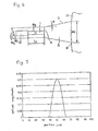
- Fig. 1(a) schematically shows the structure and the operation of the main part of an arrayed waveguide grating type optical multiplexer/demultiplexer according to a first embodiment of the present invention.
- Fig. 1(b) is an enlarged view of an area surrounded by the dotted line (A) in Fig. 1(a).
- Fig. 2 further shows specifics of an end side of one of optical input waveguides 12 in the enlarged view of Fig. 1(b).
- the arrayed waveguide grating type optical multiplexer/demultiplexer is obtained by forming on a substrate 11 an optical waveguide unit 10 that has a waveguide structure.
- the waveguide structure includes at least one optical input waveguide (a first optical waveguide) 12 arranged side by side, a first slab waveguide 13 connected to the exit ends of the optical input waveguides 12, an arrayed waveguide 14 connected to the exit end of the first slab waveguide 13, a second slab waveguide 15 connected to the exit end of the arrayed waveguide 14, and a plurality of optical output waveguides (second optical waveguides) 16 that are arranged side by side and connected to the exit end of the second slab waveguide 15.
- light is input from one of the optical input waveguides 12.
- the arrayed waveguide 14 propagates light that is outputted from the first slab waveguide 13.
- the arrayed waveguide 14 includes a plurality of channel waveguides (14a) that are arranged side by side. Lengths of adjacent channel waveguides (14a) are different from each other by a predetermined length difference ( ⁇ L).
- the optical input waveguides 12 and the optical output waveguides 16 have the same dimension.
- the number of optical output waveguides 16 is determined, for example, in accordance with the number of light beams which have different wavelengths and which are created by demultiplexing signal light with the arrayed waveguide grating type optical multiplexer/demultiplexer.
- the arrayed waveguide 14 usually includes a large number (for example, 100) of the channel waveguides (14a). However, Fig. 1(a) is simplified and the number of the channel waveguides (14a), the optical output waveguides 16, and the optical input waveguides 12 in Fig. 1(a) does not exactly reflect the actual number thereof.
- One of the at least optical input waveguide 12 is connected to, for example, transmission side optical fiber, so that light having undergone the wavelength division multiplexing is introduced to one of the optical input waveguides 12.
- the light which has traveled through one of the optical input waveguides 12 and been introduced to the first slab waveguide 13 is diffracted by the diffraction effect thereof and enters the arrayed waveguide 14 to travel along the arrayed waveguide 14.
- the light Having traveled through the arrayed waveguide 14, the light reaches the second slab waveguide 15 and then is condensed in the optical output waveguides 16 to be outputted therefrom. Because of the preset difference in length between adjacent channel waveguides (14a) of the arrayed waveguide 14, light beams after traveling through the arrayed waveguide 14 have phases different from one another. The wavefront of the light beams is tilted in accordance with this difference and each position where each light beam is condensed is determined by the angle of this tilt. Therefore, the light beams having different wavelengths are condensed at positions different from one another. By forming the optical output waveguides 16 at these positions, the light beams having different wavelengths can be outputted from their respective optical output waveguides 16 that are provided for the respective wavelengths.
- the light having undergone the wavelength division multiplexing and having wavelengths of ⁇ 1, ⁇ 2, ⁇ 3, ..., ⁇ n (n is an integer equal to or larger than 2), is inputted from one of the optical input waveguides 12.
- the light is diffracted in the first slab waveguide 13, reach the arrayed waveguide 14, and travel through the arrayed waveguide 14 and the second slab waveguide 15.
- the light beams are respectively condensed at different positions determined by their wavelengths, enter different optical output waveguides 16, travel along their respective optical output waveguides 16, and are outputted from the exit ends of the respective optical output waveguides 16.
- the light beams having different wavelengths are taken out through optical fibers that are connected to the exit ends of the optical output waveguides 16.
- optical multiplexer/demultiplexer improvement in wavelength resolution is in proportion to the difference in length ( ⁇ L) among the channel waveguides (14a) of the arrayed waveguide 14.
- ⁇ L difference in length
- the optical multiplexer /demultiplexer is designed to have a large ( ⁇ L)
- the optical multiplexer/demultiplexer it is thus possible for the optical multiplexer/demultiplexer to have a function of multiplexing/demultiplexing a plurality of signal light beams, specifically a function of demultiplexing or multiplexing a plurality of optical signals with a wavelength difference of at most 1 nm.
- High density optical wavelength division multiplexing communications require such a small wavelength difference.
- the arrayed waveguide grating type optical multiplexer/demultiplexer is obtained by, for example, forming a waveguide formation region 10 having the above waveguide structure on a substrate 11 made of silicon (Si).
- an under cladding layer SiO2 based glass
- a core layer for example, glass mainly containing SiO2 to which GeO2 is added
- the above waveguide structure is formed by, for example, photolithography and reactive ion etching method.
- the over cladding layer that covers the waveguide structure of the core is formed by flame hydrolysis deposition method.
- the arrayed waveguide grating type optical multiplexer/demultiplexer of this sample is formed such that the height of a core having the above waveguide structure is set to 6.5 ⁇ m, the widths of the optical input waveguide 12 and the optical output waveguides 16 are set to 6.5 ⁇ m, and the relative refractive index difference ( ⁇ ) of the waveguide is set to 0.8 %.
- the optical loss which is the second required performance required for the optical multiplexer/demultiplexer was excellent, that is, 2.0 dB, but the 1dB band width which is the third required characteristic was 0.1 nm and is not satisfied.
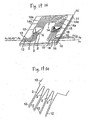
- a tapered waveguide 2 of a tapered structure disclosed in Japanese Unexamined Patent Publication No. Hei 5-313029 is disposed at the output end of the optical input waveguide 12 of the arrayed waveguide grating type optical multiplexer/demultiplexer as shown in Figs. 19(a) and 19(b). Then, an arrayed waveguide grating type optical multiplexer/demultiplexer with 16 channels which can multiplex and demultiplex the lights with the wavelength differences of about 0.8 nm in the 1.55 ⁇ m band was formed, and its characteristics were obtained.
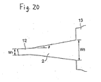
- the tapered waveguide width (W5) at the output end portion (an input end to the first slab waveguide 13) of the tapered waveguide 2 shown in Fig. 20 is set to 25 ⁇ m, and a tapered angle (0) is set to 0.23°.
- the optical loss which is the second required characteristic of the optical multiplexer/demultiplexer is 3.8 dB, and the 1 dB band width of the third required characteristic is 0.3 nm, both of which are excellent.
- the background crosstalk is -28 dB which cannot be satisfied although the adjacent crosstalk is -27 dB which is excellent.
- a slit-shaped waveguide 50 of a slit structure disclosed in Japanese Unexamined Patent Publication No. Hei 8-122557 is disposed at the output end of the optical input waveguide 12 of the arrayed waveguide grating type optical multiplexer/demultiplexer as shown in Figs. 21(a) and 21(b). Then, an arrayed waveguide grating type optical multiplexer/demultiplexer with 16 channels which can multiplex and demultiplex the lights with the wavelength differences of about 0.8 nm in the 1.55 ⁇ m band was formed, and its characteristics were obtained.
- the slit-shaped waveguide 50 has, as shown in Fig. 22, a tapered waveguide portion (2A) whose width gradually increases with a tapered angle (0).
- the tapered waveguide portion (2A) has at its center a trapezoidal slit 19, so that two narrow waveguide portions 8 are spaced apart. The distance between the narrow waveguide portions 8 is gradually increased toward a right direction in Fig. 22 (that is, toward the first slab waveguide 13).
- the upper base of the trapezoidal slit 19 has a width (CW) and the lower base of the trapezoidal slit 19 has a width (SW).
- the waveguide width (W1) of the optical input waveguides 12 is set to 6.5 ⁇ m
- the tapered angle ( ⁇ ) of the tapered waveguide portion (2A) is set to 0.4°
- the width (CW) of the upper base of the trapezoidal slit 19, namely, the width between the narrow width waveguides 8 at the output end of the tapered waveguide portion (2A) is set to 3.2 ⁇ m
- the width (SW) of the lower base of the trapezoidal slit 19, namely, the width between the narrow width waveguides 8 at the input end of the first slab waveguide 13 is set to 5.0 ⁇ m
- a connection portion width (W5) with the fist slab waveguide 13 is set to 18 ⁇ m.
- the heights of the respective waveguides are set to 6.5 ⁇ m
- the relative refractive index difference of the waveguide is set to 0.8 %.
- the 1 dB band width as an index of broadening the band of the third required characteristic to the optical multiplexer/demultiplexer is 0.30 nm which is excellent, but the optical loss which is the second required characteristic is 5 dB which is not satisfied.
- the adjacent crosstalk which is the fourth required characteristic of the optical multiplexer/demultiplexer is -24 dB and the background crosstalk is -27 dB, both of which cannot be satisfied.
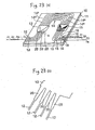
- a parabolic waveguide 20 of a parabolic structure disclosed in Japanese Unexamined Patent Publication No. Hei 9-297228 as shown in Fig. 24 is disposed at the output end of the optical input waveguide 12 of the arrayed waveguide grating type optical multiplexer/demultiplexer as shown in Figs. 23(a) and 23(b).
- an arrayed waveguide grating type optical multiplexer/demultiplexer with 16 channels which can multiplex and demultiplex the lights with the wavelength differences of about 0.8 nm in the 1.55 ⁇ m band was formed, and its characteristics were obtained.
- the width (W1) of the optical input waveguide 12 shown in Fig. 24 is set to 6.5 im
- the parabolic tapered length (L8) is set to 420 ⁇ m
- the parabolic tapered wide end width (W8) is set to 19 ⁇ m.
- the height of the waveguide is set to 6.5 ⁇ m
- the relative refractive index difference of the waveguides are set to 0.8 %.
- the optical loss which is the second required characteristic to the optical multiplexer/demultiplexer is 3.2 dB which is excellent
- the 1 dB band width which is the third required characteristic is 0.22 nm which is excellent
- the background crosstalk which is one of the fourth required characteristics is -33 dB which is excellent, but the adjacent crosstalk is -24 dB which cannot be satisfied.
- 1 dB band width is at least 0.2 nm (preferably at least 0.24 nm)
- the adjacent crosstalk is at most -26 dB
- the background crosstalk is at most -30 dB.
- the arrayed waveguide grating type optical multiplexer/demultiplexer that can satisfy all of the above first to fourth required characteristics of the optical multiplexer/demultiplexer is high in yield cannot be obtained.
- the present inventors simulated the optical amplitude distribution (optical amplitude) of light at the input end of the first slab waveguide 13 utilizing a beam propagation method and obtained the following conception from the above simulating results.
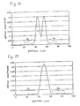
- the optical amplitude distribution is shaped in a mountain having one sharp peak as shown in Fig. 14, and the optical amplitude around the mountain is nearly 0.
- the optical amplitude distribution has one mountain shape with one gentle peak as compared with a case where tapered waveguide 2 is not disposed, as shown in Fig. 15. Also, at both feet ends of the mountain are formed regions (a1 and a2) each having the gentle optical amplitude distribution through a portion the optical amplitude becomes nearly 0 (position (A) in Fig. 15). The regions (a1 and a2) spread the optical amplitude distribution in a direction apart from the center of the mountain peak.
- the optical amplitude distribution has two peaks as shown in Fig. 16, gentle skirt portions (b1 and b2) are formed, and distributions that gently spread at the outer side of those two peaks (in directions apart from the peak centers) are also formed.
- the optical amplitude distribution has one mountain with one gentle peak as compared with a case where parabolic waveguide 20 is not provided, as shown in Fig. 17.
- pleated skirt distributions (c1 and c2) are formed on both ends of the mountain, but the optical amplitude distribution does not spread in directions apart from the center of the peak from the distributions (c1 and c2) portions.
- the present inventors presume the following matters with reference to the respective optical amplitude distributions shown in Figs. 14 to 17, and the study results can be related to the characteristics required for the optical multiplexer/demultiplexer. That is, if the width of portions close to the top of the mountain is wide, the 1 dB band width can be widened; in the case where the spread of the optical amplitude distribution from portions close to the top of the mountain is gentle, the adjacent crosstalk is deteriorated; in the case where the optical amplitude distribution spreads in a direction apart from the center of the peak, the background crosstalk is deteriorated.
- the present inventors consider that the optical amplitude distribution of light that is incident to the first slab waveguide 13 from one of the optical input waveguides 12 is made to have the shape of the following optical amplitude distribution at the entrance of the first slab waveguide 13.
- the present inventors have presumed that if the optical amplitude distribution of light incident to the above first slab waveguide 13 has a mountain shape with only one peak, the width of the top of that mountain is wider than the width of the optical distribution (refer to Fig. 14) of light incident to the first slab waveguide 13 in the arrayed waveguide grating type optical multiplexer/demultiplexer shown in Fig. 18, and the optical amplitude distribution is so shaped as not to provide any one of the regions (a1 and a2) shown in Fig. 15, the skirt portions (b1 and b2) shown in Fig. 16, and the pleated skirt portions (c1 and c2) shown in Fig. 17, the above effects can be exhibited.
- the present inventors have presumed that the above study results can be applied to not only the arrayed waveguide grating type optical multiplexer/demultiplexer, but also various waveguide circuits that constitute other optical multiplexer/demultiplexer or the like.
- the present inventors have conducted a variety of investigations while focusing on the structure of the junction between the optical input waveguides and the first slab waveguide.
- each one of at least one optical input waveguide of the arrayed waveguide grating type optical multiplexer/demultiplexer is connected with the single mode end portion width waveguide having the following characteristic so that the optical amplitude distribution of light incident to the first slab waveguide from the optical input waveguide side (the optical amplitude distribution at the input end portion of the first slab waveguide) has a shape with one peak mountain in which the width of the top of that mountain is wide, and the skirt portions are cut off (that is, a shape having no regions (a1 and a2) shown in Fig. 15, no skirt portions (b1 and b2) shown in Fig. 16, and no pleated skirt portions (c1 and c2) shown in Fig. 17).
- the single mode end portion width waveguide is, for instance, a trapezoidal waveguide 5 whose width increases toward the first slab waveguide side, the oblique lines thereof are almost straight, the upper base (the side facing the optical input waveguide) 4 of the trapezoidal waveguide is wider than the width of the optical input waveguides 12, and the width of the upper base 4 satisfies the single mode condition.
- the optical amplitude distribution of light incident to the first slab waveguide from the optical input waveguide side has a shape with one peak mountain in which portions close to the top are wide as described above by connecting the trapezoidal waveguide structured as described above, and the shkirts portions are cut off.
- the width that satisfies the above single mode condition is obtained as follows.
- the normalized frequency ⁇ of light that is propagated in an optical fiber is generally represented by the following expression 1.
- ⁇ k 0 a n 1 2 - n 0 2
- (a) is the core radius of the optical fiber
- (n 1 ) is refractive index of core
- (n 0 ) is refractive index of cladding
- the relative refractive index difference ( ⁇ ) of the optical waveguide circuit such as the arrayed waveguide grating type optical multiplexer/demultiplexer is 0.8 %
- the wavelength ( ⁇ ) of the propagating light is 1.55 ⁇ m
- the refractive index (n 1 ) is 1.4560
- the refractive index (n 0 ) is 1.4443
- (w) is less than 8.03 ⁇ m.
- the width of the optical input waveguide is 6.5 ⁇ m and the upper base width of the trapezoidal waveguide is less than 8.03 ⁇ m (for example, about 7.5 ⁇ m)
- the above single mode condition is satisfied, and the width can be made wider than the width of the corresponding optical input waveguide, the light incident to the trapezoidal waveguide spreads in the widthwise direction.
- the arrayed waveguide grating type optical multiplexer/demultiplexer includes a trapezoidal waveguide (expanding width waveguide) 5 which has a trapezoidal shape having an upper base (a first end portion) 4 and a lower base (a second end portion) 6.
- the upper base 4 of the trapezoidal waveguide 5 is connected to an optical input waveguide 12 and the lower base 6 is connected to a first slab waveguide 13.
- the width (a second width) (W4) of the lower base 6 is larger than the width (a first width) (W3) of the upper base 4. Further, the first width (W3) satisfies the single mode condition.
- the trapezoidal waveguide 5 that functions as the single mode end portion width waveguide is connected to the output end of the optical input waveguide 12 as the single mode waveguide. Also, the trapezoidal waveguide 5 is a wide width waveguide that widens toward the first slab waveguide 13 side.
- the widths of the respective optical input waveguides 12 are (W1), and the end portion width (upper base 4) of the trapezoidal waveguide 5 opposite to the arrayed waveguide 14 is (W3).
- the trapezoidal waveguide 5 widens at a tapered angle ⁇ , and the oblique line 3 of the trapezoidal waveguide 5 is substantially straight.
- the upper base 4 of the trapezoidal waveguide 5 has a width (W3) which is larger than the width of the corresponding optical input waveguide 12.
- the lower base 6 is slightly curved and has the width (W4).
- the above parameters are set as follows: the width (W1) of each of the optical input waveguides 12 is equal to 6.5 ⁇ m, the width (W3) of the trapezoidal waveguide 5 at the upper base 4 is equal to 7.5 ⁇ m, the taper angle ( ⁇ ) is equal to 0.2E, and the width (W4) of the trapezoidal waveguide 5 at the lower base 6 is equal to 19.0 ⁇ m.
- the arrayed waveguide grating type optical multiplexer/demultiplexer according to the first embodiment may multiplex and demultiplex optical signals in the 1.55 ⁇ m band whose wavelengths are different from each other by at least about 0.8 nm (in other words, with a frequency difference of at least about 100 GHz).
- one of the at least one optical input waveguide 12 is connected to, for example, transmission side optical fiber so that light that has undergone wavelength division multiplexing is introduced to one of the optical input waveguides 12.
- the light that has traveled through one of the optical input waveguides 12 enters the trapezoidal waveguide 5.
- the light entered to the trapezoidal waveguide 5 is broadened along the width of the waveguide.
- the light then travels along the trapezoidal waveguide 5 while changing its optical amplitude distribution.
- the width of the trapezoidal waveguide 5 increases toward the first slab waveguide 13, the width of the top portion in the optical amplitude distribution is widened, and the base portions of the optical amplitude distribution are cut off as the light travels.
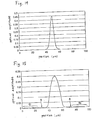
- Fig. 3 shows the optical amplitude distribution at the input end of the first slab waveguide 13 when the optical amplitude distribution is simulated through a beam propagation method.
- the optical amplitude distribution has one top portion, and the width around the top portion is wide, and the rising of the skirt portions (both end sides of the optical amplitude distribution curve) is excellent, namely, the curve has no (a1 and a2) regions shown in Fig. 15, no skirt portions (b1 and b2) shown in Fig. 16 and no pleated skirt portions (c1 and c2) shown in Fig. 17.
- each optical input waveguide 12 is connected to the first slab waveguide 13 via each trapezoidal waveguide 5. Accordingly, the optical amplitude distribution changes as described above.
- the optical amplitude distribution of light at the output end of the trapezoidal waveguide 5 (in other words, at the entrance of the first slab waveguide 13) thus has the shape as shown in Fig. 3.
- each trapezoidal waveguide 5 has the width which increases toward the first slab waveguide 13 and has the oblique lines 3 that are substantially straight. Further, each optical input waveguide 12 is connected to the first slab waveguide 13 via each trapezoidal waveguide 5. Accordingly, an arrayed waveguide grating type optical multiplexer/demultiplexer with a simple structure may be obtained. Further, an arrayed waveguide grating type optical multiplexer/demultiplexer with a high yield may be readily manufactured.
- a plurality of arrayed waveguide grating type optical multiplexers/demultiplexers according to the present embodiment were manufactured on the basis of the above design values, and the performances of those multiplexers/demultiplexers were studied.
- Fig. 4 shows a spectrum representative of the wavelength characteristic of the optical transmittance of the sample according to the present embodiment.
- FIG. 5(a) schematically shows a perspective view of the main structure of the arrayed waveguide grating type optical multiplexer/demultiplexer in accordance with the second embodiment of the present invention together with its operation
- Fig. 5(b) shows an enlarged plan view of a portion surrounded by a dotted line (A) shown in Fig. 5(a).
- Fig. 6 shows the specific example of the end portion of one optical input waveguide 12 in the enlarged diagram.
- a straight waveguide (narrow width straight waveguide) 1 is interposed between the optical input waveguide 12 and the trapezoidal waveguide 5.
- the width of the straight waveguide is narrower than that of the corresponding optical input waveguide 12.
- the centers of the respective straight waveguides 1 in the widthwise direction are positioned at the center of the input ends of the corresponding trapezoidal waveguides 5 in the widthwise direction.
- the respective straight waveguides 1 form an optical power center position adjusting means that moves the power center of the light that has been propagated through the optical input waveguide 12 to the center of the straight waveguide 1 in the widthwise direction and makes the light power center incident to the center of the input end of the trapezoidal waveguide 5 in the widthwise direction.
- the width of the straight waveguide 1 is (W2) and its length is (L1).
- the width (W2) of the straight waveguide 1 is set to 3.0 ⁇ m
- the length (L1) of the straight waveguide 1 is set to 500 ⁇ m
- other parameters (W1, W3, ⁇ , W4) are the same values as the parameters in the above-described first embodiment.
- the arrayed waveguide grating type optical multiplexer/demultiplexer according to the second embodiment may multiplex and demultiplex optical signals in the 1.55 ⁇ m band whose wavelengths are different from each other by at least about 0.8 nm.
- the second embodiment is structured as described above, and in the second embodiment, the wavelength multiplexed light introduced into the optical input waveguide 12 is made incident to the straight waveguide 1, and the center of the optical power is moved to the center of the straight waveguide 1 by the straight waveguide 1, and the center of the optical power is made incident to the center of the trapezoidal waveguide 5 in the widthwise direction.
- the light incident to the trapezoidal waveguide 5 spreads in the waveguide widthwise direction as in the above first embodiment, and then advances while the optical amplitude distribution is changed in the trapezoidal waveguide 5. Then, it is presumed that the width of the optical amplitude distribution close to the mountain top portion expands and the skirt portions of the optical amplitude distribution are cut off as the light advances as described in the above first embodiment.
- Fig. 7 shows an optical amplitude distribution at the input end of the first slab waveguide 13 when the optical amplitude distribution is simulated through a beam propagation method.
- the optical amplitude distribution has one top portion in which the width close to the top portion is wide and the rising of the skirt portion (both end sides) is excellent, as explained in the above first embodiment.
- the second embodiment may have the same effects as those in the above first embodiment.
- the straight waveguide 1 is interposed between the optical input waveguide 12 and the trapezoidal waveguide 5
- the center of the light intensity can be made incident to the center of the trapezoidal waveguide 5 in the widthwise direction by the straight waveguide 1.
- the center position of the light intensity that is propagated through the optical input waveguide 12 is displaced from the center position of the optical input waveguide 12 in the widthwise direction, the center position of the optical intensity is made incident to the center of the trapezoidal waveguide 5 in the widthwise direction, and the optical amplitude distribution can be more surely made into the above shape, thereby being capable of providing the arrayed waveguide grating type optical multiplexer/demultiplexer which is excellent in the loss characteristic, the 1dB band width, the adjacent crosstalk and the background crosstalk.
- samples according to the second embodiment of the present invention will be described.
- a plurality of samples of the arrayed waveguide grating type optical multiplexers/demultiplexers according to the second embodiment were manufactured on the basis of the above design values, and the performances of those multiplexers/demultiplexers were studied.
- the loss was 2.7 dB
- the 1dB band width was 0.26 nm
- the adjacent crosstalk was -31 dB
- the background crosstalk was -37 dB. All characteristics were excellent.
- the 1dB band width, the adjacent crosstalk and the background crosstalk in the samples of the arrayed waveguide grating type optical multiplexer/demultiplexer having the same design of the above second embodiment it was recognized that the variations among the samples were small.
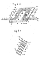
- FIG. 8(a) schematically shows a perspective view of the main structure of the arrayed waveguide grating type optical multiplexer/demultiplexer in accordance with the third embodiment together with its operation
- Fig. 8(b) shows an enlarged plan view of a portion surrounded by a dotted line (A) shown in Fig. 8(a).
- Fig. 9 shows the specific example of the end portion of one optical input waveguide 12 in the enlarged diagram.
- the optical input waveguide 12 is connected to the trapezoidal waveguide 5 via an equal width waveguide 9 .
- the constant-width waveguide 9 has a width which is same as that of the narrow width end of the trapezoidal waveguide 5.
- the trapezoidal waveguide 5 that functions as the wide width waveguide that widens toward the arrayed waveguide side is disposed at the output end of the constant-width waveguide 9 that functions as the single mode waveguide.
- the width (W3) of the constant-width waveguide 9 (the width of the upper base 4 of the trapezoidal waveguide 5) is set to 7.5 ⁇ m
- the length (L2) of the constant-width waveguide 9 is set to 250 ⁇ m
- other parameters (W1, ⁇ , W4) are the same values as the parameters in the above-described first embodiment.
- the arrayed waveguide grating type optical multiplexer/demultiplexer according to the third embodiment may multiplex and demultiplex optical signals in the 1.55 ⁇ m band whose wavelengths are different from each other by at least about 0.8 nm.
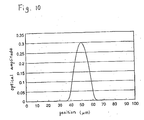
- Fig. 10 shows an optical amplitude distribution at the incident end of the first slab waveguide 13 when the optical amplitude distribution is simulated through a beam propagation method.
- the optical amplitude distribution shown in the figure has one top portion. The width close to the top portion is wide and the rising of the skirt portion (both end sides) is excellent, as explained in the above first embodiment.
- samples according to the third embodiment of the present invention will be described.
- a plurality of samples of the arrayed waveguide grating optical multiplexer/demultiplexer according to the third embodiment were manufactured on the basis of the above design values, and the performances of the multiplexers/demultiplexers were studied.
- the loss was 2.8 dB
- the 1dB band width was 0.26 nm
- the adjacent crosstalk was -31 dB
- the background crosstalk was -32 dB.
- the 1dB band width, the adjacent crosstalk and the background crosstalk in the samples of the arrayed waveguide grating type optical ltiplexer/demultiplexer having the same design of the third embodiment it was recognized that the variations among the samples were small.
- FIG. 11(a) schematically shows a perspective view of the main structure of the arrayed waveguide grating type optical multiplexer/demultiplexer in accordance with the fourth embodiment together with its operation
- Fig. 11(b) shows an enlarged plan view of a portion surrounded by a dotted line (A) shown in Fig. 11(a).
- Fig. 12 shows the specific example of the end portion of one optical input waveguide 12 in the enlarged diagram.
- the optical input waveguide 12 is connected to the trapezoidal waveguide 5 via a straight waveguide (narrow width straight waveguide) 1 and a constant-width waveguide 9.
- the width of the straight waveguide 1 is narrower than the width of the optical input waveguide 12.
- the centers of the respective straight waveguides 1 in the widthwise direction are positioned at the center of the incident ends of the corresponding constant-width waveguides 9 in the widthwise direction.
- the respective straight waveguides 1 move the power center of the light that has been propagated through the optical input waveguide 12 to the center of the straight waveguide 1 in the widthwise direction and makes the light power center incident to the center of the incident end of the constant-width waveguide 9 in the widthwise direction.
- the width of the straight waveguide 1 is (W2) and its length is (L1).
- the width (W2) of the straight waveguide 1 is set to 3.0 ⁇ m
- the length (L1) of the straight waveguide 1 is set to 500 ⁇ m
- other parameters (W1, W3, ⁇ , W4, L2) are set to the same values as the parameters in the above-described third embodiment.
- the arrayed waveguide grating type optical multiplexer/demultiplexer according to the fourth embodiment may multiplex and demultiplex optical signals in the 1.55 ⁇ m band whose wavelengths are different from each other by at least about 0.8 nm.
- the fourth embodiment is structured as described above, and in the fourth embodiment, the wavelength multiplex light introduced into the optical input waveguide 12 is made incident to the straight waveguide 1, and the center of the optical power is moved to the center of the straight waveguide 1 by the straight waveguide 1, and the center of the light power is made incident to the center of the constant-width waveguide 9 in the widthwise direction.
- the light incident to the constant-width waveguide 9 spreads in the waveguide widthwise direction as explained in the above second embodiment, and is then advanced while the optical amplitude distribution is changed in the trapezoidal waveguide 5 with the same effects as those in the above third embodiment.
- Fig. 13 shows an optical amplitude distribution at the incident end of the first slab waveguide 13 when the optical amplitude distribution is simulated through a beam propagation method.
- the optical amplitude distribution shown in Fig. 13 has one top portion in which the width close to the top portion is wide and the rising of the skirts portion (both end sides) is excellent, as explained in the above respective embodiments.
- the straight waveguide 1 is interposed between the optical input waveguide 12 and the constant-width waveguide 9, the center of the light intensity can be made incident to the center of the constant-width waveguide 9 in the widthwise direction by the straight waveguide 1.
- the center position of the light intensity that is propagated through the optical input waveguide 12 is displaced from the center position of the optical input waveguide 12 in the widthwise direction, the center position of the light intensity is made incident to the center of the constant-width waveguide 9 in the widthwise direction, and the optical amplitude distribution can be more surely made into the shape as shown in Fig. 13. Accordingly, the arrayed waveguide grating type optical multiplexer/demultiplexer which is excellent in the loss characteristic, the 1dB band width, the adjacent crosstalk and the background crosstalk may be obtained.
- samples according to the fourth embodiment of the present invention will be described.
- a plurality of samples of the arrayed waveguide grating type optical multiplexers/demultiplexers according to the fourth embodiment were manufactured on the basis of the above design values, and the performances of those multiplexers/demultiplexers were studied.
- the loss was 2.8 dB
- the 1dB band width was 0.26 nm
- the adjacent crosstalk was -30 dB
- the background crosstalk was -35 dB.
- the 1dB band width, the adjacent crosstalk and the background crosstalk in the arrayed waveguide grating type optical multiplexer/demultiplexer having the same design of the above fourth embodiment it was recognized that all the variations among the samples were small.
- each of all optical output waveguides 16 may be connected to the second slab waveguide 15 via each trapezoidal waveguide 5.
- each trapezoidal waveguide 5 may be connected to each of all optical output waveguides 16 via each straight wavegude 1.
- each trapezoidal waveguide 5 may be connected to each of all optical output waveguides 16 via each equal width waveguide 9.
- each trapezoidal waveguide 5 may be connected to each of all optical output waveguides 16 via each straight waveguide 1 and each equal width waveguide 9. Further, referring to Fig.
- each optical input waveguide 12 may be connected to the first slab waveguide 13 via each trapezoidal waveguide 5, and each of all optical output waveguides 16 may also be connected to the second slab waveguide 15 via each trapezoidal waveguide 5.
- each trapezoidal waveguide 5 may be connected to each optical input waveguide 12 via each straight wavegude and/or each equal width waveguide.
- each trapezoidal waveguide 5 may be connected to each optical output waveguide 16 via each straight wavegude and/or each equal width waveguide.
- some of all optical input waveguides 12 may be connected to the first slab waveguide 13 via each trapezoidal waveguide 5, and other optical input waveguides 12 may be directly connected to the first slab waveguide 13 without interposing the trapezoidal waveguide 5.
- the width of the trapezoidal waveguide 5 increases toward the arrayed waveguide 14 side, and the end portion width of the trapezoidal waveguide 5 opposite to the arrayed waveguide 14 is wider than the width of the corresponding optical input waveguide 12 or optical output waveguide 16 and satisfies the single mode condition. Therefore, above described effects may be obtained.
- each trapezoidal waveguide 5 is provided at each output end of a plurality of optical output waveguides 16, the straight waveguide 1 as the one described in the second embodiment may be interposed between each optical output waveguide 16 and each trapezoidal waveguide 5. It is also possible to form the constant width waveguide 9 and/or the straight waveguide (narrow straight waveguide) 1 between each optical output waveguide 16 and each trapezoidal waveguide 5 as explained in the third and fourth embodiments.
- the width of the upper base 4 of the trapezoidal waveguide 5 has to be wider than the optical output waveguides 16 and width of the upper base 4 satisfies the single mode condition if each trapezoidal waveguide 5 is provided at each output end of the optical output waveguides 16.
- the straight waveguide 1 has to be narrower than the optical output waveguides 16 if each straight waveguide 1 is interposed between each optical output waveguide 16 and each trapezoidal waveguide 5.
- the oblique lines of the trapezoidal waveguide 5 can be substantially straight.
- the embodiments according to the present invention does not put particular limitation in the width, the length and the taper angle of the trapezoidal waveguide, the width and the length of the straight waveguide, and the length of the constant width waveguide, and these parameters are suitably set. If these parameters are set in accordance with specifications of an arrayed waveguide grating type optical multiplexer/demultiplexer and based on the results of simulation of the optical amplitude distribution as shown in Figs. 3, 7, 10, and 13, for example, the arrayed waveguide grating type optical multiplexer/demultiplexer can have the excellent effects described in the above embodiments.
- the expanding width waveguide to be applied to the arrayed waveguide grating type optical multiplexer/ demultiplexer according to the embodiments of the present invention does not necessarily include trapezoidal waveguide. It is sufficient for the single mode end portion width waveguide to be wider than a width of a corresponding optical input waveguide and an optical output waveguide, and to have a wide enough end portion width satisfying the single mode condition and to have a wide width waveguide increasing toward the arrayed waveguide in at least a part thereof a waveguide.
- the structure of the expanding width waveguide according to the embodiments of the present invention as shown in, for example, Figs. 2, 6, 9 and 12 are adopted as a part of the circuit structure of the arrayed waveguide grating type optical multiplexer/demultiplexer in the above embodiments.
- the expanding width waveguide according to the embodiments of the present invention can be applied to an optical waveguide circuit of a circuit structure other than the arrayed waveguide grating type optical multiplexer/demultiplexer.
- the expanding width waveguide according to the embodiments of the present invention is not always limited to the structure having the trapezoidal waveguide, but may be structured in such a manner that the single mode end portion width waveguide has an end portion width that is wider than the width of the corresponding optical input waveguide or optical output waveguide and satisfies the single mode condition, and the wide width waveguide that widens toward the arrayed waveguide side is disposed on at least a part of the single mode end portion width waveguide.
- the single mode end portion width waveguide having an end portion width which is wider than the width of the corresponding optical input waveguide and satisfies the single mode condition is connected to, for example, an output end of the optical input waveguide, and the wide width waveguide that widens toward the arrayed waveguide side is disposed on at least a part of the single mode end portion width waveguide.
- the end portion (an end portion of the optical input waveguide side) of the single mode end portion width waveguide opposite to the arrayed waveguide has a width which is wider than the width of the corresponding optical input waveguide and satisfies the single mode condition.
- the loss is low, the 1 dB band width is wide, and the adjacent crosstalk and background crosstalk are low.
- the above single mode end portion width waveguide can be formed of, for example, a trapezoidal waveguide that widens toward the arrayed waveguide side.
- the single mode end portion width waveguide can be so structured as to have a trapezoidal waveguide as the wide width waveguide.
- the light is widened in the widthwise direction of the trapezoidal waveguide, and thereafter the optical amplitude distribution can be shaped into one mountain in which the width close to the top is wide and the rising of the skirt portions is excellent, thereby being capable of providing the above effects.
- the structure according to the embodiments of the present invention is simple, and hence can provide an arrayed waveguide grating type optical multiplexer/demultiplexer with a high yield which is easy to manufacture.
- the arrayed waveguide grating type optical multiplexer/demultiplexer has the reciprocity of an optical circuit
- the arrayed waveguide grating type optical multiplexer/demultiplexer according to the embodiments of the present invention even in the case where each single mode end portion width waveguide having an end portion width which is wider than the width of the corresponding optical output waveguide and satisfies the single mode condition is connected to each entrance end of the optical output waveguide, and the wide width waveguide that widens toward the arrayed waveguide side is disposed on at least a part of the single mode end portion width waveguide, the same effects can be obtained.
- the above single mode end portion width waveguide can be formed of, for example, a trapezoidal waveguide that widens toward the arrayed waveguide side.
- the single mode end portion width waveguide can be so structured as to have a trapezoidal waveguide as the wide width waveguide.
- the arrayed waveguide grating type optical multiplexer/demultiplexer is capable of making the overall intensity distribution shape of light that outputs from the wide width waveguide such as the trapezoidal waveguide free from deformation. This is achieved by providing a straight waveguide narrower than the optical input waveguides between each optical input waveguide and such as each trapezoidal waveguide. Alternatively, this is achieved by providing, in the structure where the constant width waveguide is formed, a narrow straight waveguide between the constant waveguide and its associated optical input waveguide.
- the central position of the light intensity distribution can be moved to the center of the straight waveguide when the light travels along the straight waveguide.
- the light intensity center thus can be inputted in the center in the width direction of the wide width waveguide of such as the trapezoidal waveguide.
- the arrayed waveguide grating type optical multiplexer/demultiplexer utilizes the reciprocity of the optical circuit. It is therefore possible to obtain the same effect as above also with the arrayed waveguide grating type optical multiplexer/demultiplexer according to the embodiments of the present invention in which the straight waveguide narrower than the optical output waveguide is interposed between each wide width waveguide such as the trapezoidal waveguide and each of the optical output waveguides. Furthermore, the arrayed waveguide grating type optical multiplexer/demultiplexer according to the embodiments of the present invention in which the narrow straight waveguide is interposed between each constant width waveguide and each of the optical output waveguides can also provide the same effect.
- the single mode end portion width waveguide having an end portion width which is wider than the width of the single mode waveguide and satisfies the single mode condition is connected to the single mode waveguide, and the wide width waveguide that widens toward arrayed waveguide side is disposed on at least a part of the single mode end portion width waveguide.
- the above structure is applied to various circuit structures such as the arrayed waveguide grating type optical multiplexer/demultiplexer, it is capable of improving the flatness of, for example, a light that is multiplexed and demultiplexed and of exhibiting such effects that the adjacent crosstalk and the background crosstalk can be lessened.
- the single mode end portion width waveguide is such as the trapezoidal waveguide
- the above effects can be efficiently exerted with a very simple structure.
- the embodiments of the present invention place the single mode end poriton width waveguide whose width increases toward the arrayed waveguide, such as the trapezoidal waveguide described above, on the output end of each of the optical input waveguides, for example.
- This makes it possible to form the optical amplitude distribution of light that is outputted from the single mode end portion width waveguide to enter the first slab waveguide into a mountain shape in which the width close to the top of the mountain is wide and the skirt portions are cut off.
- the embodiments of the present invention thus can provide an arrayed waveguide grating type optical multiplexer/demultiplexer in which the 1 dB band width is wide, the loss is low, and the adjacent crosstalk and background crosstalk are low.
- the single mode end portion width waveguide can be made into, for example, a trapezoidal waveguide per se as described above or can be so structured as to have a trapezoidal waveguide as the wide width waveguide.
- the embodiments of the present invention is capable of making the overall intensity distribution shape of light that is outputted from the trapezoidal waveguide free from deformation. This is achieved by providing a straight waveguide narrower than the optical input waveguide between, for example, the optical input waveguide and the trapezoidal waveguide. Because of this straight waveguide, even if the optical input waveguide has a curved portion and the central position of the light intensity distribution is deviated from the center in width of the optical input waveguide after the light has traveled through this carved portion, the central position of the light intensity distribution can be moved to the center of the straight waveguide during the light travels along the straight waveguide. The light intensity center thus can be inputted in the center in width of the trapezoidal waveguide.
- the arrayed waveguide grating type optical multiplexer/demultiplexer is formed by utilizing the reciprocity of an optical circuit, similarly in the case where each of input ends of the respective optical output waveguides is connected with each single mode end portion width waveguide having an end portion width that is wider than the width of the corresponding optical output waveguide and satisfies the single mode condition, and the wide width waveguide which is widened toward the arrayed waveguide side is disposed on at least a part (in its longitudinal direction) of the single mode end portion width waveguide, there can be provided the arrayed waveguide grating type optical multiplexer/demultiplexer in which the 1dB band width is wide, the loss is low, and the adjacent crosstalk and the background crosstalk are low.
- the single mode end portion width waveguide has the width at a optical output waveguide side which is wider than the width of the corresponding optical output waveguide and satisfies the single mode condition.
- the structure of the arrayed waveguide grating type optical multiplexer/demultiplexer according to the embodiments of the present invention is simple, manufacturing thereof is easy and it makes an arrayed waveguide grating type optical multiplexer/demultiplexer with high production yield.
- the arrayed waveguide grating is utilized as a demultiplexer, the arrayed waveguide grating may also be utilized as a multiplexer. In such a case, light is input from the second optical waveguides 16 and output from one of the first optical waveguide 12.
Applications Claiming Priority (2)
| Application Number | Priority Date | Filing Date | Title |
|---|---|---|---|
| JP2000400362A JP2002202419A (ja) | 2000-12-28 | 2000-12-28 | アレイ導波路回折格子型光合分波器および光導波回路 |
| JP2000400362 | 2000-12-28 |
Publications (2)
| Publication Number | Publication Date |
|---|---|
| EP1219989A2 true EP1219989A2 (de) | 2002-07-03 |
| EP1219989A3 EP1219989A3 (de) | 2004-04-07 |
Family
ID=18864969
Family Applications (1)
| Application Number | Title | Priority Date | Filing Date |
|---|---|---|---|
| EP01310916A Withdrawn EP1219989A3 (de) | 2000-12-28 | 2001-12-28 | Ein optischer Multiplexer/Demultiplexer vom Wellenleitergittertyp |
Country Status (5)
| Country | Link |
|---|---|
| US (1) | US6501882B2 (de) |
| EP (1) | EP1219989A3 (de) |
| JP (1) | JP2002202419A (de) |
| KR (1) | KR20020055445A (de) |
| CN (1) | CN1362805A (de) |
Families Citing this family (17)
| Publication number | Priority date | Publication date | Assignee | Title |
|---|---|---|---|---|
| JP4460031B2 (ja) * | 2000-03-28 | 2010-05-12 | 古河電気工業株式会社 | アレイ導波路型回折格子 |
| JP3566940B2 (ja) * | 2000-04-18 | 2004-09-15 | 古河電気工業株式会社 | アレイ導波路回折格子型光合分波器 |
| US6920265B2 (en) * | 2000-12-28 | 2005-07-19 | The Furukawa Electric Co., Ltd. | Arrayed waveguide grating type optical multiplexer/demultiplexer |
| JP3994860B2 (ja) * | 2002-11-19 | 2007-10-24 | 富士通株式会社 | アレイ導波路型回折格子 |
| JP2007065562A (ja) * | 2005-09-02 | 2007-03-15 | Furukawa Electric Co Ltd:The | アレイ導波路回折格子 |
| CN100403078C (zh) * | 2006-06-23 | 2008-07-16 | 华为技术有限公司 | 一种光分插复用装置、系统及其升级扩展方法 |
| JP4748524B2 (ja) * | 2006-08-31 | 2011-08-17 | 古河電気工業株式会社 | アレイ導波路格子型合分波器 |
| JP5100175B2 (ja) * | 2007-03-28 | 2012-12-19 | 古河電気工業株式会社 | アレイ導波路格子型の合分波装置 |
| JP2010276639A (ja) * | 2009-05-26 | 2010-12-09 | Furukawa Electric Co Ltd:The | アレイ導波路格子 |
| US20110085761A1 (en) * | 2009-05-26 | 2011-04-14 | Furukawa Electric Co., Ltd. | Arrayed waveguide grating and method of manufacturing arrayed waveguide grating |
| US20150049998A1 (en) * | 2013-08-13 | 2015-02-19 | Futurewei Technologies, Inc. | Compact Optical Waveguide Arrays and Optical Waveguide Spirals |
| US20160334648A1 (en) * | 2015-05-15 | 2016-11-17 | Huawei Technologies Canada Co., Ltd. | Optical Phase Shifter |
| CN105137538A (zh) * | 2015-10-15 | 2015-12-09 | 中国科学院半导体研究所 | 一种阵列波导光栅光谱平坦化的方法 |
| JP6711025B2 (ja) * | 2016-03-03 | 2020-06-17 | 株式会社豊田中央研究所 | グレーティングカプラ、グレーティングカプラアレイ、結像光学系、光スキャナ、及びレーザレーダ装置 |
| US10678004B2 (en) * | 2018-08-01 | 2020-06-09 | Lumentum Operations Llc | Multiple waveguide alignment |
| CN111679365B (zh) * | 2020-05-29 | 2021-08-06 | 北京邮电大学 | 一种四通道硅基阵列波导光栅波分复用器 |
| CN112305668B (zh) * | 2020-10-21 | 2022-04-19 | 浙江大学 | 一种双层结构的阵列波导光栅 |
Citations (7)
| Publication number | Priority date | Publication date | Assignee | Title |
|---|---|---|---|---|
| EP0484878A2 (de) * | 1990-11-05 | 1992-05-13 | Nippon Sheet Glass Co., Ltd. | Optische Schaltung mit Y-Verzweigung |
| JPH05313029A (ja) * | 1992-05-13 | 1993-11-26 | Nippon Telegr & Teleph Corp <Ntt> | 光合分波器 |
| US5537432A (en) * | 1993-01-07 | 1996-07-16 | Sdl, Inc. | Wavelength-stabilized, high power semiconductor laser |
| FR2742882A1 (fr) * | 1995-12-22 | 1997-06-27 | Corning Inc | Demultiplexeur de longueurs d'onde, realise en optique integree |
| US5748811A (en) * | 1995-09-14 | 1998-05-05 | Bell Communications Research, Inc. | Optical switch |
| US6069990A (en) * | 1997-11-27 | 2000-05-30 | Hitachi Cable Ltd. | Optical wavelength multiplexer/demultiplexer |
| US6195482B1 (en) * | 1998-12-29 | 2001-02-27 | Lucent Technologies Inc. | Waveguide grating router |
Family Cites Families (6)
| Publication number | Priority date | Publication date | Assignee | Title |
|---|---|---|---|---|
| US5467415A (en) * | 1994-04-22 | 1995-11-14 | At&T Corp. | Method for making polarization independent silica optical circuits |
| JPH1084333A (ja) * | 1996-09-10 | 1998-03-31 | Fujitsu Ltd | 波長多重光送信器及び波長多重分離光送受信システム |
| US6281997B1 (en) * | 1997-09-11 | 2001-08-28 | Ciena Corporation | Dense WDM optical multiplexer and demultiplexer |
| US6351581B1 (en) * | 1998-03-17 | 2002-02-26 | Agere Systems Optoelectronics Guardian Corp. | Optical add-drop multiplexer having an interferometer structure |
| US6212315B1 (en) * | 1998-07-07 | 2001-04-03 | Lucent Technologies Inc. | Channel power equalizer for a wavelength division multiplexed system |
| US6421478B1 (en) * | 1999-05-11 | 2002-07-16 | Jds Fitel Inc. | Tapered MMI coupler |
-
2000
- 2000-12-28 JP JP2000400362A patent/JP2002202419A/ja active Pending
-
2001
- 2001-12-27 US US10/026,722 patent/US6501882B2/en not_active Expired - Fee Related
- 2001-12-28 EP EP01310916A patent/EP1219989A3/de not_active Withdrawn
- 2001-12-28 CN CN01138639A patent/CN1362805A/zh active Pending
- 2001-12-28 KR KR1020010087097A patent/KR20020055445A/ko active IP Right Grant
Patent Citations (7)
| Publication number | Priority date | Publication date | Assignee | Title |
|---|---|---|---|---|
| EP0484878A2 (de) * | 1990-11-05 | 1992-05-13 | Nippon Sheet Glass Co., Ltd. | Optische Schaltung mit Y-Verzweigung |
| JPH05313029A (ja) * | 1992-05-13 | 1993-11-26 | Nippon Telegr & Teleph Corp <Ntt> | 光合分波器 |
| US5537432A (en) * | 1993-01-07 | 1996-07-16 | Sdl, Inc. | Wavelength-stabilized, high power semiconductor laser |
| US5748811A (en) * | 1995-09-14 | 1998-05-05 | Bell Communications Research, Inc. | Optical switch |
| FR2742882A1 (fr) * | 1995-12-22 | 1997-06-27 | Corning Inc | Demultiplexeur de longueurs d'onde, realise en optique integree |
| US6069990A (en) * | 1997-11-27 | 2000-05-30 | Hitachi Cable Ltd. | Optical wavelength multiplexer/demultiplexer |
| US6195482B1 (en) * | 1998-12-29 | 2001-02-27 | Lucent Technologies Inc. | Waveguide grating router |
Non-Patent Citations (2)
| Title |
|---|
| LORENZO R M ET AL: "IMPROVED SELF-IMAGING CHARACTERISTICS IN 1 X N MULTIMODE COUPLERS" IEE PROCEEDINGS: OPTOELECTRONICS, INSTITUTION OF ELECTRICAL ENGINEERS, STEVENAGE, GB, vol. 145, no. 1, 1 February 1998 (1998-02-01), pages 65-69, XP000780219 ISSN: 1350-2433 * |
| PATENT ABSTRACTS OF JAPAN vol. 018, no. 126 (P-1702), 2 March 1994 (1994-03-02) & JP 05 313029 A (NIPPON TELEGR & TELEPH CORP), 26 November 1993 (1993-11-26) * |
Also Published As
| Publication number | Publication date |
|---|---|
| US20020122627A1 (en) | 2002-09-05 |
| US6501882B2 (en) | 2002-12-31 |
| EP1219989A3 (de) | 2004-04-07 |
| KR20020055445A (ko) | 2002-07-08 |
| JP2002202419A (ja) | 2002-07-19 |
| CN1362805A (zh) | 2002-08-07 |
Similar Documents
| Publication | Publication Date | Title |
|---|---|---|
| CA2198836C (en) | Optical wavelength multiplexer/demultiplexer | |
| JP2693354B2 (ja) | 光デバイス | |
| EP1219989A2 (de) | Ein optischer Multiplexer/Demultiplexer vom Wellenleitergittertyp | |
| CA2212975C (en) | Optical wavelength multiplexer/demultiplexer | |
| US5940555A (en) | Optical multiplexer/demultiplexer | |
| US20020015559A1 (en) | Arrayed waveguide grating type optical multiplexer/demultiplexer and optical waveguide circuit | |
| EP1045263A1 (de) | Optischer multiplexer/demultiplexer mit wellenleiterarray-beugungsgitter | |
| US6404946B1 (en) | Arrayed waveguide grating type optical multiplexer/demultiplexer | |
| EP1113297A2 (de) | Wellenleitergitter-Multiplexer mit sich verjüngenden Wellenleitern | |
| EP1251652A2 (de) | Wellenleiter-Gitter optischer Multiplexer/Demultiplexer | |
| US6741772B2 (en) | Optical multiplexer/demultiplexer and waveguide type optical coupler | |
| JPH05313029A (ja) | 光合分波器 | |
| US6798952B2 (en) | Optical multiplexer/demultiplexer | |
| JPH11160556A (ja) | 光波長合分波器 | |
| US6728435B2 (en) | Arrayed waveguide grating type optical multiplexer/demultiplexer and optical waveguide circuit | |
| KR100594040B1 (ko) | 듀얼 밴드 파장분할 다중화기 | |
| US6920265B2 (en) | Arrayed waveguide grating type optical multiplexer/demultiplexer | |
| CA2443416C (en) | Optical multi-demultiplexer | |
| US7065273B2 (en) | Wideband arrayed waveguide grating | |
| JPH11218624A (ja) | 光波長合分波器 | |
| US6574397B2 (en) | Optical multiplexer/demultiplexer | |
| EP4202510A1 (de) | Integrierte optische struktur zum multiplexen und/oder demultiplexen | |
| JPH09171112A (ja) | アレイ導波路格子 | |
| WO2003065098A1 (en) | Integrated photonic device and method of making the photonic device |
Legal Events
| Date | Code | Title | Description |
|---|---|---|---|
| PUAI | Public reference made under article 153(3) epc to a published international application that has entered the european phase |
Free format text: ORIGINAL CODE: 0009012 |
|
| 17P | Request for examination filed |
Effective date: 20020117 |
|
| AK | Designated contracting states |
Kind code of ref document: A2 Designated state(s): AT BE CH CY DE DK ES FI FR GB GR IE IT LI LU MC NL PT SE TR |
|
| AX | Request for extension of the european patent |
Free format text: AL;LT;LV;MK;RO;SI |
|
| PUAL | Search report despatched |
Free format text: ORIGINAL CODE: 0009013 |
|
| AK | Designated contracting states |
Kind code of ref document: A3 Designated state(s): AT BE CH CY DE DK ES FI FR GB GR IE IT LI LU MC NL PT SE TR |
|
| AX | Request for extension of the european patent |
Extension state: AL LT LV MK RO SI |
|
| RIC1 | Information provided on ipc code assigned before grant |
Ipc: 7G 02B 6/12 B Ipc: 7G 02B 6/34 B Ipc: 7G 02B 6/293 A |
|
| 17Q | First examination report despatched |
Effective date: 20040709 |
|
| AKX | Designation fees paid |
Designated state(s): DE FR GB |
|
| STAA | Information on the status of an ep patent application or granted ep patent |
Free format text: STATUS: THE APPLICATION IS DEEMED TO BE WITHDRAWN |
|
| 18D | Application deemed to be withdrawn |
Effective date: 20050110 |