EP1217498A2 - Taktgeber zur Erzeugung eines im Frequenzspektrum verschliffenen Systemtaktes - Google Patents
Taktgeber zur Erzeugung eines im Frequenzspektrum verschliffenen Systemtaktes Download PDFInfo
- Publication number
- EP1217498A2 EP1217498A2 EP01106972A EP01106972A EP1217498A2 EP 1217498 A2 EP1217498 A2 EP 1217498A2 EP 01106972 A EP01106972 A EP 01106972A EP 01106972 A EP01106972 A EP 01106972A EP 1217498 A2 EP1217498 A2 EP 1217498A2
- Authority
- EP
- European Patent Office
- Prior art keywords
- random number
- phase
- value
- clock
- limit
- Prior art date
- Legal status (The legal status is an assumption and is not a legal conclusion. Google has not performed a legal analysis and makes no representation as to the accuracy of the status listed.)
- Granted
Links
Images


Classifications
-
- G—PHYSICS
- G06—COMPUTING OR CALCULATING; COUNTING
- G06F—ELECTRIC DIGITAL DATA PROCESSING
- G06F1/00—Details not covered by groups G06F3/00 - G06F13/00 and G06F21/00
- G06F1/04—Generating or distributing clock signals or signals derived directly therefrom
- G06F1/10—Distribution of clock signals, e.g. skew
-
- H—ELECTRICITY
- H03—ELECTRONIC CIRCUITRY
- H03K—PULSE TECHNIQUE
- H03K5/00—Manipulating of pulses not covered by one of the other main groups of this subclass
- H03K5/159—Applications of delay lines not covered by the preceding subgroups
-
- H—ELECTRICITY
- H04—ELECTRIC COMMUNICATION TECHNIQUE
- H04B—TRANSMISSION
- H04B15/00—Suppression or limitation of noise or interference
- H04B15/02—Reducing interference from electric apparatus by means located at or near the interfering apparatus
- H04B15/04—Reducing interference from electric apparatus by means located at or near the interfering apparatus the interference being caused by substantially sinusoidal oscillations, e.g. in a receiver or in a tape-recorder
-
- H—ELECTRICITY
- H04—ELECTRIC COMMUNICATION TECHNIQUE
- H04B—TRANSMISSION
- H04B2215/00—Reducing interference at the transmission system level
- H04B2215/064—Reduction of clock or synthesizer reference frequency harmonics
-
- H—ELECTRICITY
- H04—ELECTRIC COMMUNICATION TECHNIQUE
- H04B—TRANSMISSION
- H04B2215/00—Reducing interference at the transmission system level
- H04B2215/064—Reduction of clock or synthesizer reference frequency harmonics
- H04B2215/067—Reduction of clock or synthesizer reference frequency harmonics by modulation dispersion
Definitions
- the invention relates to a clock generator for generating a smoothed in the frequency spectrum System clock.
- a clock with associated method is, for example, in your own Patent application DE 44 42 403 A1 or EP 0715 408 A1 (internal: C-1674) is described.
- clock generator generates a system clock that is frequency-averaged over time, by using a Phase and frequency stable original clock modulated in phase by means of a phase modulator is driven, the phase modulator with random numbers from a random number generator becomes.
- phase deviations may allow for the safe functioning of the system clock in the practical Use cases, however, should not be too large, because otherwise the cycle times are very short Remaining processing time in some circuit parts controlled by the system clock no longer is long enough. There are therefore minimum phases for the upper or lower clock state specified that must not be undercut. Since you are close to the system clock anyway technological limit works to perform as many functions per unit time as possible a clear shortening of the clock phases is usually not possible. But that's the end of it Control range of the phase modulation limited, whereby the smoothing range of System clock also remains relatively limited in the frequency spectrum and thus also the effect on the reduction of interference radiation.
- the object of the invention is to provide an improved clock generator for a system clock with which a greater reduction in interference radiation is made possible.
- the object is achieved with a generic clock generator according to the preamble of claim 1 essentially solved in that between the random number generator and the phase modulator an integrator is inserted that integrates the random numbers. So you go from the random number controlled phase modulation to a random number controlled frequency modulation about. On the other hand, the phase modulation is not left entirely because the generated one Phase jumps are directly linked to the random numbers. The maximum amount of phase jumps can thus be easily checked via the permitted range of random numbers. If the random numbers are not generated as pseudo random numbers with a limited number range, then a separate area limitation is required, which can be caused, for example, by ignoring the Overflow or can be realized by a modulo operation.
- PM pure phase modulation
- any values could be used for the accumulation of the random numbers be achieved regardless of whether positive, negative or positive and negative random numbers be allowed.
- an appropriate strategy must be in place to prevent this from happening the permissible ranges prevented. It should be borne in mind that the chosen strategy intervenes in the random sequence of the random numbers and thus partially through a deterministic one Episode replaced.
- Randomness is the prerequisite for that with the clock signals coupled current pulses of the connected processing stages, if possible no highlighted ones Have frequency components as harmonics.
- the strategy should therefore be as little as possible in the Intervene random number sequence.
- An analysis of the different strategies about suitable ones Computer simulations clearly show the different effects and allow optimization according to the respective operating parameters. These go e.g. the frequency of the system clock, the minimum permissible clock phase, the permitted frequency or phase range, but also the required Circuit effort with a.
- limits can be set during normal Operating case can also be of different sizes, for example narrower during the first time intervals Limits and wider limits outside of these time intervals. Of course, this has a favorable effect the smoothing out. However, it must be ensured by the chosen strategy of repatriation be that the narrower limits are reached again at the beginning of the first time intervals become. Conversely, the strategy shows how far the frequency and phase are allowed to remove from the setpoint during the second time interval.
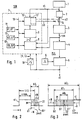
- Fig. 1 shows schematically as a block diagram an embodiment of a clock 100 according to the Invention.
- a random number generator 1 generates random numbers z 1 and delivers them via one Delay device 2 to an integrator 3.
- the integrator 3 integrates the supplied Random numbers z2, z3 which can be positive or positive and negative.
- a phase modulator 4 is fed with a random number z1 or z2 whose output is on a controllable oscillator 5 is guided, the respective phase position of the integration value pa is dependent.
- PLL Phase Locked Loop
- the ring oscillator contains a variety of taps, which can be controlled individually and deliver the system clock cl in different phases.
- the single ones Delay times correspond to only a fraction of the system cycle period, for example can a half cycle can be divided by 35 delay stages in 35 different clock phases.
- the Phase modulator 4 and oscillator 5 can also be combined with one another as in FIG. 4.
- the signal path described for generating the system clock cl is controlled by a control device 7 which influences an integrator simulation 8, a comparator 9 and a selection device 10 contains.
- the control device furthermore contains memories 11, 12, 13 for a first, second and third limit value G1, G2, G3 and possibly associated counter limit values G1 ', G2', G3 ', the Via a data bus 19 of the integrator simulation, the comparator and the selection device are feedable.
- the integrator simulation 8 it is checked whether the new random number z 1 after the integration step remains within the second or third limit values G2, G2 ', G3, G3'. For this, the Integrator simulation fed with the current integration value pa and the new random number z1 each added or subtracted according to the sign.
- the integration result j is compared in 9 with the Limit values G2, G2 ', G3, G3' are compared and the result is supplied to the selection device 10.
- This is connected to a modification device 17, which may be a modified one Random number z3, which instead of the input of the integrator 3 via an electronic switch 14 the delayed random number z2 is supplied.
- the selector 10 contains the logical ones Operations to decide whether the random number z1 should be integrated or in what way the modification has to take place so that the corresponding limit values are observed.
- FIG. 2 shows an example of a falling clock edge 21 of a system clock cl, like this clock edge can be changed in the positive or negative time direction by the individual phase steps ps.
- the minimum permissible clock phase cmin which has a lower limit value, the first limit value G1
- G1 the minimum permissible clock phase
- G1 the minimum permissible clock phase
- the phase jump that enlarges the active clock phase is this Restriction not really subject. For reasons of expediency, however, one also limits the positive phase jump to the same amount M.
- Fig. 2 shows the maximum jump + M and the associated upper limit is G1 '.
- a lounge area is defined by the boundaries G1, G1 ' A0 defines that the permissible stay area with a pure phase modulation, i.e. without Integrator 3 corresponds. If the phase jump does not start from the target phase, the Maximum jump up to the range limit G1, G1 'can be larger or smaller accordingly. In the borderline case the maximum jump goes from one area boundary to the other.
- FIG. 3 schematically shows the location area of a rising edge 22 in a first or second Time interval I1, I2 shown.
- This case is of interest if the flank is temporarily wider than in Fig. 2 can move away from the target phase pso11 without the requirement for the minimum To violate clock phase cmin.
- the limits for this location area A1 are represented by G2, G2 ', the area being different expediently extends symmetrically around the desired phase pso11. As a rule, this should Lounge area A1 may be larger than lounge area A0. The following applies at low clock frequencies this does not, compare the frequency range below 24 MHz in FIG. 7.
- FIG. 4 schematically shows an exemplary embodiment of an oscillator 5 that can be controlled in phase shown, which is designed as a ring oscillator.
- the ring oscillator contains in its ring circuit 35 successive delay stages 20, the total delay time together half the period T / 2 of the system clock cl by means of the not shown Phase control loop PLL is regulated.
- the taps at the individual delay stages are included a multiple switch 30 connected, depending on the associated integration value pa, the represents accumulated phase value, selects one of these connections and as auxiliary clock c1 ', which the has twice the frequency of the system clock cl, feeds a frequency divider 25.
- the system clock cl can be tapped by means of a driver stage, not shown is reinforced. The rising and falling edges of the system clock become the auxiliary clock modified in phase independently of each other.
- positive and negative phase steps + ps, -ps are provided, then it makes more sense not to link the reference phase to the beginning of the delay chain, but with a later tap. So the range of permissible positive and negative Phase steps are not restricted, it is also expedient to the end 36 of the Delay chain
- the attached delay chain with delay handles 37 to 53 avoids that Conversion of the original taps 0 to 35 when phase steps occur that are larger or less than this range.
- phase steps with area limits When considering the time diagram in FIG. 5, area boundaries do not yet occur.
- the relationship between phase steps with area limits is shown in FIG. 6.
- a scaling shows that accumulated phase values pa.
- the range of scaling extends asymmetrically from -8 to 23.
- the first phase step ps6, which goes over six phase increments and starts from the phase value pa 7, lies fully within the first lounge area A1.
- the one started from the same phase value Phase step ps10 would, however, come to phase value 17, which lies outside the first range A1.
- phase steps ps can be allowed, but it is a certain computational effort required.
- the largest possible resulting phase step in mirroring goes from area limit G2 to area limit G2 'or vice versa, if the permissible Maximum jump M, which results from the cmin requirement, is not exceeded.
- FIGS. 7 to 12 are examples in diagram form for areas of residence of the accumulated Phases pa are shown depending on the selected frequency of the system clock cl.
- the frequency axis is plotted with the frequencies from 0 to 50 MHz.
- a half cycle T / 2 is plotted on the left, which is the delay times corresponds to all delay stages 20 connected in the ring, for example 35 Delay stages as in Fig. 4. According to the projection on this arrow, the respective number of delay stages 20 defined.
- the line 10 ns running from D to C applies to the assumed case that the respective clock phase must be at least 10 ns long.
- the vertical Arrow on the right is also scaled with the half cycle period T / 2, but is plotted in the vertical direction the maximum permissible phase value of the first area A1.
- the line that follows therefore describes the accumulated phase value pa, which must not be exceeded so as not to violate the 12 ns range given as an example.
- the line running from D to C the limit for the accumulated phase values due to the 10 ns minimum phase range must not be exceeded.
- the possible maximum jumps M are therefore once through the connecting line A, B and the other through the connecting line B, C Are defined.
- the triangle A, B, C gives the stay area for the pure phase modulation Phase values under the given conditions, i.e. 10ns minimum phase and 12ns phase stay range, on. All phase values can be generated directly by the random number generator become.
- the connecting line DC of Fig. 7 shows that in the example shown at a low Clock frequency of 4 MHz the demand for a sufficiently long and active clock phase, the Limit defined by cmin is maintained almost throughout the half-cycle T / 2.
- the range from T / 2 to T is the inactive range is the clock phase at which the clock signal is rotated 180 degrees in phase.
- the half cycle T / 2 is very short, namely only 10.4 ns long.
- the limit value cmin 10 ns can be achieved.
- connection line AE of FIG. 7 shows that, for example, at a low clock frequency of 4 MHz the requirement to stay within the stay area with 12 ns is difficult to meet is because of the low clock frequency, the individual phase steps compared to Stay area of 12 ns become relatively large.
- the delay chain of 20 stages at T / 2 corresponds to each delay stage with a phase step of approximately 6.2 ns.
- the assumed stay range of 12 ns leaves only a single phase step without Limit exceeded too. In this case too there is a significant increase in the number of Delay stages required to reduce the gradation of the phase steps and thus one To allow variation of the clock phase.
- the resulting stay area A, B, C results from the previous considerations, the limits are determined by the more unfavorable conditions.
- the cheapest The range for the selection of the clock frequency and the number of delay stages can be from one easily find such a diagram.
- the assumed parameters of the diagram of FIG. 7 it is approximately in the middle frequency range at 24 MHz, because there the maximum permissible Phase shift M is largest, and thus also allows the greatest phase variation
- the maximum phase jump M is through the distance valid for the respective clock frequency and a pure phase modulation Range limits defined in accordance with FIG. 7 and FIG. 8.
- the there from area boundary to Phase shift reaching the boundary uses the previously explained return strategy Mirroring at the area boundary.
- the maximum possible jump distance therefore ranges from one Area boundary to the other.
- Fig. 9 shows the location diagram in a clock with an integrator according to the invention under the same requirements for the system clock as in FIGS. 7 and 8.
- FIG unsymmetrical case shown which starts from the phase reference value 0 and positive phase deviations having.
- the dashed location area A, C, E is compared to FIG. 7 around the area B, C, E got bigger.
- the conditions for the maximum jump M are through the connecting lines A, B and B, C are given.
- the arrows drawn all correspond to those for the respective frequency assigned maximum jumps.
- At 40 MHz three superimposed maximum jumps M, that the stay area there is significantly larger than the maximum jump permitted at this frequency Damn.
- the stay area A1 created by the frequency modulation is larger than that stay area A0 defined by the permissible maximum jump M
- the diagram of FIG. 10 differs from the diagram of FIG. 9 only in that that the range limits are assumed to be symmetrical about the phase reference value 0.
- Frequencies are the maximum jumps through the 6ns boundary lines running from A to B 1 and A to B1 ' limited.
- the largest maximum jump M is reached at B1, B1 'and is the same size as the maximum jump at B in FIG. 9.
- the two 5 ns boundary lines run from S to C as in FIG. 8 and S 'after C; the intersections with the lines AF and Af 'are B 1 and B1'.
- the living area A, F ', F is identical to the area A, C, E of FIG. 9.
- FIGS. 11 and 12 are partly the same as the diagrams of FIGS. 9 and 10 and contain in particular their areas of residence A, C, E or A, F ', F. They also contain Diagrams but a supplementary location area E, H, I, J and C, H ', I', J 'or F, K, L, N and F ', K', L ', N'. These areas of residence result from the fact that according to FIG. 3 or FIG. 6 An extended stay area A2 applies at least for the intended time intervals I2. By means of a single maximum jump M, however, are the limits of the 12 ns location areas A1 A, C, E and A, F, F 'reachable again.
- the associated time intervals I2 are determined, for example, from the Frequency divider 18 of FIG. 1. Starting from a relatively high-frequency system clock cl For example, data with a much lower clock rate requested via an external bus for which the relatively narrow phase boundaries of 12 ns are required. Outside of that special However, the data transfer can run the phases further away, which is the additional areas in FIG. 11 and Fig. 12 corresponds.
- the limits I, J; I ', J' or L, N; L ', N' are related to the division ratio of the divider 18, which is indicated in Figures 11 and 12 as t :. If the divider 18 is not present, then it is Division ratio 1: 1 and in every system clock cl the closer residence condition A1 be respected. Only when the division ratio is 2: 1 is an extended lounge area A2 possible for every second measure. The first bar has a narrow lounge area A1, the next a wide A2, the third again a narrow A1 etc. If, for example, to query the narrow frequency range A1 a fixed frequency of 8 MHz is specified, then the Divider 18 at most that according to the diagrams going from 0 to 50 MHz Have a 6: 1 division ratio.
- the system clock cl then has a maximum frequency of 48 MHz and the maximum phase step M is only one at 20 delay stages Phase step.
- the phase stay range however, ranges from C to almost E in FIG. 11 or in FIG. 12 almost from F 'to F.
- the block diagram of FIG. 13 shows, as a partial circuit of the control device 7, a circuit example for the sign reversal in the event of a range being exceeded.
- the random number z1 formed by the random number generator 1 is fed to an integrator simulation 8, which contains an adder / subtractor as the arithmetic unit 38.
- the computing unit 38 forms the sum or difference between the old integration value j -1 and the new random number z1.
- the result of this calculation process is a test integration value j, which is fed to the adding input of a first and a second calculation unit 42, 43 in the comparator 9.1.
- the evaluation supplies a first and second logic signal a, b, which together with a third logic signal c, which corresponds to the sign or the MSB location of the random number z1, is fed to a selection device 10.1.
- This combines the three logic signals A, B, C with a combination of an OR gate 46 and an AND gate 47, the latter having a negative input 48 for the logic signal b.
- the result of this logical combination is a fourth logic signal d, which is fed to a first subcircuit 17.1 of the modification device 17 as a control signal.
- the subcircuit 17.1 supplies the original random number z1 or the random numbers z2 delayed by the delay device 2 or another number, for example a modified random number z1, at its output as the output value k.
- the table shown in the first subcircuit 17.1 shows how the output value k is related to the original random number z1 and the control signal d. If the signal d has the logic state 0, then the output number k is a positive number, regardless of the sign of the original random number z1. If the signal d has the logic state 1, then the output number k is a negative number, regardless of the original sign of the random number z1.
- the relationship between the logic signal d and the processing of the original random number z1 is shown in detail in the table below of FIG. 14.
- the number k output by the modification subcircuit 17.1 ensures that the limits G2 ', G2 are not exceeded when this number k is integrated in the integrator 3.
- the amount of k is added to or subtracted from the previous integration value j -1 and thus forms the new integration value j ', which is available at the output of the accumulator computing unit 40.
- This new integration value is fed to an accumulator memory 41. In the next comparison phase, it then serves as the old integration value j -1 .
- the random number z1 has five digits, for example, the output the integrator simulation 8 seven digits and the outputs of the computing units 42, 43 and Evaluators 44, 45 one position each.
- the test integration value j leaves the range specified by the limit values G2, G2 '. In lines 3 and 4, however, the test integration value j remains within the predetermined limits G2 and G2 '. Lines 3 and 4 do not change the arithmetic operation to be performed in integrator 3. The original arithmetic operations result from the sign of the random number z1, see the corresponding logic signal c in column 2. From line 3 it thus follows that the positive number z1 can be added to the previous integration value j -1 and from line 4 it results that the negative number z1 can be subtracted from the previous integration value j -1 .
- the test integration value j leaves the limit values G2, G2 ' predetermined range.
- signal a therefore assumes the logic state "1".
- the signal b assumes the logical state "1" accordingly.
- the fourth logic signal b is formed by means of the gate circuits 46, 47 shown in FIG. If the limits G2, G2 'are fallen short of or exceeded, then the sign of the random number z1 be changed for integration, which shows column six.
- a change in the sign of z1 in line one or in line 2 means a negative or positive numerical value k and maintaining the sign of z1 in lines three and four means a positive or negative numerical value k.
- the desired sign of the numerical value k of Column 7 is directly correlated with the logic state of signal d from column 4, the amount of k is equal to the amount of the random number z1.
- the random number z1 are provided in positive and negative form. This can vary depending on the number system used by an inversion, complementation, a corresponding table or another procedure.
- the logic signal d then makes the positive or equal Large negative random number is read out as the output value k and fed to the integrator 3.
- Fig. 13 and the associated table in Fig. 14 excludes others Procedures for checking and modifying the random number z1 are of course not sufficient.
- the illustrated example illustrates the function of a comparator 9.1 and a subcircuit 17.1 of the modification device 17.
- the strategy for compliance with the predetermined limits on the direction reversal of the random number z1 is also compared to others Procedure very easy to implement.
- FIG. 15 Another comparator 9 is shown in FIG. 15, which checks whether the test integration value j is within of the limits G3, G3 'remains.
- the comparator device 9 with third and fourth computing unit 49, 50 and third and fourth evaluators 51, 52 corresponds to the comparator device 9 in FIG. 13.
- the associated output signals, the fifth and sixth logic signals e and f are a selection device 10.2 supplied, which links the logic signals e and f to one another via an OR gate 53.
- the output signal of this gate 53 is a seventh logic signal g as the control signal of a second one Subcircuit 17.2 of the modification device 17 is supplied.
- the signals e and f are as further Control signals m + and m- supplied to the subcircuit 17.2.
- the first and second subcircuits 17.1, 17.2 of the modification device 17 are fed with the signals a, b, c or with the signals m +, m.
- the logic signal g controls an electronic switch 55, which at its output outputs number k to be integrated. In the switch position "0" this is the initial value k
- Subcircuit 17.1 and in switch position 1 is the positive or negative maximum jump + M, -M of the subcircuit 17.2.
- Subcircuit 17.1 corresponds directly to subcircuit 17.1 of Fig. 13.
- the comparator 9.2 of FIG. 15 recognizes that the limit values G2, G2 'are exceeded, it solves the provided return strategy R, in which the random number to be integrated z1, for example, by a positive or negative maximum jump + M, -M is replaced.
- the two maximum jumps are in the simplest case, the limit values G1, G1 'specified in the memory 11. Choosing which of the two maximum jumps is carried out, the control signals determine m +, m- by one of both have the logical state "1". If neither of the two limits G2, G2 'is exceeded no maximum jump is required and both signals m +, m- are in the "0" state as well the resulting signal g.
- the switch 55 accordingly takes the switch position "0".
- the checking of all limits entails a large number of additions and subtractions, some of which run in parallel, but some of which also depend on previous arithmetic operations and thus run in series.
- the time required for the test integrations can be compensated for by the delay device 2 or a pipeline method.
- Another possibility is that separate computing units are combined to form multiple computing units, for example by including the computing unit 38 in the computing units 42 and 43, respectively.
- a further acceleration is that all arithmetic operations that occur are carried out in parallel arithmetic units and a special selection device outputs one of these arithmetic results as a new integration value.
- FIG. 16 Four multiple computing units 60 and four single computing units 70 are connected to a special selection device 80.
- the output of the selection unit 80 supplies the new integration value pa, which is then fed to the phase-controlled oscillator 5 in the clock generator 100.
- the following arithmetic operations are carried out in the arithmetic units 60, 70 connected in parallel, the random number z1 to be examined being taken into account with the correct sign, that is to say as a positive or negative numerical value.
- the following table shows the arithmetic operations to be carried out in parallel in the individual arithmetic units using the example of the sign reversal procedure: Multiple computing unit 61 j + z1 - G2 ' Multiple computing unit 62 j + z1 - G2, Multiple computing unit 63 j + z1 - G3 ', Multiple computing unit 64 j + z1 - G3, Single arithmetic unit 71 j + z1, Single computing unit 72 j - z1, Single arithmetic unit 73 j + M Single arithmetic unit 74 j - M.
Landscapes
- Engineering & Computer Science (AREA)
- Physics & Mathematics (AREA)
- Theoretical Computer Science (AREA)
- General Engineering & Computer Science (AREA)
- General Physics & Mathematics (AREA)
- Nonlinear Science (AREA)
- Computer Networks & Wireless Communication (AREA)
- Signal Processing (AREA)
- Stabilization Of Oscillater, Synchronisation, Frequency Synthesizers (AREA)
- Synchronisation In Digital Transmission Systems (AREA)
- Manipulation Of Pulses (AREA)
Abstract
Description
| Mehrfachrecheneinheit 61 | j + z1 - G2' |
| Mehrfachrecheneinheit 62 | j + z1 - G2, |
| Mehrfachrecheneinheit 63 | j + z1 - G3', |
| Mehrfachrecheneinheit 64 | j + z1 - G3, |
| Einfachrecheneinheit 71 | j + z1, |
| Einfachrecheneinheit 72 | j - z1, |
| Einfachrecheneinheit 73 | j + M |
| Einfachrecheneinheit 74 | j - M. |
- 1
- Zufallszahlengenerator
- 2
- Verzögerungseinrichtung
- 3
- Integrator
- 4
- Phasenmodulator
- 5
- phasengesteuerter Oszillator
- 6
- Referenzoszillator
- 7
- Kontrolleinrichtung
- 8
- Integratornachbildung
- 9
- Vergleicher
- 9.1/9.2
- erster/zweiter Vergleicher
- 10 /10.1/10.2
- Auswahleinrichtung
- 11,12,13
- Speicher für Grenzwerte
- 14
- elektronischer Schalter
- 17
- Modifikationseinrichtung
- 17.1 / 17.2
- erste/zweite Teilschaltung
- 19
- Datenbus
- 20
- Verzögerungsstufen
- 21
- abfallende Taktflanken
- 22
- Anstiegsflanken
- 25
- Frequenzteiler
- 30
- Vielfachschalter
- 38
- Recheneinheit der Integratornachbildung
- 40
- Akkumulator-Recheneinheit
- 41
- Akkumulator-Speicher
- 42/43
- 1./2. Recheneinheit
- 44/45
- 1./2. Bewerter
- 46
- ODER-Tor
- 47
- UND-Tor
- 48
- negierender Eingang
- 49/50
- 3./4. Recheneinheit
- 51 / 52
- 3./4. Bewerter
- 55
- elektronischer (Um-)Schalter
- 60, 61-64
- Mehrfachrecheneinheiten
- 70, 71-74
- Einfachrecheneinheiten
- 80
- Recheneinheits-Auswahleinrichtung
- 100
- Taktgeber
- A, B, B1, B1`, C, F, F`, S, S`, H, H', I, I`, J, J` K, K`, L, L`, N, N`
- Diagrammpunkte
- a, b, c, d, e, f
- Logiksignale
- A0
- reiner, phasengesteuerter Aufenthaltsbereich
- A1, A2
- 1./2. Aufenthaltsbereich
- c1, c1`
- Systemtakt, Hilfstakt
- cmin
- minimale Taktphase
- fcl
- Frequenz des Systemtaktes
- fr
- Frequenz des Ringoszillators
- g
- Steuersignal, Logiksignal
- G1,G2,G3 G1`,G2,G3`
- Grenzwerte
- I1, I2
- 1./2. Zeitintervall
- j
- Testintegrationswert
- j`
- neuer Integrationswert
- j-1
- vorausgehender Integrationswert
- k
- zu integrierende Zahl
- M, M`, M*
- Maximalsprung
- m+, m-
- Steuersignale für Maximalsprung
- pa
- Integrationswert
- PLL
- Phasenverriegelungsschleife
- ps
- Phasenschritt
- pso11
- Phasensollwert
- ps10`, ps7`
- Überschußwert
- ps6*, ps1*
- resultierender Phasenschritt
- R, +R, -R
- Rückführstrategie
- t
- Zeit
- T/2
- halbe Taktperiode
- z1
- Zufallszahl
- z2
- verzögerte Zufallszahl
- z3
- modifizierte Zufallszahl
Claims (10)
- Taktgeber (100) mit einem Zufallszahlengenerator (1) und einem Phasenmodulator (4) zur Erzeugung eines im Frequenzspektrum verschliffenen und damit störstrahlarmen Systemtaktes (c1),
gekennzeichnet durch folgende Merkmale:zwischen den Zufallszahlengenerator (1) und den Phasenmodulator (4) ist ein Integrator (3) für die vom Zufallszahlengenerator gelieferten Zufallszahlen (z1, z2) eingefügt,der Ausgang des Integrators (3) steuert über seinen Integrationswert (pa; j') den jeweiligen Phasenwert im Phasenmodulator (4) undder Integrator (3) ist mit einer Kontrolleinrichtung (7) gekoppelt, die in die Zufallszahlen (z1, z2) oder den Integrationsvorgang eingreift, um vorgegebene Grenzwerte (G1, G1'; G2, G2'; G3,G3') beim Integrationswert (pa, j') nicht zu überschreiten. - Taktgeber (100) nach Anspruch 1, dadurch gekennzeichnet, daß ein erster Grenzwert (G1, G1'; cmin) und Startwert (psoll; G1 bzw. G1'; G2 bzw. G2') einen Maximalsprung (M; M'; M*) des Integrationswertes (pa; j') vorgeben, der einem maximal zulässigen Phasensprung des Systemtaktes (c1) entspricht.
- Taktgeber (100) nach Anspruch 1, dadurch gekennzeichnet, daß ein zweiter Grenzwert (G2, G2') eine erste maximal zulässige Phasenabweichung des Systemtaktes (c1) mindestens während vorgegebener erster Zeitintervalle (I1) vorgibt.
- Taktgeber (100) nach einem der Ansprüche 1 bis 3, dadurch gekennzeichnet, daß der Zufallszahlengenerator (1) Zufallszahlen (z1, z2) erzeugt, die innerhalb eines vorgegebenen, insbesondere durch die ersten Grenzwerte (G1, G1') definierten, Wertebereiches liegen.
- Taktgeber (100) nach einem der Ansprüche 1 bis 4, dadurch gekennzeichnet, daß während zweiter Zeitintervalle (I2), die insbesondere außerhalb der ersten Zeitintervalle (I1) liegen, ein dritter Grenzwert (G3, G3') eine zweite maximal zulässige Phasenabweichung des Systemtaktes (c1) vorgibt, wobei der dritte Grenzwert betragsmäßig mindestens so groß wie der zweite Grenzwert (G2, G2') ist.
- Taktgeber (100) nach einem der Ansprüche 1 bis 5, dadurch gekennzeichnet, daß die Kontrolleinrichtung (7) mit einer Modifikationseinrichtung (17; 17.1; 17.2) gekoppelt ist, die zur Einhaltung des ersten, zweiten oder dritten Grenzwertes (G1, G1', G2, G2', G3, G3') die Zufallszahl (z1, z2) vor der Integration modifiziert.
- Taktgeber (100) nach Anspruch 6, dadurch gekennzeichnet, daß die Modifikationseinrichtung (17) eine Teilschaltung (17.2) enthält, die eine dem dritten Grenzwert (G3, G3') zugeordnete Rückführstrategie implementiert, die sicherstellt, daß spätestens zu Beginn der ersten Zeitintervalle (I1) der Integrationswert (pa; j') wieder den zweiten Grenzwert (G2, G2') einhält.
- Taktgeber (100) nach Anspruch 6 oder 7, dadurch gekennzeichnet, daß ein gegenüber dem zweiten Grenzwert (G2, G2') erweiterter Aufenthaltsbereich, der zweite Aufenthaltsbereich (A2), aus dem ersten Aufenthaltsbereich (A1) hervorgeht, indem an der oberen und/oder unteren Bereichsgrenze (G2, G2') ein Zusatzbereich angefügt ist, dessen Größe insbesondere dem Maximalsprung (M) entspricht.
- Taktgeber (100) nach einem der Ansprüche 1 bis 8, dadurch gekennzeichnet, daß mindestens ein Teil der Rechenoperationen der Kontrolleinrichtung (7) und des Integrators (3) mittels parallelgeschalteter Recheneinheiten (60, 70) erfolgt und eine Recheneinheits-Auswahlschaltung (80) einen dieser Recheneinheiten auf einen Ausgang zur Abgabe eines neuen Integrationswertes (pa; j') durchschaltet.
- Verfahren zur Erzeugung einer modifizierten Zufallszahl (z3; k), die in einem Taktgeber (100) gemäß einem der Ansprüche 1 bis 9 einem Integrator (3) anstatt einer Zufallszahl (z1, z2) zur Integration zugeführt ist, wobei in einem ersten Schritt festgestellt wird, daß mit der Zufallszahl (z1, z2) bei der Integration ein zulässiger Bereich (A0, A1, A2) überschritten wird und danach ein zweiter Schritt folgt, bei dem:die zu integrierende Zufallszahl (z1, z2) durch eine vorgegebene Zahl, die insbesondere einem vorgegebenen Maximalsprung M entspricht, ersetzt wird oderdie zu integrierende Zufallszahl (z1, z2) durch eine vorgegebene Folge von Zahlen ersetzt wird oderder Überschußwert (ps10', ps7') der zu integrierenden Zufallszahl (z1, z2) an einer zugehörigen Bereichsgrenze (G1, G1', G2, G2', G3, G3') gespiegelt wird oderdie zu integrierende Zufallszahl (z1, z2) durch eine betragsgleiche Zahl mit geändertem Vorzeichen ersetzt wird oderdie zu integrierende Zufallszahl (z1, z2) bei Überschreitung einer dritten Bereichsgrenze (G3, G3') durch eine, insbesondere dem zulässigen Maximalsprung (M) entsprechende, vorgegebene Zahl mit passendem Vorzeichen, welche die Rückkehr in zweite Bereichsgrenzen (G2, G2') spätestens zu Beginn eines ersten Zeitintervalls (I1) ermöglicht, ersetzt wird oderdie zu integrierende Zufallszahl (z1, z2) oder einer Folge der letzten Zufallszahlen durch eine Wiederholung der Zufallszahl oder der Folge der letzten Zufallszahlen mit Änderung mindestens eines Vorzeichens, wobei die Reihenfolge bei der Wiederholung beliebig ist, ersetzt wird oderdie zu integrierende Zufallszahl (z1, z2) unterdrückt wird und solange neue Zufallszahlen erzeugt werden, bis eine passende Zufallszahl vorliegt, mit der die jeweiligen Bereichsgrenzen eingehalten werden.
Priority Applications (2)
| Application Number | Priority Date | Filing Date | Title |
|---|---|---|---|
| JP2001387392A JP3902464B2 (ja) | 2000-12-23 | 2001-12-20 | 周波数ジッターシステムクロックを発生するためのクロック発生器 |
| US10/033,719 US20020138780A1 (en) | 2000-12-23 | 2001-12-26 | Clock generator for generating a frequency-jittered system clock |
Applications Claiming Priority (2)
| Application Number | Priority Date | Filing Date | Title |
|---|---|---|---|
| DE10065072A DE10065072C1 (de) | 2000-12-23 | 2000-12-23 | Taktgeber zur Erzeugung eines im Frequenzspektrum verschliffenen Systemtaktes |
| DE10065072 | 2000-12-23 |
Publications (3)
| Publication Number | Publication Date |
|---|---|
| EP1217498A2 true EP1217498A2 (de) | 2002-06-26 |
| EP1217498A3 EP1217498A3 (de) | 2006-10-18 |
| EP1217498B1 EP1217498B1 (de) | 2007-05-30 |
Family
ID=7669026
Family Applications (1)
| Application Number | Title | Priority Date | Filing Date |
|---|---|---|---|
| EP01106972A Expired - Lifetime EP1217498B1 (de) | 2000-12-23 | 2001-03-21 | Taktgeber zur Erzeugung eines im Frequenzspektrum verschliffenen Systemtaktes |
Country Status (3)
| Country | Link |
|---|---|
| EP (1) | EP1217498B1 (de) |
| AT (1) | ATE363681T1 (de) |
| DE (2) | DE10065072C1 (de) |
Family Cites Families (3)
| Publication number | Priority date | Publication date | Assignee | Title |
|---|---|---|---|---|
| DE4442403C2 (de) * | 1994-11-30 | 1997-01-23 | Itt Ind Gmbh Deutsche | Taktgenerator zur Erzeugung eines störstrahlarmen Systemtaktes |
| DE19517265A1 (de) * | 1995-05-11 | 1996-11-14 | Vdo Schindling | Verfahren und Schaltungsanordnung zur Verringerung von Störungen |
| FR2766308B1 (fr) * | 1997-07-18 | 2001-05-11 | Peugeot | Procede pour attenuer les effets des emissions electromagnetiques parasites produites par un signal de commande |
-
2000
- 2000-12-23 DE DE10065072A patent/DE10065072C1/de not_active Expired - Lifetime
-
2001
- 2001-03-21 AT AT01106972T patent/ATE363681T1/de not_active IP Right Cessation
- 2001-03-21 DE DE50112556T patent/DE50112556D1/de not_active Expired - Lifetime
- 2001-03-21 EP EP01106972A patent/EP1217498B1/de not_active Expired - Lifetime
Also Published As
| Publication number | Publication date |
|---|---|
| ATE363681T1 (de) | 2007-06-15 |
| DE10065072C1 (de) | 2002-06-13 |
| DE50112556D1 (de) | 2007-07-12 |
| EP1217498A3 (de) | 2006-10-18 |
| EP1217498B1 (de) | 2007-05-30 |
Similar Documents
| Publication | Publication Date | Title |
|---|---|---|
| DE69018023T2 (de) | Phasenverriegelschleife mit variabler Bandbreite. | |
| DE69017129T2 (de) | Frequenzsynthesizer mit gebrochenem teilverhältnis. | |
| DE102016109077A1 (de) | Verfahren zum Betreiben eines modularen Multilevelkonverters | |
| DE60002233T2 (de) | Phasenregelkreis und Frequenzmodulationsverfahren zu dessen Nutzung | |
| DE3205247C2 (de) | ||
| DE102004052416B4 (de) | Regelkreisfilter | |
| DE10196304B4 (de) | Variable Verzögerungsschaltung | |
| DE4406300C2 (de) | Lineares Interpolationsverfahren | |
| DE102005018858B4 (de) | Digitales Filter und Verfahren zur Bestimmung seiner Koeffizienten | |
| EP1217498B1 (de) | Taktgeber zur Erzeugung eines im Frequenzspektrum verschliffenen Systemtaktes | |
| EP1513249A1 (de) | Verfahren zur Symmetrierung eines Gleichspannungskreises einer Umrichterschaltung zur Schaltung von drei Spannungsniveaus | |
| DE3601858C1 (de) | Schaltungsanordnung zur Frequenzteilung | |
| DE102004001030B4 (de) | Verschachtelte Hochauflösungsverzögerungskette | |
| EP0406693A2 (de) | Verfahren zum Filtern digitalisierter Signale | |
| DE3843261A1 (de) | Schaltungsanordnung zur steuerung der phase eines taktsignals | |
| DE69615536T2 (de) | Mos transistor | |
| EP1101162B1 (de) | Verfahren und vorrichtung zur erzeugung von taktsignalen | |
| EP1095284B1 (de) | Schaltung zur ermittlung der zeitdifferenz zwischen flanken eines ersten und eines zweiten digitalen signals | |
| DE602005004652T2 (de) | Signal Generator | |
| DE102004052418B4 (de) | Gewichtungsschaltung und Verfahren zum Einregeln eines Regelkreises | |
| DE10140485C2 (de) | Verfahren und Vorrichtung zur Frequenzerzeugung | |
| DE10009451C1 (de) | Recheneinheit für eingeschränkte Signalverarbeitung | |
| DE4136980A1 (de) | Vorrichtung zur veraenderung des tastverhaeltnisses oder der pulszahldichte einer signalfolge | |
| DE10148542A1 (de) | Verfahren zur Bestimmung von periodisch stationären Lösungen eines technischen Systems | |
| DE10163350A1 (de) | Verfahren und Vorrichtung zum Erzeugen eines Ausgangssignals als mathematische Funktion eines Eingangssignals |
Legal Events
| Date | Code | Title | Description |
|---|---|---|---|
| PUAI | Public reference made under article 153(3) epc to a published international application that has entered the european phase |
Free format text: ORIGINAL CODE: 0009012 |
|
| AK | Designated contracting states |
Kind code of ref document: A2 Designated state(s): AT BE CH CY DE DK ES FI FR GB GR IE IT LI LU MC NL PT SE TR |
|
| AX | Request for extension of the european patent |
Free format text: AL;LT;LV;MK;RO;SI |
|
| PUAL | Search report despatched |
Free format text: ORIGINAL CODE: 0009013 |
|
| AK | Designated contracting states |
Kind code of ref document: A3 Designated state(s): AT BE CH CY DE DK ES FI FR GB GR IE IT LI LU MC NL PT SE TR |
|
| AX | Request for extension of the european patent |
Extension state: AL LT LV MK RO SI |
|
| 17P | Request for examination filed |
Effective date: 20061026 |
|
| GRAP | Despatch of communication of intention to grant a patent |
Free format text: ORIGINAL CODE: EPIDOSNIGR1 |
|
| GRAS | Grant fee paid |
Free format text: ORIGINAL CODE: EPIDOSNIGR3 |
|
| GRAA | (expected) grant |
Free format text: ORIGINAL CODE: 0009210 |
|
| AK | Designated contracting states |
Kind code of ref document: B1 Designated state(s): AT BE CH CY DE DK ES FI FR GB GR IE IT LI LU MC NL PT SE TR |
|
| PG25 | Lapsed in a contracting state [announced via postgrant information from national office to epo] |
Ref country code: FI Free format text: LAPSE BECAUSE OF FAILURE TO SUBMIT A TRANSLATION OF THE DESCRIPTION OR TO PAY THE FEE WITHIN THE PRESCRIBED TIME-LIMIT Effective date: 20070530 |
|
| REG | Reference to a national code |
Ref country code: GB Ref legal event code: FG4D Free format text: NOT ENGLISH |
|
| AKX | Designation fees paid |
Designated state(s): AT BE CH CY DE DK ES FI FR GB GR IE IT LI LU MC NL PT SE TR |
|
| REG | Reference to a national code |
Ref country code: CH Ref legal event code: EP |
|
| GBT | Gb: translation of ep patent filed (gb section 77(6)(a)/1977) |
Effective date: 20070613 |
|
| REG | Reference to a national code |
Ref country code: IE Ref legal event code: FG4D Free format text: LANGUAGE OF EP DOCUMENT: GERMAN |
|
| REF | Corresponds to: |
Ref document number: 50112556 Country of ref document: DE Date of ref document: 20070712 Kind code of ref document: P |
|
| PG25 | Lapsed in a contracting state [announced via postgrant information from national office to epo] |
Ref country code: SE Free format text: LAPSE BECAUSE OF FAILURE TO SUBMIT A TRANSLATION OF THE DESCRIPTION OR TO PAY THE FEE WITHIN THE PRESCRIBED TIME-LIMIT Effective date: 20070830 |
|
| PG25 | Lapsed in a contracting state [announced via postgrant information from national office to epo] |
Ref country code: ES Free format text: LAPSE BECAUSE OF FAILURE TO SUBMIT A TRANSLATION OF THE DESCRIPTION OR TO PAY THE FEE WITHIN THE PRESCRIBED TIME-LIMIT Effective date: 20070910 |
|
| ET | Fr: translation filed | ||
| REG | Reference to a national code |
Ref country code: IE Ref legal event code: FD4D |
|
| PG25 | Lapsed in a contracting state [announced via postgrant information from national office to epo] |
Ref country code: IE Free format text: LAPSE BECAUSE OF FAILURE TO SUBMIT A TRANSLATION OF THE DESCRIPTION OR TO PAY THE FEE WITHIN THE PRESCRIBED TIME-LIMIT Effective date: 20070530 Ref country code: DK Free format text: LAPSE BECAUSE OF FAILURE TO SUBMIT A TRANSLATION OF THE DESCRIPTION OR TO PAY THE FEE WITHIN THE PRESCRIBED TIME-LIMIT Effective date: 20070530 Ref country code: PT Free format text: LAPSE BECAUSE OF FAILURE TO SUBMIT A TRANSLATION OF THE DESCRIPTION OR TO PAY THE FEE WITHIN THE PRESCRIBED TIME-LIMIT Effective date: 20071030 |
|
| PLBE | No opposition filed within time limit |
Free format text: ORIGINAL CODE: 0009261 |
|
| STAA | Information on the status of an ep patent application or granted ep patent |
Free format text: STATUS: NO OPPOSITION FILED WITHIN TIME LIMIT |
|
| PG25 | Lapsed in a contracting state [announced via postgrant information from national office to epo] |
Ref country code: GR Free format text: LAPSE BECAUSE OF FAILURE TO SUBMIT A TRANSLATION OF THE DESCRIPTION OR TO PAY THE FEE WITHIN THE PRESCRIBED TIME-LIMIT Effective date: 20070831 |
|
| 26N | No opposition filed |
Effective date: 20080303 |
|
| BERE | Be: lapsed |
Owner name: MICRONAS G.M.B.H. Effective date: 20080331 |
|
| PG25 | Lapsed in a contracting state [announced via postgrant information from national office to epo] |
Ref country code: MC Free format text: LAPSE BECAUSE OF NON-PAYMENT OF DUE FEES Effective date: 20080331 |
|
| REG | Reference to a national code |
Ref country code: CH Ref legal event code: PL |
|
| PG25 | Lapsed in a contracting state [announced via postgrant information from national office to epo] |
Ref country code: LI Free format text: LAPSE BECAUSE OF NON-PAYMENT OF DUE FEES Effective date: 20080331 Ref country code: CH Free format text: LAPSE BECAUSE OF NON-PAYMENT OF DUE FEES Effective date: 20080331 |
|
| PG25 | Lapsed in a contracting state [announced via postgrant information from national office to epo] |
Ref country code: BE Free format text: LAPSE BECAUSE OF NON-PAYMENT OF DUE FEES Effective date: 20080331 |
|
| PG25 | Lapsed in a contracting state [announced via postgrant information from national office to epo] |
Ref country code: CY Free format text: LAPSE BECAUSE OF FAILURE TO SUBMIT A TRANSLATION OF THE DESCRIPTION OR TO PAY THE FEE WITHIN THE PRESCRIBED TIME-LIMIT Effective date: 20070530 |
|
| PG25 | Lapsed in a contracting state [announced via postgrant information from national office to epo] |
Ref country code: AT Free format text: LAPSE BECAUSE OF NON-PAYMENT OF DUE FEES Effective date: 20080321 |
|
| PG25 | Lapsed in a contracting state [announced via postgrant information from national office to epo] |
Ref country code: LU Free format text: LAPSE BECAUSE OF NON-PAYMENT OF DUE FEES Effective date: 20080321 |
|
| PG25 | Lapsed in a contracting state [announced via postgrant information from national office to epo] |
Ref country code: TR Free format text: LAPSE BECAUSE OF FAILURE TO SUBMIT A TRANSLATION OF THE DESCRIPTION OR TO PAY THE FEE WITHIN THE PRESCRIBED TIME-LIMIT Effective date: 20070530 |
|
| PGFP | Annual fee paid to national office [announced via postgrant information from national office to epo] |
Ref country code: NL Payment date: 20100315 Year of fee payment: 10 Ref country code: IT Payment date: 20100327 Year of fee payment: 10 |
|
| REG | Reference to a national code |
Ref country code: NL Ref legal event code: V1 Effective date: 20111001 |
|
| PG25 | Lapsed in a contracting state [announced via postgrant information from national office to epo] |
Ref country code: NL Free format text: LAPSE BECAUSE OF NON-PAYMENT OF DUE FEES Effective date: 20111001 |
|
| PG25 | Lapsed in a contracting state [announced via postgrant information from national office to epo] |
Ref country code: IT Free format text: LAPSE BECAUSE OF NON-PAYMENT OF DUE FEES Effective date: 20110321 |
|
| REG | Reference to a national code |
Ref country code: FR Ref legal event code: PLFP Year of fee payment: 15 |
|
| REG | Reference to a national code |
Ref country code: FR Ref legal event code: PLFP Year of fee payment: 16 |
|
| REG | Reference to a national code |
Ref country code: DE Ref legal event code: R081 Ref document number: 50112556 Country of ref document: DE Owner name: TDK-MICRONAS GMBH, DE Free format text: FORMER OWNER: MICRONAS GMBH, 79108 FREIBURG, DE |
|
| REG | Reference to a national code |
Ref country code: FR Ref legal event code: PLFP Year of fee payment: 17 |
|
| PGFP | Annual fee paid to national office [announced via postgrant information from national office to epo] |
Ref country code: DE Payment date: 20170322 Year of fee payment: 17 Ref country code: FR Payment date: 20170322 Year of fee payment: 17 |
|
| PGFP | Annual fee paid to national office [announced via postgrant information from national office to epo] |
Ref country code: GB Payment date: 20170322 Year of fee payment: 17 |
|
| REG | Reference to a national code |
Ref country code: FR Ref legal event code: CD Owner name: TDK-MICRONAS GMBH, DE Effective date: 20180717 |
|
| REG | Reference to a national code |
Ref country code: DE Ref legal event code: R119 Ref document number: 50112556 Country of ref document: DE |
|
| GBPC | Gb: european patent ceased through non-payment of renewal fee |
Effective date: 20180321 |
|
| PG25 | Lapsed in a contracting state [announced via postgrant information from national office to epo] |
Ref country code: DE Free format text: LAPSE BECAUSE OF NON-PAYMENT OF DUE FEES Effective date: 20181002 |
|
| PG25 | Lapsed in a contracting state [announced via postgrant information from national office to epo] |
Ref country code: GB Free format text: LAPSE BECAUSE OF NON-PAYMENT OF DUE FEES Effective date: 20180321 |
|
| PG25 | Lapsed in a contracting state [announced via postgrant information from national office to epo] |
Ref country code: FR Free format text: LAPSE BECAUSE OF NON-PAYMENT OF DUE FEES Effective date: 20180331 |