EP1213769A2 - Thin film transistor and method for manufacturing the same - Google Patents
Thin film transistor and method for manufacturing the same Download PDFInfo
- Publication number
- EP1213769A2 EP1213769A2 EP01305976A EP01305976A EP1213769A2 EP 1213769 A2 EP1213769 A2 EP 1213769A2 EP 01305976 A EP01305976 A EP 01305976A EP 01305976 A EP01305976 A EP 01305976A EP 1213769 A2 EP1213769 A2 EP 1213769A2
- Authority
- EP
- European Patent Office
- Prior art keywords
- thin film
- grains
- film transistor
- crystal
- semiconductor film
- Prior art date
- Legal status (The legal status is an assumption and is not a legal conclusion. Google has not performed a legal analysis and makes no representation as to the accuracy of the status listed.)
- Ceased
Links
Images




Classifications
-
- H—ELECTRICITY
- H10—SEMICONDUCTOR DEVICES; ELECTRIC SOLID-STATE DEVICES NOT OTHERWISE PROVIDED FOR
- H10D—INORGANIC ELECTRIC SEMICONDUCTOR DEVICES
- H10D30/00—Field-effect transistors [FET]
- H10D30/01—Manufacture or treatment
- H10D30/021—Manufacture or treatment of FETs having insulated gates [IGFET]
- H10D30/031—Manufacture or treatment of FETs having insulated gates [IGFET] of thin-film transistors [TFT]
- H10D30/0312—Manufacture or treatment of FETs having insulated gates [IGFET] of thin-film transistors [TFT] characterised by the gate electrodes
- H10D30/0314—Manufacture or treatment of FETs having insulated gates [IGFET] of thin-film transistors [TFT] characterised by the gate electrodes of lateral top-gate TFTs comprising only a single gate
-
- H—ELECTRICITY
- H10—SEMICONDUCTOR DEVICES; ELECTRIC SOLID-STATE DEVICES NOT OTHERWISE PROVIDED FOR
- H10P—GENERIC PROCESSES OR APPARATUS FOR THE MANUFACTURE OR TREATMENT OF DEVICES COVERED BY CLASS H10
- H10P14/00—Formation of materials, e.g. in the shape of layers or pillars
- H10P14/20—Formation of materials, e.g. in the shape of layers or pillars of semiconductor materials
-
- H—ELECTRICITY
- H10—SEMICONDUCTOR DEVICES; ELECTRIC SOLID-STATE DEVICES NOT OTHERWISE PROVIDED FOR
- H10D—INORGANIC ELECTRIC SEMICONDUCTOR DEVICES
- H10D30/00—Field-effect transistors [FET]
- H10D30/01—Manufacture or treatment
- H10D30/021—Manufacture or treatment of FETs having insulated gates [IGFET]
- H10D30/031—Manufacture or treatment of FETs having insulated gates [IGFET] of thin-film transistors [TFT]
- H10D30/0321—Manufacture or treatment of FETs having insulated gates [IGFET] of thin-film transistors [TFT] comprising silicon, e.g. amorphous silicon or polysilicon
-
- H—ELECTRICITY
- H10—SEMICONDUCTOR DEVICES; ELECTRIC SOLID-STATE DEVICES NOT OTHERWISE PROVIDED FOR
- H10D—INORGANIC ELECTRIC SEMICONDUCTOR DEVICES
- H10D30/00—Field-effect transistors [FET]
- H10D30/60—Insulated-gate field-effect transistors [IGFET]
- H10D30/67—Thin-film transistors [TFT]
- H10D30/6729—Thin-film transistors [TFT] characterised by the electrodes
- H10D30/673—Thin-film transistors [TFT] characterised by the electrodes characterised by the shapes, relative sizes or dispositions of the gate electrodes
- H10D30/6731—Top-gate only TFTs
-
- H—ELECTRICITY
- H10—SEMICONDUCTOR DEVICES; ELECTRIC SOLID-STATE DEVICES NOT OTHERWISE PROVIDED FOR
- H10D—INORGANIC ELECTRIC SEMICONDUCTOR DEVICES
- H10D30/00—Field-effect transistors [FET]
- H10D30/60—Insulated-gate field-effect transistors [IGFET]
- H10D30/67—Thin-film transistors [TFT]
- H10D30/674—Thin-film transistors [TFT] characterised by the active materials
- H10D30/6741—Group IV materials, e.g. germanium or silicon carbide
- H10D30/6743—Silicon
- H10D30/6745—Polycrystalline or microcrystalline silicon
-
- Y—GENERAL TAGGING OF NEW TECHNOLOGICAL DEVELOPMENTS; GENERAL TAGGING OF CROSS-SECTIONAL TECHNOLOGIES SPANNING OVER SEVERAL SECTIONS OF THE IPC; TECHNICAL SUBJECTS COVERED BY FORMER USPC CROSS-REFERENCE ART COLLECTIONS [XRACs] AND DIGESTS
- Y10—TECHNICAL SUBJECTS COVERED BY FORMER USPC
- Y10S—TECHNICAL SUBJECTS COVERED BY FORMER USPC CROSS-REFERENCE ART COLLECTIONS [XRACs] AND DIGESTS
- Y10S438/00—Semiconductor device manufacturing: process
- Y10S438/969—Simultaneous formation of monocrystalline and polycrystalline regions
Definitions
- the present invention relates to a thin film transistor, particularly to one using low-temperature polycrystalline silicon, flat panel display devices using such a thin film transistor, such as liquid crystal display device and electron luminescence display device, and a method of manufacturing them.
- thin film transistor devices used for flat panel displays have been manufactured, as for instance described in (1) '99 Latest Liquid Crystal Processing Techniques (Nikkei BP, 1999), pp. 53-59 (especially page 54), by forming an amorphous silicon film on a glass substrate by PE-CVD (plasma enhanced chemical vapor deposition), subjecting this amorphous silicon film to dehydration annealing for reducing hydrogen contained in the film, and then further subjecting it to excimer laser annealing to make the film polycrystalline.
- PE-CVD plasma enhanced chemical vapor deposition
- an oxide film is formed on an amorphous silicon film after cleaning this silicon film with an ozone-containing solution, then the oxide film is removed with a fluoric acid solution, and thereafter the silicon film is subjected to laser annealing to obtain a polycrystalline silicon film free of or minimized in surface protrusions. Any of these polycrystalline silicon films, however, fell short of providing a satisfactory result.
- An object of the present invention is to provide a thin film transistor making use of a polycrystalline silicon film provided with high electron mobility and reliability by suppressing the formation of protrusions at the grain boundaries.
- the present invention provides a thin film transistor comprising a semiconductor thin film formed on a substrate, said semiconductor film being composed of a plurality of crystal grains and having present at least partly therein the clusters of grains, or the aggregates of at least two of said crystal grains.
- the present invention also provides a thin film transistor comprising, laminated on a substrate, a thin semiconductor film, a channel, an insulator film, a gate electrode, a source electrode and a drain electrode, wherein said source and drain are connected to a source region and a drain region, respectively, provided at least in a region of said semiconductor film with said channel interposed therebetween, and said semiconductor film has present at least partly therein the clusters of grains, which were formed by the aggregation of two or more of the crystal grains having (111) preferred orientation in the direction substantially parallel to the substrate surface.
- the present invention further provides a method of manufacturing a thin film transistor comprising the steps of forming a thin film of an amorphous semiconductor on a substrate, and subjecting the film to laser irradiation for heating it, wherein said laser irradiation is conducted a plural number of times to form clusters of crystal grains in at least part of said amorphous film.
- the amorphous silicon film When the amorphous silicon film is crystallized by laser annealing, the crystals do not grow up to a sufficient size, with the maximum grain size of polycrystalline silicon film after crystallization being not greater than 100 nm, if the laser irradiation energy density is small.
- the present invention has for its object to solve the above problems and to provide a high reliability thin film transistor making use of a polycrystalline silicon film having high electron mobility and reliability, realized by drastically suppressing the formation of protrusions at the grain boundaries, and a method of manufacturing such a thin film transistor.
- the above object of the present invention can be attained by forming a thin semiconductor film on a substrate, said semiconductor film being composed of a plurality of crystal grains with a size of not greater than 500 nm, and treating the film to form the clusters of grains, or the aggregates of two or more of crystal grains, at least partly in said film.
- the crystal grains are composed of Si, Ge or SiGe, and in the clusters consisting of such crystal grains, the individual grains have the same crystal orientation in the area where the individual grains adjoin each other, so that although there apparently exist the grain boundaries, it is possible to produce the substantially same characteristics as shown by the single crystals.
- the crystal orientation of the individual grains composing the clusters is identified by the transmission electron microscopical (TEM) observation of crystal lattice pattern or by the observation of electron backscattering diffraction (EBSD) pattern.
- TEM transmission electron microscopical
- EBSD electron backscattering diffraction
- the present invention provides a thin semiconductor film characterized in that the film has said clusters present at least partly therein, and that the average film thickness is 10 to 100 nm.
- the present invention is further characterized by the fact that it is possible to adopt the X-ray diffraction intensity ratio as an index of preferred orientation, and that the ratio of X-ray diffraction intensity of (111) plane to that of (220) plane, as measured by X-ray diffraction of the planes parallel to the substrate surface, is 5 or greater.
- the present invention is also typified in that the surface roughness (Rmax) of the film is 30 nm or less, with the standard deviation (RMS) thereof being 10 nm or less, and the protrusions at the grain boundaries are reduced.
- Rmax surface roughness
- RMS standard deviation
- the average electron mobility of the semiconductor film is 200 cm 2 /V ⁇ s or above.
- the clusters of grains, or the aggregates of two or more of crystal grains having (111) preferred orientation in the direction parallel to the substrate surface are allowed to exist in said film.
- the crystalline semiconductor film having said clusters of grains therein can be obtained from a process which comprises forming an amorphous semiconductor film on a substrate and laser irradiating this amorphous film a pertinent number of times to crystallize at least part of the film. It is possible to form a crystalline semiconductor film having preferred crystal orientation and suppressed in formation of protrusions at the grain boundaries.
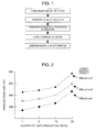
- FIG. 1 is a flow chart of the process for forming a thin polycrystalline silicon film embodying the present invention. Although the explanation is here limited to the process for forming a thin silicon film, the same process can be applied for forming a similar thin film of germanium or a silicon-germanium compound.
- a silicon nitride film (50 nm thick) is formed on a glass substrate (Corning 7059 glass is here used as substrate) by plasma enhanced chemical vapor deposition (plasma CVD).
- plasma CVD plasma enhanced chemical vapor deposition
- a silicon oxide film (100 nm thick)
- an amorphous silicon film (50 nm thick)
- the thus formed thin films on the substrate are subjected to annealing, for instance, in a 450°C furnace for 30 minutes, for dehydrogenation of the amorphous silicon film.
- the dehydrogenated amorphous silicon film is crystallized by applying, for instance, XeCl excimer laser (wavelength: 308 nm) to the film.
- Energy density of laser light used in the instant embodiment is 300 to 500 mJ/cm 2 .
- laser irradiation is conducted a plural number of times on a same part of the amorphous silicon film to crystallize it.
- "a plural number of times of laser irradiation” was conducted according to the formula in which after first laser irradiation, the amorphous silicon film is scanned by laser light at predetermined intervals, and then again laser irradiation is carried out, with these steps being repeated a desired number of times.
- the same part of the amorphous silicon film substantially undergoes a plural number of times of laser irradiation.
- the actual number of times of laser irradiation, laser beam width, laser scanning width, etc., are properly selected depending on the purpose of use of the product.
- the laser beam width is 600 ⁇ m and its scanning width is 30 ⁇ m, then the number of times of laser irradiation on the same part of the amorphous silicon film is 20.
- FIG. 2 shows the results of crystallization of an amorphous silicon film by laser irradiation conducted by changing the number of times of irradiation within the range of 1 to 20 times while varying laser energy density within the range of 300 to 500 mJ/cm 2 .
- the number of times of laser irradiation is plotted as abscissa and the average grain size in the region where laser irradiation was conducted a predetermined number of times is plotted as ordinate.
- Grain size was determined by the scanning electron microscopical observation, a well known method in the art. Specifically, the major and minor axes of the grains were measured from the SEM image, and the mean value was defined as grain size.
- the surface of the polycrystalline silicon film, which has previously been crystallized is subjected to light etching using a fluoric acid solution.
- the average grain size all of the grains with their sizes falling within the range of 10 ⁇ m ⁇ 10 ⁇ m were observed and the sizes of the individual grains were measured, with the average value of measurements being defined as average grain size under the specified laser irradiation conditions.
- the average grain size is approximately 150 nm after only one laser irradiation, while the average grain size increases to 450 nm after 20 times of laser irradiation, which indicates that the average grain size enlarges remarkably with the increase of the number of times of laser irradiation.
- the laser energy density is 400 mJ/cm 2 or 500 mJ/cm 2 .
- the average grain size is approximately 450 nm, which is almost equal to the average grain size obtained when laser irradiation is carried out 20 times at a laser energy density of 300 mJ/cm 2 .
- crystal grains of the same degree of size greatly differ from each other in crystallographic, physical and electrical properties as discussed later.
- the number of times of laser irradiation, varied in the range of 1 to 20 times, is plotted as abscissa.
- laser energy density was changed in the range of 300 to 500 mJ/cm 2 .
- Surface configuration of the crystalline thin films was measured in the area of 20 ⁇ m ⁇ 20 ⁇ m at the arbitrary points of the samples produced under the respective conditions. The maximum unevenness in the above measuring area was expressed as Rmax for an index of roughness, and it was plotted as ordinate.
- Rmax after one laser irradiation at a laser energy density of 300 mJ/cm 2 was approximately 20 nm, and this value was almost independent of the number of times of laser irradiation. It was also found that even when the laser energy density was raised to 400 mJ/cm 2 or 500 mJ/cm 2 , Rmax remained almost independent of the number of times of laser irradiation although the absolute value of surface roughness increased.
- Rmax is approximately 50 nm after one irradiation and approximately 45 nm after 20 times of irradiation.
- Rmax is approximately 70 nm after one irradiation and still about 65 nm even after 20 times of irradiation.
- average grain size is substantially same - approximately 450 nm - in both cases, but surface roughness (Rmax) differs greatly between the two cases, that is, Rmax is about 18 nm in the case of the former irradiation conditions whereas it is 65 nm in the case of the latter irradiation conditions.
- FIGS. 4A and 4B are the SEM photographs of the polycrystalline silicon film surface after laser irradiation at a laser energy density of 300 mJ/cm 2
- FIGS. 5A and 5B are the similar images after laser irradiation at a laser energy density of 500 mJ/cm 2
- FIGS. 4A and 5A show the results after one irradiation
- FIGS. 4B and 5B show the results after 20 times of irradiation.
- FIG. 6 shows the result of measurement by X-ray diffraction of the laser irradiation region.
- laser irradiation was carried out 20 times at an energy density of 300 mJ/cm 2 to crystallize the amorphous silicon film.
- the ratio of diffraction intensity at the plane (111) to that at the plane (220) was defined as crystal orientation index.
- this crystal orientation index is about 1.8 when the polycrystalline silicon film has a perfect random orientation. The greater the value of this index, the more the crystal is oriented on the plane (111).
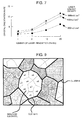
- FIG. 7 illustrates the relation between laser irradiation conditions (energy density and number of times of irradiation) and crystal orientation index.
- the crystal orientation index representing the (111)/(220) diffraction intensity ratio has a value approximate to random orientation.
- the (111) crystal orientation index begins to rise sharply. The same tendency is seen when using laser light having other energy densities.
- the crystal orientation index becomes greater when irradiation is conducted 20 times with laser light having an energy density of 300 mJ/cm 2 than when conducting irradiation only once with laser light having a higher energy density such as 400 mJ/cm 2 or 500 mJ/cm 2 . That is, in the former case, it is possible to realize a higher degree of (111) crystal orientation.
- the crystal orientation index was 6, 10 and 12 for the laser energy densities of 300 mJ/cm 2 , 400 mJ/cm 2 and 500 mJ/cm 2 , respectively.
- Observation of the crystal lattice pattern by transmission electron microscropy is an effective means for confirming that the crystal grains are caused to aggregate and grow up into clusters by a plural number of times of laser irradiation.
- FIG. 8 is a cross-sectional transmission electron micrograph of the boundary portion where the grains congregate in a polycrystalline silicon film after 20 times of irradiation with laser light having an energy density of 300 mJ/cm 2 .
- the size of the clusters is approximately 500 nm.
- grain A and grain B adjoin each other with the same crystal orientation at the boundary portion.
- the clusters formed by the aggregation of at least two grains by a plural number of times of irradiation with laser light having a predetermined energy density have substantially the same properties as the single crystals.
- FIG. 9 illustrates the result of evaluation of crystallographic orientation of the laser irradiated polycrystalline silicon film by the electron backscattering diffraction method well known in the art.
- This electron backscattering diffraction method is a method in which electron beams focused to approximately 100 nm are applied to the object of measurement, and the crystallographic orientation of the object is determined by detecting the diffracted beams from the object. Since the diameter of the electron beams applied is around 100 nm, this method is capable of analyzing the crystal orientation of the individual grains in the crystal surface.
- FIG. 9 the result of measurement by electron backscattering diffraction on the substantially same region as shown in FIG. 4B is schematically illustrated.
- the portions enclosed by the bold lines are the clusters (indicated by cluster A, cluster B, etc.) in which a plurality of small-sized grains (indicated by a1, a2, etc.) aggregate.
- the parts indicated by the fine lines in the clusters are the boundaries of the adjoining grains.
- the crystal grains were examined closely by the said electron backscattering diffraction method, and the grains having the same crystallographic orientation were marked with the same sign for discrimination from the others. As a result, it was found that although the polycrystalline silicon film is composed of the clusters having various patterns of crystal orientation, all of the individual grains composing a cluster show the same orientation, and although the grain boundaries exist, the clusters themselves possess substantially the same properties as the single crystals.
- Corning 7059 glass was used as substrate, but it is possible to use transparent substrates made of other materials such as quartz or poly(ethylene terephthalate) (PET).
- transparent substrates made of other materials such as quartz or poly(ethylene terephthalate) (PET).
- PET poly(ethylene terephthalate)
- an amorphous silicon film is formed by plasma CVD and this film is subjected to furnace annealing at an ambient temperature of 450°C to dehydrogenate the film, but this amorphous silicon film can be formed by other methods such as low pressure chemical vapor deposition (LPCVD), sputtering and evaporation.
- LPCVD low pressure chemical vapor deposition
- the film material is not limited to silicon; mixtures containing at least silicon or germanium can be used as well.
- XeCl excimer laser (wavelength: 308 nm) used in the instant embodiment is not the only means for crystallization; it is possible to use other types of excimer laser such as KrF laser (wavelength: 248 nm), YAG laser and Ar laser.
- FIG. 10 is a schematic sectional view showing the epitome of a thin film transistor comprising a glass substrate 11 and laminated thereon successively a first ground layer 12, a second ground layer 13, a semiconductor silicon layer 14, an insulating layer 15, a gate electrode layer 16, an insulating layer 17, contact holes 18 and electrodes 19.
- a silicon nitride film 12 (50 nm thick) is formed as the first ground layer on a Corning 7059 glass substrate by plasma CVD well known in the art.
- a silicon oxide film 13 (100 nm thick) as the second ground layer by plasma CVD.
- an amorphous silicon film 14 (50 nm thick), also by plasma CVD.
- the glass substrate may be a transparent substrate made of quartz, PET (poly(ethylene terephthalate)) or the like.
- the amorphous silicon film 14 may be formed by other methods such as LPCVD, sputtering or evaporation.
- the glass substrate 11 having the amorphous silicon film 14 formed thereon is subjected to furnace annealing at 450°C for 30 minutes to dehydrogenate the film.
- furnace annealing was carried out in a nitrogen atmosphere.
- the amorphous silicon film 14 is crystallized by XeCl excimer laser (wavelength: 308 nm, pulse width: 20 sec.). It is possible to use other types of excimer laser, such as KrF laser (wavelength: 248 nm), YAG laser, Ar laser, etc.
- the SiO 2 insulator film 15 was 100 nm thick.
- an electrode layer 16 designed to serve as gate is formed by sputtering well known in the art.
- TiW film thickness: 200 nm
- the electrode layer 16 is photolithographed into a prescribed pattern, and then, with this electrode layer 16 used as mask, ion implantation is carried out in the polycrystalline silicon film 22 to form a channel 22a, a source domain 22b and a drain domain 22b.
- ion implantation is carried out in the polycrystalline silicon film 22 to form a channel 22a, a source domain 22b and a drain domain 22b.
- phosphorus is implanted as n-type dopant
- boron is implanted as p-type dopant.
- RTA rapid thermal annealing
- an insulating layer of SiO 2 17 (500 nm thick) is formed again by plasma CVD so as to cover the electrode layer 16, and contact holes 18 are formed at the predetermined positions of said insulating layer 17 to secure electrical connection with the source 22b and drain 22b.
- electrode layers 19 TiW/Al multilayer films corresponding to the source 22b and drain 22b, respectively, are formed in a way to fill up the inside of the contact holes.
- the laminate structure is subjected to annealing in hydrogen at 400°C for 60 minutes to complete a thin film transistor using a polycrystalline silicon film.
- FIG. 11 is a graphic illustration of the relation between electron mobility of the thin film transistor manufactured by the above-described method and crystallization conditions (laser energy density and number of times of irradiation) of the amorphous silicon film. For the sake of reliability in the measurement of properties of the thin film transistor, measurement was made at 50 points for each item of measurement and the mean value of the properties and scatter thereof were shown in the graph.
- the mean value of electron mobility shows a conspicuous rising tendency with the increase of the number of times of laser irradiation, and this tendency remains unchanged even when the laser energy density is changed.
Landscapes
- Recrystallisation Techniques (AREA)
- Thin Film Transistor (AREA)
Abstract
Description
However, when laser irradiation is conducted only once at an energy density of 500 mJ/cm2, although the grains per se are enlarged, there is seen no trace of congregation of the small grains (FIG. 5A) such as shown in FIG. 4B. It is also noted that the small grains grow up to clusters partially as laser irradiation is repeated.
Claims (15)
- A thin film transistor comprising a semiconductor thin film disposed on a substrate, said semiconductor film being composed of a plurality of crystal grains and having present at least partly therein the clusters of grains which are the aggregation of two or more of said crystal grains.
- A thin film transistor according to Claim 1, wherein said clusters of grains are the aggregates of two or more of the crystal grains having a size of 500 nm or less.
- A thin film transistor according to Claim 1, wherein said clusters of grains are the aggregates of two or more of the crystal grains having the substantially same crystal orientation.
- A thin film transistor according to Claim 3, wherein said crystal orientation of the crystal grains is identified at least by the transmission electron microscopical observation of the crystal lattice pattern or by the observation of the electron backscattering diffraction pattern.
- A thin film transistor according to Claim 1, wherein the average thickness of said semiconductor film in the direction vertical to the substrate is 10 to 100 nm.
- A thin film transistor according to Claim 1, wherein said semiconductor film contains at least Si, Ge or a compound of Si and Ge.
- A thin film transistor according to Claim 1, wherein said clusters of grains have (111) preferred orientation in the direction substantially parallel to the substrate surface.
- A thin film transistor according to Claim 1, wherein said clusters of grains have (111) preferred orientation in the direction substantially parallel to the substrate surface and the X-ray diffraction intensity ratio of the plane (111) to the plane (220) of said clusters is 5 or above.
- A thin film transistor according to Claim 1, wherein surface roughness (Rmax) of said semiconductor film is 30 nm or less.
- A thin film transistor according to Claim 1, wherein the standard deviation (RMS) of surface roughness of said semiconductor film is 10 nm or less.
- A thin film transistor according to Claim 1, wherein average electron mobility of said semiconductor film is 200 cm2/V·s or above.
- A thin film transistor comprising a substrate and laminated thereon a thin semiconductor film, a channel, an insulator film, a gate electrode, a source electrode and a drain electrode, wherein said source and drain are connected to the source region and the drain region, respectively, provided at least in a region of said semiconductor film with said channel being interposed therebetween, and said semiconductor film has present at least partly therein the clusters of grains formed by the aggregation of two or more of the crystal grains having (111) preferred orientation in the direction substantially parallel to the substrate surface.
- A thin film transistor according to Claim 12, wherein the X-ray diffraction intensity ratio of the crystal plane (111) to the crystal plane (220) of said semiconductor film in said channel is at least greater than the X-ray diffraction intensity ratio of the crystal plane (111) to the crystal plane (220) of said semiconductor film in said source and drain regions.
- A thin film transistor according to Claim 13, wherein the X-ray diffraction intensity ratio of the crystal plane (111) to the crystal plane (220) of said semiconductor film in said channel is 10 or above.
- A method of manufacturing a thin film transistor comprising the steps of forming an amorphous semiconductor film on a substrate, and irradiating said amorphous semiconductor film with laser light to heat the film, wherein said laser irradiation is conducted a plural number of times to form clusters of grains in at least part of said amorphous semiconductor film.
Applications Claiming Priority (2)
| Application Number | Priority Date | Filing Date | Title |
|---|---|---|---|
| JP2000376561 | 2000-12-06 | ||
| JP2000376561A JP2002176180A (en) | 2000-12-06 | 2000-12-06 | Thin film semiconductor device and method of manufacturing the same |
Publications (2)
| Publication Number | Publication Date |
|---|---|
| EP1213769A2 true EP1213769A2 (en) | 2002-06-12 |
| EP1213769A3 EP1213769A3 (en) | 2004-09-29 |
Family
ID=18845406
Family Applications (1)
| Application Number | Title | Priority Date | Filing Date |
|---|---|---|---|
| EP01305976A Ceased EP1213769A3 (en) | 2000-12-06 | 2001-07-11 | Thin film transistor and method for manufacturing the same |
Country Status (6)
| Country | Link |
|---|---|
| US (4) | US6657227B2 (en) |
| EP (1) | EP1213769A3 (en) |
| JP (1) | JP2002176180A (en) |
| KR (1) | KR100431909B1 (en) |
| CN (1) | CN1197169C (en) |
| TW (1) | TW490743B (en) |
Cited By (1)
| Publication number | Priority date | Publication date | Assignee | Title |
|---|---|---|---|---|
| CN101788762B (en) * | 2009-01-22 | 2012-11-28 | 索尼公司 | Pattern correction method, exposure mask, semiconductor device and manufacturing method of semiconductor device |
Families Citing this family (27)
| Publication number | Priority date | Publication date | Assignee | Title |
|---|---|---|---|---|
| TWI263336B (en) * | 2000-06-12 | 2006-10-01 | Semiconductor Energy Lab | Thin film transistors and semiconductor device |
| JP2002176180A (en) * | 2000-12-06 | 2002-06-21 | Hitachi Ltd | Thin film semiconductor device and method of manufacturing the same |
| US20020117718A1 (en) * | 2001-02-28 | 2002-08-29 | Apostolos Voutsas | Method of forming predominantly <100> polycrystalline silicon thin film transistors |
| US6670224B2 (en) * | 2002-01-03 | 2003-12-30 | Industrial Technology Research Institute | Method for manufacturing thin film transistors |
| JP2004152978A (en) * | 2002-10-30 | 2004-05-27 | Sumitomo Heavy Ind Ltd | Method of working silicon film |
| KR100956339B1 (en) | 2003-02-25 | 2010-05-06 | 삼성전자주식회사 | Silicon Crystallization System and Silicon Crystallization Method |
| JP2004265968A (en) * | 2003-02-28 | 2004-09-24 | Semiconductor Energy Lab Co Ltd | Method for manufacturing crystalline semiconductor film and thin film transistor |
| JP2005191173A (en) * | 2003-12-25 | 2005-07-14 | Hitachi Ltd | Display device and manufacturing method thereof |
| WO2006030522A1 (en) * | 2004-09-17 | 2006-03-23 | Sharp Kabushiki Kaisha | Thin film semiconductor device and manufacturing method thereof |
| JP4966486B2 (en) * | 2004-09-27 | 2012-07-04 | 国立大学法人電気通信大学 | Method for producing crystalline silicon-containing SiOx molded body and use thereof |
| TWI268122B (en) * | 2005-01-25 | 2006-12-01 | Au Optronics Corp | Semiconductor structure having multilayer of polysilicon and display panel applied with the same |
| US7381586B2 (en) | 2005-06-16 | 2008-06-03 | Industrial Technology Research Institute | Methods for manufacturing thin film transistors that include selectively forming an active channel layer from a solution |
| CN101655645B (en) * | 2005-08-30 | 2011-11-16 | 友达光电股份有限公司 | Mask and Laser Crystallization Method for Sequential Lateral Crystallization Technology |
| KR100691061B1 (en) * | 2005-08-30 | 2007-03-09 | 엘에스전선 주식회사 | Superconducting Wire Substrate, Manufacturing Method and Superconducting Wire |
| KR101169058B1 (en) * | 2006-03-10 | 2012-07-26 | 엘지디스플레이 주식회사 | Thin film transistor and fabrication method of the same |
| KR100841365B1 (en) * | 2006-12-06 | 2008-06-26 | 삼성에스디아이 주식회사 | Thin film transistor, manufacturing method thereof and organic light emitting display device having same |
| US7972943B2 (en) * | 2007-03-02 | 2011-07-05 | Semiconductor Energy Laboratory Co., Ltd. | Manufacturing method of semiconductor device |
| JP4411331B2 (en) * | 2007-03-19 | 2010-02-10 | 信越化学工業株式会社 | Silicon substrate for magnetic recording medium and manufacturing method thereof |
| US8227808B2 (en) * | 2007-12-06 | 2012-07-24 | Chimei Innolux Corporation | Method for manufacturing thin film transistor (TFT) and OLED display having TFTS manufactured by the same |
| JP5485517B2 (en) * | 2008-03-17 | 2014-05-07 | 株式会社ジャパンディスプレイ | Display device and manufacturing method thereof |
| JP4947667B2 (en) * | 2009-11-20 | 2012-06-06 | 株式会社日本製鋼所 | Method for manufacturing crystalline semiconductor film |
| KR20110099422A (en) * | 2010-03-02 | 2011-09-08 | 삼성전자주식회사 | Thin film transistor and method for manufacturing same |
| KR20180118803A (en) * | 2011-10-07 | 2018-10-31 | 어플라이드 머티어리얼스, 인코포레이티드 | Methods for depositing a silicon containing layer with argon gas dilution |
| CN104253026A (en) * | 2013-06-27 | 2014-12-31 | 上海和辉光电有限公司 | Polycrystalline silicon layer preparing method |
| CN107946364A (en) * | 2017-10-24 | 2018-04-20 | 华南理工大学 | Inorganic, metal oxide thin film transistor (TFT) and its manufacture method with compound crystal form |
| KR102792804B1 (en) * | 2018-11-19 | 2025-04-14 | 삼성디스플레이 주식회사 | Method of manufacturing polycrystalline silicon layer, display device, and method of manufacturing display device |
| CN113223968A (en) * | 2021-04-12 | 2021-08-06 | 华南理工大学 | In-situ fluorine-doped metal oxide thin film, preparation method thereof and thin film transistor |
Family Cites Families (24)
| Publication number | Priority date | Publication date | Assignee | Title |
|---|---|---|---|---|
| JP2880175B2 (en) * | 1988-11-30 | 1999-04-05 | 株式会社日立製作所 | Laser annealing method and thin film semiconductor device |
| US5221630A (en) * | 1990-11-19 | 1993-06-22 | Mitsubishi Denki Kabushiki Kaisha | Method of manufacturing semiconductor device having a two layered structure gate electrode |
| US6028333A (en) * | 1991-02-16 | 2000-02-22 | Semiconductor Energy Laboratory Co., Ltd. | Electric device, matrix device, electro-optical display device, and semiconductor memory having thin-film transistors |
| US5904550A (en) * | 1992-02-28 | 1999-05-18 | Casio Computer Co., Ltd. | Method of producing a semiconductor device |
| SG46344A1 (en) * | 1992-11-16 | 1998-02-20 | Tokyo Electron Ltd | Method and apparatus for manufacturing a liquid crystal display substrate and apparatus and method for evaluating semiconductor crystals |
| JP3566623B2 (en) * | 1993-02-15 | 2004-09-15 | 株式会社半導体エネルギー研究所 | Method for manufacturing semiconductor device |
| TW295703B (en) * | 1993-06-25 | 1997-01-11 | Handotai Energy Kenkyusho Kk | |
| JP2791858B2 (en) | 1993-06-25 | 1998-08-27 | 株式会社半導体エネルギー研究所 | Semiconductor device manufacturing method |
| JPH0878693A (en) * | 1994-08-31 | 1996-03-22 | Semiconductor Energy Lab Co Ltd | Method for manufacturing semiconductor device |
| JP3421882B2 (en) * | 1994-10-19 | 2003-06-30 | ソニー株式会社 | Preparation method of polycrystalline semiconductor thin film |
| US6444506B1 (en) * | 1995-10-25 | 2002-09-03 | Semiconductor Energy Laboratory Co., Ltd. | Method of manufacturing silicon thin film devices using laser annealing in a hydrogen mixture gas followed by nitride formation |
| JP3109570B2 (en) | 1996-01-27 | 2000-11-20 | 株式会社半導体エネルギー研究所 | Semiconductor device manufacturing method |
| JPH09289165A (en) | 1996-02-23 | 1997-11-04 | Semiconductor Energy Lab Co Ltd | Semiconductor thin film, manufacture thereof, semiconductor device and manufacture thereof |
| JP4026191B2 (en) * | 1996-05-22 | 2007-12-26 | ソニー株式会社 | Method for forming silicon single crystal particles and method for manufacturing flash memory cell |
| US6190949B1 (en) * | 1996-05-22 | 2001-02-20 | Sony Corporation | Silicon thin film, group of silicon single crystal grains and formation process thereof, and semiconductor device, flash memory cell and fabrication process thereof |
| JPH1074697A (en) | 1996-08-29 | 1998-03-17 | Toshiba Corp | Polycrystalline silicon film, polycrystalline silicon manufacturing method, thin film transistor manufacturing method, liquid crystal display device manufacturing method, and laser annealing device |
| US5981974A (en) * | 1996-09-30 | 1999-11-09 | Sharp Kabushiki Kaisha | Semiconductor device and method for fabricating the same |
| JP4401448B2 (en) * | 1997-02-24 | 2010-01-20 | 株式会社半導体エネルギー研究所 | Method for manufacturing semiconductor device |
| JP4223590B2 (en) | 1998-06-04 | 2009-02-12 | 東芝松下ディスプレイテクノロジー株式会社 | Method for manufacturing polycrystalline semiconductor |
| US6294441B1 (en) * | 1998-08-18 | 2001-09-25 | Semiconductor Energy Laboratory Co., Ltd. | Method of manufacturing a semiconductor device |
| US6331496B2 (en) * | 1998-09-16 | 2001-12-18 | Research Institute Of Advanced Material Gas-Generator, Ltd. | High performance ceramic matrix composite |
| JP2000331932A (en) * | 1999-05-18 | 2000-11-30 | Hitachi Ltd | Polycrystalline semiconductor thin film, method for manufacturing the same, semiconductor device, method for manufacturing semiconductor device, and electronic device |
| TWI243432B (en) * | 1999-10-29 | 2005-11-11 | Hitachi Ltd | Semiconductor device, method of making the same and liquid crystal display device |
| JP2002176180A (en) * | 2000-12-06 | 2002-06-21 | Hitachi Ltd | Thin film semiconductor device and method of manufacturing the same |
-
2000
- 2000-12-06 JP JP2000376561A patent/JP2002176180A/en active Pending
-
2001
- 2001-05-21 TW TW090112110A patent/TW490743B/en not_active IP Right Cessation
- 2001-07-11 EP EP01305976A patent/EP1213769A3/en not_active Ceased
- 2001-07-19 KR KR10-2001-0043323A patent/KR100431909B1/en not_active Expired - Fee Related
- 2001-07-19 US US09/910,314 patent/US6657227B2/en not_active Expired - Lifetime
- 2001-07-20 CN CNB011407077A patent/CN1197169C/en not_active Expired - Fee Related
-
2002
- 2002-11-18 US US10/299,218 patent/US6716688B2/en not_active Expired - Lifetime
-
2004
- 2004-02-06 US US10/773,950 patent/US6903371B2/en not_active Expired - Lifetime
-
2005
- 2005-05-04 US US11/123,496 patent/US7227186B2/en not_active Expired - Fee Related
Cited By (1)
| Publication number | Priority date | Publication date | Assignee | Title |
|---|---|---|---|---|
| CN101788762B (en) * | 2009-01-22 | 2012-11-28 | 索尼公司 | Pattern correction method, exposure mask, semiconductor device and manufacturing method of semiconductor device |
Also Published As
| Publication number | Publication date |
|---|---|
| US6903371B2 (en) | 2005-06-07 |
| EP1213769A3 (en) | 2004-09-29 |
| US20020066931A1 (en) | 2002-06-06 |
| US20050202612A1 (en) | 2005-09-15 |
| TW490743B (en) | 2002-06-11 |
| JP2002176180A (en) | 2002-06-21 |
| US7227186B2 (en) | 2007-06-05 |
| CN1197169C (en) | 2005-04-13 |
| CN1357925A (en) | 2002-07-10 |
| KR20020045497A (en) | 2002-06-19 |
| US6657227B2 (en) | 2003-12-02 |
| US20040155295A1 (en) | 2004-08-12 |
| KR100431909B1 (en) | 2004-05-17 |
| US20030094658A1 (en) | 2003-05-22 |
| US6716688B2 (en) | 2004-04-06 |
Similar Documents
| Publication | Publication Date | Title |
|---|---|---|
| US6657227B2 (en) | Transistor with thin film active region having clusters of different crystal orientation | |
| US6670638B2 (en) | Liquid crystal display element and method of manufacturing the same | |
| US7056775B2 (en) | Semiconductor device and process for fabricating the same | |
| EP0459763B1 (en) | Thin-film transistors | |
| US6566754B2 (en) | Polycrystalline semiconductor device and its manufacture method | |
| JP3522441B2 (en) | Semiconductor device | |
| US6716726B2 (en) | Thin film semiconductor device containing polycrystalline Si—Ge alloy and method for producing thereof | |
| CN1276471C (en) | Thin film semiconductor device and manufacturing method thereof | |
| EP0459836B1 (en) | Method for fabricating thin-film transistors | |
| US20090085042A1 (en) | Display device having thin film semiconductor device and manufacturing method of thin film semiconductor device | |
| JP2003158137A (en) | Thin film semiconductor device and method of manufacturing the same | |
| JP3577755B2 (en) | Method for manufacturing polycrystalline silicon thin film | |
| US20060049428A1 (en) | Tft electronic devices and their manufacture | |
| JPH1065180A (en) | Polycrystalline semiconductor thin film and forming method thereof, polycrystalline semiconductor tft, and tft substrate | |
| WO2002103806A1 (en) | Cmos type thin film transistor and production method therefor | |
| US20020197829A1 (en) | Method of manufacturing polycrystalline film and semiconductor device | |
| JP3094542B2 (en) | Active matrix substrate manufacturing method | |
| KR100233200B1 (en) | Semiconductor memory device fabrication method | |
| JPH0883914A (en) | Polycrystalline semiconductor device and manufacturing method thereof | |
| KR20050016960A (en) | Tft electronic devices and their manufacture | |
| Jang | Seong Jin Park, Kyung Ho Kim, Bong Rae Cho, Ah Young Kim, Soo Young Yoon and | |
| JP2007317841A (en) | Method for manufacturing crystalline semiconductor film |
Legal Events
| Date | Code | Title | Description |
|---|---|---|---|
| PUAI | Public reference made under article 153(3) epc to a published international application that has entered the european phase |
Free format text: ORIGINAL CODE: 0009012 |
|
| 17P | Request for examination filed |
Effective date: 20010731 |
|
| AK | Designated contracting states |
Kind code of ref document: A2 Designated state(s): AT BE CH CY DE DK ES FI FR GB GR IE IT LI LU MC NL PT SE TR |
|
| AX | Request for extension of the european patent |
Free format text: AL;LT;LV;MK;RO;SI |
|
| PUAL | Search report despatched |
Free format text: ORIGINAL CODE: 0009013 |
|
| RIC1 | Information provided on ipc code assigned before grant |
Ipc: 7H 01L 21/336 B Ipc: 7H 01L 29/786 B Ipc: 7H 01L 21/268 B Ipc: 7H 01L 21/20 A |
|
| AK | Designated contracting states |
Kind code of ref document: A3 Designated state(s): AT BE CH CY DE DK ES FI FR GB GR IE IT LI LU MC NL PT SE TR |
|
| AX | Request for extension of the european patent |
Extension state: AL LT LV MK RO SI |
|
| 17Q | First examination report despatched |
Effective date: 20041217 |
|
| AKX | Designation fees paid |
Designated state(s): DE FR GB NL |
|
| APBN | Date of receipt of notice of appeal recorded |
Free format text: ORIGINAL CODE: EPIDOSNNOA2E |
|
| APBR | Date of receipt of statement of grounds of appeal recorded |
Free format text: ORIGINAL CODE: EPIDOSNNOA3E |
|
| APAF | Appeal reference modified |
Free format text: ORIGINAL CODE: EPIDOSCREFNE |
|
| APBT | Appeal procedure closed |
Free format text: ORIGINAL CODE: EPIDOSNNOA9E |
|
| STAA | Information on the status of an ep patent application or granted ep patent |
Free format text: STATUS: THE APPLICATION HAS BEEN REFUSED |
|
| 18R | Application refused |
Effective date: 20090427 |