JP2007317841A - Method for manufacturing crystalline semiconductor film - Google Patents
Method for manufacturing crystalline semiconductor film Download PDFInfo
- Publication number
- JP2007317841A JP2007317841A JP2006145233A JP2006145233A JP2007317841A JP 2007317841 A JP2007317841 A JP 2007317841A JP 2006145233 A JP2006145233 A JP 2006145233A JP 2006145233 A JP2006145233 A JP 2006145233A JP 2007317841 A JP2007317841 A JP 2007317841A
- Authority
- JP
- Japan
- Prior art keywords
- semiconductor film
- crystalline semiconductor
- laser beam
- film
- manufacturing
- Prior art date
- Legal status (The legal status is an assumption and is not a legal conclusion. Google has not performed a legal analysis and makes no representation as to the accuracy of the status listed.)
- Pending
Links
Images
Landscapes
- Thin Film Transistor (AREA)
- Recrystallisation Techniques (AREA)
Abstract
【課題】微小孔の発生を抑制するとともに結晶性の良い平坦化された結晶質半導体膜を製造する。
【解決手段】本発明の結晶質半導体膜の製造方法は、非晶質半導体膜(3)を用意する工程と、非晶質半導体膜(3)の結晶化を助長する触媒元素(4)を非晶質半導体膜(3)に添加する工程と、触媒元素(4)の添加された非晶質半導体膜(3)に熱処理を行うことにより、結晶質半導体膜(3’)を得る工程と、結晶質半導体膜(3’)の表面に所定の凹凸形状を付与する工程と、結晶質半導体膜(3’)の表面に所定の凹凸形状を付与した後、結晶質半導体膜(3’’)の表面に形成された酸化膜を除去する工程と、酸化膜を除去した後、結晶質半導体膜(3’’)にレーザビーム(6)を照射する工程とを包含する。
【選択図】 図1A flattened crystalline semiconductor film which suppresses generation of micropores and has good crystallinity is manufactured.
A method for manufacturing a crystalline semiconductor film according to the present invention includes a step of preparing an amorphous semiconductor film (3), and a catalyst element (4) for promoting crystallization of the amorphous semiconductor film (3). A step of adding to the amorphous semiconductor film (3), and a step of obtaining a crystalline semiconductor film (3 ′) by performing a heat treatment on the amorphous semiconductor film (3) to which the catalytic element (4) is added. A step of imparting a predetermined uneven shape to the surface of the crystalline semiconductor film (3 ′), and a step of providing a predetermined uneven shape to the surface of the crystalline semiconductor film (3 ′), and then the crystalline semiconductor film (3 ″) ), And a step of irradiating the crystalline semiconductor film (3 ″) with the laser beam (6) after removing the oxide film.
[Selection] Figure 1
Description
本発明は、結晶質半導体膜の製造方法に関し、より詳細には、触媒元素の導入された非晶質半導体膜に熱処理およびレーザビームの照射を行う結晶質半導体膜の製造方法に関する。 The present invention relates to a method for manufacturing a crystalline semiconductor film, and more particularly to a method for manufacturing a crystalline semiconductor film in which an amorphous semiconductor film into which a catalytic element is introduced is subjected to heat treatment and laser beam irradiation.
近年、ガラス基板等の絶縁基板上に形成された非晶質半導体膜を結晶化して結晶構造を有する半導体膜(以下、結晶質半導体膜という。)を作製する技術が広く研究されている。結晶質半導体膜は、例えば、多結晶半導体膜、微結晶半導体膜であり、結晶質半導体膜を用いて作製された薄膜トランジスタ(Thin Film Transistor:TFT)は、非晶質半導体膜を用いて作製されたTFTと比べて非常に高いキャリア移動度を有している。したがって、アクティブマトリクス型の液晶表示装置では、ガラス基板上に形成された結晶質半導体膜を用いて、画素部用、または、画素部用および駆動回路用のTFTが作製されている。 In recent years, a technique for manufacturing a semiconductor film having a crystal structure (hereinafter referred to as a crystalline semiconductor film) by crystallizing an amorphous semiconductor film formed over an insulating substrate such as a glass substrate has been widely studied. The crystalline semiconductor film is, for example, a polycrystalline semiconductor film or a microcrystalline semiconductor film, and a thin film transistor (TFT) manufactured using the crystalline semiconductor film is manufactured using an amorphous semiconductor film. Compared with a TFT, it has a very high carrier mobility. Therefore, in an active matrix liquid crystal display device, a TFT for a pixel portion, or for a pixel portion and a drive circuit is manufactured using a crystalline semiconductor film formed over a glass substrate.
非晶質半導体膜の結晶化法として、加熱炉を用いた熱アニール法や瞬間熱アニール法(Rapid Thermal Annealing:RTA法)によって固相結晶成長を行う熱処理法が知られている。通常、加熱炉において非晶質半導体膜を結晶化する場合、非晶質半導体膜に600℃以上で10時間以上の熱処理を行うが、このような熱処理では融点の低いガラス基板を用いることができず、融点の高い基板、例えば、石英基板を用いることが必要となる。しかしながら、生産効率を上げるために基板の大型化が要求されており、近年においては一辺が1mを越えるサイズの基板を使用することが要求されているため、高価な石英基板を用いることは好ましくない。 As a method for crystallizing an amorphous semiconductor film, a heat treatment method is known in which solid phase crystal growth is performed by a thermal annealing method using a heating furnace or a rapid thermal annealing (RTA method). Usually, when an amorphous semiconductor film is crystallized in a heating furnace, the amorphous semiconductor film is subjected to heat treatment at 600 ° C. or more for 10 hours or more. In such heat treatment, a glass substrate having a low melting point can be used. However, it is necessary to use a substrate having a high melting point, for example, a quartz substrate. However, in order to increase production efficiency, it is required to increase the size of the substrate. In recent years, it has been required to use a substrate having a side exceeding 1 m, and therefore it is not preferable to use an expensive quartz substrate. .
非晶質半導体膜に熱処理を行う前に結晶化を助長する触媒元素を導入すると、加熱温度が低く加熱時間が短くても非晶質半導体膜の結晶化を行うことができるので、基板として、融点の低いガラス基板を用いることができる(例えば、特許文献1参照)。特許文献1に開示されている方法では、ニッケル、パラジウムまたは鉛等の触媒元素を微量添加した非晶質半導体膜に550℃で4時間の熱処理を行うことにより、結晶質半導体膜を作製している。
When a catalytic element that promotes crystallization is introduced into the amorphous semiconductor film before heat treatment, the amorphous semiconductor film can be crystallized even when the heating temperature is low and the heating time is short. A glass substrate having a low melting point can be used (see, for example, Patent Document 1). In the method disclosed in
一方、上述した熱処理法とは別に、非晶質半導体膜にレーザビームを照射することによって非晶質半導体膜を結晶化するレーザアニール法が知られている。レーザアニール法の一例では、エキシマレーザビームに代表されるパルスレーザビームが用いられる。レーザアニール法は、熱処理法と比べて基板の温度を上昇させることなく半導体膜にのみ高いエネルギーを付与することができるので、基板として、歪点の低いガラス基板またはプラスチック基板等を用いることができる。 On the other hand, apart from the heat treatment method described above, a laser annealing method is known in which an amorphous semiconductor film is crystallized by irradiating the amorphous semiconductor film with a laser beam. In an example of the laser annealing method, a pulse laser beam typified by an excimer laser beam is used. Since the laser annealing method can impart high energy only to the semiconductor film without increasing the substrate temperature as compared with the heat treatment method, a glass substrate or a plastic substrate having a low strain point can be used as the substrate. .
また、結晶質半導体膜の結晶性をさらに向上させるために、非晶質半導体膜に熱処理およびレーザビームの照射を行う方法が知られている(例えば、特許文献2)。特許文献2に開示されている方法では、触媒元素の導入された非晶質半導体膜を熱処理することによって粒径の大きな結晶粒が生成された結晶質半導体膜を得た後、この結晶質半導体膜にさらにレーザビームを照射することで結晶質半導体膜の結晶性を向上させている。この結晶質半導体膜を活性層に用いてTFTを作製すると、高いキャリア移動度を得ることができる。
In order to further improve the crystallinity of the crystalline semiconductor film, a method of performing heat treatment and laser beam irradiation on the amorphous semiconductor film is known (for example, Patent Document 2). In the method disclosed in
また、熱処理および第1レーザビームの照射を行うことによって良好な結晶性を得るとともに、さらに第2レーザビームの照射を行うことによって結晶質半導体膜を平坦化する方法も知られている(例えば、特許文献3参照)。 Also known is a method of obtaining good crystallinity by performing heat treatment and irradiation with a first laser beam, and further planarizing a crystalline semiconductor film by performing irradiation with a second laser beam (for example, (See Patent Document 3).
特許文献3に開示されている方法では、結晶化を助長する触媒元素の導入された非晶質半導体膜を熱処理し、固相結晶成長を行う。次いで、第1レーザビームを照射する前に、結晶質半導体膜の表面に形成された酸化膜を除去する。この酸化膜は、熱処理および自然酸化によって形成されたものである。このように第1レーザビームを照射するよりも前に酸化膜を除去するのは、固相結晶成長を行った炉およびレーザビームの照射を行うチャンバ内の雰囲気において半導体膜の表面がボロンなどの不純物元素に汚染されることがあり、不純物元素の付着した酸化膜を除去しないでレーザビームを照射すると、不純物元素が結晶質半導体膜内に拡散し、TFTの閾値を変動させることがあるためである。なお、酸化膜の除去は、一般的には、簡便に、例えば1%程度のフッ酸(希フッ酸)を含む溶液を用いたウェットエッチングによって行われる。次いで、結晶質半導体膜に第1レーザビームを照射する。第1レーザビームの照射は、結晶質半導体膜の表面に数nm以上の酸化膜を形成した後に行うか、または、酸素を含む雰囲気中で行われる。このように第1レーザビームの照射を行うことにより、結晶質半導体膜の結晶性を充分向上させることができる。しかしながら、このように第1レーザビームを照射すると、結晶質半導体膜の表面にリッジが形成される。
In the method disclosed in
次いで、第2レーザビームを照射する前に、結晶質半導体膜の表面に形成された酸化膜を再び除去する。この酸化膜の除去も、一般的には、簡便に、例えば1%程度のフッ酸を含む溶液を用いたウェットエッチングによって行われる。次いで、不活性雰囲気または真空中で結晶質半導体膜に第2レーザビームを照射する。第2レーザビームの照射により、リッジは低くなり、結晶質半導体膜の表面が平坦化される。以上のようにして、良好な結晶性を有する平坦化された結晶質半導体膜を製造することができる。なお、平坦化を行うことなく、リッジが形成された結晶質半導体膜を用いてトップゲート型TFTを作製する場合、ゲート絶縁膜との界面にリッジが存在するので、高速化・低消費電力化を図るためにゲート絶縁膜を薄くすると、TFTの特性が大きく変動したり、電流リークが起こり易くなる。しかしながら、特許文献3に開示されている方法のように平坦化を行うことにより、ゲート絶縁膜が薄くてもTFTの特性の変動および電流リークを防ぐことができる。
上述したように、特許文献3に開示されている方法では、各レーザビーム照射工程の前にフッ酸を含む溶液によるウェットエッチング工程を行っており、全体として2回のウェットエッチングが行われている。
As described above, in the method disclosed in
触媒元素を用いて作製する結晶質半導体膜において、ウェットエッチングを複数回行うと、結晶質半導体膜の特性が低下する。具体的には、触媒元素の導入された非晶質半導体膜に熱処理を行うことによって得られた結晶質半導体膜内には触媒元素と半導体元素との化合物の微小結晶粒が存在し、触媒元素が金および白金以外の場合、この化合物の微小結晶粒はフッ酸を含む溶液に溶解し易い。したがって、ウェットエッチングを行うと、触媒元素と半導体との化合物の微小結晶粒は溶解し、結晶質半導体膜に微小孔が形成されるおそれがある。さらに、非晶質半導体膜には、成膜前に基板に付着したダストや成膜時に非晶質半導体膜内に取り込まれたダストなどが剥がれ落ちることによる微小孔も存在する。ウェットエッチングにおいて微小孔にフッ酸を含む溶液が入り込むと、ガラス基板あるいはガラス基板上に形成された酸化ケイ素膜などの下地層がエッチングされ、そのエッチングレートは結晶質半導体膜よりも大きいため、結果的に下地層には半導体膜よりも大きな孔が形成されるおそれがある。特許文献3に開示されているように2回のウェットエッチングを行うと、微小孔が形成されるおそれは著しく増加する。
When a crystalline semiconductor film manufactured using a catalytic element is subjected to wet etching a plurality of times, the characteristics of the crystalline semiconductor film are deteriorated. Specifically, in the crystalline semiconductor film obtained by performing heat treatment on the amorphous semiconductor film into which the catalytic element is introduced, there are microcrystalline grains of the compound of the catalytic element and the semiconductor element, and the catalytic element In the case other than gold and platinum, the fine crystal grains of this compound are easily dissolved in a solution containing hydrofluoric acid. Therefore, when wet etching is performed, the fine crystal grains of the compound of the catalyst element and the semiconductor may be dissolved, and micropores may be formed in the crystalline semiconductor film. Further, the amorphous semiconductor film also has micropores due to peeling off of dust attached to the substrate before film formation or dust taken into the amorphous semiconductor film during film formation. When a solution containing hydrofluoric acid enters the micropores in wet etching, the glass substrate or the underlying layer such as a silicon oxide film formed on the glass substrate is etched, and the etching rate is higher than that of the crystalline semiconductor film. In particular, a larger hole than the semiconductor film may be formed in the base layer. When wet etching is performed twice as disclosed in
本願発明者は、このように下地層に大きな孔があり、結晶質半導体膜に微小孔が存在する領域にレーザビームを照射すると、レーザビームの照射による熱分布が変動することから、結晶質半導体膜に大きなリッジが形成されたり、逆に結晶質半導体膜に大きな孔が開く場合があることを見出した。このような領域にTFTが作製されると、上層の電極部材の成膜状態が異常となり、電気的に絶縁されるべき電極同士が接触して電流リークを引き起こすなどの不良をもたらす。したがって、特許文献3に開示されている方法に従って製造された結晶質半導体膜を用いて良好な特性を有する半導体装置を歩留まりよく作製することは困難である。
The inventor of the present application has a large hole in the underlying layer, and when a laser beam is irradiated to a region where a microscopic hole exists in the crystalline semiconductor film, the heat distribution due to the laser beam irradiation fluctuates. It has been found that a large ridge may be formed in the film, and conversely, a large hole may be formed in the crystalline semiconductor film. When a TFT is fabricated in such a region, the film formation state of the upper electrode member becomes abnormal, and the electrodes that are to be electrically insulated come into contact with each other, leading to defects such as current leakage. Therefore, it is difficult to manufacture a semiconductor device having good characteristics with a high yield using a crystalline semiconductor film manufactured according to the method disclosed in
本発明は、上記課題を鑑みてなされたものであり、その目的は、微小孔の発生を抑制するとともに結晶性の良い平坦化された結晶質半導体膜の製造方法を提供することにある。 The present invention has been made in view of the above problems, and an object of the present invention is to provide a method for manufacturing a planarized crystalline semiconductor film that suppresses the generation of micropores and has good crystallinity.
本発明の結晶質半導体膜の製造方法は、非晶質半導体膜を用意する工程と、前記非晶質半導体膜の結晶化を助長する触媒元素を前記非晶質半導体膜に添加する工程と、前記触媒元素の添加された非晶質半導体膜に熱処理を行うことにより、結晶質半導体膜を得る工程と、前記結晶質半導体膜の表面に所定の凹凸形状を付与する工程と、前記結晶質半導体膜の表面に所定の凹凸形状を付与した後、前記結晶質半導体膜の表面に形成された酸化膜を除去する工程と、前記酸化膜を除去した後、前記結晶質半導体膜にレーザビームを照射する工程とを包含する。 The method for producing a crystalline semiconductor film of the present invention includes a step of preparing an amorphous semiconductor film, a step of adding a catalyst element that promotes crystallization of the amorphous semiconductor film to the amorphous semiconductor film, A step of obtaining a crystalline semiconductor film by performing a heat treatment on the amorphous semiconductor film to which the catalytic element is added, a step of imparting a predetermined uneven shape to the surface of the crystalline semiconductor film, and the crystalline semiconductor After providing a predetermined uneven shape on the surface of the film, removing the oxide film formed on the surface of the crystalline semiconductor film; and after removing the oxide film, irradiating the crystalline semiconductor film with a laser beam The process of including.
ある実施形態において、前記非晶質半導体膜は非晶質ケイ素膜である。 In one embodiment, the amorphous semiconductor film is an amorphous silicon film.
ある実施形態では、前記触媒元素を添加する工程において、前記非晶質半導体膜の表面における前記触媒元素の濃度は、1×10¹⁰atoms/cm2以上1×1012atoms/cm2以下である。 In one embodiment, in the step of adding the catalyst element, the concentration of the catalyst element on the surface of the amorphous semiconductor film is 1 × 10 10 atoms / cm 2 or more and 1 × 10 12 atoms / cm 2 or less. .
ある実施形態において、前記触媒元素は、鉄、コバルト、ニッケル、ゲルマニウム、ルテニウム、ロジウム、パラジウム、オスニウム、イリジウム、白金、銅および金からなる群から選択された少なくとも1種類の元素を含む。 In one embodiment, the catalytic element includes at least one element selected from the group consisting of iron, cobalt, nickel, germanium, ruthenium, rhodium, palladium, osnium, iridium, platinum, copper, and gold.
ある実施形態において、前記熱処理は、電気炉を用いて500℃以上700℃以下の範囲の温度下で行われる。 In one embodiment, the heat treatment is performed using an electric furnace at a temperature in the range of 500 ° C. to 700 ° C.
ある実施形態において、前記結晶質半導体膜の表面に所定の凹凸形状を付与する工程は、前記結晶質半導体膜の表面に凹凸形状を有するフォトレジスト層を形成する工程と、ドライエッチングにより、前記フォトレジスト層および前記結晶質半導体膜の一部を除去する工程とを含む。 In one embodiment, the step of providing a predetermined uneven shape on the surface of the crystalline semiconductor film includes the step of forming a photoresist layer having an uneven shape on the surface of the crystalline semiconductor film, And a step of removing a part of the resist layer and the crystalline semiconductor film.
ある実施形態において、前記結晶質半導体膜の表面に付与された所定の凹凸形状において、前記結晶質半導体膜の表面における一辺10μmの任意の正方形領域内の平均表面粗さ(Ra値)は2nm以上20nm以下である。 In one embodiment, an average surface roughness (Ra value) in an arbitrary square region having a side of 10 μm on the surface of the crystalline semiconductor film is 2 nm or more in a predetermined uneven shape imparted to the surface of the crystalline semiconductor film. 20 nm or less.
ある実施形態において、前記所定の凹凸形状は0.1μm以上1.5μm以下の周期的な凹凸形状であり、前記所定の凹凸形状の最大高さは150nm以下である。 In one embodiment, the predetermined uneven shape is a periodic uneven shape of 0.1 μm or more and 1.5 μm or less, and the maximum height of the predetermined uneven shape is 150 nm or less.
ある実施形態において、前記酸化膜を除去する工程は、フッ酸を含む溶液を用いてウェットエッチングを行う工程を含む。 In one embodiment, the step of removing the oxide film includes a step of performing wet etching using a solution containing hydrofluoric acid.
ある実施形態において、前記レーザビームは126nmから370nmの範囲の波長を有する。 In one embodiment, the laser beam has a wavelength in the range of 126 nm to 370 nm.
ある実施形態において、前記レーザビームはパルス発振エキシマレーザビームである。 In one embodiment, the laser beam is a pulsed excimer laser beam.
ある実施形態において、前記レーザビームを照射する工程は、前記レーザビームとして線状レーザビームを用いて、前記線状レーザビームの短軸方向に前記結晶質半導体膜に対して前記線状レーザビームを相対的にステップ走査する工程を含む。 In one embodiment, the step of irradiating the laser beam uses a linear laser beam as the laser beam, and the linear laser beam is applied to the crystalline semiconductor film in the minor axis direction of the linear laser beam. The process includes relatively step scanning.
ある実施形態において、前記レーザビームは、前記結晶質半導体膜を部分的に溶融させるエネルギー密度を有する。 In one embodiment, the laser beam has an energy density that partially melts the crystalline semiconductor film.
ある実施形態において、前記レーザビームの照射は、酸素濃度10ppm以下の不活性気体の雰囲気または真空中で行われる。 In one embodiment, the laser beam irradiation is performed in an atmosphere of an inert gas having an oxygen concentration of 10 ppm or less or in a vacuum.
ある実施形態において、前記不活性気体は、窒素および希ガスからなる群から選択された少なくとも1種類の元素を含む。 In one embodiment, the inert gas includes at least one element selected from the group consisting of nitrogen and a rare gas.
本発明の半導体装置は、上記に記載の製造方法によって製造された結晶質半導体膜を有する。 The semiconductor device of the present invention has a crystalline semiconductor film manufactured by the manufacturing method described above.
本発明によれば、微小孔の発生を抑制するとともに結晶性の良い平坦化された結晶質半導体膜を製造することができる。 According to the present invention, it is possible to manufacture a flattened crystalline semiconductor film that suppresses the generation of micropores and has good crystallinity.
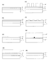
以下に、図1を参照して、本発明による結晶質半導体膜の製造方法の実施形態を説明する。 Hereinafter, an embodiment of a method for producing a crystalline semiconductor film according to the present invention will be described with reference to FIG.
図1(a)に示すように、非晶質半導体膜3を用意する。非晶質半導体膜3は、例えば非晶質ケイ素膜である。まず、ガラス基板1上に厚さ約100nmの酸化ケイ素膜2(例えば、テトラエチルオルソシリケート(Tetraethylorthosilicate:TEOS)膜を堆積し、次いで、SiH4を用いた減圧化学気相成長(Low Pressure Chemical Vapor Deposition:LPCVD)法により、酸化ケイ素膜2上に厚さ70nmの非晶質ケイ素膜3を堆積する。
As shown in FIG. 1A, an
次に、図1(b)に示すように、触媒元素4を非晶質ケイ素膜3に添加する。触媒元素4は、後の熱処理において非晶質ケイ素膜3の結晶化を助長する元素であり、例えば、Niである。Niは例えば抵抗加熱法によって非晶質ケイ素膜3上に蒸着された後、非晶質ケイ素膜3内に拡散される。なお、図1(b)では触媒元素4を膜状に示しているが、実際には、触媒元素4は非晶質ケイ素膜3の表面付近に分散されている。非晶質ケイ素膜3の表面における触媒元素の濃度(表面濃度)は5×10¹⁰atoms/cm2である。
Next, as shown in FIG. 1B, the catalytic element 4 is added to the
その後、非晶質ケイ素膜3を熱処理することにより、非晶質ケイ素膜3を結晶化して、図1(c)に示した結晶質ケイ素膜3’を得る。ここでは、結晶質ケイ素膜3’は多結晶ケイ素膜である。熱処理により、固相結晶成長(Solid phase crystallization:SPC)が行われ、非晶質ケイ素膜3が結晶化される。なお、本明細書において、このように熱処理によって結晶化を行うことを第1結晶化とも称する。上述したように、非晶質ケイ素膜3には触媒元素4が添加されているので、窒素雰囲気の電気炉において非晶質ケイ素膜3を600℃で1時間加熱すると、数μm以上の粒径を有する結晶粒が容易に形成される。ここでは、多結晶ケイ素膜3’の結晶粒は約4μm程度であり、原子間力顕微鏡(Atomic Force Microscope:AFM)で測定したところ、一片が10μmの任意の正方形領域内の平均表面粗さ(Ra値)は1nmであった。
Thereafter, the
次いで、多結晶ケイ素膜3’の表面に凹凸形状を付与する。図1(d)〜図1(f)を参照して多結晶ケイ素膜3’への凹凸形状の付与を説明する。まず、図1(d)に示すように、第1結晶化で得られた多結晶ケイ素膜3’の表面全面にフォトレジストを塗布し、フォトレジスト層5を形成する。フォトレジスト層5の厚さは、例えば、1.0μmである。
Next, an uneven shape is imparted to the surface of the polycrystalline silicon film 3 '. With reference to FIGS. 1 (d) to 1 (f), description will be given of the provision of the uneven shape to the polycrystalline silicon film 3 '. First, as shown in FIG. 1D, a photoresist is applied to the entire surface of the
次いで、図1(e)に示すように、フォトレジスト層5の表面を凹凸形状にしたフォトレジスト層5’を形成する。フォトレジスト層5’は、一般的なエキシマレーザの露光および現像を行うことによって形成される。エキシマレーザの露光は、例えば約1.5μm周期のチェック模様のフォトマスク(図示せず)を通過したArFエキシマレーザを、フォトレジスト層5上でフォトマスクの模様が5分の1に縮小されるように結像することによって行われる。次いで、現像を行うことにより、フォトレジスト層5の露光された部分が除去される。このように形成されたフォトレジスト層5’は約0.3μmの周期的なパターンを有しており、フォトレジスト層5’の開口部分、すなわち、フォトレジスト層5の除去された部分から多結晶ケイ素膜3’が露出している。
Next, as shown in FIG. 1E, a photoresist layer 5 'having an uneven surface is formed. The photoresist layer 5 'is formed by performing general excimer laser exposure and development. In the excimer laser exposure, for example, an ArF excimer laser that has passed a check pattern photomask (not shown) with a period of about 1.5 μm is reduced to 1/5 on the
次いで、多結晶ケイ素膜3’の一部を除去するようにCF4を含むガスを用いてドライエッチングを行った後、フォトレジスト層5’を除去し、図1(f)に示すように、多結晶ケイ素膜3’’を形成する。ドライエッチングによって多結晶ケイ素膜3’の露出された部分が除去されることにより、多結晶ケイ素膜3’’の凹部分が形成される。また、多結晶ケイ素膜3’のうちのフォトレジスト層5’によって覆われていた部分は、多結晶ケイ素膜3’’の凸部分となる。
Next, after performing dry etching using a gas containing CF 4 so as to remove a part of the
ドライエッチングは、例えば、流量800sccmのCF4ガスおよび流量200sccmのO2ガスを導入して圧力が100mTorrになるように調整されたエッチング処理室内で、3kWの高周波電力(Radio Frequency(RF) Power)を30秒間印加することによって行われる。なお、熱処理を行う際に多結晶ケイ素膜3’の表面には酸化膜が形成されているが、ドライエッチングにより、多結晶ケイ素膜3’の一部とともに酸化膜も除去される。ドライエッチング後における多結晶ケイ素膜3’’の表面は、フォトレジスト層5’のパターンに対応する周期的な凹凸形状を有している。ここで、凹凸の周期は0.3μmであり、多結晶ケイ素膜3’’の表面の凹凸の最大高さは50nmであった。また、AFMで測定したところ、一片が10μmの任意の正方形領域内の平均表面粗さ(Ra値)は8nmであった。なお、一般的なレーザアニール法によって半導体膜を結晶化する際に半導体膜にリッジが形成されることがあるが、レーザアニール法ではリッジがランダムに形成されるのに対して、本実施形態では、レーザー照射を行うことなく多結晶ケイ素膜3’’に凹凸形状を付与しており、多結晶ケイ素膜3’’の凹凸形状は周期的または規則的に形成されている。
In dry etching, for example, 3 kW high frequency power (Radio Frequency (RF) Power) is used in an etching process chamber in which CF 4 gas with a flow rate of 800 sccm and O 2 gas with a flow rate of 200 sccm is introduced to adjust the pressure to 100 mTorr. Is applied for 30 seconds. Although an oxide film is formed on the surface of the
次に、多結晶ケイ素膜3’’の表面に形成された酸化膜を除去する。ここで除去される酸化膜は、自然酸化によって形成されたもの、および、フォトレジスト層5’によって覆われていたものである。酸化膜の除去は、例えば、多結晶ケイ素膜3’’の表面に1%のフッ酸溶液を90秒間浸漬させ、スピン乾燥させるウェットエッチングよって行われる。このようなウェットエッチングは、簡便で量産性にも優れている。
Next, the oxide film formed on the surface of the
次に、酸化膜を除去した基板を乾燥させて直ちにチャンバに導入する。チャンバにはレーザビーム照射機構が設けられており、チャンバは、酸素濃度が0.1ppmである1.1気圧の窒素で満たされている。次に、多結晶ケイ素膜3’’にレーザビームを照射する。本明細書において、レーザビームの照射によって結晶性を向上させることを第2結晶化とも称する。図1(g)は、多結晶ケイ素膜3’’に対してレーザビーム6を相対的に走査していることを示す平面図である。レーザビーム6は、多結晶ケイ素膜3’’を部分的に溶融するエネルギー密度で照射される。レーザビーム6が多結晶ケイ素膜3’’を部分的に溶融することにより、結晶は溶融されなかった結晶粒を種結晶として成長し、結果として、粒径の大きな結晶粒を得ることができる。レーザビーム6として、例えば、エネルギー密度340mJ/cm2、パルス幅30nsおよび波長308nmのXeClレーザビームが用いられる。
Next, the substrate from which the oxide film has been removed is dried and immediately introduced into the chamber. The chamber is provided with a laser beam irradiation mechanism, and the chamber is filled with 1.1 atmospheric pressure nitrogen having an oxygen concentration of 0.1 ppm. Next, the
図1(g)に示すように、レーザビーム6は、多結晶ケイ素膜3’’の表面においてエネルギー分布が一様となるように長さ100mm以上の線状に成形されており、ガラス基板1上を短軸方向に20μm/パルスのステップで紙面下方から上方に走査するレーザビーム6を走査することにより、ほぼ全面で充分な結晶性を有する多結晶ケイ素膜3’’’が得られる。なお、ここでいう「線状」とは、厳密な意味で「線」を意味しているのではなく、アスペクト比の大きい長方形または長楕円形を意味する。線状のレーザビームは、例えば、アスペクト比は、2以上好ましくは10〜10000であり、照射面における形状が矩形状であるレーザビーム(矩形状ビーム)を含んでいる。例えば、レーザビーム6は125mm×0.4mmの線状に成形されている。なお、レーザビーム6を線状に成形するのは被照射体に対して充分なアニールを行うためのエネルギー密度を確保するためであり、被照射体に対して充分なアニールを行うことができるのであれば、レーザビーム6の照射面は、線状以外の矩形状であっても、あるいは、数cm角の四角であってもよい。
As shown in FIG. 1G, the laser beam 6 is formed in a linear shape having a length of 100 mm or more so that the energy distribution is uniform on the surface of the
レーザビーム6の照射により、上述したように意図的に設けた凹凸形状の表面を有する多結晶ケイ素膜3’’が溶融すると、表面張力によって表面が平坦になるようにケイ素原子が大きく移動する。ケイ素原子は結晶欠陥を大幅に減少するように移動するため、多結晶ケイ素膜3’’の結晶性が向上する。また、ケイ素原子が移動することにより、多結晶ケイ素膜3’’の表面が平坦化される。したがって、表面が平坦で良好な結晶性を有する多結晶ケイ素膜3’’’が得られる。
When the
図1(h)に示すように、レーザビームの照射によって溶融された後で固化した多結晶ケイ素膜3’’’は平坦な表面を有している。AFMで測定したところ、一片が10μmの任意の正方形領域内の平均表面粗さ(Ra値)は1nmであった。本実施形態では、以上のようにして、結晶性の良い平坦化された多結晶ケイ素膜3’’’を作製することができる。
As shown in FIG. 1 (h), the
本実施形態では、上述したように、レーザビーム6の照射を酸素濃度の低い雰囲気で行っており、これにより、リッジが形成されることを防ぐことができ、平坦化された多結晶ケイ素膜3’’’を得ることができる。また、本実施形態では、凹凸形状を有する多結晶ケイ素膜3’’にレーザビーム6を照射しているため、凸部分を構成するケイ素原子が凹部分に移動し、それにより、レーザビーム6を照射する際の周囲の酸素濃度が低くても、結晶性の向上した多結晶ケイ素膜3’’’を得ることができる。このように、本実施形態では、レーザビーム6の照射により、結晶性の向上だけでなく平坦化を行うことができる。これに対して、酸素濃度の高い雰囲気で行われる一般的なレーザアニール法では、リッジが形成されるため、平坦化のために再度酸化膜除去と酸素濃度の低い雰囲気でのレーザビームの照射が必要となる。また、レーザビームの照射を行っていない平坦な多結晶ケイ素膜に酸素濃度の低い雰囲気でレーザビームを照射しても、ケイ素膜を構成する原子はほとんど移動しないため、結晶欠陥を充分減少させることができず、良好な結晶性を有する多結晶ケイ素膜を得ることはできない。
In the present embodiment, as described above, the irradiation of the laser beam 6 is performed in an atmosphere having a low oxygen concentration, whereby formation of a ridge can be prevented and the planarized
また、本実施形態では、レーザビームの照射は1回のみであるため、特許文献3に開示されている方法と比べて多結晶ケイ素膜3’’’における微小孔の発生を抑制することができ、それにより、この多結晶ケイ素膜3’’’を用いて良好な特性を有する半導体装置を歩留まりよく作製することができる。
Further, in this embodiment, since the laser beam is irradiated only once, generation of micropores in the
なお、上述した説明では、半導体膜としてケイ素膜を用いたが、本発明はこれに限定されない。半導体膜として、ゲルマニウム膜あるいはゲルマニウムとケイ素との混成膜(シリコン・ゲルマニウム膜)を用いてもよい。 In the above description, the silicon film is used as the semiconductor film, but the present invention is not limited to this. As the semiconductor film, a germanium film or a mixed film of germanium and silicon (silicon / germanium film) may be used.
また、上述した説明では、触媒元素はNiであり、非晶質ケイ素膜における触媒元素の表面濃度は5×10¹⁰atoms/cm2であったが、本発明はこれに限定されない。触媒元素は、鉄、コバルト、ニッケル、ゲルマニウム、ルテニウム、ロジウム、パラジウム、オスニウム、イリジウム、白金、銅および金からなる群から選択された少なくとも1種類の元素を含んでいればよい。また、非晶質ケイ素膜における触媒元素の表面濃度は、1×1010atoms/cm2以上1×1012atoms/cm2以下であることが好ましい。表面濃度が1×1010atoms/cm2未満である場合、触媒元素の効果が小さく、結晶化に要する時間が長くなり、製造工程上好ましくない。一方、表面濃度が1×1012atoms/cm2よりも高い場合、触媒元素に起因して結晶粒密度が高くなり、粒径の大きな結晶粒を形成することができず、高いキャリア移動度を得ることができない。 In the above description, the catalytic element is Ni, and the surface concentration of the catalytic element in the amorphous silicon film is 5 × 10 10 atoms / cm 2 , but the present invention is not limited to this. The catalytic element may contain at least one element selected from the group consisting of iron, cobalt, nickel, germanium, ruthenium, rhodium, palladium, osnium, iridium, platinum, copper and gold. The surface concentration of the catalytic element in the amorphous silicon film is preferably 1 × 10 10 atoms / cm 2 or more and 1 × 10 12 atoms / cm 2 or less. When the surface concentration is less than 1 × 10 10 atoms / cm 2 , the effect of the catalytic element is small and the time required for crystallization becomes long, which is not preferable in the manufacturing process. On the other hand, when the surface concentration is higher than 1 × 10 12 atoms / cm 2 , the crystal grain density is increased due to the catalytic element, and a crystal grain having a large grain size cannot be formed, resulting in high carrier mobility. Can't get.
また、上述した説明では、熱処理における加熱温度は600℃であったが、本発明はこれに限定されない。ただし、加熱温度は500℃以上700℃以下であることが好ましい。処理温度が500℃未満の場合、固相結晶成長速度が遅く、製造工程上好ましくない。一方、加熱温度が700℃よりも高い場合、触媒元素に起因して粒径の大きな(例えば、数μm以上)結晶粒が形成されるのに加えて、触媒元素に起因することなく粒径の小さな(例えば、0.2μm以下)結晶粒が形成され、それにより、高いキャリア移動度を得ることができない。また、上述した説明では、加熱時間は1時間であったが、本発明はこれに限定されない。加熱時間は、ガラス基板の変形量やガラス基板からの不純物拡散量、加熱温度等に応じて異なるが、15分以上24時間以下であってもよい。 In the above description, the heating temperature in the heat treatment is 600 ° C., but the present invention is not limited to this. However, the heating temperature is preferably 500 ° C. or higher and 700 ° C. or lower. When the processing temperature is less than 500 ° C., the solid phase crystal growth rate is slow, which is not preferable in the production process. On the other hand, when the heating temperature is higher than 700 ° C., in addition to the formation of crystal grains having a large particle size (for example, several μm or more) due to the catalytic element, Small crystal grains (for example, 0.2 μm or less) are formed, so that high carrier mobility cannot be obtained. In the above description, the heating time is 1 hour, but the present invention is not limited to this. The heating time varies depending on the amount of deformation of the glass substrate, the amount of impurity diffusion from the glass substrate, the heating temperature, etc., but may be 15 minutes or longer and 24 hours or shorter.
また、上述した説明では、凹凸形状の付与された多結晶ケイ素膜のRa値は8nmであったが、本発明はこれに限定されない。ただし、凹凸形状の付与された多結晶ケイ素膜のRa値は2nm以上20nm以下であることが好ましい。より好ましくは多結晶ケイ素膜のRa値は6nm以上9nm以下の範囲である。Ra値が2nm未満の場合は、多結晶ケイ素膜の表面に所定の凹凸形状を付与した効果が少なくなり、充分に良好な結晶性を有する多結晶ケイ素膜が得られなくなる場合がある。一方、Ra値が20nmより大きくなると、次のレーザアニール工程で充分な平坦化を行うことができない場合がある。 In the above description, the Ra value of the polycrystalline silicon film provided with the uneven shape is 8 nm, but the present invention is not limited to this. However, it is preferable that the Ra value of the polycrystalline silicon film provided with the uneven shape is 2 nm or more and 20 nm or less. More preferably, the Ra value of the polycrystalline silicon film is in the range of 6 nm to 9 nm. When the Ra value is less than 2 nm, the effect of imparting a predetermined uneven shape to the surface of the polycrystalline silicon film is reduced, and a polycrystalline silicon film having sufficiently good crystallinity may not be obtained. On the other hand, if the Ra value is greater than 20 nm, sufficient planarization may not be performed in the next laser annealing step.
また、上述した説明では、凹凸形状の付与された多結晶ケイ素膜の表面は0.3μmの周期なチェック模様であったが、本発明はこれに限定されない。多結晶ケイ素膜の表面の凹凸は、凹部分および凸部分がそれぞれレーザビームの走査方向と平行する方向、あるいは直交する方向に伸びるような波状であってもよい。また、多結晶ケイ素膜の表面は0.1μm以上1.5μm以下の周期的な凸凹形状であってもよい。また、上述した説明では、多結晶ケイ素膜の凸凹形状の最大高さは50nmであったが、本発明はこれに限定されない。最大高さは、20nm以上150nm以下であってもよい。 In the above description, the surface of the polycrystalline silicon film provided with the uneven shape has a periodic check pattern of 0.3 μm, but the present invention is not limited to this. The irregularities on the surface of the polycrystalline silicon film may be wavy such that the concave portions and the convex portions extend in a direction parallel to or orthogonal to the scanning direction of the laser beam. Further, the surface of the polycrystalline silicon film may have a periodic uneven shape of 0.1 μm to 1.5 μm. In the above description, the maximum height of the uneven shape of the polycrystalline silicon film is 50 nm, but the present invention is not limited to this. The maximum height may be 20 nm or more and 150 nm or less.
また、上述した説明では、フォトレジスト層の完全露光を行った後にドライエッチングを行い、多結晶ケイ素膜に凹凸形状を付与したが、本発明はこれに限定されない。フォトレジスト層のハーフ露光を行った後にドライエッチングを行い、多結晶ケイ素膜に凹凸形状を付与してもよい。 In the above description, the photoresist layer is completely exposed and then dry etching is performed to give the polycrystalline silicon film an uneven shape. However, the present invention is not limited to this. After the half exposure of the photoresist layer, dry etching may be performed to give the polycrystalline silicon film an uneven shape.
また、上述した説明では、チャンバ内の酸素濃度は0.1ppmであり、気体は窒素であったが、本発明はこれに限定されない。ただし、チャンバ内の酸素濃度は10ppm以下であることが好ましい。酸素濃度が10ppmよりも高いと、レーザビームの照射により、多結晶ケイ素膜の表面にリッジが形成され、充分に平坦化を行うことができないからである。また、不活性気体は窒素または希ガスの少なくとも一種類の元素を含んでいればよい。不活性気体は、製造コストを下げるために上述したように窒素を用いることが好ましいが、希ガスを用いても同様の効果を得ることができる。 In the above description, the oxygen concentration in the chamber is 0.1 ppm and the gas is nitrogen. However, the present invention is not limited to this. However, the oxygen concentration in the chamber is preferably 10 ppm or less. This is because, when the oxygen concentration is higher than 10 ppm, a ridge is formed on the surface of the polycrystalline silicon film by laser beam irradiation, and sufficient planarization cannot be performed. Moreover, the inert gas should just contain at least 1 type of element of nitrogen or a noble gas. As described above, nitrogen is preferably used as the inert gas in order to reduce the manufacturing cost, but the same effect can be obtained even when a rare gas is used.
また、上述した説明では、レーザビームの波長は308nmであったが、本発明はこれに限定されない。レーザビームの波長は126nmから370nmの範囲であってもよい。また、上述した説明では、パルス発振エキシマレーザビームの一例としてXeClレーザビームを用いたが、本発明はこれに限定されない。他のパルス発振エキシマレーザビーム、例えば、KrF、XeF、ArClまたはKrClレーザビームを用いてもよい。 In the above description, the wavelength of the laser beam is 308 nm, but the present invention is not limited to this. The wavelength of the laser beam may be in the range of 126 nm to 370 nm. In the above description, the XeCl laser beam is used as an example of the pulsed excimer laser beam, but the present invention is not limited to this. Other pulsed excimer laser beams, such as KrF, XeF, ArCl or KrCl laser beams may be used.
また、上述した説明では、多結晶ケイ素膜3’’を部分的に溶融させるレーザビームのエネルギー密度として340mJ/cm2を例示したが、本発明はこれに限定されない。ただし、本発明者の研究結果によれば、レーザビームのエネルギー密度が350mJ/cm2以上であると、エネルギー密度が高過ぎて多結晶ケイ素膜3’’が完全に溶融し、微結晶となる領域が発生する。また、レーザビームのエネルギー密度が330mJ/cm2未満であると、X線回折分析の結果から、レーザビームのエネルギー密度が330mJ/cm2以上である場合と比べて結晶性が低下していることがわかる。したがって、上述したように、エネルギー密度が340mJ/cm2であると、多結晶ケイ素膜を部分的に溶融させることができ、ほぼ全面が充分な結晶性を有する多結晶ケイ素膜を得ることができる。また、第2結晶化においてレーザアニール法を用いる場合、ケイ素膜の表面で線状に成形されたパルス発振エキシマレーザビームを短軸方向にステップ走査することにより、大面積のケイ素膜を効率よく簡便に処理することができる。
In the above description, 340 mJ / cm 2 is exemplified as the energy density of the laser beam for partially melting the
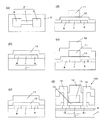
また、以上の方法に従って製造された多結晶ケイ素膜を活性層に使用したTFTは高いキャリア移動度を示す。以下に、図2を参照して、多結晶ケイ素膜3’’’を活性層として用いたnチャネル型電界効果薄膜トランジスタ(以下、「nチャネル型TFT」という。)100の製造方法を説明する。
A TFT using a polycrystalline silicon film manufactured according to the above method as an active layer exhibits high carrier mobility. A method for manufacturing an n-channel field effect thin film transistor (hereinafter referred to as “n-channel TFT”) 100 using the
図2(a)に示すように、まず、ガラス基板1(図1(a)参照、図2(a)には図示せず)上に配置された酸化ケイ素膜2の上に作製された多結晶ケイ素膜3’’’を、チャネル領域7、ソース領域8およびドレイン領域9に対応する形状にパタ−ニングする。図2(b)に示すように、多結晶ケイ素膜3’’’を覆うように、常圧化学気相成長Atmospheric Pressure Chemical Vapor Deposition:APCVD)法により、厚さ100nm程度の酸化膜からなるゲート絶縁膜10を形成する。
As shown in FIG. 2A, first, a multi-layer formed on a
次に、図2(c)に示すように、ゲート絶縁膜10上に、導電膜11’として厚さ300nm程度のアルミニウム膜を形成し、図2(d)に示すように、アルミニウム膜11’を所定形状にパターニングしてゲート電極11を形成する。このゲート電極11をマスクとして、ソース領域8およびドレイン領域9となる領域にリンイオンを注入し、ゲート電極11直下のチャネル領域7の両側にソ−ス領域8およびドレイン領域9を形成する。
Next, as shown in FIG. 2C, an aluminum film having a thickness of about 300 nm is formed as the
その後、図2(e)に示すように、APCVD法によって、ガラス基板1上の全面にゲート電極11を覆うように厚さ500nmの酸化膜を堆積して層間絶縁膜12を形成する。次いで、図2(f)に示すように、ソ−ス領域8およびドレイン領域9上のゲート絶縁膜10および層間絶縁膜12にコンタクトホ−ル部を形成し、スパッタリング法によって電極材料をコンタクトホ−ル部に堆積させ、コンタクトホール部を介して電極材料とソース領域8およびドレイン領域9との間にオ−ミック接触を実現させる。この電極材料を所定形状にパターニングすることにより、引き出し電極13が形成される。以上のようにして、nチャネル型TFT100が作製される。このようにして作製されたnチャネル型TFT100のキャリア移動度を測定したところ、高いキャリア移動度(350cm2 /V・s)を示した。また、多結晶領域だけでなく、第2結晶化におけるレーザビームの照射により微結晶が形成された領域、および、多結晶と微結晶との境界を活性層に含むトランジスタでも同様のキャリア移動度を示した。なお、参考のために、凹凸形状を付与することなくレーザビームの照射を1回行って多結晶ケイ素膜を形成し、その多結晶ケイ素膜を用いて作製したnチャネル型TFTのキャリア移動度を測定したところ、キャリア移動度は80cm2 /V・sであった。
Thereafter, as shown in FIG. 2E, an
なお、上述した説明では、TFTの例示としてnチャネル型TFT100を説明したが本発明はこれに限定されない。多結晶ケイ素膜3’’’を用いてpチャネル型TFTを作製してもよい。また、nおよび/またはpチャネル型TFTをスイッチング素子として用いた半導体装置をさらに作製してもよい。
In the above description, the n-
本発明によれば、微小孔の発生を抑制するとともに良好な結晶性を有する平坦化された結晶質半導体膜を製造することができ、この結晶質半導体膜を用いて、キャリア移動度の高い電界効果薄膜トランジスタに好適に作製することができる。また、このような電界効果薄膜トランジスタを有する半導体装置は、表示媒体として液晶などを利用したアクティブマトリクス方式の表示装置などに好適に用いられる。特に、表示媒体として液晶などを用いたアクティブマトリクス方式の表示装置において、このようなキャリア移動度の大きい半導体装置をスイッチング素子や駆動回路などに用いることにより、表示装置の高性能化および高画質化を実現することができる。 According to the present invention, it is possible to manufacture a planarized crystalline semiconductor film that suppresses the generation of micropores and has good crystallinity, and an electric field with high carrier mobility can be produced using this crystalline semiconductor film. It can produce suitably for an effect thin-film transistor. Further, a semiconductor device having such a field effect thin film transistor is preferably used for an active matrix type display device using liquid crystal as a display medium. In particular, in an active matrix display device using liquid crystal as a display medium, a semiconductor device having such a high carrier mobility is used for a switching element, a drive circuit, etc., thereby improving the performance and image quality of the display device. Can be realized.
1 基板
2 酸化ケイ素膜
3 非晶質半導体膜
3’、3’’、3’’’ 結晶質半導体膜
4 触媒元素
5、5’ フォトレジスト層
6 レーザビーム
7 チャネル領域
8 ソース領域
9 ドレイン領域
10 ゲート絶縁膜
11 ゲート電極
11’ 導電膜
12 層間絶縁膜
13 引き出し電極
100 nチャネル型TFT
DESCRIPTION OF
Claims (16)
前記非晶質半導体膜の結晶化を助長する触媒元素を前記非晶質半導体膜に添加する工程と、
前記触媒元素の添加された非晶質半導体膜に熱処理を行うことにより、結晶質半導体膜を得る工程と、
前記結晶質半導体膜の表面に所定の凹凸形状を付与する工程と、
前記結晶質半導体膜の表面に所定の凹凸形状を付与した後、前記結晶質半導体膜の表面に形成された酸化膜を除去する工程と、
前記酸化膜を除去した後、前記結晶質半導体膜にレーザビームを照射する工程と
を包含する、結晶質半導体膜の製造方法。 Preparing an amorphous semiconductor film;
Adding a catalytic element for promoting crystallization of the amorphous semiconductor film to the amorphous semiconductor film;
A step of obtaining a crystalline semiconductor film by performing a heat treatment on the amorphous semiconductor film to which the catalytic element is added;
Providing a predetermined uneven shape on the surface of the crystalline semiconductor film;
A step of removing an oxide film formed on the surface of the crystalline semiconductor film after providing a predetermined uneven shape on the surface of the crystalline semiconductor film;
And a step of irradiating the crystalline semiconductor film with a laser beam after removing the oxide film.
前記結晶質半導体膜の表面に凹凸形状を有するフォトレジスト層を形成する工程と、
ドライエッチングにより、前記フォトレジスト層および前記結晶質半導体膜の一部を除去する工程と
を含む、請求項1から5のいずれかに記載の結晶質半導体膜の製造方法。 The step of providing a predetermined uneven shape on the surface of the crystalline semiconductor film,
Forming a photoresist layer having a concavo-convex shape on the surface of the crystalline semiconductor film;
The method for producing a crystalline semiconductor film according to claim 1, further comprising a step of removing part of the photoresist layer and the crystalline semiconductor film by dry etching.
Priority Applications (1)
| Application Number | Priority Date | Filing Date | Title |
|---|---|---|---|
| JP2006145233A JP2007317841A (en) | 2006-05-25 | 2006-05-25 | Method for manufacturing crystalline semiconductor film |
Applications Claiming Priority (1)
| Application Number | Priority Date | Filing Date | Title |
|---|---|---|---|
| JP2006145233A JP2007317841A (en) | 2006-05-25 | 2006-05-25 | Method for manufacturing crystalline semiconductor film |
Publications (1)
| Publication Number | Publication Date |
|---|---|
| JP2007317841A true JP2007317841A (en) | 2007-12-06 |
Family
ID=38851450
Family Applications (1)
| Application Number | Title | Priority Date | Filing Date |
|---|---|---|---|
| JP2006145233A Pending JP2007317841A (en) | 2006-05-25 | 2006-05-25 | Method for manufacturing crystalline semiconductor film |
Country Status (1)
| Country | Link |
|---|---|
| JP (1) | JP2007317841A (en) |
Cited By (1)
| Publication number | Priority date | Publication date | Assignee | Title |
|---|---|---|---|---|
| KR20120139570A (en) * | 2011-06-16 | 2012-12-27 | 가부시키가이샤 한도오따이 에네루기 켄큐쇼 | Semiconductor device and method for manufacturing the same |
-
2006
- 2006-05-25 JP JP2006145233A patent/JP2007317841A/en active Pending
Cited By (2)
| Publication number | Priority date | Publication date | Assignee | Title |
|---|---|---|---|---|
| KR20120139570A (en) * | 2011-06-16 | 2012-12-27 | 가부시키가이샤 한도오따이 에네루기 켄큐쇼 | Semiconductor device and method for manufacturing the same |
| KR102055538B1 (en) | 2011-06-16 | 2019-12-13 | 가부시키가이샤 한도오따이 에네루기 켄큐쇼 | Semiconductor device and method for manufacturing the same |
Similar Documents
| Publication | Publication Date | Title |
|---|---|---|
| JP3942651B2 (en) | Method for manufacturing semiconductor device | |
| US6919237B2 (en) | Process for fabricating thin film transistors | |
| US5854096A (en) | Process for fabricating semiconductor device | |
| JP4291539B2 (en) | Semiconductor device and manufacturing method thereof | |
| JP3658213B2 (en) | Manufacturing method of semiconductor device | |
| KR100279106B1 (en) | Manufacturing method of semiconductor device | |
| JP3389022B2 (en) | Semiconductor device | |
| JPH1140501A (en) | Semiconductor device manufacturing method and semiconductor device | |
| CN1097298C (en) | Method of making crystal silicon semiconductor and thin film transistor | |
| JP3522441B2 (en) | Semiconductor device | |
| JP3432187B2 (en) | Method for manufacturing semiconductor device | |
| WO2011078005A1 (en) | Semiconductor device and process for production thereof, and display device | |
| JP3981532B2 (en) | Manufacturing method of semiconductor device | |
| KR100761346B1 (en) | Method for producing crystalline silicon | |
| JP3630593B2 (en) | Semiconductor device, method for manufacturing semiconductor device, and liquid crystal display device | |
| JP4289816B2 (en) | Semiconductor device and manufacturing method thereof | |
| JP2009246235A (en) | Method of manufacturing semiconductor substrate, semiconductor substrate, and display device | |
| JP2007317841A (en) | Method for manufacturing crystalline semiconductor film | |
| KR20030015617A (en) | Method of manufacturing a crystalloid silicone | |
| JP3545104B2 (en) | Manufacturing method of thin film semiconductor | |
| KR100413473B1 (en) | Crystallization method for amorphous silicon using hydrogen plasma and electric field | |
| JP3857085B2 (en) | Thin film transistor and manufacturing method thereof | |
| KR100860008B1 (en) | Flat panel display device and its manufacturing method using directional crystallization method, semiconductor device and manufacturing method thereof | |
| JP3999923B2 (en) | Semiconductor device and manufacturing method thereof | |
| JP3842083B2 (en) | Thin film transistor, manufacturing method thereof, and display device |