EP0459836B1 - Method for fabricating thin-film transistors - Google Patents
Method for fabricating thin-film transistors Download PDFInfo
- Publication number
- EP0459836B1 EP0459836B1 EP91305013A EP91305013A EP0459836B1 EP 0459836 B1 EP0459836 B1 EP 0459836B1 EP 91305013 A EP91305013 A EP 91305013A EP 91305013 A EP91305013 A EP 91305013A EP 0459836 B1 EP0459836 B1 EP 0459836B1
- Authority
- EP
- European Patent Office
- Prior art keywords
- source
- drain
- layers
- semiconductor layer
- single crystal
- Prior art date
- Legal status (The legal status is an assumption and is not a legal conclusion. Google has not performed a legal analysis and makes no representation as to the accuracy of the status listed.)
- Expired - Lifetime
Links
- 238000000034 method Methods 0.000 title claims description 43
- 239000010409 thin film Substances 0.000 title claims description 7
- 239000010408 film Substances 0.000 claims description 50
- 239000004065 semiconductor Substances 0.000 claims description 49
- 239000013078 crystal Substances 0.000 claims description 15
- 239000000758 substrate Substances 0.000 claims description 13
- 239000000463 material Substances 0.000 claims description 10
- 230000001678 irradiating effect Effects 0.000 claims description 6
- VYPSYNLAJGMNEJ-UHFFFAOYSA-N Silicium dioxide Chemical compound O=[Si]=O VYPSYNLAJGMNEJ-UHFFFAOYSA-N 0.000 claims description 5
- 229910052814 silicon oxide Inorganic materials 0.000 claims description 5
- 229910052581 Si3N4 Inorganic materials 0.000 claims description 4
- 230000003213 activating effect Effects 0.000 claims description 4
- 238000004519 manufacturing process Methods 0.000 claims description 4
- HQVNEWCFYHHQES-UHFFFAOYSA-N silicon nitride Chemical compound N12[Si]34N5[Si]62N3[Si]51N64 HQVNEWCFYHHQES-UHFFFAOYSA-N 0.000 claims description 4
- 230000015572 biosynthetic process Effects 0.000 claims description 3
- 238000005229 chemical vapour deposition Methods 0.000 claims description 2
- 230000000873 masking effect Effects 0.000 claims description 2
- 238000000059 patterning Methods 0.000 claims description 2
- 230000008569 process Effects 0.000 description 26
- 238000000151 deposition Methods 0.000 description 7
- 239000012535 impurity Substances 0.000 description 7
- 230000008021 deposition Effects 0.000 description 6
- 230000015556 catabolic process Effects 0.000 description 5
- 238000006731 degradation reaction Methods 0.000 description 5
- OAICVXFJPJFONN-UHFFFAOYSA-N Phosphorus Chemical compound [P] OAICVXFJPJFONN-UHFFFAOYSA-N 0.000 description 4
- 230000004913 activation Effects 0.000 description 4
- 238000005530 etching Methods 0.000 description 4
- 239000007789 gas Substances 0.000 description 4
- 229910021421 monocrystalline silicon Inorganic materials 0.000 description 4
- 229910052698 phosphorus Inorganic materials 0.000 description 4
- 239000011574 phosphorus Substances 0.000 description 4
- 230000001681 protective effect Effects 0.000 description 4
- 230000004044 response Effects 0.000 description 4
- 238000011282 treatment Methods 0.000 description 4
- 238000006243 chemical reaction Methods 0.000 description 3
- 238000005468 ion implantation Methods 0.000 description 3
- 229910052782 aluminium Inorganic materials 0.000 description 2
- XAGFODPZIPBFFR-UHFFFAOYSA-N aluminium Chemical compound [Al] XAGFODPZIPBFFR-UHFFFAOYSA-N 0.000 description 2
- 229910021417 amorphous silicon Inorganic materials 0.000 description 2
- 238000000137 annealing Methods 0.000 description 2
- 238000000429 assembly Methods 0.000 description 2
- 230000000712 assembly Effects 0.000 description 2
- 230000008901 benefit Effects 0.000 description 2
- 238000002425 crystallisation Methods 0.000 description 2
- 230000008025 crystallization Effects 0.000 description 2
- 238000005516 engineering process Methods 0.000 description 2
- 230000002349 favourable effect Effects 0.000 description 2
- 230000005669 field effect Effects 0.000 description 2
- 238000005224 laser annealing Methods 0.000 description 2
- 239000004973 liquid crystal related substance Substances 0.000 description 2
- 238000000206 photolithography Methods 0.000 description 2
- 239000005361 soda-lime glass Substances 0.000 description 2
- 238000004544 sputter deposition Methods 0.000 description 2
- UFHFLCQGNIYNRP-UHFFFAOYSA-N Hydrogen Chemical compound [H][H] UFHFLCQGNIYNRP-UHFFFAOYSA-N 0.000 description 1
- BLRPTPMANUNPDV-UHFFFAOYSA-N Silane Chemical compound [SiH4] BLRPTPMANUNPDV-UHFFFAOYSA-N 0.000 description 1
- XUIMIQQOPSSXEZ-UHFFFAOYSA-N Silicon Chemical compound [Si] XUIMIQQOPSSXEZ-UHFFFAOYSA-N 0.000 description 1
- 239000005388 borosilicate glass Substances 0.000 description 1
- 230000008859 change Effects 0.000 description 1
- 230000006378 damage Effects 0.000 description 1
- 230000000593 degrading effect Effects 0.000 description 1
- 238000010586 diagram Methods 0.000 description 1
- 239000011521 glass Substances 0.000 description 1
- 229910052736 halogen Inorganic materials 0.000 description 1
- 150000002367 halogens Chemical class 0.000 description 1
- 238000010438 heat treatment Methods 0.000 description 1
- 229910052739 hydrogen Inorganic materials 0.000 description 1
- 239000001257 hydrogen Substances 0.000 description 1
- 230000007774 longterm Effects 0.000 description 1
- 229910052751 metal Inorganic materials 0.000 description 1
- 239000002184 metal Substances 0.000 description 1
- 229910044991 metal oxide Inorganic materials 0.000 description 1
- 150000004706 metal oxides Chemical class 0.000 description 1
- 230000004048 modification Effects 0.000 description 1
- 238000012986 modification Methods 0.000 description 1
- 230000003071 parasitic effect Effects 0.000 description 1
- 230000000149 penetrating effect Effects 0.000 description 1
- 238000009832 plasma treatment Methods 0.000 description 1
- 229910021420 polycrystalline silicon Inorganic materials 0.000 description 1
- 229910052710 silicon Inorganic materials 0.000 description 1
- 239000010703 silicon Substances 0.000 description 1
- 238000000859 sublimation Methods 0.000 description 1
- 230000008022 sublimation Effects 0.000 description 1
- 239000000126 substance Substances 0.000 description 1
- 230000003685 thermal hair damage Effects 0.000 description 1
- 238000007669 thermal treatment Methods 0.000 description 1
Images

Classifications
-
- H—ELECTRICITY
- H01—ELECTRIC ELEMENTS
- H01L—SEMICONDUCTOR DEVICES NOT COVERED BY CLASS H10
- H01L21/00—Processes or apparatus adapted for the manufacture or treatment of semiconductor or solid state devices or of parts thereof
- H01L21/02—Manufacture or treatment of semiconductor devices or of parts thereof
- H01L21/02104—Forming layers
- H01L21/02365—Forming inorganic semiconducting materials on a substrate
- H01L21/02656—Special treatments
- H01L21/02664—Aftertreatments
- H01L21/02667—Crystallisation or recrystallisation of non-monocrystalline semiconductor materials, e.g. regrowth
-
- H—ELECTRICITY
- H01—ELECTRIC ELEMENTS
- H01L—SEMICONDUCTOR DEVICES NOT COVERED BY CLASS H10
- H01L21/00—Processes or apparatus adapted for the manufacture or treatment of semiconductor or solid state devices or of parts thereof
- H01L21/02—Manufacture or treatment of semiconductor devices or of parts thereof
- H01L21/02104—Forming layers
- H01L21/02365—Forming inorganic semiconducting materials on a substrate
- H01L21/02367—Substrates
- H01L21/0237—Materials
- H01L21/02422—Non-crystalline insulating materials, e.g. glass, polymers
-
- H—ELECTRICITY
- H01—ELECTRIC ELEMENTS
- H01L—SEMICONDUCTOR DEVICES NOT COVERED BY CLASS H10
- H01L21/00—Processes or apparatus adapted for the manufacture or treatment of semiconductor or solid state devices or of parts thereof
- H01L21/02—Manufacture or treatment of semiconductor devices or of parts thereof
- H01L21/02104—Forming layers
- H01L21/02365—Forming inorganic semiconducting materials on a substrate
- H01L21/02436—Intermediate layers between substrates and deposited layers
- H01L21/02439—Materials
- H01L21/02441—Group 14 semiconducting materials
- H01L21/0245—Silicon, silicon germanium, germanium
-
- H—ELECTRICITY
- H01—ELECTRIC ELEMENTS
- H01L—SEMICONDUCTOR DEVICES NOT COVERED BY CLASS H10
- H01L21/00—Processes or apparatus adapted for the manufacture or treatment of semiconductor or solid state devices or of parts thereof
- H01L21/02—Manufacture or treatment of semiconductor devices or of parts thereof
- H01L21/02104—Forming layers
- H01L21/02365—Forming inorganic semiconducting materials on a substrate
- H01L21/02436—Intermediate layers between substrates and deposited layers
- H01L21/02439—Materials
- H01L21/02488—Insulating materials
-
- H—ELECTRICITY
- H01—ELECTRIC ELEMENTS
- H01L—SEMICONDUCTOR DEVICES NOT COVERED BY CLASS H10
- H01L21/00—Processes or apparatus adapted for the manufacture or treatment of semiconductor or solid state devices or of parts thereof
- H01L21/02—Manufacture or treatment of semiconductor devices or of parts thereof
- H01L21/02104—Forming layers
- H01L21/02365—Forming inorganic semiconducting materials on a substrate
- H01L21/02436—Intermediate layers between substrates and deposited layers
- H01L21/02494—Structure
- H01L21/02496—Layer structure
- H01L21/02502—Layer structure consisting of two layers
-
- H—ELECTRICITY
- H01—ELECTRIC ELEMENTS
- H01L—SEMICONDUCTOR DEVICES NOT COVERED BY CLASS H10
- H01L21/00—Processes or apparatus adapted for the manufacture or treatment of semiconductor or solid state devices or of parts thereof
- H01L21/02—Manufacture or treatment of semiconductor devices or of parts thereof
- H01L21/02104—Forming layers
- H01L21/02365—Forming inorganic semiconducting materials on a substrate
- H01L21/02518—Deposited layers
- H01L21/02521—Materials
- H01L21/02524—Group 14 semiconducting materials
- H01L21/02532—Silicon, silicon germanium, germanium
-
- H—ELECTRICITY
- H01—ELECTRIC ELEMENTS
- H01L—SEMICONDUCTOR DEVICES NOT COVERED BY CLASS H10
- H01L21/00—Processes or apparatus adapted for the manufacture or treatment of semiconductor or solid state devices or of parts thereof
- H01L21/02—Manufacture or treatment of semiconductor devices or of parts thereof
- H01L21/02104—Forming layers
- H01L21/02365—Forming inorganic semiconducting materials on a substrate
- H01L21/02518—Deposited layers
- H01L21/0257—Doping during depositing
- H01L21/02573—Conductivity type
- H01L21/02576—N-type
-
- H—ELECTRICITY
- H01—ELECTRIC ELEMENTS
- H01L—SEMICONDUCTOR DEVICES NOT COVERED BY CLASS H10
- H01L21/00—Processes or apparatus adapted for the manufacture or treatment of semiconductor or solid state devices or of parts thereof
- H01L21/02—Manufacture or treatment of semiconductor devices or of parts thereof
- H01L21/02104—Forming layers
- H01L21/02365—Forming inorganic semiconducting materials on a substrate
- H01L21/02612—Formation types
- H01L21/02617—Deposition types
- H01L21/0262—Reduction or decomposition of gaseous compounds, e.g. CVD
-
- H—ELECTRICITY
- H01—ELECTRIC ELEMENTS
- H01L—SEMICONDUCTOR DEVICES NOT COVERED BY CLASS H10
- H01L21/00—Processes or apparatus adapted for the manufacture or treatment of semiconductor or solid state devices or of parts thereof
- H01L21/02—Manufacture or treatment of semiconductor devices or of parts thereof
- H01L21/02104—Forming layers
- H01L21/02365—Forming inorganic semiconducting materials on a substrate
- H01L21/02612—Formation types
- H01L21/02617—Deposition types
- H01L21/02631—Physical deposition at reduced pressure, e.g. MBE, sputtering, evaporation
-
- H—ELECTRICITY
- H01—ELECTRIC ELEMENTS
- H01L—SEMICONDUCTOR DEVICES NOT COVERED BY CLASS H10
- H01L21/00—Processes or apparatus adapted for the manufacture or treatment of semiconductor or solid state devices or of parts thereof
- H01L21/02—Manufacture or treatment of semiconductor devices or of parts thereof
- H01L21/02104—Forming layers
- H01L21/02365—Forming inorganic semiconducting materials on a substrate
- H01L21/02656—Special treatments
- H01L21/02664—Aftertreatments
- H01L21/02667—Crystallisation or recrystallisation of non-monocrystalline semiconductor materials, e.g. regrowth
- H01L21/02675—Crystallisation or recrystallisation of non-monocrystalline semiconductor materials, e.g. regrowth using laser beams
- H01L21/02686—Pulsed laser beam
-
- H—ELECTRICITY
- H01—ELECTRIC ELEMENTS
- H01L—SEMICONDUCTOR DEVICES NOT COVERED BY CLASS H10
- H01L21/00—Processes or apparatus adapted for the manufacture or treatment of semiconductor or solid state devices or of parts thereof
- H01L21/02—Manufacture or treatment of semiconductor devices or of parts thereof
- H01L21/04—Manufacture or treatment of semiconductor devices or of parts thereof the devices having potential barriers, e.g. a PN junction, depletion layer or carrier concentration layer
- H01L21/18—Manufacture or treatment of semiconductor devices or of parts thereof the devices having potential barriers, e.g. a PN junction, depletion layer or carrier concentration layer the devices having semiconductor bodies comprising elements of Group IV of the Periodic Table or AIIIBV compounds with or without impurities, e.g. doping materials
- H01L21/26—Bombardment with radiation
- H01L21/263—Bombardment with radiation with high-energy radiation
- H01L21/268—Bombardment with radiation with high-energy radiation using electromagnetic radiation, e.g. laser radiation
-
- H—ELECTRICITY
- H01—ELECTRIC ELEMENTS
- H01L—SEMICONDUCTOR DEVICES NOT COVERED BY CLASS H10
- H01L29/00—Semiconductor devices specially adapted for rectifying, amplifying, oscillating or switching and having potential barriers; Capacitors or resistors having potential barriers, e.g. a PN-junction depletion layer or carrier concentration layer; Details of semiconductor bodies or of electrodes thereof ; Multistep manufacturing processes therefor
- H01L29/66—Types of semiconductor device ; Multistep manufacturing processes therefor
- H01L29/66007—Multistep manufacturing processes
- H01L29/66075—Multistep manufacturing processes of devices having semiconductor bodies comprising group 14 or group 13/15 materials
- H01L29/66227—Multistep manufacturing processes of devices having semiconductor bodies comprising group 14 or group 13/15 materials the devices being controllable only by the electric current supplied or the electric potential applied, to an electrode which does not carry the current to be rectified, amplified or switched, e.g. three-terminal devices
- H01L29/66409—Unipolar field-effect transistors
- H01L29/66477—Unipolar field-effect transistors with an insulated gate, i.e. MISFET
- H01L29/66742—Thin film unipolar transistors
- H01L29/6675—Amorphous silicon or polysilicon transistors
- H01L29/66757—Lateral single gate single channel transistors with non-inverted structure, i.e. the channel layer is formed before the gate
Definitions
- the present invention relates to a method for fabricating thin-film transistors (referred to hereinafter as TFTs).
- TFTs Thin-film transistors made with non-single crystal semiconductor materials produced by chemical vapor desposition (referred to hereinafter as CVD) processes or the like have recently become of great interest.
- CVD chemical vapor desposition
- the process can advantageously be carried out at a temperature as low as about 500°C or even less.
- the process becomes economical, since it allows the use of low-cost soda-lime glass, borosilicate glass, and the like as the substrate.
- TFTs are typically field effect transistors which function in a manner similar to so-called MOSFETs (Metal Oxide Silicon Field-Effect Transistors).
- MOSFETs Metal Oxide Silicon Field-Effect Transistors
- TFTs can be deposited at low temperature, and moreover, the maximum area thereof is limited only by the dimensions of the deposition apparatus. Thus, TFTs can be freely and easily scaled up with respect to their area, and this is a great advantage.
- TFTs are, therefore, promising for use as switching devices for active matrix-structured liquid crystal displays consisting of a large number of pixels (picture elements), as well as for one- or two-dimensional image sensors and the like.
- TFTs may be subjected to fine patterning using the well-established technology of photolithography, and thus they may be integrated in the same manner as, for example, ICs.
- FIG. 2 A typical structure of conventional TFTs is schematically shown in Fig. 2 of the accompanying drawings.
- a typical thin film transistor comprises an insulating glass substrate 20, a thin film semiconductor 21 consisting of non-single crystal semiconductor material, a source region 22, a drain region 23, a source contact 24, a drain contact 25, a gate insulating film 26, and a gate contact 27.
- the current between the source 22 and the drain 23 can be controlled by applying a voltage to the gate contact 27.
- the non-single crystal semiconductor layer used in TFTs comprise numerous grain boundaries and the like, and these have greatly reduced the carrier mobility as compared with that of single crystal semiconductors.
- the long delay in response ascribed to the low carrier mobility has been a great problem in non-single crystal semiconductor TFTs.
- TFTs using amorphous silicon (referred to hereinafter as a-Si) semiconductors were not practically feasible, since the mobility thereof was so low as in the range of about 0.1 to 1 cm 2 .V -1 .sec -1 .
- the electric current at the channel portion is subject to the materials of which the source and the drain assemblies are made.
- the source and the drain assemblies are often made polycrystalline, or some treatment is applied thereto to assure good electric contact with the channel portion.
- a thin film of polycrystalline silicon may be deposited by CVD at the source and the drain areas, but the CVD process requires the process to be carried out at a temperature of 500°C or higher.
- a treatment may be carried out to assure good contact between the channel portion and the source and the drain. The treatment comprises, after forming semiconductor layers as the drain and the source, introducing therein an n-type or a p-type impurity by ion-implantation, and then heat-treating the drain and the source at a temperature in a range of from 500 to 800°C.
- EP-A-0 171 509 discloses a process to improve the crystallinity of thin semiconductor films by an irradiation step.
- EP-A-0 301 463 discloses a conventional TFT obtained by irradiation annealing steps.
- Ion implantation is used for obtaining good electric contacts between the channel and the drain and source regions.
- it is extremely difficult to carry out uniform doping of impurities over a large area by ion implantation. This remains a great hindrance to the future development of large-area liquid-crystal displays and the like.
- the present invention provides a process according to claim 1 for fabricating TFTs at low temperature, such process comprising crystallizing the channel portion of a TFT, for example by subjecting it to irradiation with an excimer laser, and modifying the electric properties of the source and drain regions of the TFT, for example by subjecting them to irradiation with an excimer laser, independently of the crystallizing of the channel portion.
- the invention thus provides a two-step laser annealing process for TFTs which is carried out at low temperature.
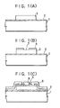
- Fig. 1 schematically illustrates a process for fabricating a planar-type TFT according to an exemplary embodiment of the present invention.
- a soda-lime glass substrate 1 On the surface of a soda-lime glass substrate 1 there was deposited a 300 nm thick silicon oxide film serving as a base protective film 2, the film 2 being deposited by a well known sputtering method.
- the film deposition was carried out under the following conditions: Sputter gas 100% O 2 Reaction pressure 0.5 Pa RF power 400 W Temperature of the substrate 150°C Rate of film deposition 5 nm/min.
- the film 3 was annealed by irradiation with excimer laser energy so as to crystallize the film 3 into a polycrystal.
- the conditions of the annealing process were as follows: Laser energy density 200 mJ/cm 2 Pulse repetition 50 shots.
- n-type non-single crystal silicon film doped with phosphorus such film serving as a low-resistance non-single crystal semiconductor layer.
- the deposition of this film was carried out by plasma chemical vapor deposition under the following conditions: Gas materials SiH 4 + PH 3 + H 2 Reaction pressure 0.05 Torr Temperature of the substrate 300°C RF power (13.56 MHz) 200 W Film thickness 50 nm.
- a microcrystalline film with a low electric resistance may be deposited as the n-type non-single crystal silicon film, by incorporating a large amount of H 2 gas into the gas materials at elevated RF power.
- the n-type non-single crystal semiconductor material of the source and the drain regions 4 was activated by irradiating the same with an excimer laser beam under the following conditions: Laser energy density 100 mJ/cm 2 Pulse repetition 50 shots.
- the channel portion 7 was then activated by plasma treatment in hydrogen under the following conditions: Temperature of the substrate 250°C RF power 100 W Duration of the treatment 60 minutes.
- the formation of the gate oxide film was carried out using the same materials and method as those used in the deposition of the base protective film 2.
- the etching of the contact holes was carried out by a method well known in the art.
- the conductivity of the source and drain n-type non-single crystal semiconductor material 4 changes as a function of the energy density of the irradiating excimer laser beam in the manner shown in Fig. 3.
- the conductivity of the semiconductor 4 increases with increasing energy density up to 150 mJ/cm 2 .
- the conductivity can be seen to decrease with further increase of the energy density since the N + layer surfaces of the source and drain are damaged by high energy laser irradiation. With still further increase of the energy density, the source and drain semiconductors 4 would sublime.
- the laser irradiation should be effected at an energy density preferably of 150 mJ/cm 2 or less, and more preferably in the range of from 100 mJ/cm 2 to 150 mJ/cm 2 .
- an energy density preferably of 150 mJ/cm 2 or less, and more preferably in the range of from 100 mJ/cm 2 to 150 mJ/cm 2 .
- the channel portion Since the channel portion was well crystallized by the laser annealing of the I-type semiconductor film 3, the channel portion would be degraded by the laser irradiation of the source and drain semiconductors 4 at an energy density of more than 150 mJ/cm 2 if the channel portion were not masked.
- the degradation is caused by stress which is, in turn, caused by the difference between the temperature of the channel portion and that of the other portions of the film 3 during the laser irradiation of the source and drain.
- this laser irradiation can be applied without degrading the channel portion if a not so high energy density of 150 mJ/cm 2 or less is applied.
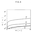
- Fig. 4 there is shown the change in the I D -V D characteristics of the TFT as a function of the energy density of the laser beam irradiation at zero gate potential.
- the abscissa represents the source-to-drain voltage, and the ordinate the source-to-drain current;
- curve 40 shows the I D -V D characteristics for a case without laser beam irradiation of the source and drain semiconductors, and
- curves 41 to 43 show the I D -V D characteristics for the cases in which source and drain semiconductors were irradiated with a laser beam at an energy of 100 mJ/cm 2 , 150 mJ/cm 2 , and 200 mJ/cm 2 , respectively.
- the gate insulating film 5 was formed after activation of the n-type source and drain semiconductors 4. In a practical process, however, the order may be reversed.
- a predetermined pattern etching thereof may be performed thereafter, followed by the activation of the source and the drain areas.
- the presence of the gate insulating film 5 on the I-type semiconductor film 3 may provide further favourable electric properties to the device since the presence thereof prevents degradation of the channel portion caused by laser irradiation.
- the process according to the present invention enables fabrication of a highly reliable TFT in a low temperature process.
- the TFT device moreover is of high performance, is furnished with a source and a drain having high electric conductivity, and is less influenced by parasitic resistances.
- an excimer laser beam can heat only the surface of a device irradiated therewith. Therefore, the substrate of the device is not subject to thermal damage and also a high density multilayered device can be made by the use of an excimer laser beam.
- the process according to the present invention is further advantageous in that the conventional heat treatment at high temperature is omitted.
- the process restrains impurities present in the substrate from penetrating into the active layers. This realizes TFTs having long term stability as regards their electric properties.
- a gate insulating film 5 and a base protective film 2 were provided under the source and the drain contacts 6. Since the same material and the same formation method were used for the films 2 and 5, there is little difference between the coefficients of thermal expansion of the films 2 and 5. Therefore, there is little difference between the thermal expansion of the film 2 and that of the film 5 caused by heat generated during operation of the TFT or by thermal treatments during the fabrication process. Accordingly, there is little risk that a metal electrode, such as an aluminum electrode or the like, provided on the uppermost surface of the device will peel off and become disconnected. Thus, it can be seen that the process according to the present invention provides TFTs which can function for a long period of time with high reliability.
- a silicon oxide film is used as a gate insulating film (gate oxide film), however, a silicon nitride layer or a multi-layer of silicon oxide and silicon nitride may be used as the gate insulating film instead.
- An I-type non-single crystal semiconductor film may be an intrinsic semiconductor film or a substantially intrinsic semiconductor film.
- a substantially intrinsic semiconductor film contains impurities at a concentration less than that of the source and drain n-type semiconductors.
- An irradiation beam for example a light beam or a YAG laser beam or the like, may be used for crystallizing the I-type non-single crystal semiconductor film instead of an excimer laser beam.
- An irradiation beam for example a light beam or a YAG laser beam or the like, may be used for activating the source and drain n-type semiconductors instead of an excimer laser beam.
- the light beam may for example be emitted from a halogen lamp or a Xe lamp.
Landscapes
- Engineering & Computer Science (AREA)
- Physics & Mathematics (AREA)
- Microelectronics & Electronic Packaging (AREA)
- Power Engineering (AREA)
- Condensed Matter Physics & Semiconductors (AREA)
- General Physics & Mathematics (AREA)
- Manufacturing & Machinery (AREA)
- Computer Hardware Design (AREA)
- Optics & Photonics (AREA)
- Chemical & Material Sciences (AREA)
- Crystallography & Structural Chemistry (AREA)
- High Energy & Nuclear Physics (AREA)
- Materials Engineering (AREA)
- Electromagnetism (AREA)
- Health & Medical Sciences (AREA)
- Toxicology (AREA)
- Ceramic Engineering (AREA)
- Thin Film Transistor (AREA)
- Recrystallisation Techniques (AREA)
Description
- The present invention relates to a method for fabricating thin-film transistors (referred to hereinafter as TFTs).
- Thin-film transistors (TFTs) made with non-single crystal semiconductor materials produced by chemical vapor desposition (referred to hereinafter as CVD) processes or the like have recently become of great interest.
- Since such TFTs are deposited on an insulating substrate by a CVD process or the like, the process can advantageously be carried out at a temperature as low as about 500°C or even less. Thus, the process becomes economical, since it allows the use of low-cost soda-lime glass, borosilicate glass, and the like as the substrate.
- TFTs are typically field effect transistors which function in a manner similar to so-called MOSFETs (Metal Oxide Silicon Field-Effect Transistors). As mentioned earlier, TFTs can be deposited at low temperature, and moreover, the maximum area thereof is limited only by the dimensions of the deposition apparatus. Thus, TFTs can be freely and easily scaled up with respect to their area, and this is a great advantage. TFTs are, therefore, promising for use as switching devices for active matrix-structured liquid crystal displays consisting of a large number of pixels (picture elements), as well as for one- or two-dimensional image sensors and the like.
- TFTs may be subjected to fine patterning using the well-established technology of photolithography, and thus they may be integrated in the same manner as, for example, ICs.
- A typical structure of conventional TFTs is schematically shown in Fig. 2 of the accompanying drawings.
- As shown in Fig. 2, a typical thin film transistor comprises an
insulating glass substrate 20, athin film semiconductor 21 consisting of non-single crystal semiconductor material, asource region 22, adrain region 23, asource contact 24, adrain contact 25, agate insulating film 26, and agate contact 27. - In such TFTs, the current between the
source 22 and the drain 23 (the source-to-drain current) can be controlled by applying a voltage to thegate contact 27. - The speed of response of the TFT can be given by the following equation:

- The non-single crystal semiconductor layer used in TFTs comprise numerous grain boundaries and the like, and these have greatly reduced the carrier mobility as compared with that of single crystal semiconductors. The long delay in response ascribed to the low carrier mobility has been a great problem in non-single crystal semiconductor TFTs. TFTs using amorphous silicon (referred to hereinafter as a-Si) semiconductors, in particular, were not practically feasible, since the mobility thereof was so low as in the range of about 0.1 to 1 cm2.V-1.sec-1.
- In order to overcome such problems it is evident from the equation mentioned earlier that in order to increase the speed of response it is required to shorten the channel length or to increase the carrier mobility and many efforts have been made along these lines. It is particularly effective to seek to reduce the channel length, L, since the speed of response increases in proportion to the reciprocal of the square of L.
- In the case of fabricating TFTs on a substrate of large area, however, it is obviously difficult with present photolithographic technology in view of considerations of precision in processing, product yield, production cost, and the like, to reduce the distance between the drain and the source regions (which corresponds approximately to the channel length) to 10 µm or less. In short, no effective means to reduce the channel length of a TFT has yet been established.
- With respect to the possibility of increasing the mobility, µ, of the semiconductor layer itself, there have been taken such measures as to incorporate a polycrystalline semiconductor into the active layer of the TFT. This measure requires relatively high temperature.
- It is also to be noted that in TFTs, the electric current at the channel portion is subject to the materials of which the source and the drain assemblies are made. Thus, the source and the drain assemblies are often made polycrystalline, or some treatment is applied thereto to assure good electric contact with the channel portion.
- More specifically, a thin film of polycrystalline silicon may be deposited by CVD at the source and the drain areas, but the CVD process requires the process to be carried out at a temperature of 500°C or higher. As an alternative process, a treatment may be carried out to assure good contact between the channel portion and the source and the drain. The treatment comprises, after forming semiconductor layers as the drain and the source, introducing therein an n-type or a p-type impurity by ion-implantation, and then heat-treating the drain and the source at a temperature in a range of from 500 to 800°C.
- Both of the processes mentioned above require a relatively high temperature to obtain a favorable TFT; no TFTs produced wholly by low temperature processes are yet available.
- EP-A-0 171 509 discloses a process to improve the crystallinity of thin semiconductor films by an irradiation step.
- EP-A-0 301 463 discloses a conventional TFT obtained by irradiation annealing steps.
- Ion implantation is used for obtaining good electric contacts between the channel and the drain and source regions. However, it is extremely difficult to carry out uniform doping of impurities over a large area by ion implantation. This remains a great hindrance to the future development of large-area liquid-crystal displays and the like.
- With a view to overcoming the problems mentioned earlier, the present invention provides a process according to claim 1 for fabricating TFTs at low temperature, such process comprising crystallizing the channel portion of a TFT, for example by subjecting it to irradiation with an excimer laser, and modifying the electric properties of the source and drain regions of the TFT, for example by subjecting them to irradiation with an excimer laser, independently of the crystallizing of the channel portion. The invention thus provides a two-step laser annealing process for TFTs which is carried out at low temperature.
- The above and further features of the invention are set forth with particularity in the appended claims and, together with the advantages thereof, will be well understood from consideration of the following description given with reference to the accompanying drawings.
-
- Figs. 1(A) to 1(C) schematically show a process for fabricating a TFT according to an exemplary embodiment of the present invention;
- Fig. 2 shows a cross-section of a conventional TFT;
- Fig. 3 is a graph showing the relationship between the conductivity of an n-type layer and laser energy density; and
- Fig. 4 is a graphical diagram showing relationships between ID and VD.
- Fig. 1 schematically illustrates a process for fabricating a planar-type TFT according to an exemplary embodiment of the present invention.
- On the surface of a soda-lime glass substrate 1 there was deposited a 300 nm thick silicon oxide film serving as a base
protective film 2, thefilm 2 being deposited by a well known sputtering method. The film deposition was carried out under the following conditions:Sputter gas 100% O2 Reaction pressure 0.5 Pa RF power 400 W Temperature of the substrate 150°C Rate of film deposition 5 nm/min. - On top of the base
protective film 2 deposited on the substrate there was further deposited an I-type non-single crystal silicon semiconductor film 3 by means of a well-known sputtering process to a film thickness of approximately 100 nm. The film deposition was carried out under the following conditions:Temperature of the substrate 100°C Reaction pressure 0.5 Pa RF power (13.56 MHz) 300 W. - Etching under predetermined conditions was then performed, to thereby obtain an intermediate device structure as shown in Fig. 1(A).
- Then, the film 3 was annealed by irradiation with excimer laser energy so as to crystallize the film 3 into a polycrystal. The conditions of the annealing process were as follows:
Laser energy density 200 mJ/cm2 Pulse repetition 50 shots. - Further, on the film 3 there was deposited a 50 nm thick n-type non-single crystal silicon film doped with phosphorus such film serving as a low-resistance non-single crystal semiconductor layer. The deposition of this film was carried out by plasma chemical vapor deposition under the following conditions:
Gas materials SiH4 + PH3 + H2 Reaction pressure 0.05 Torr Temperature of the substrate 300°C RF power (13.56 MHz) 200 W Film thickness 50 nm. - A microcrystalline film with a low electric resistance may be deposited as the n-type non-single crystal silicon film, by incorporating a large amount of H2 gas into the gas materials at elevated RF power.
- A portion of the n-type non-single crystal silicon film was then removed using conventional photolithography, leaving the source and the
drain areas 4. Thus there was obtained an intermediate device structure as shown in Fig. 1(B). - The n-type non-single crystal semiconductor material of the source and the
drain regions 4 was activated by irradiating the same with an excimer laser beam under the following conditions:Laser energy density 100 mJ/cm2 Pulse repetition 50 shots. - The channel portion 7 was then activated by plasma treatment in hydrogen under the following conditions:
Temperature of the substrate 250°C RF power 100 W Duration of the treatment 60 minutes. - On the activated channel there were thereafter formed, in the order stated, a 100 nm thick
gate oxide film 5, source- and drain- contact holes by etching, and analuminum contact 6, whereby a TFT structure as shown in Fig. 1(C) was obtained. The formation of the gate oxide film was carried out using the same materials and method as those used in the deposition of the baseprotective film 2. The etching of the contact holes was carried out by a method well known in the art. - The conductivity of the source and drain n-type non-single
crystal semiconductor material 4 changes as a function of the energy density of the irradiating excimer laser beam in the manner shown in Fig. 3. - In Fig. 3, the conductivity of the
semiconductor 4 increases with increasing energy density up to 150 mJ/cm2. However, the conductivity can be seen to decrease with further increase of the energy density since the N+ layer surfaces of the source and drain are damaged by high energy laser irradiation. With still further increase of the energy density, the source anddrain semiconductors 4 would sublime. - Therefore, the laser irradiation should be effected at an energy density preferably of 150 mJ/cm2 or less, and more preferably in the range of from 100 mJ/cm2 to 150 mJ/cm2. With laser irradiation with the energy density in the range of from 100 mJ/cm2 to 150 mJ/cm2, a conductivity in the range of from 80 to 200 S/cm can be obtained.
- In case laser beam irradiation with an energy density of 150 mJ/cm2 or less is applied, phosphorus impurities contained in the source and drain 4 do not move from the source and drain 4 to the channel portion because with laser irradiation with such a low energy density as 150 mJ/cm2 or less, the phosphorus impurities stay in the source and
drain 4. Therefore, the channel portion is free from degradation by the phosphorus impurities. - Since the channel portion was well crystallized by the laser annealing of the I-type semiconductor film 3, the channel portion would be degraded by the laser irradiation of the source and
drain semiconductors 4 at an energy density of more than 150 mJ/cm2 if the channel portion were not masked. The degradation is caused by stress which is, in turn, caused by the difference between the temperature of the channel portion and that of the other portions of the film 3 during the laser irradiation of the source and drain. However, even if the laser irradiation of the intermediate device structure as shown in Fig. 1(B) is carried out without masking the channel portion, this laser irradiation can be applied without degrading the channel portion if a not so high energy density of 150 mJ/cm2 or less is applied. - In this connection, in Fig. 4 there is shown the change in the ID-VD characteristics of the TFT as a function of the energy density of the laser beam irradiation at zero gate potential. In the figure, the abscissa represents the source-to-drain voltage, and the ordinate the source-to-drain current;
curve 40 shows the ID-VD characteristics for a case without laser beam irradiation of the source and drain semiconductors, and curves 41 to 43 show the ID-VD characteristics for the cases in which source and drain semiconductors were irradiated with a laser beam at an energy of 100 mJ/cm2, 150 mJ/cm2, and 200 mJ/cm2, respectively. - From Fig. 4, it can be seen that the OFF current between the source and drain is small and the channel portion suffers little degradation in the case of the laser irradiation of the source and drain semiconductors at an energy of 150 mJ/cm2 or lower.
- One might consider crystallizing the I-type semiconductor layer 3 while activating the source and the drain in the same single step by irradiating with a laser beam suitable for both purposes. However, this is not possible because the laser energy density required for the crystallization and that for the activation is different. If the laser beam energy is set to the optimum for the crystallization of the I-type semiconductor layer 3, sublimation of the source and drain n-type semiconductors or damage to the source and drain N+ layer or degradation of the channel might occur as explained earlier; if the energy is set to the optimum for the activation, on the other hand, the I-type semiconductor layer 3 would not crystallize. Thus, laser irradiation in two steps becomes crucial for the process according to the present invention.
- In the above-described embodiment, the
gate insulating film 5 was formed after activation of the n-type source anddrain semiconductors 4. In a practical process, however, the order may be reversed. - That is, after depositing the
gate insulating film 5, a predetermined pattern etching thereof may be performed thereafter, followed by the activation of the source and the drain areas. - In such a case, the presence of the
gate insulating film 5 on the I-type semiconductor film 3 may provide further favourable electric properties to the device since the presence thereof prevents degradation of the channel portion caused by laser irradiation. - Thus, it is clear from the foregoing description that the process according to the present invention enables fabrication of a highly reliable TFT in a low temperature process. The TFT device moreover is of high performance, is furnished with a source and a drain having high electric conductivity, and is less influenced by parasitic resistances.
- Furthermore, an excimer laser beam can heat only the surface of a device irradiated therewith. Therefore, the substrate of the device is not subject to thermal damage and also a high density multilayered device can be made by the use of an excimer laser beam.
- The process according to the present invention is further advantageous in that the conventional heat treatment at high temperature is omitted. Thus, the process restrains impurities present in the substrate from penetrating into the active layers. This realizes TFTs having long term stability as regards their electric properties.
- In the process according to the embodiment of the present invention as set forth earlier, a
gate insulating film 5 and a baseprotective film 2 were provided under the source and thedrain contacts 6. Since the same material and the same formation method were used for thefilms films film 2 and that of thefilm 5 caused by heat generated during operation of the TFT or by thermal treatments during the fabrication process. Accordingly, there is little risk that a metal electrode, such as an aluminum electrode or the like, provided on the uppermost surface of the device will peel off and become disconnected. Thus, it can be seen that the process according to the present invention provides TFTs which can function for a long period of time with high reliability. - The foregoing description of an exemplary embodiment has been presented for purposes of illustration and description. However, it is to be appreciated that the described embodiment is exemplary only and is susceptible to modification and variation without departure from the scope of the invention as determined by the appended claims. For example, in the embodiment described, a silicon oxide film is used as a gate insulating film (gate oxide film), however, a silicon nitride layer or a multi-layer of silicon oxide and silicon nitride may be used as the gate insulating film instead. An I-type non-single crystal semiconductor film may be an intrinsic semiconductor film or a substantially intrinsic semiconductor film. A substantially intrinsic semiconductor film contains impurities at a concentration less than that of the source and drain n-type semiconductors. An irradiation beam, for example a light beam or a YAG laser beam or the like, may be used for crystallizing the I-type non-single crystal semiconductor film instead of an excimer laser beam. An irradiation beam, for example a light beam or a YAG laser beam or the like, may be used for activating the source and drain n-type semiconductors instead of an excimer laser beam. The light beam may for example be emitted from a halogen lamp or a Xe lamp.
Claims (11)
- A method of manufacturing a thin film transistor, said method comprising:forming a non-single crystal semiconductor layer (3) on a substrate (1);crystallizing said non-single crystal semiconductor layer (3) by irradiating the same with a first irradiation beam; andforming source and drain semiconductor layers (4) on the non-single crystal semiconductor layer (3);characterised in that said method further comprises activating the source and drain semiconductor layers (4) by irradiating the same with a second irradiation beam having an energy density which is less than that of said first irradiation beam.
- The method of claim 1 wherein the energy density of said second irradiation beam is 150 mJ/cm2 or less.
- The method of any preceding claim wherein the formation of said source and drain semiconductor layers (4) is carried out by forming a semiconductor layer by chemical vapor deposition and patterning said semiconductor layer to define said source and drain semiconductor layers (4).
- The method of any preceding claim wherein said non-single crystal semiconductor layer (3) comprises an intrinsic or substantially intrinsic semiconductor.
- The method of any preceding claim wherein said step of forming said source and drain semiconductor layers (4) includes forming a channel region in said non-single crystal semiconductor layer (3).
- The method of claim 5 wherein the irradiation of said source and drain layers (4) is carried out without masking said channel region.
- The method of claim 5 further comprising:forming an insulating film (5) on said channel region and said, source and drain layers (4);removing portions of said insulating film (5) to form contact openings through said insulating film (5) at said source and drain layers (4); and whereinsaid step of activating said source and drain layers (4) includes irradiating said source and drain layers and remaining portions of said insulating film (5) with said remaining portions serving as masks.
- The method of claim 7 wherein said insulating film (5) comprises silicon oxide, silicon nitride or a multilayer of silicon oxide and silicon nitride.
- The method of claim 7 or 8 wherein an upper surface of said channel region is entirely covered by said remaining portion.
- The method of any preceding claim wherein said source and drain layers comprise n-type semiconductor material.
- The method of any preceding claim wherein irradiation is effected by use of a laser beam and/or a light beam.
Applications Claiming Priority (2)
| Application Number | Priority Date | Filing Date | Title |
|---|---|---|---|
| JP2145069A JP2700277B2 (en) | 1990-06-01 | 1990-06-01 | Method for manufacturing thin film transistor |
| JP145069/90 | 1990-06-01 |
Publications (3)
| Publication Number | Publication Date |
|---|---|
| EP0459836A2 EP0459836A2 (en) | 1991-12-04 |
| EP0459836A3 EP0459836A3 (en) | 1993-02-24 |
| EP0459836B1 true EP0459836B1 (en) | 1997-09-17 |
Family
ID=15376664
Family Applications (1)
| Application Number | Title | Priority Date | Filing Date |
|---|---|---|---|
| EP91305013A Expired - Lifetime EP0459836B1 (en) | 1990-06-01 | 1991-06-03 | Method for fabricating thin-film transistors |
Country Status (5)
| Country | Link |
|---|---|
| US (3) | US6458200B1 (en) |
| EP (1) | EP0459836B1 (en) |
| JP (1) | JP2700277B2 (en) |
| KR (1) | KR950007355B1 (en) |
| DE (1) | DE69127656T2 (en) |
Cited By (1)
| Publication number | Priority date | Publication date | Assignee | Title |
|---|---|---|---|---|
| US7045399B2 (en) | 1992-12-09 | 2006-05-16 | Semiconductor Energy Laboratory Co., Ltd. | Electronic circuit |
Families Citing this family (14)
| Publication number | Priority date | Publication date | Assignee | Title |
|---|---|---|---|---|
| JP2700277B2 (en) | 1990-06-01 | 1998-01-19 | 株式会社半導体エネルギー研究所 | Method for manufacturing thin film transistor |
| US5930608A (en) | 1992-02-21 | 1999-07-27 | Semiconductor Energy Laboratory Co., Ltd. | Method of fabricating a thin film transistor in which the channel region of the transistor consists of two portions of differing crystallinity |
| JPH06124913A (en) | 1992-06-26 | 1994-05-06 | Semiconductor Energy Lab Co Ltd | Laser treatment |
| US5403762A (en) * | 1993-06-30 | 1995-04-04 | Semiconductor Energy Laboratory Co., Ltd. | Method of fabricating a TFT |
| CN100359633C (en) * | 1992-12-09 | 2008-01-02 | 株式会社半导体能源研究所 | Method of manufacturing semi-conductor device |
| TW425637B (en) | 1993-01-18 | 2001-03-11 | Semiconductor Energy Lab | Method of fabricating mis semiconductor device |
| US6331717B1 (en) | 1993-08-12 | 2001-12-18 | Semiconductor Energy Laboratory Co. Ltd. | Insulated gate semiconductor device and process for fabricating the same |
| JP3173926B2 (en) | 1993-08-12 | 2001-06-04 | 株式会社半導体エネルギー研究所 | Method of manufacturing thin-film insulated gate semiconductor device and semiconductor device thereof |
| US5681760A (en) * | 1995-01-03 | 1997-10-28 | Goldstar Electron Co., Ltd. | Method for manufacturing thin film transistor |
| JP3778456B2 (en) | 1995-02-21 | 2006-05-24 | 株式会社半導体エネルギー研究所 | Method for manufacturing insulated gate thin film semiconductor device |
| JP3917205B2 (en) * | 1995-11-30 | 2007-05-23 | 株式会社半導体エネルギー研究所 | Method for manufacturing semiconductor device |
| US6872607B2 (en) | 2000-03-21 | 2005-03-29 | Semiconductor Energy Laboratory Co., Ltd. | Method of manufacturing a semiconductor device |
| US7291522B2 (en) * | 2004-10-28 | 2007-11-06 | Hewlett-Packard Development Company, L.P. | Semiconductor devices and methods of making |
| JP6003321B2 (en) * | 2012-07-18 | 2016-10-05 | Jfeスチール株式会社 | Method for producing grain-oriented electrical steel sheet |
Citations (2)
| Publication number | Priority date | Publication date | Assignee | Title |
|---|---|---|---|---|
| EP0301463A2 (en) * | 1987-07-27 | 1989-02-01 | Nippon Telegraph And Telephone Corporation | Thin film silicon semiconductor device and process for producing it |
| EP0331811A2 (en) * | 1987-12-18 | 1989-09-13 | Fujitsu Limited | Semiconductor devices with silicon-on-insulator structures |
Family Cites Families (27)
| Publication number | Priority date | Publication date | Assignee | Title |
|---|---|---|---|---|
| US4174217A (en) * | 1974-08-02 | 1979-11-13 | Rca Corporation | Method for making semiconductor structure |
| JPS558026A (en) | 1978-06-30 | 1980-01-21 | Matsushita Electric Ind Co Ltd | Semi-conductor device manufacturing method |
| EP0171509B1 (en) * | 1979-07-24 | 1990-10-31 | Hughes Aircraft Company | Silicon on sapphire laser process |
| US4266986A (en) * | 1979-11-29 | 1981-05-12 | Bell Telephone Laboratories, Incorporated | Passivation of defects in laser annealed semiconductors |
| JPS5785262A (en) * | 1980-11-17 | 1982-05-27 | Toshiba Corp | Manufacture of metal oxide semiconductor type semiconductor device |
| JPS5814524A (en) * | 1981-07-17 | 1983-01-27 | Fujitsu Ltd | Manufacturing semiconductor device |
| JPS58164267A (en) | 1982-03-25 | 1983-09-29 | Seiko Epson Corp | Manufacture of thin film silicon transistor |
| US4769338A (en) * | 1984-05-14 | 1988-09-06 | Energy Conversion Devices, Inc. | Thin film field effect transistor and method of making same |
| US4727044A (en) * | 1984-05-18 | 1988-02-23 | Semiconductor Energy Laboratory Co., Ltd. | Method of making a thin film transistor with laser recrystallized source and drain |
| JPS61135110A (en) * | 1984-12-05 | 1986-06-23 | Fujitsu Ltd | Manufacture of semiconductor device |
| US4933296A (en) * | 1985-08-02 | 1990-06-12 | General Electric Company | N+ amorphous silicon thin film transistors for matrix addressed liquid crystal displays |
| DE3689735T2 (en) * | 1985-08-02 | 1994-06-30 | Semiconductor Energy Lab | Method and device for manufacturing semiconductor devices. |
| JPH07120802B2 (en) * | 1985-08-08 | 1995-12-20 | ソニー株式会社 | Method for manufacturing semiconductor device |
| JPS6239067A (en) | 1985-08-13 | 1987-02-20 | Seiko Instr & Electronics Ltd | Manufacture of thin film semiconductor device |
| JPH0746729B2 (en) * | 1985-12-26 | 1995-05-17 | キヤノン株式会社 | Method of manufacturing thin film transistor |
| JPS62254467A (en) * | 1986-04-28 | 1987-11-06 | Seiko Instr & Electronics Ltd | Manufacture of thin film transistor |
| JPS63200572A (en) | 1987-02-17 | 1988-08-18 | Seiko Instr & Electronics Ltd | Manufacture of thin film semiconductor device |
| JPS63250178A (en) | 1987-04-07 | 1988-10-18 | Seiko Instr & Electronics Ltd | Manufacture of thin film semiconductor device |
| JPS63292682A (en) * | 1987-05-26 | 1988-11-29 | Seiko Instr & Electronics Ltd | Manufacture of thin film semiconductor device |
| US4743567A (en) * | 1987-08-11 | 1988-05-10 | North American Philips Corp. | Method of forming thin, defect-free, monocrystalline layers of semiconductor materials on insulators |
| JPH02130912A (en) | 1988-11-11 | 1990-05-18 | Seiko Epson Corp | Thin film semiconductor device |
| JP2867264B2 (en) * | 1989-02-28 | 1999-03-08 | 株式会社日立製作所 | Liquid crystal display device and manufacturing method thereof |
| JP2832991B2 (en) * | 1989-04-14 | 1998-12-09 | ソニー株式会社 | Multilayer wiring forming method and continuous processing apparatus |
| JP2700277B2 (en) * | 1990-06-01 | 1998-01-19 | 株式会社半導体エネルギー研究所 | Method for manufacturing thin film transistor |
| US5162239A (en) * | 1990-12-27 | 1992-11-10 | Xerox Corporation | Laser crystallized cladding layers for improved amorphous silicon light-emitting diodes and radiation sensors |
| GB9114018D0 (en) * | 1991-06-28 | 1991-08-14 | Philips Electronic Associated | Thin-film transistor manufacture |
| US5424244A (en) * | 1992-03-26 | 1995-06-13 | Semiconductor Energy Laboratory Co., Ltd. | Process for laser processing and apparatus for use in the same |
-
1990
- 1990-06-01 JP JP2145069A patent/JP2700277B2/en not_active Expired - Lifetime
-
1991
- 1991-06-01 KR KR1019910009163A patent/KR950007355B1/en not_active IP Right Cessation
- 1991-06-03 DE DE69127656T patent/DE69127656T2/en not_active Expired - Lifetime
- 1991-06-03 EP EP91305013A patent/EP0459836B1/en not_active Expired - Lifetime
-
1993
- 1993-07-12 US US08/089,650 patent/US6458200B1/en not_active Expired - Lifetime
-
2002
- 2002-02-21 US US10/078,354 patent/US6740547B2/en not_active Expired - Fee Related
-
2004
- 2004-05-25 US US10/852,700 patent/US7018874B2/en not_active Expired - Fee Related
Patent Citations (2)
| Publication number | Priority date | Publication date | Assignee | Title |
|---|---|---|---|---|
| EP0301463A2 (en) * | 1987-07-27 | 1989-02-01 | Nippon Telegraph And Telephone Corporation | Thin film silicon semiconductor device and process for producing it |
| EP0331811A2 (en) * | 1987-12-18 | 1989-09-13 | Fujitsu Limited | Semiconductor devices with silicon-on-insulator structures |
Non-Patent Citations (1)
| Title |
|---|
| Laser annealing of semiconductors, Ed. J.M. Poate et al, Academic Press, 1982 * |
Cited By (6)
| Publication number | Priority date | Publication date | Assignee | Title |
|---|---|---|---|---|
| US7045399B2 (en) | 1992-12-09 | 2006-05-16 | Semiconductor Energy Laboratory Co., Ltd. | Electronic circuit |
| US7061016B2 (en) | 1992-12-09 | 2006-06-13 | Semiconductor Energy Laboratory Co., Ltd. | Electronic circuit |
| US7105898B2 (en) | 1992-12-09 | 2006-09-12 | Semiconductor Energy Laboratory Co., Ltd. | Electronic circuit |
| US7547916B2 (en) | 1992-12-09 | 2009-06-16 | Semiconductor Energy Laboratory Co., Ltd. | Electronic circuit |
| US7897972B2 (en) | 1992-12-09 | 2011-03-01 | Semiconductor Energy Laboratory Co., Ltd. | Electronic circuit |
| US8294152B2 (en) | 1992-12-09 | 2012-10-23 | Semiconductor Energy Laboratory Co., Ltd. | Electronic circuit including pixel electrode comprising conductive film |
Also Published As
| Publication number | Publication date |
|---|---|
| US20030017656A1 (en) | 2003-01-23 |
| EP0459836A3 (en) | 1993-02-24 |
| DE69127656T2 (en) | 1998-04-30 |
| US6458200B1 (en) | 2002-10-01 |
| US20050009254A1 (en) | 2005-01-13 |
| JP2700277B2 (en) | 1998-01-19 |
| KR950007355B1 (en) | 1995-07-10 |
| US7018874B2 (en) | 2006-03-28 |
| US6740547B2 (en) | 2004-05-25 |
| EP0459836A2 (en) | 1991-12-04 |
| DE69127656D1 (en) | 1997-10-23 |
| JPH0437144A (en) | 1992-02-07 |
Similar Documents
| Publication | Publication Date | Title |
|---|---|---|
| KR100333153B1 (en) | Process for fabricating semiconductor device | |
| US5858823A (en) | Semiconductor circuit for electro-optical device and method of manufacturing the same | |
| JP3193803B2 (en) | Manufacturing method of semiconductor element | |
| US7056775B2 (en) | Semiconductor device and process for fabricating the same | |
| US5851860A (en) | Semiconductor device and method for producing the same | |
| KR100280171B1 (en) | Non-single-crystal semiconductor device (thin film transistor), liquid crystal display device using the same and manufacturing method thereof | |
| US5834071A (en) | Method for forming a thin film transistor | |
| EP0459836B1 (en) | Method for fabricating thin-film transistors | |
| JPH0758339A (en) | Semiconductor device and its production | |
| KR20030069779A (en) | Thin film transistor and method for manufacturing thereof | |
| KR100700681B1 (en) | Crystallization of semiconductor thin film and manufacturing method of thin film semiconductor device | |
| JPH07131034A (en) | Fabrication of semiconductor device | |
| JP3347340B2 (en) | Method for manufacturing thin film transistor | |
| JPH04340725A (en) | Manufacture of thin film transistor | |
| JPH0832074A (en) | Semiconductor device and manufacture thereof | |
| JP3380527B2 (en) | Method for manufacturing semiconductor device | |
| JP3181901B2 (en) | Thin film transistor | |
| JP2852855B2 (en) | Method for manufacturing semiconductor device | |
| EP0955674B1 (en) | Fabrication of hybrid polycrystalline and amorphous silicon structures | |
| JPH0831737A (en) | Semiconductor device and manufacture thereof | |
| JPH0982639A (en) | Semiconductor device and its manufacture | |
| JP2789417B2 (en) | Method for manufacturing semiconductor device | |
| JP3316203B2 (en) | Method for manufacturing semiconductor device | |
| JP3181817B2 (en) | Thin film transistor | |
| JPH04305939A (en) | Manufacture of thin-film transistor |
Legal Events
| Date | Code | Title | Description |
|---|---|---|---|
| PUAI | Public reference made under article 153(3) epc to a published international application that has entered the european phase |
Free format text: ORIGINAL CODE: 0009012 |
|
| AK | Designated contracting states |
Kind code of ref document: A2 Designated state(s): DE FR GB |
|
| PUAL | Search report despatched |
Free format text: ORIGINAL CODE: 0009013 |
|
| AK | Designated contracting states |
Kind code of ref document: A3 Designated state(s): DE FR GB |
|
| 17P | Request for examination filed |
Effective date: 19930625 |
|
| 17Q | First examination report despatched |
Effective date: 19941024 |
|
| GRAG | Despatch of communication of intention to grant |
Free format text: ORIGINAL CODE: EPIDOS AGRA |
|
| GRAH | Despatch of communication of intention to grant a patent |
Free format text: ORIGINAL CODE: EPIDOS IGRA |
|
| GRAH | Despatch of communication of intention to grant a patent |
Free format text: ORIGINAL CODE: EPIDOS IGRA |
|
| GRAA | (expected) grant |
Free format text: ORIGINAL CODE: 0009210 |
|
| AK | Designated contracting states |
Kind code of ref document: B1 Designated state(s): DE FR GB |
|
| REF | Corresponds to: |
Ref document number: 69127656 Country of ref document: DE Date of ref document: 19971023 |
|
| ET | Fr: translation filed | ||
| PLBE | No opposition filed within time limit |
Free format text: ORIGINAL CODE: 0009261 |
|
| STAA | Information on the status of an ep patent application or granted ep patent |
Free format text: STATUS: NO OPPOSITION FILED WITHIN TIME LIMIT |
|
| 26N | No opposition filed | ||
| REG | Reference to a national code |
Ref country code: GB Ref legal event code: IF02 |
|
| PGFP | Annual fee paid to national office [announced via postgrant information from national office to epo] |
Ref country code: FR Payment date: 20100709 Year of fee payment: 20 |
|
| PGFP | Annual fee paid to national office [announced via postgrant information from national office to epo] |
Ref country code: GB Payment date: 20100602 Year of fee payment: 20 Ref country code: DE Payment date: 20100526 Year of fee payment: 20 |
|
| REG | Reference to a national code |
Ref country code: DE Ref legal event code: R071 Ref document number: 69127656 Country of ref document: DE |
|
| REG | Reference to a national code |
Ref country code: DE Ref legal event code: R071 Ref document number: 69127656 Country of ref document: DE |
|
| REG | Reference to a national code |
Ref country code: GB Ref legal event code: PE20 Expiry date: 20110602 |
|
| PG25 | Lapsed in a contracting state [announced via postgrant information from national office to epo] |
Ref country code: GB Free format text: LAPSE BECAUSE OF EXPIRATION OF PROTECTION Effective date: 20110602 |
|
| PG25 | Lapsed in a contracting state [announced via postgrant information from national office to epo] |
Ref country code: DE Free format text: LAPSE BECAUSE OF EXPIRATION OF PROTECTION Effective date: 20110604 |