EP1209772A2 - Kontakt zum Unterbinden einer Bogenentladung, Verfahren zum Herstellen desselbigen und Verbinder zum Unterbinden einer Bogenentladung - Google Patents
Kontakt zum Unterbinden einer Bogenentladung, Verfahren zum Herstellen desselbigen und Verbinder zum Unterbinden einer Bogenentladung Download PDFInfo
- Publication number
- EP1209772A2 EP1209772A2 EP01128142A EP01128142A EP1209772A2 EP 1209772 A2 EP1209772 A2 EP 1209772A2 EP 01128142 A EP01128142 A EP 01128142A EP 01128142 A EP01128142 A EP 01128142A EP 1209772 A2 EP1209772 A2 EP 1209772A2
- Authority
- EP
- European Patent Office
- Prior art keywords
- terminal
- contact
- conductive layer
- male
- main body
- Prior art date
- Legal status (The legal status is an assumption and is not a legal conclusion. Google has not performed a legal analysis and makes no representation as to the accuracy of the status listed.)
- Granted
Links
Images


Classifications
-
- H—ELECTRICITY
- H01—ELECTRIC ELEMENTS
- H01R—ELECTRICALLY-CONDUCTIVE CONNECTIONS; STRUCTURAL ASSOCIATIONS OF A PLURALITY OF MUTUALLY-INSULATED ELECTRICAL CONNECTING ELEMENTS; COUPLING DEVICES; CURRENT COLLECTORS
- H01R13/00—Details of coupling devices of the kinds covered by groups H01R12/70 or H01R24/00 - H01R33/00
- H01R13/02—Contact members
- H01R13/03—Contact members characterised by the material, e.g. plating, or coating materials
- H01R13/035—Plated dielectric material
-
- H—ELECTRICITY
- H01—ELECTRIC ELEMENTS
- H01R—ELECTRICALLY-CONDUCTIVE CONNECTIONS; STRUCTURAL ASSOCIATIONS OF A PLURALITY OF MUTUALLY-INSULATED ELECTRICAL CONNECTING ELEMENTS; COUPLING DEVICES; CURRENT COLLECTORS
- H01R13/00—Details of coupling devices of the kinds covered by groups H01R12/70 or H01R24/00 - H01R33/00
- H01R13/648—Protective earth or shield arrangements on coupling devices, e.g. anti-static shielding
- H01R13/6485—Electrostatic discharge protection
-
- H—ELECTRICITY
- H01—ELECTRIC ELEMENTS
- H01R—ELECTRICALLY-CONDUCTIVE CONNECTIONS; STRUCTURAL ASSOCIATIONS OF A PLURALITY OF MUTUALLY-INSULATED ELECTRICAL CONNECTING ELEMENTS; COUPLING DEVICES; CURRENT COLLECTORS
- H01R13/00—Details of coupling devices of the kinds covered by groups H01R12/70 or H01R24/00 - H01R33/00
- H01R13/02—Contact members
- H01R13/04—Pins or blades for co-operation with sockets
-
- H—ELECTRICITY
- H01—ELECTRIC ELEMENTS
- H01R—ELECTRICALLY-CONDUCTIVE CONNECTIONS; STRUCTURAL ASSOCIATIONS OF A PLURALITY OF MUTUALLY-INSULATED ELECTRICAL CONNECTING ELEMENTS; COUPLING DEVICES; CURRENT COLLECTORS
- H01R13/00—Details of coupling devices of the kinds covered by groups H01R12/70 or H01R24/00 - H01R33/00
- H01R13/02—Contact members
- H01R13/10—Sockets for co-operation with pins or blades
Definitions
- This invention relates to a connector for use in a wire harness in an automotive vehicle, and a terminal for use in such a connector.
- a male terminal has a bar-like or a plate-like shape with a lead end thereof tapered in order to facilitate insertion into a female terminal. Every time the male terminal is disengaged from and engaged into the female terminal, arc discharge occurs. The repeated engagement and disengagement causes to melt the tapered lead end of the male terminal due to repeated arc discharges. The melted part of the male terminal is cooled to solidify, accompanied with shifting of the melted part slightly toward a base end thereof. As a result, the tapered lead end of the male terminal disappears accompanied by increase of a diameter thereof. In other words, the terminal is likely to be deformed due to melting by repeated arc discharges , which may result in contact failure with the female terminal or, in a worse case, difficulty or inability of insertion into the female terminal.
- a terminal has a region having a last contact part with a counterpart terminal when the terminal is disengaged from the counterpart terminal.
- the region is formed with an insulating section.
- a conductive section is formed on a surface of the insulating section. The conductive section is electrically connectable to the counterpart terminal.
- the terminals are electrically connectable until the counterpart terminal is detached from the conductive section of the terminal, and arc discharge can be remarkably suppressed by the insulating section. Thus, deformation of the terminal can be effectively suppressed.
- a terminal and a connector embodying the invention are described in detail with reference to the accompanying drawings. Described is first a terminal embodying the invention.
- FIGS. 1A and 1B are side views each schematically showing an example of the inventive terminal.
- FIG. 2 is a partially enlarged sectional view of a male terminal in accordance with the first embodiment of the invention.
- FIG. 3 is a partially enlarged sectional view showing a state that the male terminal is engaged with a female terminal.
- FIG. 4 is an enlarged sectional view showing a state that the male terminal is about to be disengaged from the female terminal.
- the male terminal 1 includes a box-like part 1b constituting a main body of the terminal, and a male electric contact part (male tab) 1a which projects axially forwardly from the box-like part 1b.
- the entirety of the terminal main body is made of a material having a high conductivity such as copper metal.
- the male terminal 1 and a housing 3 made of resin which is adapted to accommodate the male terminal 1 therein constitutes a male connector.
- a female terminal 2 includes a box-like part 2b.
- a contact spring 2a and a second contact piece 2a' are provided in the box-like part 2b in such a manner that the second contact piece 2a' opposes the contact spring 2a to sandwich the male tab 1b therebetween in an engagement of the male terminal 1 and the female terminal 2.
- the female terminal 2 is housed in a housing 4 made of resin.
- the female terminal 2 and the housing 4 constitutes a female connector.
- engaging the terminals 1 and 2 enables to render the male tab 1a into contact with a female electric contact part 2A including the contact spring 2a and the second contact piece 2a', thereby allowing the terminals 1 and 2 to be electrically connectable.
- arc is likely to be discharged at and/or around a contact portion between the male tab 1a and the female contact part 2A.
- the male tab 1a is first detached from the contact spring 2a, and then is detached from the second contact piece 2a'.
- arc is discharged at and/or around a contact portion between the male terminal 1 and the female terminal 2, which may likely to damage the terminals 1 and 2.
- the male terminal 1 is so constructed that an insulating layer 1c (see FIGS. 2 and 4) is formed at an outer region of the male terminal 1 including a distal end part 1e (hereinafter, also referred to as "final-contact part 1e") which corresponds to a part of the male terminal 1 in contact with the female terminal 2 at a final stage of disengagement. Further, the male terminal 1 is so constructed that a conductive layer 1d covers the entirety of the insulating layer 1c. The conductive layer 1d is electrically connected to a primary part (conductive part) of the male terminal 1.
- Covering the final-contact part 1e with the insulating layer 1c and the conductive layer 1d as mentioned above enables to keep the male terminal 1 electrically connectable with the female terminal 2 by way of the conductive layer 1d until the male terminal 1 is completely disengaged from the female terminal 2. Also, even in the case where arc is discharged at the disengagement of the male terminal 1 from the female terminal 2, the insulating layer 1c formed on the inner side of the conductive layer 1d effectively lowers the amount of discharged arc to thereby securely suppress deformation of the male terminal 1 and the female terminal 2.
- the present invention is effective for the following reasons in the aspect of suppressing arc discharge and deformation of terminals.
- the tab part of the male terminal is likely to be deformed by discharged arc.
- the male terminal is coated with the insulating layer and the conductive layer, even if arc is discharged, damage is restricted to the outer surface of the conductive layer. Since it is less likely that the primary part of the tab may be deformed because the primary part of the tab is located on the inner side of the insulating layer, a desirable engagement of the terminals is maintained.
- the insulating layer 1c may preferably be formed at least at the final-contact part 1e.
- a site for forming the insulating layer 1c on the final-contact part 1e of the male terminal 1 is not limited to the one as illustrated. However, it is preferable not to form an insulating layer on a certain part of the male terminal 1 which is rendered into contact with the female terminal 2 during an engagement.
- the male tab 1a is in contact with the contact spring 2a and the second contact piece 2a' in a securely engaged state of the male terminal 1 and the female terminal 2.
- Parts of the male terminal 1a which are rendered into contact with the contact spring 2a and the second contact piece 2a' are respectively referred to as "contact part 1f" and "contact part 1f'".
- the insulating layer 1c is not formed on the contact parts 1f and 1f' (entire region of the contact part 1f and a base region of the contact part 1f' in FIG. 3).
- non-formation of the insulating layer 1c on the certain part of the male terminal 1 which is rendered into contact with the female terminal 2 in an engagement enables to render the male terminal 1 in direct contact with the female terminal 2 or in indirect contact therewith via the conductive layer 1d. Thereby, there is no likelihood of lowering conductivity of the connectors in an engagement of the terminals.
- the insulating layer 1c is generally formed on a certain region including the final-contact part 1e of the male terminal 1. It is preferable to form the insulating layer 1c on the following region:
- Forming the insulating layer 1c on the above region enables to securely prevent arc from being discharged around the terminal beyond the insulating layer 1c.
- a distal end 1g or its vicinity constitutes the final-contact part.
- the insulating layer 1c having an axial length of 1mm or longer, preferably 3mm or longer from the distal end 1g.
- the material of forming the insulating layer 1c is not limited, as far as the material is effective to suppress arc discharge as low as possible.
- the insulating layer 1c includes layers processed with metallic deposition such as Al 2 O 3 (alumite)-layer, SiO 2 -layer, Si 3 N 4 -layer, TiO 2 -layer, metallic insulating layers such as layers applied with black color coating (CuO-layer), layers processed with chromate, and resinous insulating layers made of insulating resins.
- the metallic layer is not necessarily formed by vapor deposition, and may be formable by metal plating, adhering a thin metallic film on the terminal, or its equivalent.
- the resinous insulating layer may be formed by applying a coating agent (paint coating, enamel coating, varnished coating, etc.) in which an insulating resin is dissolved in a solvent onto the terminal according to various coating techniques (including spray coating and dipping). A baking process may be added when need arises to do so. Alternatively, the insulating resin may be applied in powdery state, or an insulating film may be adhered on the terminal.
- a coating agent paint coating, enamel coating, varnished coating, etc.
- various coating techniques including spray coating and dipping
- a baking process may be added when need arises to do so.
- the insulating resin may be applied in powdery state, or an insulating film may be adhered on the terminal.
- the thickness of the insulating layer 1c ranges from 0.5 to 500 ⁇ m, preferably from 5 to 50 ⁇ m.
- the insulating layer 1c has an electric resistance of 1 ⁇ 10 16 ⁇ or greater.
- Providing the insulating layer with an electric resistance larger than that of a metal (silver metal) constituting a tab part of the terminal enables to reduce arc discharge.
- the insulating layer may be electrically conductive to a certain extent as far as arc discharge is suppressed.
- the electric resistance of the insulating layer may be, for example, 1 ⁇ or larger, preferably 20 ⁇ or larger.
- a site for forming the conductive layer 1d is not specifically limited, as far as the conductive layer 1d covers the insulating layer 1c. Generally, it is preferable to form the conductive layer 1d over a region covering at least 0.1mm in axial length (preferably, at least 1mm in axial length) from an outermost (most upstream) end position in the terminal insertion direction in order to securely render the conductive layer 1d electrically connectable with the terminal 1.
- the entirety of the male terminal 1 may be covered with the conductive layer 1d.
- the conductive layer 1d may preferably be formed over a region covering 3mm in axial length at longest from the most upstream end position of the insulating layer 1c in the terminal insertion direction.
- the conductive layer may be a layer plated with a conductive metal such as Sn, Ni, Al, Ag, and Au, or a conductive polymer layer such as a polyaniline layer which is doped with an alkali metal.
- a metallic layer is formed by plating a metal
- the resultant metallic layer may have a smaller strength at a portion where electroless plating has been performed.
- the conductive layer may preferably be a thin film (for example, 500 ⁇ m or less in thickness, preferably 100 ⁇ m or less, more preferably 35 ⁇ m or less).
- the conductive layer generally has a thickness of 0.01 ⁇ m or greater, preferably, 0.1 ⁇ m or greater.
- the combination of the insulating layer 1c and the conductive layer 1d is not limited to the aforementioned example. Not only the arrangement in which the conductive layer 1d directly covers the insulating layer 1c but also the arrangement in which the conductive layer 1d indirectly covers the insulating layer 1c is applicable. In the case of indirect covering, an intermediate layer is provided between the insulating layer 1c and the conductive layer 1d to indirectly cover the insulating layer 1c with the conductive layer 1d.
- exemplified combinations are described.
- An insulating layer and a conductive layer may be formed on the female terminal, or alternatively, formed on both of the male terminal and the female terminal.
- the second contact piece 2a' may correspond to a final-contact part 2e of the female terminal 2 which corresponds to the final-contact part 1e of the male terminal 1.
- an insulating layer and a conductive layer may be formed on a region including the final-contact part 2e.
- the contact spring 2a may correspond to the final-contact part 1e.
- the contact spring 2a may be formed with an insulating layer and a conductive layer.
- the terminal since the final-contact part is covered with the insulating layer, arc discharge, even if occurs, immediately disappears. Thus, damage due to arc discharge is restricted within a region where the conductive layer is formed, and a terminal is prevented from damage. Even if part of the conductive layer is damaged or broken, which may result in exposure of the insulating layer, the terminal is usable for a certain number of times (e.g., 3 to 200 times) until the conductive layer is almost completely peeled off because the remaining part of the conductive layer makes the terminal electrically conductive while blocking arc discharge thereat.
- a certain number of times e.g., 3 to 200 times
- the conductive layer is completely peeled off at a detachment of the terminals for maintenance and repair of an automotive vehicle even if a high voltage is applied to the wire harness.
- the male terminal 1 may be integrally formed of a single material. In such a case, however, a masking process is required to partially provide the insulating layer 1c on a restricted region such as a lead end part of the male tab 1a, as shown in FIG. 1. Further, it is preferable to etch the surface of the insulating layer 1c to form a desirable conductive layer (plated layer) 1d on the insulating layer 1c. However, in the case where the insulating layer 1c is provided on the integrally formed one-piece male terminal 1, it is extremely difficult to etch the surface of the insulating layer 1c without corroding the main part of the male terminal 1.
- a male terminal by two parts, as shown in FIG. 5, in such a manner that a terminal main body and a terminal lead portion which are independently provided are assembled together.
- the male terminal 101 is constructed by the terminal main body 112 and the terminal lead portion 111.
- the terminal main body 112 is made of a single metallic plate similar to a known terminal except that an electric contact part 112b is formed at a frontal end thereof to be engaged with the terminal lead portion 111.
- the electric contact part 112b has a flat rectangular opening in cross section, and is formed with engaging holes 112d at respective opposite side portions thereof.
- the terminal lead portion 111 includes a tab portion 111a which corresponds to the male tab 1a of the terminal 1 in the first embodiment.
- An engaging portion 111b projects rearwardly from an intermediate portion of a rear wall of the tab portion 111a.
- Engaging arms 111c extend rearwardly from side ends of the rear wall of the tab portion 111a in parallel with opposite side walls of the engaging portion 111b.
- a projection 111d is formed at an outer side of a rear end of the engaging arm 111c (111c).
- the engaging portion 111b and the engaging arm 111c each has such a thickness (height) to be fitted in the opening of the electric contact part 112b.
- an electric conductive layer 101d is formed on a surface of a primary part of the terminal lead portion 111 composed of an insulating material.
- the terminal lead portion 111 is, for example, produced by integrally molding the primary part and by etching the surface thereof to form the conductive layer 101d. In this way, the terminal lead portion 111 is manufactured in a simplified manner without a masking process.
- the material having a high heat resistance for the primary part of the terminal lead portion 111 such as ceramic materials including alumina and aluminum nitride, thermosetting resins including epoxy resins and phenol resins, and thermoplastic resins including polyetheretherketone (PEEK) and polyphenylenesulfide (PPS).
- Metallic plating may include, similar to the first embodiment, electroless plating by copper and nickel, or combination of electroless plating with electrolytic plating or hot dipping with tin or the like. Alternatively, vapor deposition, coating with a conductive coating, adhesion of a metallic film or a conductive film, metallic coating, baking or its equivalent may be applicable in place of the metal plating.
- the primary part of the terminal lead portion 111 is not necessary required to be a single molded member of an insulating material.
- an insulating layer may be provided by forming an oxide film on the surface of the primary part made of, e.g., aluminum or copper.
- Alternative means such as resin coating or enamel baking may be applicable. Molding the entirety of the primary part of the terminal lead portion 111 with an insulating material as mentioned above enables to provide the arc-discharge free terminal 101 without a possibility of breakage or damage of the insulating layer. This arrangement is advantageous in decreasing the number of processes to produce the terminal 101 because this arrangement eliminates necessity of forming an insulating layer independently.
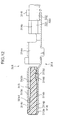
- FIGS. 7 and 8 show a third embodiment of the invention in which a male terminal 201 and a female terminal 202 each has a cylindrical electric contact part.
- the male terminal 201 is divided into a terminal lead portion 211 and a terminal main body 212.
- the terminal lead portion 211 is constructed by integrally forming a cylindrical electric contact part 211f and a coupling shaft 211e which extends rearwardly from the electric contact part 211f and has a smaller diameter than that of the electric contact part 211f.
- a lead end 211g of the electric contact part 211f is tapered in the shape of a truncated cone.
- the terminal main body 212 includes a cylindrical electric contact part 212e and a coupling shaft 212f in the form of a barrel and a wire casing 212g in the form of a barrel.
- the electric contact part 212e has such an inner diameter as to fittingly insert the coupling shaft 211e, and an outer diameter substantially equal to the outer diameter of the electric contact part 211f. Fittingly inserting the coupling shaft 211e axially into a hollow portion of the electric contact part 212e toward the wire casing 212g enables to integrally joint the terminal main body 212 with the terminal lead portion 211. In this state when a wire (not shown) is securely held in the wire casing 212g, the wire is electrically connectable to the male terminal 201.
- the female terminal 202 includes a cylindrical electric contact part 202d into which the electric contact parts 211f, 212e are fittingly inserted.
- a conductor casing 202f and an insulator casing 202g are provided in this order of the female terminal 202 at a downstream end in the terminal insertion direction shown by the arrow in FIG. 8.
- Composing a surface region of at least a primary part of the terminal lead portion 211 of an insulating material and forming a conductive layer over the insulating region enables to provide the female terminal 202 with arc discharge suppression function in the similar manner as the male terminal 201.
- the lead end 211g of the electric contact part 211f formed with a thin conductive layer corresponds to a final-contact part which is rendered in contact with the electric contact part 202d at a final stage of disengagement. Since the lead end 211g has a truncated conical shape, arc discharge which is liable to be generated at a time of disengagement is effectively suppressed, thereby protecting the male terminal 201 from breakage or damage due to arc discharge.
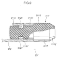
- the coupling construction of the terminal lead portion 211 and the terminal main body 212 is not limited to the one illustrated in FIG. 7. As an altered arrangement, as shown in FIG. 9, a recessed part 211h may be formed in an outer circumference of the coupling shaft 211e of the terminal lead portion 211, and an engaging piece 212h formed on the outer circumferential wall of the cylindrical electric contact part 212e of the terminal main body 212 may be pressingly inserted in the groove 211h.
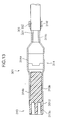
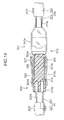
- a fourth embodiment of the invention is described with reference to FIGS. 10 through 20.
- the fourth embodiment is similar to the second embodiment and the third embodiment in that a male terminal 301 is divided into a terminal lead portion 313 and a terminal main body 314.
- the male terminal 301 is constructed in such a manner that a primary part of a terminal lead portion 313 is integrally molded of an insulating material such as synthetic resin and a conductive layer 301d is formed on the insulating surface of the primary part by plating or its equivalent.
- a head portion 313a having a generally rectangular parallelepiped shape and an engaging portion 313b extending rearwardly from the head portion 413a are integrally molded to form an entire configuration of the terminal lead portion 313.
- the sectional surface area of the engaging portion 313b is smaller than that of the head portion 313a.
- An axially extending recessed portion 313c is formed in a half rear portion on the top surface of the head portion 313a toward the engaging portion 313b.
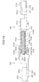
- the terminal main body 314 is constructed by bending a metallic plate having a high conductivity into a certain shape.
- a cylindrical (in FIG. 10, a generally prism-shaped) electric contact part 314b extends forwardly from a box-shaped main part 314a, and the engaging portion 313b of the terminal lead portion 313 is fixedly held in the electric contact part 314b.
- a recessed portion 313d (see FIG. 12) is formed in a rear part on a bottom surface of the engaging portion 313b, and an upwardly and rearwardly projecting engaging piece 314d is formed at a rear part on a bottom wall of the electric contact part 314b. Fittingly inserting the engaging piece 314d in the recessed portion 313d enables to engage the terminal lead portion 314 with the terminal main body 313.
- a tongue-like piece 314t extends along the bottom wall of the electric contact part 314b to support the head portion 313a of the terminal lead portion 313 from below.
- a spring contact piece 314c extends forwardly from a top wall of the electric contact part 314b.
- a frontal end of the spring contact piece 314c is flexible (resiliently deformable), and a projection (contact) 314p projects downwardly from a lower surface of the lead end of the electric contact part 314b.
- the spring contact piece 314c comes into sliding contact with the recessed portion 313c of the terminal lead portion 313, and the projection (contact) 314p formed at the lead end of the spring contact piece 314c is rendered into pressing contact with the conductive layer 301d formed on the lead part on the bottom surface of the recessed portion 313c in a state that the lead end of the spring contact piece 314c is upwardly deformed.
- the terminal main body 314 is provided with a conductor casing 314e and an insulator casing 314f in this order rearwardly from the main part 314a.
- the conductor casing 314e has such a shape as to crimp a center conductor wire 331 (see FIG. 11) which is exposed from a lead end of an insulating wire 330. Thereby, the center conductor wire 331 and the terminal main body 314 are electrically connected.
- the insulator casing 314f has such a shape as to crimp an insulated part 332 of the insulating wire 330 at a rear position from the center conductor wire 331.
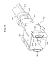
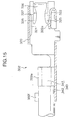
- the female terminal 302 which is engageable with the male terminal 301 is shown in FIGS. 14 through 16.
- the female terminal 302 is formed by bending a metallic plate having a high conductivity into a certain shape in the similar manner as the terminal main body 314 of the male terminal 301.
- the female terminal 302 is constructed in such a manner that a box-shaped electric contact part 320, a conductor casing 302e, and an insulator casing 302f which are formed rearwardly in this order from the electric contact part 320 are integrally formed.
- the conductor casing 302e and the insulator casing 302f have such a shape as to crimp a center conductor wire 341 and an insulating part 342 of an insulating wire 340, respectively.
- the electric contact part 320 is formed with a projection 321 (see FIG. 15) axially extending on a lower surface of a top wall thereof.
- the projection 321 serves as an electric contact member against the male terminal 301.
- a substantially U-shaped spring contact piece 322 is formed on a lead end on the bottom wall of the electric contact part 320 with a free end directed rearwardly.
- a projection (contact) 322a is formed on the upper surface of a rear end portion (deformable free end portion) of the spring contact piece 322.
- the male terminal 302 is inserted in the electric contact part 320 in such a manner that the male terminal 301 is rendered into pressing contact with the projection 322a and the projection 321.
- the female terminal 302 has a feature that a fixed contact piece 324 and a spring contact piece 326 extend forwardly respectively from opposite side walls of the electric contact part 320 to constitute a contact portion for releasing generated arc.
- the fixed contact piece 324 extends forwardly from the left side wall of the electric contact part 320, and is formed with an inward projection 324a at a front end thereof.
- a slit member 325 encloses an upper portion, a lower portion, and part of a front portion of the spring contact piece 326.
- a front end of the spring contact piece 326 is slightly tilted inwardly in such a manner that the front end is flexible sideways.
- the front half portion of the slit member 325 made of a metallic plate is bent rearwardly at about 180° and constitutes a protecting plate portion 327 to protect the spring contact piece 326 from an external force.
- the spring contact piece 326 and the fixed contact piece 324 securely nips the male terminal 301 inwardly in sideways directions.
- the spring contact piece 322 of the electric contact part 320 of the female terminal 302 is deformable downwardly in a state that the male terminal 301 and the female terminal 302 are completely engaged.
- the projection 322a of the spring contact piece 322 and the projection 321 securely hold the electric contact part 314 of the male terminal 401 vertically.
- the projection 322a and the projection 321 are rendered into pressing contact with the bottom wall and the top wall of the electric contact part 314, respectively due to a resilient force of the spring contact piece 322.
- the terminals 301 and 302 are electrically connectable via the pressing contact portion of the electric contact part 314.
- the male terminal 301 is constructed in such a manner that the projection 314p of the spring contact piece 314c is rendered into pressing contact with the conductive layer 301d formed on the surface of the terminal lead portion 313 due to a resilient force of the spring contact piece 314c of the terminal main body 314 against the conductive layer 301d.
- the conductive layer 301d and the terminal main body 314 are electrically connectable by the pressing contact of the spring contact piece 314c against the conductive layer 301d.
- the spring contact piece 414c which is designed to secure electric connection with the terminal lead portion 313, and the engaging portion (engaging piece 314d) which is designed to mechanically engage with the terminal lead portion 313 are formed independently. In this arrangement, since the contact spring piece 314c is free from a mechanical load, the electric connection of the male terminal and the female terminal can be secured while suppressing deformation of the contact spring piece 314c.
- the terminal main body 314 is contacted with the conductive layer 301d at the projection 314p (contact site) which is formed at the frontal end of the spring contact piece 314c, and the spring contact piece 314c is connected to the terminal main body 314 via the rear end thereof.
- a male terminal 1 and a female terminal 2 shown in FIGS. 1 to 4 were produced.
- An intermediate layer (not shown) was formed by subjecting a nickel plate to electroless plating.
- Example 2 This experiment was performed in the similar manner as Example 1 except that a conductive layer and an intermediate layer and an insulating layer were not formed.
- Time duration of arc discharge occurrence was measured in the similar manner as Example 1. It was verified that time duration of arc discharge was about one second. After the arc discharge, the lead end of the male terminal was rounded.
- the invention is advantageous in effectively suppressing deformation and damage of terminals by suppressing arc discharge occurrence at a detachment of the terminals.
- an inventive arc discharge suppressive a terminal is rendered into an electrically connectable state with a counterpart terminal by engaging with the counterpart terminal.
- the terminal comprises a region having a last contact part with the counterpart terminal when the terminal is disengaged from the counterpart terminal, and means for preventing the terminal from being damaged by arc discharge liable to occur in the region.
- the region is formed with an insulating section, and the conductive section is formed on a surface of the insulating section, the conductive section being electrically connectable to the counterpart terminal.
- the insulating section may be preferably formed on at least an outer portion of the terminal including a region corresponding to a last contact part of the terminal which is rendered into contact with the counterpart terminal at a final stage of disengagement of the terminals.
- the conductive layer may be preferably formed on an upper surface of the insulating member to be electrically connectable to a main body of the terminal. The conductive layer is formed at such a location as to be detached from the counterpart terminal at the final stage of disengagement.
- the arc discharge suppressive terminal may be formed of an integral member.
- the terminal may be a two-piece member constructed in such a manner that a terminal lead portion is jointed to a terminal main body made of a conductive member at a front end of the terminal main body.
- the terminal lead portion may include a primary part with at least a surface thereof made of an insulating material, and a conductive layer may be formed on the surface of the primary part to be electrically connected to the terminal main body.
- the terminal is constructed by the terminal main body made of a conductive member and the terminal lead portion including an insulating member, parts for constituting the terminal (particularly, terminal main body) can be mass-produced, and production thereof is facilitated.
- a resiliently deformable spring contact portion is formed on the terminal main body in such a manner as to be rendered into pressing contact with the conductive layer of the terminal lead portion in a resiliently deformed state.
- the spring contact portion can be securely contacted to the conductive layer of the terminal lead portion by utilizing a biasing force due to resilient deformation of the spring contact portion.
- the connection of the conductive layer of the terminal lead portion and the terminal main body can be secured.
- the terminal it is preferable to configure the terminal in such a manner that the spring contact portion has a rear end thereof connected to the terminal main body and a front end thereof which is made into a resiliently deformable free end, and the front end is rendered into contact with the conductive layer of the terminal lead portion in a state that the front end is resiliently deformed.
- the contact position of the spring contact portion with the conductive layer of the terminal lead portion can be closer to a position (generally, a lead most end position) where arc discharge is likely to generate on the conductive layer.
- a position generally, a lead most end position
- heated state of the conductive layer between the aforementioned positions can be effectively suppressed.
- the terminal main body is formed with an engaging portion engageable with the terminal lead portion and the spring contact portion is formed at a position independently of the engaging portion.
- a mechanical connecting site (engaging portion) for mechanically connecting the terminal main body to the terminal lead portion and an electrical connecting site (spring contact portion) are independently provided.
- At least part of a contact portion of the terminal in contact with the counterpart terminal in an engagement with the counterpart terminal may include a non-formation area of the insulating layer to render the terminal into direct contact with the counterpart terminal or indirect contact with the counterpart terminal via the conductive layer.
- the conductive layer may be made of a thin film.
- a pair of terminals include an arc discharge suppressive male terminal and a female terminal engageable with the male terminal.
- the terminal pair is constructed in such a manner that an electric contact part of the female terminal is rendered into contact with a conductive layer non-formation area on the main body of the male terminal in a state that the male terminal and the female terminal are in a completely engaged state.
- the female terminal may be provided with a contact portion which is rendered into contact with the male terminal at a forward position from the electric contact part in a terminal disengaging direction, and the contact portion is provided at such a position that the contact portion is detached from the conductive layer of the male terminal after the electric contact part is detached therefrom when the male terminal is disengaged from the female terminal to suppress arc discharge.
- a spring contact piece is formed at a front end of the female terminal, the spring contact piece has a front end resiliently deformable, and the front end of the spring contact piece is so configured as to be rendered into contact with the conductive layer of the male terminal in a state that the front end of the spring contact piece is resiliently deformed.
- arc discharge can be performed at a position forwardly away from the female terminal main body.
- This arrangement is advantageous in that the female terminal can be securely protected and that the contact between the spring contact piece and the conductive layer can be secured by utilizing a resilient force due to resilient deformation of the spring contact piece for arc discharge.
- a connector comprises the arc discharge suppressive terminal as mentioned above and a housing for accommodating the terminal therein.
- an inventive method for manufacturing an arc discharge suppressive terminal which is rendered into an electrically connectable state by engaging with a counterpart terminal comprises the steps of: producing a terminal main body made of a conductive material; producing a terminal lead portion including a primary part with at least a surface thereof made of an insulating material and a conductive layer which is formed on the surface of the primary part; and jointing the terminal lead portion to the terminal main body at a front end of the terminal main body in such a manner that the conductive layer is detached from the counterpart terminal at a final stage of disengagement of the terminal from the counterpart terminal.
- the terminal main body made of a conductive material and the terminal lead portion including an insulating material are independently produced, and then, the terminal main body and the terminal lead portion are jointed together to assemble the entirety of the terminal.
- This arrangement enables to mass-produce respective parts with ease. Accordingly, compared to a method in which an insulating layer and a conductive layer are provided on a predetermined region on a lead portion of a terminal which is integrally molded, the production process is simplified and productivity can be remarkably improved.
- the step of producing the terminal lead portion includes a step of producing the primary part of the terminal lead portion, and a step of etching the surface of the primary part to form a conductive film. Then, the thus constructed terminal lead portion is jointed to the terminal main body. This arrangement facilitates the etching process which is required for forming a conductive film without affecting the terminal main body.
- the primary part of the terminal lead portion is integrally molded by an insulating material. This arrangement eliminates an additional step of forming an insulating layer, which further simplifies the production process.
Landscapes
- Connector Housings Or Holding Contact Members (AREA)
Applications Claiming Priority (6)
| Application Number | Priority Date | Filing Date | Title |
|---|---|---|---|
| JP2000361799 | 2000-11-28 | ||
| JP2000361799 | 2000-11-28 | ||
| JP2001225614 | 2001-07-26 | ||
| JP2001225614 | 2001-07-26 | ||
| JP2001310027 | 2001-10-05 | ||
| JP2001310027 | 2001-10-05 |
Publications (3)
| Publication Number | Publication Date |
|---|---|
| EP1209772A2 true EP1209772A2 (de) | 2002-05-29 |
| EP1209772A3 EP1209772A3 (de) | 2003-09-17 |
| EP1209772B1 EP1209772B1 (de) | 2007-05-16 |
Family
ID=27345285
Family Applications (1)
| Application Number | Title | Priority Date | Filing Date |
|---|---|---|---|
| EP01128142A Expired - Lifetime EP1209772B1 (de) | 2000-11-28 | 2001-11-27 | Kontakt zum Unterbinden einer Bogenentladung, Verfahren zum Herstellen desselbigen und Verbinder zum Unterbinden einer Bogenentladung |
Country Status (3)
| Country | Link |
|---|---|
| US (1) | US6537091B2 (de) |
| EP (1) | EP1209772B1 (de) |
| DE (1) | DE60128436T2 (de) |
Cited By (6)
| Publication number | Priority date | Publication date | Assignee | Title |
|---|---|---|---|---|
| EP1988607A3 (de) * | 2007-04-30 | 2009-11-04 | Tronic Limited | Verbinder |
| US7794254B2 (en) | 2007-04-30 | 2010-09-14 | Tronic Limited | Submersible electrical connector |
| EP2477276A4 (de) * | 2009-09-08 | 2013-03-27 | Yazaki Corp | Anschlussstück und verfahren zur montage dieses anschlussstücks |
| EP2722934A4 (de) * | 2011-06-20 | 2015-03-18 | Yazaki Corp | Anschlussklemme und verfahren zur herstellung einer klemmenkappe |
| US9087653B2 (en) | 2010-03-12 | 2015-07-21 | Arc Suppression Technologies, Llc | Two terminal arc suppressor |
| EP2717388B1 (de) * | 2011-06-02 | 2018-01-17 | Yasaki Corporation | Anschlussstück |
Families Citing this family (26)
| Publication number | Priority date | Publication date | Assignee | Title |
|---|---|---|---|---|
| JP2003323929A (ja) * | 2002-02-26 | 2003-11-14 | Auto Network Gijutsu Kenkyusho:Kk | 耐アーク性端子対 |
| JP3980463B2 (ja) * | 2002-11-05 | 2007-09-26 | 株式会社オートネットワーク技術研究所 | 耐アーク性端子及び耐アーク性端子対並びに自動車用コネクタ類 |
| US6790101B1 (en) | 2003-07-15 | 2004-09-14 | Molex Incorporated | Female terminal with sacrificial arc discharge contacts |
| US7064949B2 (en) * | 2004-02-12 | 2006-06-20 | Dell Products L.P. | Progressive impedance connector |
| US20070221591A1 (en) * | 2006-03-24 | 2007-09-27 | Yang-Yuan Hsu | Wedged sliding trough structure |
| JP2008108675A (ja) * | 2006-10-27 | 2008-05-08 | Toshiba Corp | プラグ |
| EP2157668B9 (de) * | 2007-04-09 | 2016-02-17 | Furukawa Electric Co., Ltd. | Verbinder und metallmaterial für einen verbinder |
| US7467960B1 (en) * | 2007-07-23 | 2008-12-23 | Hon Hai Precision Ind. Co., Ltd. | Receptacle connector with arcing reducing structure |
| JP5163340B2 (ja) * | 2008-07-25 | 2013-03-13 | 富士通株式会社 | コネクタ構造、プラグコネクタ及び電子機器 |
| US7959454B2 (en) * | 2009-07-23 | 2011-06-14 | Teledyne Odi, Inc. | Wet mate connector |
| US8226425B2 (en) * | 2009-07-31 | 2012-07-24 | American Power Conversion Corporation | Sparkless electrical connector |
| EP2462312B1 (de) * | 2009-08-05 | 2022-08-17 | Teledyne Instruments, Inc. | Elektrische penetratorbaugruppe |
| US8968018B2 (en) | 2009-08-05 | 2015-03-03 | Teledyne Instruments, Inc. | Electrical penetrator assembly |
| CN102195168B (zh) * | 2010-03-11 | 2013-02-27 | 凡甲电子(苏州)有限公司 | 电连接器及其组件 |
| US8951051B2 (en) * | 2011-10-10 | 2015-02-10 | Lear Corporation | Connector having optimized tip |
| US8613626B1 (en) | 2012-06-21 | 2013-12-24 | International Business Machines Corporation | Dual level contact design for an interconnect system in power applications |
| US9325097B2 (en) * | 2012-11-16 | 2016-04-26 | Apple Inc. | Connector contacts with thermally conductive polymer |
| US8808017B2 (en) | 2013-01-04 | 2014-08-19 | Anderson Power Products, Inc. | Electrical connector with anti-arcing feature |
| EP2941799B1 (de) * | 2013-01-04 | 2018-04-18 | Anderson Power Products, Inc. | Elektrischer verbinder mit antikrümmungsfunktion |
| JP6459739B2 (ja) * | 2015-04-13 | 2019-01-30 | オムロン株式会社 | 端子の接続構造およびこれを用いた電磁継電器 |
| EP3211722B1 (de) * | 2016-02-23 | 2020-04-22 | TE Connectivity Germany GmbH | Kontaktbolzen und kontaktanordnung insbesondere für autotechnologie |
| LU93125B1 (de) * | 2016-06-28 | 2018-01-24 | Phoenix Contact Gmbh & Co Kg Intellectual Property Licenses & Standards | Steckverbinder mit einem Kontaktierungsabschnitt zur Ableitung eines Lichtbogens |
| US10446974B2 (en) * | 2017-09-20 | 2019-10-15 | Te Connectivity Corporation | Electrical connector having an arc suppression element |
| DE112019003253T5 (de) | 2018-06-25 | 2021-05-27 | Autonetworks Technologies, Ltd. | Anschluss |
| JP7398055B2 (ja) | 2020-05-19 | 2023-12-14 | 株式会社オートネットワーク技術研究所 | 雄端子 |
| CN119787041B (zh) * | 2025-03-07 | 2025-07-22 | 东莞市康顺连接科技有限公司 | 一种自锁式连接器及其连接方法 |
Family Cites Families (8)
| Publication number | Priority date | Publication date | Assignee | Title |
|---|---|---|---|---|
| US4012103A (en) * | 1975-09-03 | 1977-03-15 | Medtronic, Inc. | Antishock, insulated connector |
| US4747783A (en) * | 1986-10-28 | 1988-05-31 | International Business Machines Corporation | Resistive pin for printed circuit card connector |
| JP3440539B2 (ja) * | 1994-03-22 | 2003-08-25 | 矢崎総業株式会社 | コネクタの端子係止構造及び端子金具の製造方法 |
| JP3670495B2 (ja) * | 1998-11-09 | 2005-07-13 | 矢崎総業株式会社 | 端子 |
| JP3900772B2 (ja) | 2000-01-27 | 2007-04-04 | 松下電器産業株式会社 | 搬送装置 |
| JP2001250646A (ja) | 2000-03-02 | 2001-09-14 | Yazaki Corp | アーク放電防止コネクタ及びアーク放電防止回路 |
| JP2001250622A (ja) | 2000-03-03 | 2001-09-14 | Yazaki Corp | 接続端子 |
| JP2001351726A (ja) | 2000-06-08 | 2001-12-21 | Fujikura Ltd | コネクタ及び電気接続構造 |
-
2001
- 2001-11-26 US US09/991,710 patent/US6537091B2/en not_active Expired - Fee Related
- 2001-11-27 EP EP01128142A patent/EP1209772B1/de not_active Expired - Lifetime
- 2001-11-27 DE DE60128436T patent/DE60128436T2/de not_active Expired - Lifetime
Cited By (16)
| Publication number | Priority date | Publication date | Assignee | Title |
|---|---|---|---|---|
| US8585423B2 (en) | 2007-04-30 | 2013-11-19 | Siemens Aktiengesellschaft | Submersible electrical connector |
| US7794254B2 (en) | 2007-04-30 | 2010-09-14 | Tronic Limited | Submersible electrical connector |
| US8079862B2 (en) | 2007-04-30 | 2011-12-20 | Tronic Limited | Submersible electrical connector |
| US8202106B2 (en) | 2007-04-30 | 2012-06-19 | Tronic Limited | Submersible electrical connector |
| EP1988607A3 (de) * | 2007-04-30 | 2009-11-04 | Tronic Limited | Verbinder |
| EP2916398A1 (de) * | 2009-09-08 | 2015-09-09 | Yazaki Corporation | Anschlussstück |
| EP2477276A4 (de) * | 2009-09-08 | 2013-03-27 | Yazaki Corp | Anschlussstück und verfahren zur montage dieses anschlussstücks |
| US9087653B2 (en) | 2010-03-12 | 2015-07-21 | Arc Suppression Technologies, Llc | Two terminal arc suppressor |
| US9508501B2 (en) | 2010-03-12 | 2016-11-29 | Arc Suppression Technologies, Llc | Two terminal arc suppressor |
| US10134536B2 (en) | 2010-03-12 | 2018-11-20 | Arc Suppression Technologies, Llc | Two terminal arc suppressor |
| US10748719B2 (en) | 2010-03-12 | 2020-08-18 | Arc Suppression Technologies, Llc | Two terminal arc suppressor |
| US11295906B2 (en) | 2010-03-12 | 2022-04-05 | Arc Suppression Technologies, Llc | Two terminal arc suppressor |
| US11676777B2 (en) | 2010-03-12 | 2023-06-13 | Arc Suppression Technologies, Llc | Two terminal arc suppressor |
| EP2717388B1 (de) * | 2011-06-02 | 2018-01-17 | Yasaki Corporation | Anschlussstück |
| EP2722934A4 (de) * | 2011-06-20 | 2015-03-18 | Yazaki Corp | Anschlussklemme und verfahren zur herstellung einer klemmenkappe |
| US9225092B2 (en) | 2011-06-20 | 2015-12-29 | Yazaki Corporation | Terminal and method of forming cap of terminal |
Also Published As
| Publication number | Publication date |
|---|---|
| US20020064986A1 (en) | 2002-05-30 |
| DE60128436D1 (de) | 2007-06-28 |
| US6537091B2 (en) | 2003-03-25 |
| DE60128436T2 (de) | 2008-01-17 |
| EP1209772B1 (de) | 2007-05-16 |
| EP1209772A3 (de) | 2003-09-17 |
Similar Documents
| Publication | Publication Date | Title |
|---|---|---|
| EP1209772B1 (de) | Kontakt zum Unterbinden einer Bogenentladung, Verfahren zum Herstellen desselbigen und Verbinder zum Unterbinden einer Bogenentladung | |
| EP1258952B1 (de) | Mit einer Leiterklemme integriertes Dichtungselement | |
| US6623288B2 (en) | Male-type terminal and connector and electric-connection structure using the same | |
| US20230402768A1 (en) | Cylindrical stamped electrical power terminal | |
| KR100715963B1 (ko) | 차폐 커넥터와, 그 커넥터를 차폐 전도체 경로에 접속하는방법 | |
| US6623306B2 (en) | Solder mask configuration for a printed circuit board of a modular jack | |
| EP1339137A2 (de) | Kontaktpaar mit einer Anordnung zur Unterdrückung von Lichtbogen | |
| EP1229609B1 (de) | Verbinder mit Anordnung zur Unterdrückung von Lichtbogen | |
| US7847670B2 (en) | Coil apparatus | |
| US20110130045A1 (en) | Electrical connector assembly and method for making the same | |
| JP4083777B2 (ja) | 低アーク性端子を含む端子対 | |
| CN101588004B (zh) | 连接器 | |
| JP3910420B2 (ja) | 低アーク性端子及びその製造方法並びにコネクタ | |
| US20250379389A1 (en) | Connector assembly, first connector, and second connector | |
| US6262372B1 (en) | Electrical terminal with integral PTC element | |
| JP4457862B2 (ja) | コネクタ | |
| EP3826117B1 (de) | Austauschkontaktspitze für einen elektrischen kontakt eines steckverbinders | |
| US7108406B2 (en) | Terminal retainer and strobe device using the retainer | |
| JP2022024261A (ja) | 端子付き電線 | |
| JP3274979B2 (ja) | 単体防水クリンプコネクタ | |
| JP3344622B2 (ja) | シールド電線用コネクタ | |
| CN121175887A (zh) | 连接系统、连接器以及布线结构的制造方法 | |
| US11881667B2 (en) | Terminal-equipped electric wire | |
| JP2026032657A (ja) | 端子モジュール | |
| JP2002042958A (ja) | 防水型コネクタ |
Legal Events
| Date | Code | Title | Description |
|---|---|---|---|
| PUAI | Public reference made under article 153(3) epc to a published international application that has entered the european phase |
Free format text: ORIGINAL CODE: 0009012 |
|
| AK | Designated contracting states |
Kind code of ref document: A2 Designated state(s): AT BE CH CY DE DK ES FI FR GB GR IE IT LI LU MC NL PT SE TR |
|
| AX | Request for extension of the european patent |
Free format text: AL;LT;LV;MK;RO;SI |
|
| PUAL | Search report despatched |
Free format text: ORIGINAL CODE: 0009013 |
|
| AK | Designated contracting states |
Kind code of ref document: A3 Designated state(s): AT BE CH CY DE DK ES FI FR GB GR IE IT LI LU MC NL PT SE TR |
|
| AX | Request for extension of the european patent |
Extension state: AL LT LV MK RO SI |
|
| RIC1 | Information provided on ipc code assigned before grant |
Ipc: 7H 01R 13/648 A Ipc: 7H 01R 13/53 B |
|
| 17P | Request for examination filed |
Effective date: 20040308 |
|
| AKX | Designation fees paid |
Designated state(s): DE FR GB |
|
| 17Q | First examination report despatched |
Effective date: 20040429 |
|
| GRAP | Despatch of communication of intention to grant a patent |
Free format text: ORIGINAL CODE: EPIDOSNIGR1 |
|
| GRAS | Grant fee paid |
Free format text: ORIGINAL CODE: EPIDOSNIGR3 |
|
| GRAA | (expected) grant |
Free format text: ORIGINAL CODE: 0009210 |
|
| AK | Designated contracting states |
Kind code of ref document: B1 Designated state(s): DE FR GB |
|
| REG | Reference to a national code |
Ref country code: GB Ref legal event code: FG4D |
|
| REF | Corresponds to: |
Ref document number: 60128436 Country of ref document: DE Date of ref document: 20070628 Kind code of ref document: P |
|
| ET | Fr: translation filed | ||
| PLBE | No opposition filed within time limit |
Free format text: ORIGINAL CODE: 0009261 |
|
| STAA | Information on the status of an ep patent application or granted ep patent |
Free format text: STATUS: NO OPPOSITION FILED WITHIN TIME LIMIT |
|
| 26N | No opposition filed |
Effective date: 20080219 |
|
| PGFP | Annual fee paid to national office [announced via postgrant information from national office to epo] |
Ref country code: DE Payment date: 20121121 Year of fee payment: 12 Ref country code: FR Payment date: 20121130 Year of fee payment: 12 |
|
| PGFP | Annual fee paid to national office [announced via postgrant information from national office to epo] |
Ref country code: GB Payment date: 20121121 Year of fee payment: 12 |
|
| GBPC | Gb: european patent ceased through non-payment of renewal fee |
Effective date: 20131127 |
|
| REG | Reference to a national code |
Ref country code: FR Ref legal event code: ST Effective date: 20140731 |
|
| REG | Reference to a national code |
Ref country code: DE Ref legal event code: R119 Ref document number: 60128436 Country of ref document: DE Effective date: 20140603 |
|
| PG25 | Lapsed in a contracting state [announced via postgrant information from national office to epo] |
Ref country code: DE Free format text: LAPSE BECAUSE OF NON-PAYMENT OF DUE FEES Effective date: 20140603 |
|
| PG25 | Lapsed in a contracting state [announced via postgrant information from national office to epo] |
Ref country code: GB Free format text: LAPSE BECAUSE OF NON-PAYMENT OF DUE FEES Effective date: 20131127 Ref country code: FR Free format text: LAPSE BECAUSE OF NON-PAYMENT OF DUE FEES Effective date: 20131202 |