EP1200223B1 - Druckchip für einen nach dem tintendruckprinzip arbeitenden druckkopf - Google Patents
Druckchip für einen nach dem tintendruckprinzip arbeitenden druckkopf Download PDFInfo
- Publication number
- EP1200223B1 EP1200223B1 EP00949274A EP00949274A EP1200223B1 EP 1200223 B1 EP1200223 B1 EP 1200223B1 EP 00949274 A EP00949274 A EP 00949274A EP 00949274 A EP00949274 A EP 00949274A EP 1200223 B1 EP1200223 B1 EP 1200223B1
- Authority
- EP
- European Patent Office
- Prior art keywords
- medium
- print chip
- chip according
- chamber
- crystal plane
- Prior art date
- Legal status (The legal status is an assumption and is not a legal conclusion. Google has not performed a legal analysis and makes no representation as to the accuracy of the status listed.)
- Expired - Lifetime
Links
Images


Classifications
-
- B—PERFORMING OPERATIONS; TRANSPORTING
- B41—PRINTING; LINING MACHINES; TYPEWRITERS; STAMPS
- B41J—TYPEWRITERS; SELECTIVE PRINTING MECHANISMS, i.e. MECHANISMS PRINTING OTHERWISE THAN FROM A FORME; CORRECTION OF TYPOGRAPHICAL ERRORS
- B41J2/00—Typewriters or selective printing mechanisms characterised by the printing or marking process for which they are designed
- B41J2/005—Typewriters or selective printing mechanisms characterised by the printing or marking process for which they are designed characterised by bringing liquid or particles selectively into contact with a printing material
- B41J2/01—Ink jet
-
- B—PERFORMING OPERATIONS; TRANSPORTING
- B23—MACHINE TOOLS; METAL-WORKING NOT OTHERWISE PROVIDED FOR
- B23K—SOLDERING OR UNSOLDERING; WELDING; CLADDING OR PLATING BY SOLDERING OR WELDING; CUTTING BY APPLYING HEAT LOCALLY, e.g. FLAME CUTTING; WORKING BY LASER BEAM
- B23K3/00—Tools, devices or special appurtenances for soldering, e.g. brazing, or unsoldering, not specially adapted for particular methods
- B23K3/06—Solder feeding devices; Solder melting pans
- B23K3/0607—Solder feeding devices
-
- B—PERFORMING OPERATIONS; TRANSPORTING
- B41—PRINTING; LINING MACHINES; TYPEWRITERS; STAMPS
- B41J—TYPEWRITERS; SELECTIVE PRINTING MECHANISMS, i.e. MECHANISMS PRINTING OTHERWISE THAN FROM A FORME; CORRECTION OF TYPOGRAPHICAL ERRORS
- B41J2/00—Typewriters or selective printing mechanisms characterised by the printing or marking process for which they are designed
- B41J2/005—Typewriters or selective printing mechanisms characterised by the printing or marking process for which they are designed characterised by bringing liquid or particles selectively into contact with a printing material
- B41J2/01—Ink jet
- B41J2/135—Nozzles
- B41J2/14—Structure thereof only for on-demand ink jet heads
- B41J2/14201—Structure of print heads with piezoelectric elements
- B41J2/14274—Structure of print heads with piezoelectric elements of stacked structure type, deformed by compression/extension and disposed on a diaphragm
-
- H—ELECTRICITY
- H05—ELECTRIC TECHNIQUES NOT OTHERWISE PROVIDED FOR
- H05K—PRINTED CIRCUITS; CASINGS OR CONSTRUCTIONAL DETAILS OF ELECTRIC APPARATUS; MANUFACTURE OF ASSEMBLAGES OF ELECTRICAL COMPONENTS
- H05K3/00—Apparatus or processes for manufacturing printed circuits
- H05K3/30—Assembling printed circuits with electric components, e.g. with resistors
- H05K3/32—Assembling printed circuits with electric components, e.g. with resistors electrically connecting electric components or wires to printed circuits
- H05K3/34—Assembling printed circuits with electric components, e.g. with resistors electrically connecting electric components or wires to printed circuits by soldering
- H05K3/3465—Application of solder
Definitions
- the invention is based on a printing chip for one printhead working according to the ink printing principle, according to the preamble of claim 1, see e.g. WO 9734769.
- From DE 44 43 254 C1 is a generic Known printing chip.
- This has a medium chamber on that from a recess in a glass plate is formed, which is also referred to as a carrier plate becomes.
- the recess is so deep in the glass plate introduced that the bottom of the recess as deflectable Serves membrane, which is therefore a wall of the Medium chamber forms. Opens into the medium chamber Channel for supplying an ink to be ejected.
- An ejection opening is also provided, which is connected to the medium chamber.
- the in the Recesses made in the glass plate are made by closed a middle plate.
- the known Print chip is therefore made of two superimposed Formed substrate parts, at least one Substrate part made of glass.
- a disadvantage of this known printing chip is that he for spraying very hot media, the Temperature is above 500 ° C due to lack of heat resistance is not suitable.
- the printing chip according to the invention draws is characterized by a high level of operational safety, if Media sprayed with temperatures up to 1000 ° C become. With the well-known glass comprehensive printing chips cannot spray such hot media as there is a softening at these temperatures of the glass is done so that the membrane is damaged is and / or no longer reproducibly deflected can be, creating an accurate drop volume no longer applied from the ejection opening can be.
- the printing chip according to the invention draws is also characterized by the fact that the single crystal Silicon using known and proven manufacturing processes can be edited to the medium chamber and the remaining channels or the ejection opening to be able to manufacture.
- the feed channel, the medium chamber and the Ejection opening arranged in the printing chip that the medium to be ejected alternately through the substrate parts flows.
- the recesses are at least for the medium chamber, the feed channel and ejection opening in the two substrate parts by different Have manufacturing processes manufactured.
- one of the substrate parts by anisotropic Wet etching and the other substrate part Dry etching or other material ablating Procedures are edited to make the recesses contribute.
- By twisting the (100) silicon crystal plane by 45 ° of a substrate part the other part of the substrate can be anisotropic Wet etching all recesses streamlined be formed. Since both substrate parts are made of silicon are produced, the very good thermal conductivity is due to thermal expansion nevertheless not to tension in the printing chip.
- a medium supply chamber with which the feed channel is connected is.
- a highly integrated printing chip be provided in which all essential Functional units are available.
- the medium supply chamber, which are also called pantry can train in a separate component, which can then be attached to the printing chip.
- the medium supply chamber in the pressure chip can do all the essential functions Divide into easily manufactured recesses in the substrate parts can be realized.
- the print chip surfaces in particular who come into contact with the hot medium, with a high temperature resistant coating are provided. So the hot, liquid Medium the print chip substrate also over a long Do not damage the life of the print chip.
- the printing chip surfaces especially those with the hot medium coming into contact, passivated by thermal oxide are.
- the thermal oxide on the channel walls and the wall of the medium chamber appropriate.
- the printing chip surfaces passivated with thermal oxide on which the hot medium flows past.
- the two substrate parts through silicon fusion bonding inseparable.
- This only connection method applicable to silicon-silicon ensures a secure connection of both substrate parts even at operating temperatures well above 1000 ° C.
- the print chip stands out known printing chips also by a temperature-resistant Connection of both substrate parts together.
- the recess for the medium chamber, the feed channel, the ejection opening and the medium supply chamber through an anisotropic wet or dry etching process manufactured, in particular anisotropic wet etching with potassium hydroxide (KOH) is preferred.
- KOH potassium hydroxide
- others are basic Etching solutions, especially alkali lyes, usable. Due to the anisotropic etching in single crystal Silicon with (100) orientation is created the recesses for the channels and the medium chamber always with four pyramidal sloping Sidewalls at the (111) crystal planes. you Angle to the (100) crystal plane of the substrate surface the silicon is 54.7 ° on all sides. The The dimensions of the recesses are in this etching process can be manufactured very precisely.
- the Membrane surface can be produced very precisely if this membrane area through the bottom of the recess is formed.
- the membrane surface is thus only depends on the opening width of the etching mask and the depth to be etched for the recess. Because of the angle of the side walls always has the same value, can therefore be dependent the opening width of the shadow mask and the Depth of the recess, the effective membrane surface particularly be made exactly.
- the printing chip thanks to highly precise drop volumes that can be sprayed out.
- the medium chamber has the feed channel and the ejection opening - seen in the direction of flow of the medium - a trapezoid or V-shaped cross section.
- the medium chamber - seen in plan view - rectangular is and that the feed channel is in the medium chamber opens and the ejection opening with the Medium chamber is connected that this essentially is flowed through diagonally. It will be in particular advantageously achieved that in the medium chamber cannot form zones in to whom the medium to be ejected remains like this for example in the corners of the rectangular medium chamber could be. Through the diagonal flow such deposits become the medium chamber, which ultimately also leads to a closure of the Medium chamber could lead, in a safe manner and Avoided way. It is also due to the diagonal Flow through the medium chamber ensures that Any gas inclusions in the medium are safely flushed out become.
- the medium chamber could be -in Seen from above - also available square.
- the medium chamber, the feed channel, the ejection opening and the medium supply chamber from the (100) crystal plane or a parallel one Level of silicon brought in so that the side walls for these recesses in the above-mentioned angle of 54.7 °.
- the etching time or depth for the production of this recess, the dimensions are such that the membrane is preferably a thickness from about 20 to 100 ⁇ m.
- connection channel at least one perpendicular to second crystal level lying subchannel, whose Mouth forms the ejection opening.
- the edge surface of the printing chip then leads vertically partial channel running to this edge surface to the ejection opening so that the medium from the Ejection opening preferably at an angle of 90 ° emerges, whereby the drop also on the desired location on a substrate to be treated can be applied.
- the feed channel has a throttle point or is itself as Choke trained.
- the flow rate respectively the volume flow from the medium supply chamber can thus be in the medium chamber can be set in a particularly simple manner.
- the membrane is deflected by the Throttle also prevents the medium from the medium chamber back into the supply chamber is pressed.
- a particularly preferred embodiment is characterized in that in one of the substrate parts the medium chamber and the supply chamber lying against each other by a web and that the feed channel in the other the substrate parts is formed and under the free end of the jetty.
- the throttle point can be formed by the web.
- An embodiment of the printing chip is preferred, in which several medium chambers, feed channels, Connection channels and ejection openings are provided so that at the same time or one after the other hot medium to be sprayed out can.
- the Print a heating element on top of that in the supply chamber lying medium heats up so it remains liquid and can be sprayed out.
- spray the medium already so hot or preheated in the Supply chamber that bring a heater on the printing chip itself is not necessary. It can but also an external heating device, for example a halogen lamp, for heating the Medium should be provided.
- a preferred embodiment of the printing chip is characterized by the fact that a temperature sensor is provided, in particular the medium temperature supervised. In particular, there is an on the outside on at least one of the substrate parts lying temperature sensor provided. Through the Combination temperature sensor and heating element can the printing chip is kept at temperature in such a way that the hot, liquid medium in the print chip is neither undesirably solidified nor overheated, so that permanently achieves good ejection results can be.
- the printing chip described above is used in a preferred use especially for spraying used by hot, liquid media, whose temperature can be well over 1000 ° C.
- the printing chip according to the invention offers advantages, so that metals, metal compounds respectively - Alloys and even low melting glasses sprayed with the printing chip according to the invention can be.
- FIG 15 shows one according to the ink printing principle working print head 1 in a schematic, strong simplified representation.
- the print head 1 has a printing chip 2 made of single-crystal silicon is constructed.
- the printing chip 2 comprises two superimposed substrate parts 3 and 4, the their contact surfaces through silicone fusion bonding at least in certain areas and are inseparable.
- recesses 5 to 8 are made, wherein the recess 5 is a medium supply chamber 9, the recess 6 a feed channel 10, the recess 7 a medium chamber 11 and the recess 8 a connecting channel 12 and an ejection opening 13 forms.
- the recesses 5 to 8 are each from the opposite side of the corresponding Substrate part 3 or 4 closed, so that self-contained chambers are formed are, only the ejection opening 13 is realized.
- For the hot to be ejected This results in a flow direction from the medium Supply medium chamber 9 via the feed channel 10 into the medium chamber 11 and the connecting channel 12 to the ejection opening 13. So that the medium from the Medium chamber 11 can be sprayed out this deflectable forming a wall of the medium chamber Membrane 14 on the bottom 15 of the Recess 7 is formed.
- All recesses 5 to 8 are in cross section trapezoidal or V-shaped, i.e. tub-like if they can be produced by anisotropic etching.
- the recesses can when manufactured with other processes - in plan view seen - other than rectangular contours exhibit.
- a web 16 is formed, the separates the two chambers 9 and 11.
- the free end of the web 16 lies over the recess 6, so that the feed channel 10 is realized and the Possibility of overflow for the medium from the supply medium chamber 9 added to the medium chamber 11 is.
- the feed channel 10 has a throttle point 17 or as Throttle is formed, the throttle point 17th preferably formed by the free end of the web 16 becomes.
- a support body 18 is also attached to the printing chip 2, in which an actuator 19 is arranged.
- the left end of the actuator 19 is through an opening 20 guided in the support body 18 and fastened therein held.
- the right free end of the actuator 19 is connected to the membrane 14 so that by electrical Control of the actuator 19 in the membrane can be deflected in both directions.
- the actuator 19 is a piezoelectric in a preferred embodiment Element, which has a thermal barrier element 21 of the hot in the operation of the print head 1 Membrane 14 is thermally decoupled.
- the actuator 19 with the heat blocking element 21 formed in one piece the for the control of the actuator 19 necessary electrodes are guided over the entire length of the actuator 19, so that the heat blocking element 21 when a voltage is applied the electrodes are not activated becomes.
- the actuator 19 thus has a passive element and an active element, the active element is covered by the electrodes, of which here only one electrode 22 is shown, the Connection 23 led out of the support body 18 is.
- the other electrode that is not visible lies with it Distance parallel to the electrode 22 and is therefore on the rod-shaped or lamellar
- the actuator is not visible in FIG. 15. she owns but also a connection.
- the membrane is deflected to the right, which reduces the volume in the medium chamber will, so having a drop of the medium a corresponding volume from the ejection opening 13 is pushed out. So from the medium chamber the medium is not in the medium supply chamber 9 is pushed back is the throttle 17 provided.
- the membrane 14 also deflected to the left so that medium from the supply medium chamber 9 into the medium chamber 11 via the throttle point 17 can be sucked.
- the ejection opening 13 and medium chamber 11 can optionally also have a throttle. With impulsive Actuation of the actuator 19 is thus a high-frequency ejection of medium from the ejection opening 13 possible.
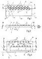
- FIG. 1 shows the one substrate part 3 of the printing chip 2, in which a plurality of recesses 7 are introduced, each having a medium chamber 11 form.
- the (100) crystal plane is parallel here to the drawing level.
- One perpendicular to the (100) crystal plane lying second crystal plane 24, for example, the (011) plane is parallel to a lateral edge 25 of the substrate part 3.
- the medium chambers 11 are seen in a top view. formed essentially rectangular. she can of course also be square.
- the recesses 7 for the medium chamber 11 are made by anisotropic etching, whereby the above-mentioned angle of 45 ° Side walls S compared to the (100) plane, as shown in Figure 2.
- the substrate part 4 In the other substrate part 4 (FIG. 3), the remaining recesses 5, 6 and 8 from the (100) crystal plane brought here.
- the substrate part 4 To the (100) plane the substrate part 4 is perpendicular to a second Crystal plane 24 ', which lie both substrate parts 3 and 4 on top of each other - an angle of 45 ° with the includes second crystal plane 24 of the substrate part 3.
- This second level 24 'could for example be the (001) crystal plane.
- the substrate part 4 is when the recesses 6 and 8 are made thus rotated by 45 ° with respect to the substrate part 4.
- connection channels 12 or feed channels 10 are in this embodiment roughly perpendicular to the second Crystal plane 24 'aligned.
- the Medium chambers 11, the feed channels 10 and the connecting channels 12 with their ejection openings 13 manufactured by anisotropic wet etching.
- the medium supply chamber 9 and this supply opening 26 are made of a different material because of their geometry ablation process, especially etching process, manufactured.
- FIGS second embodiment of a printing chip 2 closer explained. Same or equivalent Parts as described in the previous ones Figures are provided with identical reference numerals. From Figure 8 it can be seen that in the substrate part 3 the medium chambers 11 and the recesses 7 and the medium supply chamber 9 or the recess 5 introduced are. These recesses 5 and 7 are anisotropic Etching introduced into the substrate part 3.
- the longitudinal extension of the rectangular, seen in plan view Medium chambers 11 are essentially here perpendicular to the second crystal plane 24.
- Correspondingly 10 are the feed channels or Connection channels at an angle of preferably 45 ° to this second crystal plane 24 aligned so that even in this embodiment it is guaranteed that the medium chambers 11 flows through the medium essentially diagonally become.
- the connecting channel 12 sub-channels 27 and 28 comprises, which merge into one another, the one Subchannel 27 at an angle of 45 ° to the second crystal plane 24 lies and the other subchannel 28 in essentially perpendicular to this second crystal plane 24 is aligned. This will make the droplets discharged from the spray openings 13 essentially perpendicular to this second Crystal layer 24 sprayed out.
- the recesses 6 and 8 are preferably not in the substrate part 4 produced by an anisotropic etching process, so that the substrate part 4 before working it out Not 45 ° recesses from the other Substrate part 3 must be rotated.
- the Angle ä ( Figure 10) between the recesses 6 and 8 and the second level 24 as desired can be selected, with approximately 45 ° being preferred.
- the recesses 5 to 8 are introduced into the substrate parts 3 and 4 in such a way that the medium the substrate parts 3 and 4 flows alternately.
- the recesses 5 to 8 alternately in the substrate parts 3 and 4 introduced.
- the embodiment 7 are the connected ones Recesses 5 and 6 in the substrate part 4 arranged. After the medium these two recesses 5 and 6 has flowed through, it flows into the Medium chamber 11, which is in the other substrate part 3 is arranged. Then the medium flows in again the substrate part 4 through the connection channels 12 to the ejection openings 13.
- the recesses 6 to 8 and 26 can by anisotropic etching processes on the two substrate parts 3 and 4 are made, however be careful when etching and later connecting must be the corresponding substrate part 3 or 4 by 45 ° to the other Substrate part 4 or 3 is oriented so Because of the (100) crystal structure, these recesses with the second crystal level 24 respectively 24 'enclose the desired angle of 45 °. That is, the etching shadow mask for the corresponding one Substrate part 3 or 4 on the to be etched Substrate surface must be rotated by 45 ° so that due to the crystal orientation the recesses arise in the correct position. Be for the recesses 5 to 26 other etching processes applied, the orientation of the second Crystal plane 24 or 24 'not taken into account stay. The one that is specifically advantageous Etching is used for the recesses 5 to 8 and 26 chosen.
- thermal Passivated Oxide Thermal oxide is very dense, ideally adhering silicon dioxide that forms if the silicon is one at high temperatures Exposed to oxygen or water vapor atmosphere becomes.
- the printing chip 2 is provided with a heater 29 (FIG 14) assigned to at least one of the substrate parts 3 or 4 can be arranged.
- the heating device 29 especially in the area of the bottom of the recess 5 be provided so that in the supply medium chamber 9 present medium kept at temperature can be.
- the heater 29 is considered one high temperature resistant resistance heating realized, in which the resistors in particular Hafnium diboride are produced.
- the printing chip 2 at least one temperature-resistant Sensor 30 may be attached to one of the substrate parts 3 and / or 4 can be arranged.
- the temperature sensor 30 and a detection device for the output signal of the sensor is one Temperature monitoring of print chip 2 possible.
- the temperature sensor 30 can also determine the medium temperature measure, especially if he is in a very thin-walled area of the substrate parts 3 and 4 lies, these thin-walled areas, for example a bottom of a recess 5 to 8, of the hot medium.
- Pressure chip 2 for spraying hot liquid metals, in particular metal alloys and / or solders.
- low-melting ones can also be used Glasses or the like can be sprayed out.
- the printing chip 2 is suitable for the so-called Chip-size packaging (CSP) and in manufacturing a flip chip connection (FC); with these Processes are applied to solder bumps on chip substrates.
- CSP Chip-size packaging
- FC flip chip connection
- Print chip 2 is suitable.
- the printing chip 2 according to the invention is therefore versatile Production process can be used.
Landscapes
- Engineering & Computer Science (AREA)
- Mechanical Engineering (AREA)
- Particle Formation And Scattering Control In Inkjet Printers (AREA)
- Ink Jet (AREA)
- Electric Connection Of Electric Components To Printed Circuits (AREA)
Description
- Figuren 1 bis 7
- in unterschiedlichen Schnittansichten ein erstes Ausführungsbeispiel eines Druckchips,
- Figuren 8 bis 14
- in verschiedenen Schnittdarstellungen ein zweites Ausführungsbeispiel eines Druckchips, und
- Figur 15
- in schematischer Darstellung ein nach dem Tintendruckprinzip arbeitenden Druckkopf mit einem Druckchip.
Claims (21)
- Druckchip (2) für einen nach dem Tintendruckprinzip arbeitenden Druckkopf (1), mit zumindest einer eine Mediumkammer (11) bildenden Ausnehmung (7) in dem Druckchip (2), einer eine Wandung der Mediumkammer (11) bildenden auslenkbaren Membran (14), einem in der Mediumkammer (11) mündenden Kanal (10) für die Zuführung eines heiß auszuspritzenden, flüssigen Mediums, und mit einer mit der Mediumkammer (11) verbundenen Ausspritzöffnung (13), wobei der Druckchip (2) ausschließlich aus einkristallinem Silizium hergestellt und aus zumindest zwei aufeinanderliegenden Substratteilen (3,4) gebildet ist, dadurch gekennzeichnet, dass der Zuführkanal (10) und ein die Ausspritzöffnung (13) der Mediumkammer (11) verbindender Verbindungskanal (12) um 45° gegenüber einer senkrecht zur (100)-Kristallebene des Siliziumkristalls liegenden zweiten Kristallebene (24,24') verlaufen und dass die Mediumkammer (11) einen Winkel von 45° mit der senkrecht zur (100)-Kristallebene liegenden zweiten Kristallebene (24,24') einschließt und der Zuführkanal (10) und der Verbindungskanal (12) senkrecht zu dieser zweiten Kristallebene (24) liegen, und dass die jeweilige Kristallebene der aneinanderliegenden Oberflächen der aufeinanderliegenden Substratteile (3,4) jeweils der (100)-Kristallebene entsprechen.
- Druckchip nach Anspruch 1, dadurch gekennzeichnet, dass der Zuführkanal (10), die Mediumkammer (11) und die Ausspritzöffnung (13) so in dem Druckchip (2) angeordnet sind, dass das Medium abwechselnd durch die Substratteile (3,4) fließt.
- Druckchip nach einem der vorhergehenden Ansprüche, dadurch gekennzeichnet, dass in dem Druckchip (2) eine Mediumversorgungskammer (9) liegt, mit der der Zuführkanal (10) verbunden ist.
- Druckchip nach einem der vorhergehenden Ansprüche, dadurch gekennzeichnet, dass die Druckchipoberflächen, insbesondere die mit dem heißen Medium in Berührung kommenden, mit einer hochtemperaturbeständigen Beschichtung versehen sind.
- Druckchip nach einem der vorhergehenden Ansprüche, dadurch gekennzeichnet, dass die Druckchipoberflächen, insbesondere die mit dem heißen Medium in Berührung kommenden, durch thermisches Oxid passiviert sind.
- Druckchip nach einem der vorhergehenden Ansprüche, dadurch gekennzeichnet, dass die Substratteile (3,4) durch Silicon-Fusion-Bonding untrennbar miteinander verbunden sind.
- Druckchip nach einem der vorhergehenden Ansprüche, dadurch gekennzeichnet, dass die Ausnehmung (7) für die Mediumkammer (11), der Zuführkanal (10), die Ausspritzöffnung (13) und die Mediumversorgungskammer (9) durch ein anisotropes Nass- oder Trockenätzverfahren hergestellt sind.
- Druckchip nach einem der vorhergehenden Ansprüche, dadurch gekennzeichnet, dass die Mediumkammer (11), der Zuführkanal (10) und die Ausspritzöffnung (13) -in Flussrichtung des Mediums gesehen- einen trapezförmigen oder V-förmigen Querschnitt besitzen.
- Druckchip nach einem der vorhergehenden Ansprüche, dadurch gekennzeichnet, dass die Mediumkammer (11) in Draufsicht rechteckig ausgebildet ist und dass der Zuführkanal (10) so in der Mediumkammer (11) mündet und die Ausspritzöffnung (13) so mit der Mediumkammer (11) verbunden ist, dass diese im Wesentlichen diagonal von dem Medium durchströmt wird.
- Druckchip nach einem der vorhergehenden Ansprüche, dadurch gekennzeichnet, dass die Mediumkammer (11), der Zuführkanal (10), die Ausspritzöffnung (13) und die Mediumversorgungskammer (9) von der (100)-Kristallebene des Siliziumkristalls eingebracht sind.
- Druckchip nach einem der vorhergehenden Ansprüche, dadurch gekennzeichnet, dass der Boden (15) der Ausnehmung (7) die Membran (14) bildet.
- Druckchip nach einem der vorhergehenden Ansprüche, dadurch gekennzeichnet, dass der Verbindungskanal (12) zumindest einen senkrecht zur zweiten Kristallebene (24) liegenden Teilkanal (28) aufweist, dessen Mündung am Rand (25) des Druckchips (2) die Ausspritzöffnung (13) bildet.
- Druckchip nach einem der vorhergehenden Ansprüche, dadurch gekennzeichnet, dass der Zuführkanal (10) eine Drosselstelle (17) aufweist oder als Drossel ausgebildet ist.
- Druckchip nach einem der vorhergehenden Ansprüche, dadurch gekennzeichnet, dass in einem der Substratteile (3,4) die Mediumkammer (11) und die Versorgungskammer (9) liegen, die gegeneinander durch einen Steg (16) begrenzt sind, und dass der Zuführkanal (10) in dem anderen der Substratteile (3,4) ausgebildet ist und unter dem freien Ende des Steges (16) liegt.
- Druckchip nach einem der vorhergehenden Ansprüche, gekennzeichnet durch mehrere Mediumkammern (11), Zuführkanäle (10), Verbindungskanäle (12) und Ausspritzöffnungen (13).
- Druckchip nach einem der vorhergehenden Ansprüche, gekennzeichnet durch zumindest ein Heizelement (29), das an der Außenseite zumindest eines der Substatteile (3,4) liegt.
- Druckchip nach einem der vorhergehenden Ansprüche, gekennzeichnet durch zumindest einen an der Außenseite an zumindest einem der Substratteile (3,4) liegenden Temperatursensor (30).
- Druckchip nach einem der vorhergehenden Ansprüche, dadurch gekennzeichnet, dass die Membran (14) eine Dicke von zirka 20 bis 100 µm aufweist.
- Druckchip nach Anspruch 7, dadurch gekennzeichnet, dass -wenn die Ausnehmungen (5 bis 8,26) in beiden Substratteilen (3,4) durch anisotropes Ätzen eingebracht sind- die beiden Substratteile (3,4) beim Ätzen und beim späteren Verbinden, bezogen auf die senkrecht zur (100)-Substratoberfläche liegenden (100)-Kristallebenen, um 45° zueinander verdreht sind.
- Verwendung eines Druckchips nach einem der Ansprüche 1 bis 19 zum Ausspritzen von bis über 1000°C heißen, flüssigen Medien.
- Druckkopf, der nach dem Tintendruckprinzip arbeitet, gekennzeichnet durch einen Druckchip nach einem der Ansprüche 1 bis 19.
Applications Claiming Priority (3)
| Application Number | Priority Date | Filing Date | Title |
|---|---|---|---|
| DE19931110 | 1999-07-06 | ||
| DE19931110A DE19931110A1 (de) | 1999-07-06 | 1999-07-06 | Druckkopf zum Ausspritzen eines heißen flüssigen Mediums und Verfahren zur Herstellung einer metallisches Lot umfassenden Verbindungsstelle |
| PCT/EP2000/006405 WO2001002122A1 (de) | 1999-07-06 | 2000-07-06 | Druckchip für einen nach dem tintendruckprinzip arbeitenden druckkopf |
Publications (2)
| Publication Number | Publication Date |
|---|---|
| EP1200223A1 EP1200223A1 (de) | 2002-05-02 |
| EP1200223B1 true EP1200223B1 (de) | 2004-11-03 |
Family
ID=7913784
Family Applications (2)
| Application Number | Title | Priority Date | Filing Date |
|---|---|---|---|
| EP00949274A Expired - Lifetime EP1200223B1 (de) | 1999-07-06 | 2000-07-06 | Druckchip für einen nach dem tintendruckprinzip arbeitenden druckkopf |
| EP00949275A Expired - Lifetime EP1200224B1 (de) | 1999-07-06 | 2000-07-06 | Druckkopf zum ausspritzen eines heissen flüssigen mediums |
Family Applications After (1)
| Application Number | Title | Priority Date | Filing Date |
|---|---|---|---|
| EP00949275A Expired - Lifetime EP1200224B1 (de) | 1999-07-06 | 2000-07-06 | Druckkopf zum ausspritzen eines heissen flüssigen mediums |
Country Status (10)
| Country | Link |
|---|---|
| US (1) | US6773084B1 (de) |
| EP (2) | EP1200223B1 (de) |
| JP (2) | JP2003525768A (de) |
| KR (2) | KR20020035829A (de) |
| CN (2) | CN1173792C (de) |
| AU (2) | AU6269300A (de) |
| DE (3) | DE19931110A1 (de) |
| IL (2) | IL147466A0 (de) |
| TW (1) | TW501981B (de) |
| WO (2) | WO2001002123A1 (de) |
Families Citing this family (15)
| Publication number | Priority date | Publication date | Assignee | Title |
|---|---|---|---|---|
| KR100482697B1 (ko) * | 2001-11-15 | 2005-04-13 | 주식회사 프리텍 | 압전소자를 이용한 디스펜서 |
| DE10317872A1 (de) | 2002-04-18 | 2004-01-08 | Hitachi Printing Solutions, Ltd., Ebina | Tintenstrahlkopf und Verfahren zu seiner Herstellung |
| USD514618S1 (en) * | 2002-09-12 | 2006-02-07 | Seiko Epson Corporation | Ink jet liquid injector |
| DE10242818B4 (de) * | 2002-09-14 | 2004-07-29 | Fachhochschule Heilbronn - Hochschule für Technik und Wirtschaft | Druckkopf zum Ausspritzen eines heissen flüssigen Mediums |
| DE10332760B3 (de) * | 2003-07-17 | 2005-02-17 | Fachhochschule Heilbronn Hochschule für Wirtschaft und Technik | Fluidausgabevorrichtung |
| US7917941B2 (en) | 2003-09-22 | 2011-03-29 | International Business Machines Corporation | System and method for providing physical web security using IP addresses |
| DE102005018274A1 (de) * | 2005-04-14 | 2006-10-19 | Würth Elektronik Schopfheim GmbH & Co. KG | Verfahren zum Herstellen einer Leiterplatte |
| JP2008085247A (ja) * | 2006-09-29 | 2008-04-10 | Omron Corp | 半田付け装置および該半田付け装置を用いた半田付け方法 |
| DE102006051607B4 (de) * | 2006-11-02 | 2008-11-20 | Mühlbauer Ag | Verfahren und Vorrichtung zum serienmäßigen Aufbringen und Befestigen von elektronischen Bauteilen auf Substraten |
| JP5382938B2 (ja) | 2007-02-20 | 2014-01-08 | コヴィディエン リミテッド パートナーシップ | 環状穿刺器を有する手術器具 |
| JP4957452B2 (ja) * | 2007-08-22 | 2012-06-20 | ブラザー工業株式会社 | 液体移送装置 |
| CN101801671B (zh) * | 2008-03-26 | 2013-08-07 | 日本碍子株式会社 | 液滴吐出装置及液滴吐出装置的制造方法 |
| US8911463B2 (en) | 2008-06-10 | 2014-12-16 | Covidien Lp | Bladed/bladeless obturator for use in a surgical trocar assembly |
| DE102012106942A1 (de) * | 2012-07-30 | 2014-01-30 | Endress + Hauser Flowtec Ag | Verfahren zum Austauschen mindestens einer auf einem Träger angeordneten elektronischen Komponente |
| DE102014102597A1 (de) * | 2014-02-27 | 2015-08-27 | Endress + Hauser Gmbh + Co. Kg | Verfahren zum Variieren des Abstands zwischen einem Leiterplattenanschluss und einem Bauteilanschluss |
Family Cites Families (22)
| Publication number | Priority date | Publication date | Assignee | Title |
|---|---|---|---|---|
| DE3047884A1 (de) * | 1980-12-18 | 1982-07-15 | Siemens AG, 1000 Berlin und 8000 München | Vorrichtung zur automatisierbaren bearbeitung in der halbleitertechnologie, z.b. von leiterplatten |
| US4835554A (en) | 1987-09-09 | 1989-05-30 | Spectra, Inc. | Ink jet array |
| DE3804165A1 (de) * | 1988-02-11 | 1989-08-24 | Olympia Aeg | Verfahren zum bestuecken eines tintenstrahldruckkopfes mit piezokristallen |
| DE3805841A1 (de) * | 1988-02-22 | 1989-08-31 | Siemens Ag | Verfahren zum bestuecken von bauelementetraegern mit bauelementen in oberflaechenmontagetechnik |
| US4935752A (en) * | 1989-03-30 | 1990-06-19 | Xerox Corporation | Thermal ink jet device with improved heating elements |
| SG83626A1 (en) * | 1989-07-11 | 2001-10-16 | Seiko Epson Corp | Piezoelectric/electrostrictive actuator having at least one piezoelectric/electrostrictive film |
| US5010355A (en) * | 1989-12-26 | 1991-04-23 | Xerox Corporation | Ink jet printhead having ionic passivation of electrical circuitry |
| GB2297726B (en) * | 1993-05-04 | 1997-02-19 | Markem Corp | Ink jet printing system |
| EP0637057B1 (de) * | 1993-07-30 | 1996-12-11 | International Business Machines Corporation | Vorrichtung und Verfahren um feine Metal-linie auf einem Substrat abzulegen |
| DE69506306T2 (de) | 1994-04-20 | 1999-06-10 | Seiko Epson Corp., Tokio/Tokyo | Tintenstrahlaufzeichungsgerät und Verfahren zur Herstellung eines Tintenstrahlkopfes |
| US5560543A (en) | 1994-09-19 | 1996-10-01 | Board Of Regents, The University Of Texas System | Heat-resistant broad-bandwidth liquid droplet generators |
| JPH0890769A (ja) * | 1994-09-27 | 1996-04-09 | Sharp Corp | ひだ付きダイアフラム型インクジェットヘッド |
| DE4443254C1 (de) * | 1994-11-25 | 1995-12-21 | Francotyp Postalia Gmbh | Anordnung für einen Tintendruckkopf aus einzelnen Tintendruckmodulen |
| US5772106A (en) * | 1995-12-29 | 1998-06-30 | Microfab Technologies, Inc. | Printhead for liquid metals and method of use |
| WO1997034769A1 (en) * | 1996-03-18 | 1997-09-25 | Seiko Epson Corporation | Ink jet head and method of manufacturing same |
| US6220698B1 (en) * | 1996-07-26 | 2001-04-24 | Seiko Epson Corporation | Ink jet type recording head |
| JPH1095113A (ja) * | 1996-09-24 | 1998-04-14 | Seiko Epson Corp | インクジェット式記録ヘッド |
| US5876615A (en) * | 1997-01-02 | 1999-03-02 | Hewlett-Packard Company | Molten solder drop ejector |
| JPH11992A (ja) * | 1997-04-17 | 1999-01-06 | Ricoh Co Ltd | インクジェットヘッド |
| JPH10315461A (ja) * | 1997-05-14 | 1998-12-02 | Seiko Epson Corp | インクジェットヘッドおよびその製造方法 |
| US6019907A (en) | 1997-08-08 | 2000-02-01 | Hewlett-Packard Company | Forming refill for monolithic inkjet printhead |
| US5980025A (en) * | 1997-11-21 | 1999-11-09 | Xerox Corporation | Thermal inkjet printhead with increased resistance control and method for making the printhead |
-
1999
- 1999-07-06 DE DE19931110A patent/DE19931110A1/de not_active Ceased
-
2000
- 2000-07-06 WO PCT/EP2000/006407 patent/WO2001002123A1/de not_active Ceased
- 2000-07-06 KR KR1020027000141A patent/KR20020035829A/ko not_active Ceased
- 2000-07-06 KR KR1020027000142A patent/KR20020035830A/ko not_active Ceased
- 2000-07-06 WO PCT/EP2000/006405 patent/WO2001002122A1/de not_active Ceased
- 2000-07-06 IL IL14746600A patent/IL147466A0/xx unknown
- 2000-07-06 AU AU62693/00A patent/AU6269300A/en not_active Abandoned
- 2000-07-06 JP JP2001507599A patent/JP2003525768A/ja active Pending
- 2000-07-06 EP EP00949274A patent/EP1200223B1/de not_active Expired - Lifetime
- 2000-07-06 JP JP2001507600A patent/JP2003524882A/ja active Pending
- 2000-07-06 CN CNB008099448A patent/CN1173792C/zh not_active Expired - Fee Related
- 2000-07-06 CN CN00809943A patent/CN1360530A/zh active Pending
- 2000-07-06 US US10/030,069 patent/US6773084B1/en not_active Expired - Fee Related
- 2000-07-06 EP EP00949275A patent/EP1200224B1/de not_active Expired - Lifetime
- 2000-07-06 AU AU62694/00A patent/AU6269400A/en not_active Abandoned
- 2000-07-06 IL IL14746500A patent/IL147465A0/xx unknown
- 2000-07-06 DE DE50008768T patent/DE50008768D1/de not_active Expired - Lifetime
- 2000-07-06 DE DE50008518T patent/DE50008518D1/de not_active Expired - Fee Related
- 2000-07-31 TW TW089113632A patent/TW501981B/zh not_active IP Right Cessation
Also Published As
| Publication number | Publication date |
|---|---|
| AU6269400A (en) | 2001-01-22 |
| EP1200224A1 (de) | 2002-05-02 |
| CN1173792C (zh) | 2004-11-03 |
| DE19931110A1 (de) | 2001-01-25 |
| CN1360531A (zh) | 2002-07-24 |
| JP2003525768A (ja) | 2003-09-02 |
| EP1200223A1 (de) | 2002-05-02 |
| US6773084B1 (en) | 2004-08-10 |
| JP2003524882A (ja) | 2003-08-19 |
| EP1200224B1 (de) | 2004-11-24 |
| DE50008518D1 (de) | 2004-12-09 |
| IL147466A0 (en) | 2002-08-14 |
| TW501981B (en) | 2002-09-11 |
| IL147465A0 (en) | 2002-08-14 |
| CN1360530A (zh) | 2002-07-24 |
| WO2001002122A1 (de) | 2001-01-11 |
| KR20020035830A (ko) | 2002-05-15 |
| KR20020035829A (ko) | 2002-05-15 |
| AU6269300A (en) | 2001-01-22 |
| DE50008768D1 (de) | 2004-12-30 |
| WO2001002123A1 (de) | 2001-01-11 |
Similar Documents
| Publication | Publication Date | Title |
|---|---|---|
| DE60113798T2 (de) | Integrierter cmos/mems-tintenstrahldruckknopf mit lang gestrecktem düsenloch und verfahren zu dessen herstellung | |
| DE69305477T2 (de) | Antriebselement mit keramischem Substrat und Tintenstrahldruckkopf mit Benützung derselben | |
| DE60115592T2 (de) | Integrierter CMOS/MEMS Tintenstrahldruckkopf mit während der CMOS-Bearbeitung ausgebildeten Heizelementen und Verfahren zum Ausbilden derselben | |
| DE69509986T2 (de) | Vereinfachter tintenstrahldruckkopf | |
| DE69823783T2 (de) | Verfahren zum herstellen von tintenstrahl-aufzeichnungsköpfen | |
| DE69129159T2 (de) | Tintenstrahlkopf | |
| DE60111716T2 (de) | Integrierter cmos/mems-tintenstrahldruckkopf mit seitenstromdrüsen-architektur auf oxidbasis und verfahren zu dessen herstellung | |
| DE69624012T2 (de) | Aufzeichnungskopf des Tintenstrahltypes | |
| DE60117220T2 (de) | Tintenstrahldruckkopf mit kapillarer strömungsreinigung | |
| DE69934469T2 (de) | Druckköpfe | |
| EP1200223A1 (de) | Druckchip für einen nach dem tintendruckprinzip arbeitenden druckkopf | |
| DE4214555A1 (de) | Anordnung für einen elektrothermischen Tintendruckkopf | |
| DE102011005471A1 (de) | Mikro-Ejektor und Verfahren für dessen Herstellung | |
| DE19626822B4 (de) | Tintenstrahlkopf und Herstellungsverfahren einer Düsenplatte | |
| DE69104072T2 (de) | Thermische Tintenstrahldruckköpfe. | |
| DE60207621T2 (de) | Tintenstrahlaufzeichnungskopf und Tintenstrahlaufzeichnungsapparat | |
| DE4025619C2 (de) | Druckelement für einen Druckkopf für das Tintenspritz-Verfahren nach dem Bubble-Jet-Prinzip | |
| EP0150348A2 (de) | Schreibkopf für Tintenschreibeinrichtungen | |
| DE60109880T2 (de) | Einbau von Zusatzheizeinrichtungen in die Tintenkanäle eines integrierten CMOS/MEMS-Tintenstrahldruckkopfs und Verfahren zum Ausbilden desselben | |
| DE69518672T2 (de) | Tintenstrahldrucken | |
| DE102005019184B4 (de) | Verfahren zum Erzeugen eines Druckkopfs | |
| DE69616656T2 (de) | Aufzeichnungskopf nach der Tintenstrahlart | |
| DE19813470B4 (de) | Tintenstrahldruckkopf | |
| DE69710411T2 (de) | Tintenstrahldruckkopf und Verfahren zu seiner Herstellung | |
| EP0852539B1 (de) | Tintenstrahldruckkopf und verfahren zum herstellen eines solchen tintenstrahldruckkopfes |
Legal Events
| Date | Code | Title | Description |
|---|---|---|---|
| PUAI | Public reference made under article 153(3) epc to a published international application that has entered the european phase |
Free format text: ORIGINAL CODE: 0009012 |
|
| 17P | Request for examination filed |
Effective date: 20020206 |
|
| AK | Designated contracting states |
Kind code of ref document: A1 Designated state(s): AT BE CH CY DE DK ES FI FR GB GR IE IT LI LU MC NL PT SE |
|
| AX | Request for extension of the european patent |
Free format text: AL;LT;LV;MK;RO;SI |
|
| 17Q | First examination report despatched |
Effective date: 20031103 |
|
| GRAP | Despatch of communication of intention to grant a patent |
Free format text: ORIGINAL CODE: EPIDOSNIGR1 |
|
| RBV | Designated contracting states (corrected) |
Designated state(s): DE GB |
|
| GRAS | Grant fee paid |
Free format text: ORIGINAL CODE: EPIDOSNIGR3 |
|
| GRAA | (expected) grant |
Free format text: ORIGINAL CODE: 0009210 |
|
| AK | Designated contracting states |
Kind code of ref document: B1 Designated state(s): DE GB |
|
| REG | Reference to a national code |
Ref country code: GB Ref legal event code: FG4D Free format text: NOT ENGLISH |
|
| REF | Corresponds to: |
Ref document number: 50008518 Country of ref document: DE Date of ref document: 20041209 Kind code of ref document: P |
|
| REG | Reference to a national code |
Ref country code: IE Ref legal event code: FG4D Free format text: GERMAN |
|
| GBT | Gb: translation of ep patent filed (gb section 77(6)(a)/1977) |
Effective date: 20050203 |
|
| PGFP | Annual fee paid to national office [announced via postgrant information from national office to epo] |
Ref country code: GB Payment date: 20050615 Year of fee payment: 6 |
|
| REG | Reference to a national code |
Ref country code: IE Ref legal event code: FD4D |
|
| PGFP | Annual fee paid to national office [announced via postgrant information from national office to epo] |
Ref country code: DE Payment date: 20050729 Year of fee payment: 6 |
|
| PLBE | No opposition filed within time limit |
Free format text: ORIGINAL CODE: 0009261 |
|
| STAA | Information on the status of an ep patent application or granted ep patent |
Free format text: STATUS: NO OPPOSITION FILED WITHIN TIME LIMIT |
|
| 26N | No opposition filed |
Effective date: 20050804 |
|
| PG25 | Lapsed in a contracting state [announced via postgrant information from national office to epo] |
Ref country code: GB Free format text: LAPSE BECAUSE OF NON-PAYMENT OF DUE FEES Effective date: 20060706 |
|
| PG25 | Lapsed in a contracting state [announced via postgrant information from national office to epo] |
Ref country code: DE Free format text: LAPSE BECAUSE OF NON-PAYMENT OF DUE FEES Effective date: 20070201 |
|
| GBPC | Gb: european patent ceased through non-payment of renewal fee |
Effective date: 20060706 |