EP1197784A1 - Elektrooptische vorrichtung und deren herstellungsverfahren - Google Patents
Elektrooptische vorrichtung und deren herstellungsverfahren Download PDFInfo
- Publication number
- EP1197784A1 EP1197784A1 EP00939142A EP00939142A EP1197784A1 EP 1197784 A1 EP1197784 A1 EP 1197784A1 EP 00939142 A EP00939142 A EP 00939142A EP 00939142 A EP00939142 A EP 00939142A EP 1197784 A1 EP1197784 A1 EP 1197784A1
- Authority
- EP
- European Patent Office
- Prior art keywords
- buffer layer
- protective film
- electro
- optical waveguide
- electrodes
- Prior art date
- Legal status (The legal status is an assumption and is not a legal conclusion. Google has not performed a legal analysis and makes no representation as to the accuracy of the status listed.)
- Withdrawn
Links
Images





Classifications
-
- G—PHYSICS
- G02—OPTICS
- G02F—OPTICAL DEVICES OR ARRANGEMENTS FOR THE CONTROL OF LIGHT BY MODIFICATION OF THE OPTICAL PROPERTIES OF THE MEDIA OF THE ELEMENTS INVOLVED THEREIN; NON-LINEAR OPTICS; FREQUENCY-CHANGING OF LIGHT; OPTICAL LOGIC ELEMENTS; OPTICAL ANALOGUE/DIGITAL CONVERTERS
- G02F1/00—Devices or arrangements for the control of the intensity, colour, phase, polarisation or direction of light arriving from an independent light source, e.g. switching, gating or modulating; Non-linear optics
- G02F1/01—Devices or arrangements for the control of the intensity, colour, phase, polarisation or direction of light arriving from an independent light source, e.g. switching, gating or modulating; Non-linear optics for the control of the intensity, phase, polarisation or colour
- G02F1/03—Devices or arrangements for the control of the intensity, colour, phase, polarisation or direction of light arriving from an independent light source, e.g. switching, gating or modulating; Non-linear optics for the control of the intensity, phase, polarisation or colour based on ceramics or electro-optical crystals, e.g. exhibiting Pockels effect or Kerr effect
- G02F1/035—Devices or arrangements for the control of the intensity, colour, phase, polarisation or direction of light arriving from an independent light source, e.g. switching, gating or modulating; Non-linear optics for the control of the intensity, phase, polarisation or colour based on ceramics or electro-optical crystals, e.g. exhibiting Pockels effect or Kerr effect in an optical waveguide structure
-
- G—PHYSICS
- G02—OPTICS
- G02F—OPTICAL DEVICES OR ARRANGEMENTS FOR THE CONTROL OF LIGHT BY MODIFICATION OF THE OPTICAL PROPERTIES OF THE MEDIA OF THE ELEMENTS INVOLVED THEREIN; NON-LINEAR OPTICS; FREQUENCY-CHANGING OF LIGHT; OPTICAL LOGIC ELEMENTS; OPTICAL ANALOGUE/DIGITAL CONVERTERS
- G02F2201/00—Constructional arrangements not provided for in groups G02F1/00 - G02F7/00
- G02F2201/07—Constructional arrangements not provided for in groups G02F1/00 - G02F7/00 buffer layer
-
- G—PHYSICS
- G02—OPTICS
- G02F—OPTICAL DEVICES OR ARRANGEMENTS FOR THE CONTROL OF LIGHT BY MODIFICATION OF THE OPTICAL PROPERTIES OF THE MEDIA OF THE ELEMENTS INVOLVED THEREIN; NON-LINEAR OPTICS; FREQUENCY-CHANGING OF LIGHT; OPTICAL LOGIC ELEMENTS; OPTICAL ANALOGUE/DIGITAL CONVERTERS
- G02F2201/00—Constructional arrangements not provided for in groups G02F1/00 - G02F7/00
- G02F2201/50—Protective arrangements
Definitions
- the present invention relates to an electro-optic element and manufacturing method therefor.
- the present invention relates to an electro-optic element which can be suitably used in optical waveguide modulators for optical communications or optical measurement, and to a manufacturing method therefore.
- FIG. 7 is a cross-section showing an example of a conventional optical waveguide modulator.
- This optical waveguide modulator comprises a ferroelectric substrate made of lithium niobate (LiNbO 3 ) which is most generally and practically used in ferroelectric substrates for optical waveguide modulators.
- reference 10 indicates a ferroelectric substrate comprising an X-cut lithium niobate.
- this ferroelectric substrate 10 is cut along the X-axis direction (the crystallographic c-axis), which forms the principal optical axis
- the Z-cut ferroelectric substrate 10 exhibits the pyroelectric effect (electric-optic effect).
- the axis which exhibits the pyroelectric effect (electric-optic effect) of this ferroelectric substrate 10 is the Z-axis direction (the crystallographic c-axis) which forms the principal optical axis, and as shown in FIG. 7, it is a direction which is parallel to the face (in this specification this is referred to as the "main face") of the ferroelectric substrate 10 in which optical wave guides 2 and 2 are formed.
- the optical waveguides 2 and 2 in which Ti has been thermally diffused are formed.
- a buffer layer 3 comprising SiO 2 is formed.
- electrodes 4 comprising Au are formed so that they lie parallel to the optical wave guides 2 and 2.
- a transition metal layer 5 comprising a transition metal such as Ti, Cr, or Ni is provided between these electrodes 4 and the buffer layer 3.
- optical waveguide modulator a method is used in which, first, optical waveguides 2 and 2 are formed in the main face of the ferroelectric substrate 10 by a thermal diffusion method. And the buffer layer 3 is formed by means of a vacuum deposition method, a sputtering method, or the like on the side of ferroelectric substrate 10 in which the optical waveguides 2 and 2 are formed. Next, a transition metal film and an Au film are successively formed across the entire surface of the buffer layer 3 by means of a vacuum deposition method. In addition, electrodes 4 are formed on this Au film by using an electrolytic plating method onto only the electrode formation regions which are regions on which the electrodes 4 and 4 are formed. Thereafter, the Au film and the transition metal film which remain between the electrodes 4 and 4 are removed by chemical etching, and the transition metal layer 5 is completed.
- the direction of the Z-axis of the ferroelectric substrate 10 is parallel to the main face of the ferroelectric substrate 10.
- the direction of the Z-axis of the ferroelectric substrate 11 is orthogonal to the main face of the ferroelectric substrate 11.
- the generation of an electric charge due to the pyroelectric effect between the electrodes 4 and 4 is tend to occur. If the charge due to the pyroelectric effect accumulates between the electrodes 4 and 4, due to a random discharge phenomenon, or the like, the interaction between the electrodes 4 and 4 and the optical waveguides 2 and 2 becomes disturbed, and the modulation conditions of signals of the optical waveguide modulator become noticeably unstable.
- the charge which is generated by the pyroelectric effect does not substantially accumulate between the electrodes 4 and 4, and it has the advantage that problems due to the pyroelectric effect do not occur.
- the buffer layer 3 is exposed between the electrodes 4 and 4. Therefore, there is the problem that the surface 3a at which the buffer layer 3 is exposed and the inner part of buffer layer 3 are easily contaminated by contaminants such as K, Ti, and Cr.
- dc drift is a phenomenon in which the electric current being applied to the electrodes 4 and 4 leaks through the buffer layer 3 due to the presence of mobile ions such as alkali ions, such as K and Na, and protons, the desired voltage is not applied effectively on the device, and this has a negative impact on the properties of the optical waveguide modulator.
- the contaminants of the buffer layer 3 reach the interface with the ferroelectric substrate 10 due to thermal treatments in the mounting process and the like, due to the contaminants, the chemical bonds of the buffer layer 3 comprising SiO 2 are broken, the bonds which bond the ferroelectric substrate 10 comprising lithium niobate and the buffer layer 3 are reduced, and the problem results that the bonding strength between the two is remarkably weakened.
- this optical waveguide modulator uses a ferroelectric substrate comprising lithium niobate (LiNbO 3 ), however, the direction of the Z-axis which exhibits the pyroelectric effect of the ferroelectric substrate is different to that of the optical waveguide modulator shown in FIG. 7.
- reference 11 indicates a ferroelectric substrate comprising lithium niobate having a Z-cut.
- the direction of the Z-axis which exhibits the pyroelectric effect of this ferroelectric substrate 11 is orthogonal to the main face of the ferroelectric substrate 11 in which the optical wave guides 2 and 2 are formed.
- optical waveguides 2 and 2 comprising Ti are formed, and above that, a buffer layer 3 comprising SiO 2 is formed.
- a semi-conductive film 6 comprising an Si thin film or the like is provided onto the buffer layer 3.
- electrodes 4 comprising Au are formed so that they lie parallel to the optical waveguides 2 and 2.
- the direction of the Z-axis of the ferroelectric substrate 11 is orthogonal to the main face of the ferroelectric substrate 11. Therefore, when the surrounding temperature changes, an electric charge is readily generated due to the pyroelectric effect between the electrodes 4 and 4. If the charge due to the pyroelectric effect accumulates between the electrodes 4 and 4, due to a random discharge phenomenon, or the like, the interaction between the electrodes 4 and 4 and the optical waveguides 2 and 2 becomes disordered, and the modulation conditions of signals of the optical waveguide modulator become noticeably unstable.
- a semi-conductive film 6 is provided on the buffer layer 3.
- This semi-conductive film 6 responds to the linear electric field induced by the pyroelectric effect, and it makes the charge due to the pyroelectric effect diffuse uniformly over the whole of the semi-conductive film 6. By doing this, even when a pyroelectric effect is generated, the random discharge phenomenon can be suppressed, and it is possible to stabilize the modulation conditions of the signals of the optical waveguide modulator.
- the optical waveguide modulator shown in FIG. 9 differs from the optical waveguide modulator shown in FIG. 8 in that the semi-conductive film 61 is divided by portions on whose upper surfaces electrodes 4 and 4 are not formed.
- the present invention aims to solve the above-mentioned problems and has an object of providing an electro-optic element in which the accumulation of charge generated due to the pyroelectric effect is less likely to occur, and in which contamination of the surface of the buffer layer and the inner portion of the buffer layer is less likely to occur.
- the present invention has an object of providing a manufacturing method for the above-mentioned electro-optic element.
- the electro-optic element of the present invention comprises a ferroelectric substrate comprising a single crystal having an electro-optic effect, in which an optical waveguide is formed by thermal diffusion of titanium in the main face, and in which an axis in which the above-mentioned electro-optic effect is induced is in a direction parallel to the above-mentioned main face; a heat treated buffer layer provided on the above-mentioned ferroelectric substrate on a side in which the above-mentioned optical waveguides are formed; electrodes provided on a part of the above-mentioned buffer layer; and a protective film for preventing the contamination of the buffer layer, which is provided on at least the region of the buffer layer on which the electrodes are not formed.
- main face means the face of the ferroelectric substrate, in which the optical waveguides are formed.
- the structure of the electro-optic element of the present invention is basically such that the axis in which the electro-optic effect of the ferroelectric substrate is induced is parallel to the main face of the ferroelectric substrate. This corresponds to the example of a conventional optical waveguide modulator shown in FIG. 7.
- the electro-optic element of the present invention since the axis in which the electro-optic effect of the ferroelectric substrate is induced is parallel to the main face of the above-mentioned ferroelectric substrate, the charge which is generated by the electro-optic effect is essentially not stored between the electrodes, and problems resulting from the pyroelectric effect do not occur.
- the electro-optic element of the present invention since a protective film is provided on at least the region of the above-mentioned buffer layer on which the above-mentioned electrodes are not formed, the surface of the buffer layer is not exposed. For this reason, the electro-optic element is such that it is difficult for the surface of the buffer layer and inner portion of the buffer layer to be contaminated.
- the above-mentioned protective film is provided over an entire surface of the above-mentioned buffer layer including regions on which the above-mentioned electrodes are formed.
- the whole surface of the buffer layer is covered by the protective film, and it is possible to prevent contamination of the buffer layer during the manufacturing process of the electro-optic element after the protective film has been formed, and it is possible to prevent even further penetration of contaminants into the buffer layer.
- the protective film is formed on the entire surface of the buffer layer, it is easier to form the protective film compared with a situation in which the protective film is formed on a part of the surface of the buffer layer.
- said protective film it is preferable for said protective film to be also provided on the side surfaces of said buffer layer with respect to the optical waveguide direction.
- the side surfaces of the above-mentioned buffer layer with respect to the direction of the optical waveguides are covered by the protective film, and therefore, it is possible to prevent even more the penetration of contaminants into the buffer layer.
- the above-mentioned protective film provided on the top of said buffer layer and the protective film provided on the side surfaces of said buffer layer with respect to the optical waveguide direction prefferably be made of the same material.
- this type of electro-optic element By means of making this type of electro-optic element, it is possible to increase the chemical bonding strength of the protective film provided on the buffer layer and the protective film provided on the side surfaces of the buffer layer with respect to the optical waveguide direction. Furthermore, since the thermal expansion properties of the protective film provided on the top of the buffer layer and the protective film provided on the sides of the buffer layer are the same, the adhesiveness at the interface between the protective film provided on the top of the buffer layer and the protective film provided on the side surfaces of the buffer layer is thermally stable. As a result, it is possible to improve the effect of the protective film in preventing penetration of contaminants into the buffer layer, and it is possible to obtain even greater stability.
- the above-mentioned protective film it is preferable for the above-mentioned protective film to be an amorphous film.
- an amorphous film Compared with a crystalline film, an amorphous film has structural continuity, and is dense. For this reason, by making the protective film an amorphous film, it is possible to form an electro-optic element in which it is even more difficult for the surface of the buffer layer and the inside of the buffer layer to be contaminated.
- the above-mentioned protective film it is preferable for the above-mentioned protective film to be electrically insulative.
- electrically insulative means a direct current resistance of greater than 20 M Q and preferably greater than 50 M ⁇ .
- the protective film comprises at least one type selected from the group consisting of silicon (Si), silicon carbide (Si-C), and silicon nitride (Si-N).
- the protective film comprises at least one type selected from the group consisting of silicon (Si), silicon carbide (Si-C), and silicon nitride (Si-N) which contain Si and which have high covalency, absorption of moisture is less likely to occur compared with SiO 2 .
- the buffer layer comprises SiO 2
- the operation of the protective film in preventing the penetration of contaminants into the buffer layer is even better, and it is even more difficult for contamination of the buffer layer to occur.
- the protective film comprising at least one selected from the group consisting of silicon (Si), silicon carbide (Si-C), and silicon nitride (Si-N) does not contain oxygen, even when a transition metal layer is formed from a chemically active transition metal such as Ti on the protective film, there is no oxidative degradation of the transition metal layer and it is possible to obtain a stable film bonding strength.
- the above-mentioned ferroelectric substrate of the electro-optic element comprises lithium niobate.
- the manufacturing method for electro-optic elements of the present invention comprises a step of forming optical waveguides in a surface of a ferroelectric substrate comprising a single crystal having an electro-optic effect, in which the axis in which the above-mentioned electro-optic effect is induced is parallel to the main face; a step of forming a buffer layer on top of the above-mentioned ferroelectric substrate on the side in which the above-mentioned optical waveguides are formed; a step of forming a protective film for preventing contamination of the above-mentioned buffer layer on at least the regions of the above-mentioned buffer layer which are not the electrode forming regions; and a step of forming electrodes on the above-mentioned electrode forming regions.
- FIG. 1 is a cross section showing an embodiment of an optical waveguide modulator comprising an electro-optic element according to the present invention.
- This optical waveguide modulator uses a ferroelectric substrate comprising lithium niobate (LiNbO 3 ) which is most generally and practically used in optical waveguide modulators which use ferroelectric substrates
- reference 1 indicates a ferroelectric substrate comprising an X-cut lithium niobate.
- the axis which exhibits the pyroelectric effect of the ferroelectric substrate 1 is the direction of the Z-axis (the crystallographic c-axis) which is the main optical axis, and as shown in FIG. 1, it is parallel to the main face of the ferroelectric substrate 1.
- optical waveguides 2 and 2 which are formed by thermal diffusion of Ti are formed.
- the optical waveguide direction of this optical waveguide modulator is the lengthwise direction of the optical waveguides 2 and 2.
- a buffer layer 3 comprising SiO 2 is formed on the waveguides 2 and 2.
- a protective film 7 is formed over the whole of surface 3a of the buffer layer 3 and the side surfaces 3b of the buffer layer 3 with respect to the optical waveguide direction.
- electrodes 4 comprising Au are formed running parallel to the optical waveguides 2 and 2 on this protective film 7. Note that in FIG. 1, the electrode 4 which is positioned in the center is a signal electrode, and the electrodes 4 positioned on either side of are earthed electrodes. Between these electrodes 4 and the protective film 7, a transition metal layer 5 comprising a transition metal such as Ti, Cr, or Ni is provided.
- the above-mentioned protective film 7 is an amorphous film having electrically insulating properties and comprises at least one type selected from silicon (Si), silicon carbide (Si-C), and silicon nitride (Si-N).
- optical waveguides 2 and 2 are formed in the surface of the ferroelectric substrate 1 by a thermal diffusion method.
- a buffer layer 3 is formed by means of a vacuum deposition method on the side of the ferroelectric substrate 1 in which the optical waveguides 2 and 2 are formed.
- a heat treatment annealing
- the ferroelectric substrate 1 on which the buffer layer 3 has been formed is arranged in a film forming device for forming a protective film 7, and the protective film 7 is formed over the entirety of surface 3a of buffer layer 3 by means of a sputtering method.
- a heat treatment may be carried out with the purpose of removing the water content (H 2 O, -OH) of the buffer layer 3, and further strengthening the protective film 7.
- a transition metal film and an Au film are successively formed by means of a vacuum deposition method or a sputtering method.
- electrodes 4 and 4 are formed on this Au film by using an electrolytic plating method onto only the electrode formation regions which are the regions on which the electrodes 4 and 4 are formed.
- the Au film and the transition metal film which remain between the electrodes 4 and 4 are removed by chemical etching, and thereby a transition metal layer 5 is formed only under the electrodes 4 and 4.
- the ferroelectric substrate 1 is cut to match the shape of the chip, and the protective layer 7 is formed on the side surfaces 3b of the buffer layer 3.
- the protective film 7 is formed on side surfaces 3b of the buffer layer 3.
- the formation of the protective film 7 may be carried out while heating, or after the completion of a heat treatment.
- the conditions of the heat treatment at this stage are, for example, a temperature of 100 to 300°C, a treatment time of 1 to 20 hours, and a degree of vacuum of 1 ⁇ 10 -5 to 1 ⁇ 10 -1 Pa.
- the formation of the protective film 7 is carried out using a method in which radio frequency sputtering is conducted using silicon which has not been doped with impurities as a target and using Ar gas as the sputtering gas.
- a protective film 7 comprising Si-N for example, can be obtained by using the same method as for the above-mentioned protective film 7 comprising Si using a gas mixture of Ar gas and nitrogen gas as the sputtering gas.
- a protective film 7 comprising Si-C for example, can be obtained by using the same method as for the above-mentioned protective film 7 comprising Si using highly pure SiC as the target.
- the axis in which the pyroelectric effect of the ferroelectric substrate 1 is induced is in a direction parallel to the main face of the ferroelectric substrate 1. Therefore, the charge generated by the pyroelectric effect does not accumulate between the electrodes, and no problems arise due to the pyroelectric effect.
- the protective film 7 has electrically insulating properties, it is possible to prevent leakage of the electric current which is applied to the electrodes, and it is possible to ensure the stability of the operation of the optical waveguide modulator. Consequently, it is possible to prevent the occurrence of dc drift.
- the buffer layer 3 since it is difficult for the buffer layer 3 to be contaminated, reductions in the bonding strength of the ferroelectric substrate 1 and the buffer layer 3 which is induced by contamination of the buffer layer 3 do not occur.
- the buffer layer 3 since it is difficult for the buffer layer 3 to be contaminated, it is difficult for problems induced by contamination to occur even if the density of the buffer layer 3 is low, and therefore it is possible to form the buffer layer 3 by means of a vacuum deposition method by which a buffer layer 3 having a low density is formed. In addition, it is possible to select the method of formation and the density of the buffer layer 3 in accordance with need.
- the protective film 7 is provided between the buffer layer 3 and the transition metal layer 5 which is provided below the electrodes 4 and 4, and since the entirety of the surface 3a of buffer layer 3 is covered by the protective film 7, it is possible to prevent contamination of the buffer layer 3 during manufacturing processes for the optical waveguide modulator which are performed after the protective film 7 is formed.
- the formation of the protective film 7 is easier compared with formation of a protective film 7 on a part of the surface 3a of the buffer layer 3.
- the protective layer 7 comprises one type selected from the group consisting of silicon (Si), silicon carbide (Si-C), and silicon nitride (Si-N) which contain Si and have high covalency, and the buffer layer 3 comprises SiO 2 . Therefore, the protective film 7 absorbs moisture less readily and has excellent actions for preventing the penetration of contaminants into the buffer layer 3 when compared with the SiO 2 which forms the buffer layer 3.
- the protective film 7 which comprises at least one type selected from silicon (Si), silicon carbide (Si-C), and silicon nitride (Si-N) does not contain oxygen. Therefore, there is no oxidative degradation of the transition metal layer 5 formed on the protective film 7. Consequently, there is no concern that the transition metal layer 5 will become brittle, or that the bonding strength between the buffer layer 3 and transition metal layer 5 will be degraded due to the oxidation of the transition metal layer 5, and thereby it is possible to improve the reliability of the optical waveguide modulator.
- the ferroelectric substrate 1 comprises lithium niobate for which the growth of large size crystals is comparatively easy, it is possible to realize large size integrated devices.
- the Curie point of single crystals of lithium niobate is as high as approximately 1000°C, it is possible to improve the degree of freedom of the temperature of the manufacturing processes of the electro-optic element.
- transition metal layer 5 is provided between the electrode 4 and the protective film 7, it is possible to improve the bonding strength of the electrode 4 and the protective film 7.
- the transition metal layer 5 forms an alloy (solid) or a metal phase compound at the boundary between the transition metal layer 5 and the electrode 4 comprising the Au which is chemically inactive, and is chemically adhered to or incorporated with the protective film 7 at their boundary, and therefore the transition metal layer 5 functions as an adhesive which binds the electrode 4 and the protective film 7. Consequently, it is possible to improve the bonding strength of the electrode 4 and the protective film 7.
- the entire protective film 7 is made using a uniform material, it is possible for manufacture to be easy due to fewer manufacturing steps.
- the protective film 7 is formed by means of a sputtering method, it is possible to form the protective film 7 easily.
- the protective film 7 is formed after heat treating the ferroelectric substrate 1 on which the buffer layer 3 has been formed in the film forming device for forming the protective film 7, it is possible to obtain an optical waveguide modulator which is superior in operating stability.
- the buffer layer 3 of the electro-optic element absorbs moisture during the period from formation of the buffer layer until formation of the protective film, and this may have a negative effect on the operating stability of the electro-optic element.
- the buffer layer very readily absorbs moisture from the atmosphere.
- the protective film 7 is formed after heat treatment of the ferroelectric substrate 1 on which the buffer layer 3 has been formed in the film forming device for forming the protective film 7, and even if the buffer layer 3 absorbs moisture during the period from formation of the buffer layer 3 until the formation of the protective film 7, that moisture can be removed in the heat treatment. Consequently, it is possible to obtain an optical waveguide modulator having superior operating stability.
- This type of optical waveguide modulator is preferably used when the object is zero chirping, polarization non-dependence, or the like.
- a protective film 7 is formed on the entirety of surface 3a and the side surface 3b of buffer layer 3 as shown in FIG. 1, however, at the least, it is satisfactory to provide the protective film only on the portion of buffer layer 3 on which the electrodes 4 and 4 are not formed.
- a protective film 71 may be formed on buffer layer 3 on the parts on which electrodes 4 and 4 are not formed, between the buffer layer 3 and one of the electrodes 4, and on the side surfaces 3b of the buffer layer 3.
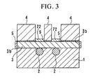
- a protective film 72 may be provided on buffer layer 3 on the parts on which electrodes 4 and 4 are not formed, and on the side surfaces 3b of buffer layer 3.
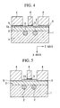
- a protective film 73 may be provided over the entirety of surface 3a of the buffer layer 3.
- a protective film 74 may be provided on buffer layer 3 on the portions on which electrodes 4 and 4 are not formed, and between the buffer layer 3 and one of the electrodes 4 and 4.
- a protective film 75 may be provided on the buffer layer 3 on the portions on which electrodes 4 and 4 are not formed.
- the surface 3a of the buffer layer 3 is not exposed, and it is difficult for the surface 3a of the buffer layer 3 and the inside of the buffer layer 3 to be contaminated.
- the protective film is made into an amorphous film having electrically insulating properties, and it is not particularly limited as long as it is able to prevent contamination of the buffer layer 3.
- a ferroelectric substrate 1 which comprises an X-cut lithium niobate.
- the ferroelectric substrate 1 comprises a single crystal having an electro-optic effect, and the axis which exhibits the electro-optic effect of the ferroelectric substrate 1 is in a direction parallel to the main face, it is suitable.
- a ferroelectric substrate 1 comprising a Y-cut lithium niobate may be used.
- the ferroelectric substrate is not limited to only lithium niobate, and it is possible to use lithium tantalate, for example.
- a transition metal layer 5 may be provided between the electrodes 4 and the protective film 7.
- the present invention is not limited to this, and a protective film 7 need not be provided.
- the buffer layer 3 comprises SiO 2 which has a low dielectric constant, and for the electrodes 4 to comprise Au which has a sufficiently low electrical resistance.
- the materials which form the buffer layer 3 and the electrodes 4 are not limited to the materials described above.
- the entire protective film may comprise a material.
- the present invention is not limited to this, and it is possible, for example, for the protective film provided on the buffer layer and the protective film provided on the side surfaces of the buffer layer to comprise different materials.
- the buffer layer 3 may be formed by means of a vacuum deposition method.
- this is not limited to a vacuum deposition method, and a buffer layer having high density formed by means of a high energy film forming method, such as sputtering, may be provided.
- the electro-optic element of the present invention due to individual differences caused in the manufacturing processes, it is possible for some regions of the buffer layer 3 of the electro-optic element on which electrodes 4 have not been formed to not be completely covered by the protective film. However, even if a protective film is not formed on a part of the region of buffer layer 3 on which electrodes 4 are not formed, the purposes of the present invention can still be obtained if the protective film is formed on almost all of the region of buffer layer 3 on which the electrodes 4 are not formed.
- optical waveguides 2 and 2 were formed by means of conducting a diffusion treatment for 20 hours at a 1000°C in an oxygen atmosphere on a diffused-type optical waveguide pattern comprising Ti and having a thickness of 90 nm, and thereon a SiO 2 film having a thickness of 1 ⁇ m was formed by vacuum deposition to form a buffer layer 3.
- a protective film 73 having a thickness of 100 nm and comprising Si was formed on the entire upper surface of buffer layer 3 by means of conducting radio frequency sputtering using silicon which had not been doped with impurities as the target, and using argon gas as the sputtering gas, with the ferroelectric substrate 1 at a temperature of 250°C.
- a transition metal film comprising Ti and having a thickness of 50 nm and an Au film having a thickness of 50 nm were consecutively formed by means of a vacuum deposition method within the same vacuum device.
- a resist pattern was formed on this Au film using photolithography technology, and electrodes 4 were formed only on the part on which the resist mask had not been formed, in other words, on the exposed part of the Au film by using an electroplating method.
- the resist mask was removed using an organic solvent, and the Au film which remained between the electrodes 4 and 4 was removed by etching using iodine potassium iodide and ammonia/hydrogen peroxide aqueous mix, and thereby, the optical waveguide modulator shown in FIG. 4 was obtained.
- a protective film 73 comprising Si 3 N 4 and having a thickness of 100 nm was formed in the same way as in Embodiment 1 using a gas mixture of Ar gas and nitrogen gas as the sputtering gas.
- a protective film 73 comprising SiC and having a thickness of 100 nm was formed in the same way as in Embodiment 1 using highly pure SiC as the target.
- optical waveguides 2 and 2 and a buffer layer 3 were formed in the same manner as in Embodiment 1. Then, after the whole of the ferroelectric substrate 1 was heat treated at 250°C within a sputtering device, the temperature was allowed to fall, and then a protective film 73 comprising Si and having a thickness of 100 nm was formed by means of a sputtering method at room temperature and using Ar gas as the sputtering gas.
- the protective film 73 displayed so-called semi-conductivity in which the electrical resistance decreases as the temperature increases, and the electrical resistance at room temperature was 30 to 40 M ⁇ .
- optical waveguides 2 and 2 and a buffer layer 3 were formed in the same manner as in Embodiment 1. Then, after the whole of the ferroelectric substrate 1 was heat treated at 250°C within a sputtering device, the temperature was allowed to fall, and then a protective film 7 comprising Si and having a thickness of 100 nm was formed by means of a sputtering method at room temperature and using Ar gas as the sputtering gas.
- the protective film 7 displayed so-called semi-conductivity in which the electrical resistance decreases as the temperature increases, and the electrical resistance at room temperature was 30 to 40 M ⁇ .
- the ferroelectric substrate 1 was cut to match the shape of a chip, the parts of the buffer layer 3 other than side surface 3b were protected using resist or the like, and a protective film 7 was formed on the side surfaces 3b of the buffer layer 3 by means of the same method as for the protective film 7 formed on the buffer layer 3. Thereby, an optical waveguide modulator as shown in FIG. 1 was obtained.
- optical waveguides 2 and 2 and a buffer layer 3 were formed in the same manner as in Embodiment 1. Then, a transition metal layer 5 and electrodes 4 were formed on the buffer layer 3 in the same way as in Embodiment 1 and thereby the optical waveguide modulator shown in FIG. 7 was obtained.
- Each of the buffer layers 3 of optical waveguide modulators of the Embodiment 1 to Embodiment 4, and the Conventional Example 1 obtained in the above-described ways were subjected to secondary ion mass spectrometry (SIMS) in the depth wise direction, and the contamination conditions of the buffer layers 3 were measured.
- SIMS secondary ion mass spectrometry
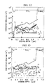
- FIG. 12 and FIG. 13 show graphs of the results of the secondary ion mass spectrometry (SIMS) measuring the contamination condition in the depth wise direction of the buffer layer 3 of Embodiment 1.
- FIGS. 14 and 15 show graphs of the results of the secondary ion mass spectrometry (SIMS) measuring the contamination condition in the depth wise direction of the buffer layer 3 of Conventional Example 1.
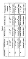
- Table 1 shows the amount of impurities which penetrated into the buffer layer 3 of Embodiments 1 to 5 and Conventional Example 1.
- the results of the secondary ion mass spectrometry in the depth wise direction of buffer layer 3 of the Conventional Example 1 indicate that contaminants such as K, B, Ti, Cr, Na (not shown in the figure), and H (not shown in the figure) were detected.
- these contaminants are localized in the surface 3a which is the exposed part of buffer layer 3, and a portion of the contaminants has penetrated into the inner part of buffer layer 3.
- K, B, Ti, and Na originate from the resist developing fluid and the washing fluid used in the manufacturing processes.
- the Ti is residue of the transition metal layer which was removed by etching.
- the Cr, and Ti were present in the etching fluid used to etch the Au film and the transition metal layer.
- the Li of FIGS. 12 to 15 is element diffused from the lithium niobate used to form the ferroelectric substrate 10.
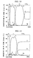
- compositional analysis in the depth wise direction from the buffer layer 3 to the electrodes 4 was conducted using an electron spectroscopic analysis device.
- FIGS. 10 and 11 The results are shown in FIGS. 10 and 11.
- FIG. 10 is a graph showing the results of the compositional analysis of Embodiment 1.
- FIG. 11 is a graph showing the results of the compositional analysis of the Conventional Example 1.
- the amount of oxygen which has penetrated into the transition metal layer 5 (Ti) is about 10 atomic percent.
- the amount of oxygen in the transition metal layer 5 (Ti) is below the limit of analysis.
- the optical waveguide modulators of Embodiment 4 and Conventional Example 1 were placed in thermoregulated bath of 120°C, initial dc biases of various levels were applied and the optical waveguide modulators were operated for 500 hours. While observing the modulation condition of the optical output signals using an oscilloscope, when the modulation condition is such that it is the same as when the initial dc bias was applied, the applied dc bias is feedback-controlled, and the modulation of that applied dc bias is recorded.
- FIG. 16 is a graph showing the modulation of the applied dc bias of Embodiment 4.
- FIG. 17 is a graph showing the modulation of the applied dc bias of the Conventional Example 1.
- the modulation condition was observed while the temperature of each of the optical waveguide modulators of Embodiment 4 and Conventional Example 1 were raised from 0°C to 70°C.
- the amount of variation in the modulation condition for both of Embodiment 4 and Conventional Example 1 was, in voltage, approximately 2V. From this, when the ferroelectric substrate 1 is an X-cut, it is clear that there is no negative effect originating from the pyroelectric charge due to variation in temperature even though the protective film 73 has semi-conductivity.
- the electro-optic element of the present invention since a protective film is provided on at least the region of the above-mentioned buffer layer on which the above-mentioned electrodes are not formed, the surface of the buffer layer is not exposed, and it is difficult for the surface of the buffer layer and the inside of the buffer layer to be contaminated with contaminants.
- this electro-optic element by providing a protective film over the whole of the above-mentioned buffer layer including the region on which the electrodes are formed, the entirety of the surface of the buffer layer is covered, and it is possible to prevent contamination of the buffer layer during the manufacturing process of the electro-optic element after the protective film has been formed.
- the protective film is formed on the entirety of the surface of the buffer layer, it is easier to form the protective film compared with a situation in which the protective film is formed on a part of the surface of the buffer layer.
Landscapes
- Physics & Mathematics (AREA)
- Nonlinear Science (AREA)
- Chemical & Material Sciences (AREA)
- Engineering & Computer Science (AREA)
- Ceramic Engineering (AREA)
- Crystallography & Structural Chemistry (AREA)
- General Physics & Mathematics (AREA)
- Optics & Photonics (AREA)
- Optical Modulation, Optical Deflection, Nonlinear Optics, Optical Demodulation, Optical Logic Elements (AREA)
- Optical Integrated Circuits (AREA)
Applications Claiming Priority (5)
| Application Number | Priority Date | Filing Date | Title |
|---|---|---|---|
| JP18251299 | 1999-06-28 | ||
| JP18251299 | 1999-06-28 | ||
| JP20828799 | 1999-07-22 | ||
| JP20828799 | 1999-07-22 | ||
| PCT/JP2000/004130 WO2001001190A1 (en) | 1999-06-28 | 2000-06-23 | Electrooptical device and method of manufacturing the same |
Publications (2)
| Publication Number | Publication Date |
|---|---|
| EP1197784A1 true EP1197784A1 (de) | 2002-04-17 |
| EP1197784A4 EP1197784A4 (de) | 2004-03-24 |
Family
ID=26501289
Family Applications (1)
| Application Number | Title | Priority Date | Filing Date |
|---|---|---|---|
| EP00939142A Withdrawn EP1197784A4 (de) | 1999-06-28 | 2000-06-23 | Elektrooptische vorrichtung und deren herstellungsverfahren |
Country Status (5)
| Country | Link |
|---|---|
| US (1) | US6583480B1 (de) |
| EP (1) | EP1197784A4 (de) |
| JP (1) | JP3401244B2 (de) |
| CA (1) | CA2377949C (de) |
| WO (1) | WO2001001190A1 (de) |
Cited By (1)
| Publication number | Priority date | Publication date | Assignee | Title |
|---|---|---|---|---|
| US6700691B2 (en) | 2001-05-14 | 2004-03-02 | Avanex Corporation | Electro-optic modulator having high bandwidth and low drive voltage |
Families Citing this family (5)
| Publication number | Priority date | Publication date | Assignee | Title |
|---|---|---|---|---|
| AU2002342855A1 (en) * | 2001-05-14 | 2002-11-25 | Corning O.T.I. Spa | Electro-optic modulator |
| US7408693B2 (en) * | 2004-07-27 | 2008-08-05 | Jds Uniphase Corporation | Electro-optic device |
| US7529433B2 (en) * | 2007-01-12 | 2009-05-05 | Jds Uniphase Corporation | Humidity tolerant electro-optic device |
| JP6578995B2 (ja) * | 2016-03-07 | 2019-09-25 | 住友大阪セメント株式会社 | 導波路型光素子 |
| CN112764244B (zh) * | 2021-01-26 | 2022-05-17 | 济南晶正电子科技有限公司 | 一种电光晶体薄膜、制备方法及电子元器件 |
Family Cites Families (19)
| Publication number | Priority date | Publication date | Assignee | Title |
|---|---|---|---|---|
| JPS6147929A (ja) * | 1984-08-15 | 1986-03-08 | Jido Keisoku Gijutsu Kenkiyuukumiai | 光電圧センサ |
| JPS6273207A (ja) | 1985-09-27 | 1987-04-03 | Fujitsu Ltd | 導波路光デイバイス |
| JPS62173428A (ja) | 1986-01-28 | 1987-07-30 | Fujitsu Ltd | 導波路光デバイス |
| US4917451A (en) * | 1988-01-19 | 1990-04-17 | E. I. Dupont De Nemours And Company | Waveguide structure using potassium titanyl phosphate |
| JP2686764B2 (ja) * | 1988-03-11 | 1997-12-08 | 国際電信電話株式会社 | 光半導体素子の製造方法 |
| JPH03249626A (ja) * | 1990-02-27 | 1991-11-07 | Shimadzu Corp | 光ic素子 |
| JP2867560B2 (ja) * | 1990-03-02 | 1999-03-08 | 富士通株式会社 | 光導波路デバイス |
| JP3021888B2 (ja) * | 1991-12-04 | 2000-03-15 | 住友金属鉱山株式会社 | 光導波路機能素子及びその製造方法 |
| DE69226761T2 (de) * | 1991-12-27 | 1999-01-14 | Fujitsu Ltd., Kawasaki, Kanagawa | Optische Wellenleiteranordnung mit reduzierter DC-Drift |
| JPH06274954A (ja) * | 1993-01-25 | 1994-09-30 | Shin Etsu Chem Co Ltd | 光磁気記録媒体の製造方法 |
| JPH07168042A (ja) * | 1993-12-15 | 1995-07-04 | Nikon Corp | 光制御デバイスおよびその製造方法 |
| JP2894961B2 (ja) * | 1994-11-18 | 1999-05-24 | 日本電気株式会社 | 光制御デバイス |
| JP2674535B2 (ja) * | 1994-12-15 | 1997-11-12 | 日本電気株式会社 | 光制御デバイス |
| JP3544020B2 (ja) * | 1995-01-13 | 2004-07-21 | 富士通株式会社 | 光導波路デバイスの製造方法 |
| JP3287982B2 (ja) * | 1995-09-08 | 2002-06-04 | シャープ株式会社 | 信号処理回路を内蔵する光導波路型光検出器およびその製造方法 |
| JPH09281454A (ja) * | 1996-04-12 | 1997-10-31 | Nec Corp | 導波路型光変調器 |
| DE69737430T2 (de) * | 1996-06-14 | 2007-11-29 | Sumitomo Osaka Cement Co., Ltd. | Optischer Wellenleitermodulator mit Wanderwellenelektroden |
| JP2801900B2 (ja) | 1996-10-31 | 1998-09-21 | 住友大阪セメント株式会社 | 導波路型光変調器 |
| JP3362105B2 (ja) * | 1997-03-31 | 2003-01-07 | 住友大阪セメント株式会社 | 導波路型光変調器 |
-
2000
- 2000-06-23 JP JP2001507138A patent/JP3401244B2/ja not_active Expired - Fee Related
- 2000-06-23 EP EP00939142A patent/EP1197784A4/de not_active Withdrawn
- 2000-06-23 CA CA002377949A patent/CA2377949C/en not_active Expired - Fee Related
- 2000-06-23 WO PCT/JP2000/004130 patent/WO2001001190A1/ja not_active Ceased
- 2000-06-23 US US10/019,010 patent/US6583480B1/en not_active Expired - Fee Related
Cited By (1)
| Publication number | Priority date | Publication date | Assignee | Title |
|---|---|---|---|---|
| US6700691B2 (en) | 2001-05-14 | 2004-03-02 | Avanex Corporation | Electro-optic modulator having high bandwidth and low drive voltage |
Also Published As
| Publication number | Publication date |
|---|---|
| US6583480B1 (en) | 2003-06-24 |
| CA2377949C (en) | 2005-10-25 |
| EP1197784A4 (de) | 2004-03-24 |
| CA2377949A1 (en) | 2001-01-04 |
| WO2001001190A1 (en) | 2001-01-04 |
| JP3401244B2 (ja) | 2003-04-28 |
Similar Documents
| Publication | Publication Date | Title |
|---|---|---|
| US6956980B2 (en) | Optical waveguide type optical modulator and production method therefor | |
| US6583480B1 (en) | Electro-optical element having protective film on top and side surfaces of buffer layer | |
| JP5072232B2 (ja) | バイアス点直流電圧ドリフトおよび熱偏移抑制式の電気光学導波路素子とその製造方法 | |
| US6195191B1 (en) | Optical devices having improved temperature stability | |
| JP3710686B2 (ja) | 電気光学素子 | |
| JPS59141271A (ja) | 薄膜トランジスタ | |
| US6282356B1 (en) | Optical waveguide device with enhanced stability | |
| CN115516368B (zh) | 电光元件用复合基板 | |
| US6436614B1 (en) | Method for the formation of a thin optical crystal layer overlying a low dielectric constant substrate | |
| JPWO2001001190A1 (ja) | 電気光学素子およびその製造方法 | |
| JP3153110B2 (ja) | 導波路型低dcドリフト性光変調器の製造方法 | |
| CA2369673C (en) | A method for fabricating an optical waveguide device | |
| JP3021888B2 (ja) | 光導波路機能素子及びその製造方法 | |
| JP3231190B2 (ja) | 導波路型光素子 | |
| JP3228823B2 (ja) | 導波路型光素子、およびその製造方法 | |
| JPH01114080A (ja) | 薄膜トランジスタ | |
| JP3050202B2 (ja) | 光導波路デバイスおよびその製造方法 | |
| JP2004302191A (ja) | 光制御素子 | |
| JP3932242B2 (ja) | 光導波路素子の形成方法 | |
| Nagata et al. | Process control for a SiO2 buffer layer of LiNbO3 modulators to obtain reduced dc drift performance | |
| WO2013015294A1 (ja) | 光導波路素子 | |
| JPH09269469A (ja) | 光導波路デバイス | |
| JP2002202483A (ja) | 光導波路素子の作製方法 |
Legal Events
| Date | Code | Title | Description |
|---|---|---|---|
| PUAI | Public reference made under article 153(3) epc to a published international application that has entered the european phase |
Free format text: ORIGINAL CODE: 0009012 |
|
| 17P | Request for examination filed |
Effective date: 20011231 |
|
| AK | Designated contracting states |
Kind code of ref document: A1 Designated state(s): AT BE CH CY DE DK ES FI FR GB GR IE IT LI LU MC NL PT SE |
|
| A4 | Supplementary search report drawn up and despatched |
Effective date: 20040209 |
|
| RBV | Designated contracting states (corrected) |
Designated state(s): DE FR GB |
|
| 17Q | First examination report despatched |
Effective date: 20040512 |
|
| STAA | Information on the status of an ep patent application or granted ep patent |
Free format text: STATUS: THE APPLICATION IS DEEMED TO BE WITHDRAWN |
|
| 18D | Application deemed to be withdrawn |
Effective date: 20040923 |