EP1197758A2 - Integrierter Halbleiterbaustein mit überbrückbarem Eingangs-Tiefpassfilter - Google Patents
Integrierter Halbleiterbaustein mit überbrückbarem Eingangs-Tiefpassfilter Download PDFInfo
- Publication number
- EP1197758A2 EP1197758A2 EP01122715A EP01122715A EP1197758A2 EP 1197758 A2 EP1197758 A2 EP 1197758A2 EP 01122715 A EP01122715 A EP 01122715A EP 01122715 A EP01122715 A EP 01122715A EP 1197758 A2 EP1197758 A2 EP 1197758A2
- Authority
- EP
- European Patent Office
- Prior art keywords
- pass filter
- bus
- multiplexer
- connection
- output
- Prior art date
- Legal status (The legal status is an assumption and is not a legal conclusion. Google has not performed a legal analysis and makes no representation as to the accuracy of the status listed.)
- Granted
Links
Images
Classifications
-
- G—PHYSICS
- G01—MEASURING; TESTING
- G01R—MEASURING ELECTRIC VARIABLES; MEASURING MAGNETIC VARIABLES
- G01R31/00—Arrangements for testing electric properties; Arrangements for locating electric faults; Arrangements for electrical testing characterised by what is being tested not provided for elsewhere
- G01R31/28—Testing of electronic circuits, e.g. by signal tracer
- G01R31/317—Testing of digital circuits
- G01R31/3181—Functional testing
- G01R31/3185—Reconfiguring for testing, e.g. LSSD, partitioning
- G01R31/318533—Reconfiguring for testing, e.g. LSSD, partitioning using scanning techniques, e.g. LSSD, Boundary Scan, JTAG
-
- G—PHYSICS
- G01—MEASURING; TESTING
- G01R—MEASURING ELECTRIC VARIABLES; MEASURING MAGNETIC VARIABLES
- G01R31/00—Arrangements for testing electric properties; Arrangements for locating electric faults; Arrangements for electrical testing characterised by what is being tested not provided for elsewhere
- G01R31/28—Testing of electronic circuits, e.g. by signal tracer
- G01R31/317—Testing of digital circuits
- G01R31/3181—Functional testing
- G01R31/3185—Reconfiguring for testing, e.g. LSSD, partitioning
- G01R31/318505—Test of Modular systems, e.g. Wafers, MCM's
Definitions
- the present invention relates to an integrated semiconductor device according to the features of the preamble of the claim 1.
- IIC integrated semiconductor components
- An essential step in the manufacture of integrated Semiconductor components is the test of the manufactured components IC for accuracy. As many or as many as possible Settings that are possible in the integrated circuit made and checked.
- the test of the IC should be as possible take little time. To test on an IC to be able to carry out additional circuit measures in the IC required. The effort for these circuit measures should also be kept as low as possible, that is the additional circuitry measures that are usually only should be needed once during the life of the IC as little as possible of the available chip area consume.
- the use of the IIC bus for making settings on the IC during the test has so far been unfavorable because the Bandwidth for data exchange via the IIC bus using a low pass filter limited to 100 kHz or 400 kHz is. This is used during the later operation of the IC high-frequency interference signals on the data bus, for example can occur when using the IC in television sets, filter out.
- the aim of the present invention is to provide an integrated Semiconductor device to provide a fast Testing with little additional circuitry allows.
- the semiconductor module according to the invention has a connection for connection to a data bus and the connection downstream low-pass filter a bypass circuitry to bypass the low pass filter.
- the data bus is preferably an IIC bus.
- connection for feeding the test samples with high Clock rates of the existing connection pin for the data bus used is the one required for testing purposes Circuit complexity of the IC according to the invention is low.
- the circuit arrangement for bridging the low-pass filter preferably has a demultiplexer and a multiplexer on, with the demultiplexer upstream of the low-pass filter and the multiplexer is connected downstream of the low-pass filter is.
- An input of the demultiplexer is preferred connected to the data bus and a first output of the Demultiplexer is connected to an input of the low pass filter.
- An output of the low pass filter is still on a first input of the multiplexer connected, wherein a second input of the multiplexer for bridging the Low pass filter to a second output of the demultiplexer connected.
- the semiconductor module preferably has a controller circuit that supports testing the device.
- the Controller circuit maps the connector pins of the IC during functions for the test, which are for test purposes only serve and differ from the functions during normal operation differ. So you can use the connection pins during the test, for example, the values of internal registers or internal clock signals are output to check whether the respective registers or clock generators are working correctly.
- the multiplexers and demultiplexers are according to one embodiment of the invention can be controlled by the controller circuit, to bypass the low pass filter for testing purposes.
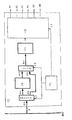
- FIG. 1 shows a block diagram of an integrated according to the invention Semiconductor device.
- the semiconductor module has an input IN, which is connected to a Data bus BUS, preferably an IIC bus connected is.
- Connections (connection pins) P1, P2, P3, P4, P5, P6 are used for connection to external components, which further integrated Circuits can be.
- At these connection pins P1, P2, P3, P4, P5, P6 are output variables, for example Control of the external components or input variables, which processes in the integrated semiconductor chip IC become available.
- a processing unit VE the has a plurality of circuit components.
- the integrated semiconductor module also has one Interface circuit IFC on which to the processing unit is connected and which is the data exchange between controls the processing unit VE and the bus.
- the Processing unit VE are via the interface circuit IFC data is supplied from the bus, and over the interface unit is used to output data from the Processing unit VE to the bus.
- the interface circuit IFC is a conventional one when using an IIC bus so-called IIC interface.
- TP Low pass filter
- the integrated semiconductor circuit has a Circuit arrangement for bridging the low-pass filter TP for testing purposes.
- This circuit arrangement shows in the Embodiment according to Figure 1 a demultiplexer DEMUX1 on that between the the input IN and the low pass filter TP is switched.
- a demultiplexer DEMUX1 on that between the the input IN and the low pass filter TP is switched.
- the circuit arrangement for short-circuiting also has one Multiplexer MUX2 on between the low pass filter TP and the interface circuit IFC is connected, wherein a Input of the multiplexer MUX2 to an output of the low pass filter TP and an output A21 of the multiplexer to the Interface circuit IFC is connected.
- a second Output A12 of the demultiplexer DEMUX1 to a second one Input E22 of multiplexer MUX2 is connected to bridge of the low-pass filter TP.
- the demultiplexer DEMUX1 and the multiplexer MUX2 are controlled by an existing one for testing the IC module Controller circuit connected to control inputs C1, C2 of the multiplexer connected.
- the demultiplexer DEMUX1 Input E11 connected to the first output A11 to the data from the bus to the low pass filter
- the first Input E21 of multiplexer MUX2 is at its output A21 connected to the output data of the low-pass filter TP the interface circuit IFC and thus the processing unit supply.
- the multiplexers DEMUX1, MUX2 controlled by the controller circuit TC in such a way that the data from the bus via the second output A12 of the Demultiplexer DEMUX1 and the second input E22 of the multiplexer MUX2 unfiltered to the IFC interface circuit, or the processing unit VE.
- test the module it is necessary to use the module all or as many settings or initializations as possible, that are possible to make.
- By bridging the Low pass filters TP can provide the IC with the appropriate test Control commands with a much higher clock frequency than are supplied during normal operation.
- the test of the module according to the invention can thus be carried out in a short time Time using the existing connection pin IN for the data bus.
- TAP controller supports the process the test of the integrated module IC.
- the TAP controller is next to the multiplexers DEMUX1, MUX2 also to the processing unit VE connected and assigns the connection pins P1, P2, P3, P4, P5, P6 during the test other functions than during normal operation too. For example during testing the values of internal registers or the Signals from internal clock generators via the connection pins P1 ... P6 must be given to the outside to ensure proper Check the functioning of these components.
- the circuit arrangement according to the invention for bridging the Low pass filter thus enables a quick test of the integrated Semiconductor device using the anyway existing connection IN of the integrated module for the Data bus.
- the hardware expenditure for the circuit arrangement is with a demultiplexer and a multiplexer DEMUX1, MUX2 small and easy to implement. It can also be used for control the demultiplexer DEMUX1 and the multiplexer MUX2 anyway Existing TAP controllers can be used for testing.
Landscapes
- Engineering & Computer Science (AREA)
- General Engineering & Computer Science (AREA)
- Physics & Mathematics (AREA)
- General Physics & Mathematics (AREA)
- Tests Of Electronic Circuits (AREA)
- Semiconductor Integrated Circuits (AREA)
Abstract
Description
- A11, A12
- Ausgänge des ersten Multiplexers
- A21
- Ausgang des zweiten Multiplexers
- BUS
- Bus
- C1
- Steueranschluss des ersten Multiplexers
- C2
- Steueranschluss des zweiten Multiplexers
- E11
- erster Eingang des ersten Multiplexers
- E21, E22
- Eingänge des zweiten Multiplexers
- IC
- integrierter Halbleiterbaustein
- IFC
- Schnittstellenschaltung
- IN
- Eingang des IC
- DEMUX1
- Demultiplexer
- MUX2
- Multiplexer
- P1 - P6
- Anschlusspins des IC
- TP
- Tiefpassfilter
- VE
- Verarbeitungseinheit
Claims (5)
- Integrierter Halbleiterbaustein mit wenigstens einem Anschluss (IN) zum Anschließen an einen Datenbus (BUS) und ein dem Anschluss (IN) nachgeschaltetes Tiefpassfilter (TP), dadurch gekennzeichnet, dass eine Schaltungsanordnung (DEMUX1, MUX2) zum Überbrücken des Tiefpassfilters (TP) zu Testzwecken vorgesehen ist.
- Integrierter Halbleiterbaustein nach Anspruch 1, bei dem der wenigstens eine Anschluss (IN) zum Anschließen an einen IIC-Bus ausgebildet ist.
- Integrierter Halbleiterbaustein, bei dem die Überbrückungsschaltungsanordnung folgende Merkmale aufweist:einen Demultiplexer (DEMUX1) mit einem Eingang (E11), der an den wenigstens einen Eingang (IN) angeschlossen ist, einem ersten Ausgang (A11), der an das Tiefpassfilter (TP) angeschlossen ist und mit einem zweiten Ausgang (A12) ;einen Multiplexer (MUX2) mit einem ersten Eingang (E21), der an das Tiefpassfilter (TP) angeschlossen ist, einem zweiten Eingang (E22), der an den zweiten Ausgang (A12) des Demultiplexers (DEMUX1) angeschlossen ist und mit einem Ausgang (A21).
- Integrierter Halbleiterbaustein nach Anspruch 3, bei dem der Ausgang (A21) des Multiplexers (MUX2) an eine Schnittstellenschaltung (IFC) zur Weiterverarbeitung der über den Datenbus (BUS) empfangenen Daten oder zur Bereitstellung der über den Datenbus (BUS) zu sendenden Daten aufweist.
- Integrierter Halbleiterbaustein nach einem der vorangehenden Ansprüche, der einen zu Testzwecken vorhandenen Controller (TC) aufweist, wobei der Controller (TC) an den Demultiplexer (DEMUX1) und den Multiplexer (MUX2) zu deren Ansteuerung angeschlossen ist.
Applications Claiming Priority (2)
| Application Number | Priority Date | Filing Date | Title |
|---|---|---|---|
| DE10051100A DE10051100C1 (de) | 2000-10-14 | 2000-10-14 | Integrierter Halbleiterbaustein mit überbrückbarem Eingangs-Tiefpassfilter |
| DE10051100 | 2000-10-14 |
Publications (3)
| Publication Number | Publication Date |
|---|---|
| EP1197758A2 true EP1197758A2 (de) | 2002-04-17 |
| EP1197758A3 EP1197758A3 (de) | 2004-03-31 |
| EP1197758B1 EP1197758B1 (de) | 2005-11-30 |
Family
ID=7659880
Family Applications (1)
| Application Number | Title | Priority Date | Filing Date |
|---|---|---|---|
| EP01122715A Expired - Lifetime EP1197758B1 (de) | 2000-10-14 | 2001-09-21 | Integrierter Halbleiterbaustein mit überbrückbarem Eingangs-Tiefpassfilter |
Country Status (3)
| Country | Link |
|---|---|
| US (1) | US6759890B2 (de) |
| EP (1) | EP1197758B1 (de) |
| DE (2) | DE10051100C1 (de) |
Families Citing this family (1)
| Publication number | Priority date | Publication date | Assignee | Title |
|---|---|---|---|---|
| SG108251A1 (en) * | 2001-05-03 | 2005-01-28 | Ibm | Innovative bypass circuit for circuit testing and modification |
Family Cites Families (6)
| Publication number | Priority date | Publication date | Assignee | Title |
|---|---|---|---|---|
| JPS5873881A (ja) * | 1981-10-29 | 1983-05-04 | Advantest Corp | Icテスタ |
| US4779273A (en) * | 1984-06-14 | 1988-10-18 | Data General Corporation | Apparatus for self-testing a digital logic circuit |
| DE3821230A1 (de) * | 1988-06-23 | 1989-12-28 | Siemens Ag | Testanordnung zur erzeugung von testmustern fuer den test von mikroprozessoren |
| DE69115338T2 (de) * | 1990-04-20 | 1996-05-09 | Texas Instruments Inc | Abtasttestschaltung zur Verwendung mit Mehrfrequenzschaltungen |
| US5744991A (en) * | 1995-10-16 | 1998-04-28 | Altera Corporation | System for distributing clocks using a delay lock loop in a programmable logic circuit |
| US6559715B1 (en) * | 1999-08-13 | 2003-05-06 | Xilinx, Inc. | Low pass filter |
-
2000
- 2000-10-14 DE DE10051100A patent/DE10051100C1/de not_active Expired - Fee Related
-
2001
- 2001-09-21 DE DE50108229T patent/DE50108229D1/de not_active Expired - Lifetime
- 2001-09-21 EP EP01122715A patent/EP1197758B1/de not_active Expired - Lifetime
- 2001-10-15 US US09/977,788 patent/US6759890B2/en not_active Expired - Lifetime
Also Published As
| Publication number | Publication date |
|---|---|
| EP1197758A3 (de) | 2004-03-31 |
| US6759890B2 (en) | 2004-07-06 |
| US20020053913A1 (en) | 2002-05-09 |
| DE50108229D1 (de) | 2006-01-05 |
| DE10051100C1 (de) | 2002-07-11 |
| EP1197758B1 (de) | 2005-11-30 |
Similar Documents
| Publication | Publication Date | Title |
|---|---|---|
| DE69628143T2 (de) | Jtag-prüfung eines busses unter verwendung von einsteckkarten mit jtag-logikschaltung | |
| DE3130714C2 (de) | ||
| DE3727723C2 (de) | Verfahren zur Prüfung eines Trägers mit mehreren integrierten Digitalschaltungen, geeignete integrierte Schaltung zum Anbringen auf einem auf diese Weise zu prüfenden Träger und Träger mit mehreren derartigen integrierten Schaltungen | |
| DE602004003475T2 (de) | Testen von integrierten schaltungen | |
| DE69429741T2 (de) | Analoge, selbstständige Prüfbusstruktur zum Testen integrierter Schaltungen auf einer gedruckten Leiterplatte | |
| DE102010012904B4 (de) | Systeme zum Durchführen eines Tests | |
| DE102010016175A1 (de) | Batterieüberwachungs- und -Steuerungsvorrichtung sowie Verfahren zu deren Verwendung | |
| DE3702408C2 (de) | ||
| DE10138556C1 (de) | Verfahren zum Testen von Eingangs-/Ausgangstreibern einer Schaltung und entsprechende Testvorrichtung | |
| EP1427086A1 (de) | Elektrisches Gerät und Verfahren zum Betreiben eines elektrischen Geräts | |
| DE19536226A1 (de) | Testbare Schaltungsanordnung mit mehreren identischen Schaltungsblöcken | |
| DE3146721C2 (de) | ||
| DE10306620B4 (de) | Integrierte Testschaltung in einer integrierten Schaltung | |
| DE69026809T2 (de) | Verfahren zur Treibersteuerung integrierter Schaltungen während der Prüfung | |
| DE19903606B4 (de) | Halbleiteranordnung | |
| EP1197758B1 (de) | Integrierter Halbleiterbaustein mit überbrückbarem Eingangs-Tiefpassfilter | |
| DE69932915T2 (de) | Prüfschaltung für ein Telekommunikationselement | |
| DE60026093T2 (de) | Halbleitervorrichtung mit Makros und Prüfverfahren dafür | |
| DE60309128T2 (de) | LSI-Testanordnung | |
| DE102006011706B4 (de) | Halbleiter-Bauelement, sowie Halbleiter-Bauelement-Test-Verfahren | |
| EP1221097B1 (de) | Schaltungszelle zur testmuster-generierung und testmuster-kompression | |
| EP0638185B1 (de) | Verfahren zum prüfen von mit einer vielzahl von unterschiedlichen bausteinen bestückten baugruppen | |
| DE102004059505B4 (de) | Anordnung zum Test von eingebetteten Schaltungen mit Hilfe von Testinseln | |
| DE10330037B3 (de) | Adapterkarte zum Anschließen an einen Datenbus in einer Datenverarbeitungseinheit und Verfahren zum Betreiben eines DDR-Speichermoduls | |
| DE102006033188A1 (de) | Halbleiterbauelement, Testplatine, Testsystem, und Testverfahren |
Legal Events
| Date | Code | Title | Description |
|---|---|---|---|
| PUAI | Public reference made under article 153(3) epc to a published international application that has entered the european phase |
Free format text: ORIGINAL CODE: 0009012 |
|
| AK | Designated contracting states |
Kind code of ref document: A2 Designated state(s): AT BE CH CY DE DK ES FI FR GB GR IE IT LI LU MC NL PT SE TR |
|
| AX | Request for extension of the european patent |
Free format text: AL;LT;LV;MK;RO;SI |
|
| PUAL | Search report despatched |
Free format text: ORIGINAL CODE: 0009013 |
|
| AK | Designated contracting states |
Kind code of ref document: A3 Designated state(s): AT BE CH CY DE DK ES FI FR GB GR IE IT LI LU MC NL PT SE TR |
|
| AX | Request for extension of the european patent |
Extension state: AL LT LV MK RO SI |
|
| 17P | Request for examination filed |
Effective date: 20040315 |
|
| 17Q | First examination report despatched |
Effective date: 20040601 |
|
| AKX | Designation fees paid |
Designated state(s): DE FR IT |
|
| GRAP | Despatch of communication of intention to grant a patent |
Free format text: ORIGINAL CODE: EPIDOSNIGR1 |
|
| GRAS | Grant fee paid |
Free format text: ORIGINAL CODE: EPIDOSNIGR3 |
|
| GRAA | (expected) grant |
Free format text: ORIGINAL CODE: 0009210 |
|
| AK | Designated contracting states |
Kind code of ref document: B1 Designated state(s): DE FR IT |
|
| REF | Corresponds to: |
Ref document number: 50108229 Country of ref document: DE Date of ref document: 20060105 Kind code of ref document: P |
|
| ET | Fr: translation filed | ||
| PLBE | No opposition filed within time limit |
Free format text: ORIGINAL CODE: 0009261 |
|
| STAA | Information on the status of an ep patent application or granted ep patent |
Free format text: STATUS: NO OPPOSITION FILED WITHIN TIME LIMIT |
|
| 26N | No opposition filed |
Effective date: 20060831 |
|
| PGFP | Annual fee paid to national office [announced via postgrant information from national office to epo] |
Ref country code: IT Payment date: 20150924 Year of fee payment: 15 |
|
| REG | Reference to a national code |
Ref country code: FR Ref legal event code: PLFP Year of fee payment: 16 |
|
| PG25 | Lapsed in a contracting state [announced via postgrant information from national office to epo] |
Ref country code: IT Free format text: LAPSE BECAUSE OF NON-PAYMENT OF DUE FEES Effective date: 20160921 |
|
| REG | Reference to a national code |
Ref country code: FR Ref legal event code: PLFP Year of fee payment: 17 |
|
| REG | Reference to a national code |
Ref country code: FR Ref legal event code: PLFP Year of fee payment: 18 |
|
| PGFP | Annual fee paid to national office [announced via postgrant information from national office to epo] |
Ref country code: DE Payment date: 20191121 Year of fee payment: 19 |
|
| PGFP | Annual fee paid to national office [announced via postgrant information from national office to epo] |
Ref country code: FR Payment date: 20200914 Year of fee payment: 20 |
|
| REG | Reference to a national code |
Ref country code: DE Ref legal event code: R119 Ref document number: 50108229 Country of ref document: DE |
|
| PG25 | Lapsed in a contracting state [announced via postgrant information from national office to epo] |
Ref country code: DE Free format text: LAPSE BECAUSE OF NON-PAYMENT OF DUE FEES Effective date: 20210401 |