EP1196016A2 - Wiring substrate and manufacturing method of the same along with electroless copper plating solution used therefor - Google Patents
Wiring substrate and manufacturing method of the same along with electroless copper plating solution used therefor Download PDFInfo
- Publication number
- EP1196016A2 EP1196016A2 EP01123229A EP01123229A EP1196016A2 EP 1196016 A2 EP1196016 A2 EP 1196016A2 EP 01123229 A EP01123229 A EP 01123229A EP 01123229 A EP01123229 A EP 01123229A EP 1196016 A2 EP1196016 A2 EP 1196016A2
- Authority
- EP
- European Patent Office
- Prior art keywords
- plating solution
- plating
- copper
- mol
- plated film
- Prior art date
- Legal status (The legal status is an assumption and is not a legal conclusion. Google has not performed a legal analysis and makes no representation as to the accuracy of the status listed.)
- Withdrawn
Links
- 238000007747 plating Methods 0.000 title claims abstract description 399
- 239000000758 substrate Substances 0.000 title claims abstract description 218
- RYGMFSIKBFXOCR-UHFFFAOYSA-N Copper Chemical compound [Cu] RYGMFSIKBFXOCR-UHFFFAOYSA-N 0.000 title claims abstract description 156
- 229910052802 copper Inorganic materials 0.000 title claims abstract description 151
- 239000010949 copper Substances 0.000 title claims abstract description 151
- 238000004519 manufacturing process Methods 0.000 title claims description 70
- 238000000034 method Methods 0.000 claims abstract description 92
- NNICRUQPODTGRU-UHFFFAOYSA-N mandelonitrile Chemical compound N#CC(O)C1=CC=CC=C1 NNICRUQPODTGRU-UHFFFAOYSA-N 0.000 claims abstract description 88
- ROFVEXUMMXZLPA-UHFFFAOYSA-N Bipyridyl Chemical group N1=CC=CC=C1C1=CC=CC=N1 ROFVEXUMMXZLPA-UHFFFAOYSA-N 0.000 claims abstract description 47
- 239000000654 additive Substances 0.000 claims abstract description 45
- 239000003795 chemical substances by application Substances 0.000 claims abstract description 45
- 230000000996 additive effect Effects 0.000 claims abstract description 44
- SXYCCJAPZKHOLS-UHFFFAOYSA-N chembl2008674 Chemical compound [O-][N+](=O)C1=CC=C2C(N=NC3=C4C=CC=CC4=CC=C3O)=C(O)C=C(S(O)(=O)=O)C2=C1 SXYCCJAPZKHOLS-UHFFFAOYSA-N 0.000 claims abstract description 37
- IYRGXJIJGHOCFS-UHFFFAOYSA-N neocuproine Chemical compound C1=C(C)N=C2C3=NC(C)=CC=C3C=CC2=C1 IYRGXJIJGHOCFS-UHFFFAOYSA-N 0.000 claims abstract description 23
- DGEZNRSVGBDHLK-UHFFFAOYSA-N [1,10]phenanthroline Chemical compound C1=CN=C2C3=NC=CC=C3C=CC2=C1 DGEZNRSVGBDHLK-UHFFFAOYSA-N 0.000 claims abstract description 18
- JPVYNHNXODAKFH-UHFFFAOYSA-N Cu2+ Chemical compound [Cu+2] JPVYNHNXODAKFH-UHFFFAOYSA-N 0.000 claims description 22
- 229910001431 copper ion Inorganic materials 0.000 claims description 22
- 239000003638 chemical reducing agent Substances 0.000 claims description 17
- 239000008139 complexing agent Substances 0.000 claims description 9
- -1 triethyltetramine Chemical compound 0.000 claims description 2
- 239000000243 solution Substances 0.000 description 210
- HEMHJVSKTPXQMS-UHFFFAOYSA-M Sodium hydroxide Chemical compound [OH-].[Na+] HEMHJVSKTPXQMS-UHFFFAOYSA-M 0.000 description 160
- 230000008021 deposition Effects 0.000 description 151
- WSFSSNUMVMOOMR-UHFFFAOYSA-N Formaldehyde Chemical compound O=C WSFSSNUMVMOOMR-UHFFFAOYSA-N 0.000 description 111
- 230000000704 physical effect Effects 0.000 description 102
- 238000012360 testing method Methods 0.000 description 61
- 235000011121 sodium hydroxide Nutrition 0.000 description 54
- 239000000203 mixture Substances 0.000 description 51
- 230000000694 effects Effects 0.000 description 50
- 239000010410 layer Substances 0.000 description 46
- 239000007788 liquid Substances 0.000 description 31
- 230000008569 process Effects 0.000 description 30
- 238000011156 evaluation Methods 0.000 description 28
- KCXVZYZYPLLWCC-UHFFFAOYSA-N EDTA Chemical compound OC(=O)CN(CC(O)=O)CCN(CC(O)=O)CC(O)=O KCXVZYZYPLLWCC-UHFFFAOYSA-N 0.000 description 27
- 229960001484 edetic acid Drugs 0.000 description 27
- JZCCFEFSEZPSOG-UHFFFAOYSA-L copper(II) sulfate pentahydrate Chemical compound O.O.O.O.O.[Cu+2].[O-]S([O-])(=O)=O JZCCFEFSEZPSOG-UHFFFAOYSA-L 0.000 description 26
- 238000011077 uniformity evaluation Methods 0.000 description 21
- 230000000052 comparative effect Effects 0.000 description 18
- 239000002202 Polyethylene glycol Substances 0.000 description 15
- 230000006872 improvement Effects 0.000 description 15
- 229920001223 polyethylene glycol Polymers 0.000 description 15
- 238000012545 processing Methods 0.000 description 9
- 230000008901 benefit Effects 0.000 description 8
- 238000006243 chemical reaction Methods 0.000 description 8
- HHLFWLYXYJOTON-UHFFFAOYSA-N glyoxylic acid Chemical compound OC(=O)C=O HHLFWLYXYJOTON-UHFFFAOYSA-N 0.000 description 8
- 230000035939 shock Effects 0.000 description 8
- 230000007423 decrease Effects 0.000 description 7
- 238000005259 measurement Methods 0.000 description 7
- 239000003002 pH adjusting agent Substances 0.000 description 7
- 239000011889 copper foil Substances 0.000 description 6
- 239000000463 material Substances 0.000 description 6
- 150000001879 copper Chemical class 0.000 description 5
- 239000011229 interlayer Substances 0.000 description 5
- CURLTUGMZLYLDI-UHFFFAOYSA-N Carbon dioxide Chemical compound O=C=O CURLTUGMZLYLDI-UHFFFAOYSA-N 0.000 description 4
- 239000007864 aqueous solution Substances 0.000 description 4
- 229910052751 metal Inorganic materials 0.000 description 4
- 239000002184 metal Substances 0.000 description 4
- 229920001515 polyalkylene glycol Polymers 0.000 description 4
- 239000012048 reactive intermediate Substances 0.000 description 4
- 230000009467 reduction Effects 0.000 description 4
- VILCJCGEZXAXTO-UHFFFAOYSA-N 2,2,2-tetramine Chemical compound NCCNCCNCCN VILCJCGEZXAXTO-UHFFFAOYSA-N 0.000 description 3
- 239000004593 Epoxy Substances 0.000 description 3
- VEXZGXHMUGYJMC-UHFFFAOYSA-N Hydrochloric acid Chemical compound Cl VEXZGXHMUGYJMC-UHFFFAOYSA-N 0.000 description 3
- WMFOQBRAJBCJND-UHFFFAOYSA-M Lithium hydroxide Chemical compound [Li+].[OH-] WMFOQBRAJBCJND-UHFFFAOYSA-M 0.000 description 3
- KWYUFKZDYYNOTN-UHFFFAOYSA-M Potassium hydroxide Chemical compound [OH-].[K+] KWYUFKZDYYNOTN-UHFFFAOYSA-M 0.000 description 3
- 239000003054 catalyst Substances 0.000 description 3
- 238000010586 diagram Methods 0.000 description 3
- 238000005530 etching Methods 0.000 description 3
- 239000011521 glass Substances 0.000 description 3
- 230000010354 integration Effects 0.000 description 3
- 238000001556 precipitation Methods 0.000 description 3
- 238000005406 washing Methods 0.000 description 3
- ICSNLGPSRYBMBD-UHFFFAOYSA-N 2-aminopyridine Chemical compound NC1=CC=CC=N1 ICSNLGPSRYBMBD-UHFFFAOYSA-N 0.000 description 2
- BSKHPKMHTQYZBB-UHFFFAOYSA-N 2-methylpyridine Chemical compound CC1=CC=CC=N1 BSKHPKMHTQYZBB-UHFFFAOYSA-N 0.000 description 2
- 229920001342 Bakelite® Polymers 0.000 description 2
- KDLHZDBZIXYQEI-UHFFFAOYSA-N Palladium Chemical compound [Pd] KDLHZDBZIXYQEI-UHFFFAOYSA-N 0.000 description 2
- JUJWROOIHBZHMG-UHFFFAOYSA-N Pyridine Chemical compound C1=CC=NC=C1 JUJWROOIHBZHMG-UHFFFAOYSA-N 0.000 description 2
- 239000003513 alkali Substances 0.000 description 2
- XXROGKLTLUQVRX-UHFFFAOYSA-N allyl alcohol Chemical compound OCC=C XXROGKLTLUQVRX-UHFFFAOYSA-N 0.000 description 2
- 230000015572 biosynthetic process Effects 0.000 description 2
- 239000001569 carbon dioxide Substances 0.000 description 2
- 229910002092 carbon dioxide Inorganic materials 0.000 description 2
- 239000007806 chemical reaction intermediate Substances 0.000 description 2
- 229910000365 copper sulfate Inorganic materials 0.000 description 2
- ARUVKPQLZAKDPS-UHFFFAOYSA-L copper(II) sulfate Chemical compound [Cu+2].[O-][S+2]([O-])([O-])[O-] ARUVKPQLZAKDPS-UHFFFAOYSA-L 0.000 description 2
- 239000003822 epoxy resin Substances 0.000 description 2
- 238000007654 immersion Methods 0.000 description 2
- 230000001788 irregular Effects 0.000 description 2
- 230000007246 mechanism Effects 0.000 description 2
- 238000005498 polishing Methods 0.000 description 2
- 229920000647 polyepoxide Polymers 0.000 description 2
- UBQKCCHYAOITMY-UHFFFAOYSA-N pyridin-2-ol Chemical compound OC1=CC=CC=N1 UBQKCCHYAOITMY-UHFFFAOYSA-N 0.000 description 2
- WGTYBPLFGIVFAS-UHFFFAOYSA-M tetramethylammonium hydroxide Chemical compound [OH-].C[N+](C)(C)C WGTYBPLFGIVFAS-UHFFFAOYSA-M 0.000 description 2
- XLYOFNOQVPJJNP-UHFFFAOYSA-N water Substances O XLYOFNOQVPJJNP-UHFFFAOYSA-N 0.000 description 2
- RNMCCPMYXUKHAZ-UHFFFAOYSA-N 2-[3,3-diamino-1,2,2-tris(carboxymethyl)cyclohexyl]acetic acid Chemical compound NC1(N)CCCC(CC(O)=O)(CC(O)=O)C1(CC(O)=O)CC(O)=O RNMCCPMYXUKHAZ-UHFFFAOYSA-N 0.000 description 1
- OSCXYTRISGREIM-UHFFFAOYSA-N 2-chloroprop-2-en-1-ol Chemical compound OCC(Cl)=C OSCXYTRISGREIM-UHFFFAOYSA-N 0.000 description 1
- NRGGMCIBEHEAIL-UHFFFAOYSA-N 2-ethylpyridine Chemical compound CCC1=CC=CC=N1 NRGGMCIBEHEAIL-UHFFFAOYSA-N 0.000 description 1
- BYDRTKVGBRTTIT-UHFFFAOYSA-N 2-methylprop-2-en-1-ol Chemical compound CC(=C)CO BYDRTKVGBRTTIT-UHFFFAOYSA-N 0.000 description 1
- YNFBMDWHEHETJW-UHFFFAOYSA-N 2-pyridin-2-yl-1h-benzimidazole Chemical compound N1=CC=CC=C1C1=NC2=CC=CC=C2N1 YNFBMDWHEHETJW-UHFFFAOYSA-N 0.000 description 1
- WPTCSQBWLUUYDV-UHFFFAOYSA-N 2-quinolin-2-ylquinoline Chemical group C1=CC=CC2=NC(C3=NC4=CC=CC=C4C=C3)=CC=C21 WPTCSQBWLUUYDV-UHFFFAOYSA-N 0.000 description 1
- SVSQGEGDCXDOOC-UHFFFAOYSA-N 3-methylpyridine;4-methylpyridine Chemical compound CC1=CC=NC=C1.CC1=CC=CN=C1 SVSQGEGDCXDOOC-UHFFFAOYSA-N 0.000 description 1
- MLAXEZHEGARMPE-UHFFFAOYSA-N 3-propylpyridine Chemical compound CCCC1=CC=CN=C1 MLAXEZHEGARMPE-UHFFFAOYSA-N 0.000 description 1
- KFDVPJUYSDEJTH-UHFFFAOYSA-N 4-ethenylpyridine Chemical compound C=CC1=CC=NC=C1 KFDVPJUYSDEJTH-UHFFFAOYSA-N 0.000 description 1
- QPCDCPDFJACHGM-UHFFFAOYSA-N N,N-bis{2-[bis(carboxymethyl)amino]ethyl}glycine Chemical compound OC(=O)CN(CC(O)=O)CCN(CC(=O)O)CCN(CC(O)=O)CC(O)=O QPCDCPDFJACHGM-UHFFFAOYSA-N 0.000 description 1
- REYJJPSVUYRZGE-UHFFFAOYSA-N Octadecylamine Chemical compound CCCCCCCCCCCCCCCCCCN REYJJPSVUYRZGE-UHFFFAOYSA-N 0.000 description 1
- 229930040373 Paraformaldehyde Natural products 0.000 description 1
- 239000004721 Polyphenylene oxide Substances 0.000 description 1
- NSOXQYCFHDMMGV-UHFFFAOYSA-N Tetrakis(2-hydroxypropyl)ethylenediamine Chemical compound CC(O)CN(CC(C)O)CCN(CC(C)O)CC(C)O NSOXQYCFHDMMGV-UHFFFAOYSA-N 0.000 description 1
- 229910052946 acanthite Inorganic materials 0.000 description 1
- 239000002253 acid Substances 0.000 description 1
- 125000001931 aliphatic group Chemical group 0.000 description 1
- 229910001854 alkali hydroxide Inorganic materials 0.000 description 1
- 150000008044 alkali metal hydroxides Chemical class 0.000 description 1
- MKUWVMRNQOOSAT-UHFFFAOYSA-N but-3-en-2-ol Chemical compound CC(O)C=C MKUWVMRNQOOSAT-UHFFFAOYSA-N 0.000 description 1
- 230000003197 catalytic effect Effects 0.000 description 1
- 239000011248 coating agent Substances 0.000 description 1
- 238000000576 coating method Methods 0.000 description 1
- 239000000084 colloidal system Substances 0.000 description 1
- 238000007906 compression Methods 0.000 description 1
- 239000004020 conductor Substances 0.000 description 1
- ORTQZVOHEJQUHG-UHFFFAOYSA-L copper(II) chloride Chemical compound Cl[Cu]Cl ORTQZVOHEJQUHG-UHFFFAOYSA-L 0.000 description 1
- XTVVROIMIGLXTD-UHFFFAOYSA-N copper(II) nitrate Chemical compound [Cu+2].[O-][N+]([O-])=O.[O-][N+]([O-])=O XTVVROIMIGLXTD-UHFFFAOYSA-N 0.000 description 1
- HFDWIMBEIXDNQS-UHFFFAOYSA-L copper;diformate Chemical compound [Cu+2].[O-]C=O.[O-]C=O HFDWIMBEIXDNQS-UHFFFAOYSA-L 0.000 description 1
- ZXJXZNDDNMQXFV-UHFFFAOYSA-M crystal violet Chemical compound [Cl-].C1=CC(N(C)C)=CC=C1[C+](C=1C=CC(=CC=1)N(C)C)C1=CC=C(N(C)C)C=C1 ZXJXZNDDNMQXFV-UHFFFAOYSA-M 0.000 description 1
- 125000004122 cyclic group Chemical group 0.000 description 1
- 230000003247 decreasing effect Effects 0.000 description 1
- 230000002950 deficient Effects 0.000 description 1
- 239000003989 dielectric material Substances 0.000 description 1
- 239000012530 fluid Substances 0.000 description 1
- 150000002497 iodine compounds Chemical class 0.000 description 1
- 150000002500 ions Chemical class 0.000 description 1
- 229910052745 lead Inorganic materials 0.000 description 1
- WSFSSNUMVMOOMR-NJFSPNSNSA-N methanone Chemical compound O=[14CH2] WSFSSNUMVMOOMR-NJFSPNSNSA-N 0.000 description 1
- LJYRLGOJYKPILZ-UHFFFAOYSA-N murexide Chemical compound [NH4+].N1C(=O)NC(=O)C(N=C2C(NC(=O)NC2=O)=O)=C1[O-] LJYRLGOJYKPILZ-UHFFFAOYSA-N 0.000 description 1
- 229910052759 nickel Inorganic materials 0.000 description 1
- 150000002923 oximes Chemical class 0.000 description 1
- 229910052763 palladium Inorganic materials 0.000 description 1
- 229920002866 paraformaldehyde Polymers 0.000 description 1
- 238000000059 patterning Methods 0.000 description 1
- 229960003330 pentetic acid Drugs 0.000 description 1
- 229920000570 polyether Polymers 0.000 description 1
- 229920000642 polymer Polymers 0.000 description 1
- UMJSCPRVCHMLSP-UHFFFAOYSA-N pyridine Natural products COC1=CC=CN=C1 UMJSCPRVCHMLSP-UHFFFAOYSA-N 0.000 description 1
- 229920005989 resin Polymers 0.000 description 1
- 239000011347 resin Substances 0.000 description 1
- 150000003839 salts Chemical class 0.000 description 1
- FSJWWSXPIWGYKC-UHFFFAOYSA-M silver;silver;sulfanide Chemical compound [SH-].[Ag].[Ag+] FSJWWSXPIWGYKC-UHFFFAOYSA-M 0.000 description 1
- 238000001179 sorption measurement Methods 0.000 description 1
- 238000003756 stirring Methods 0.000 description 1
- 229940073455 tetraethylammonium hydroxide Drugs 0.000 description 1
- LRGJRHZIDJQFCL-UHFFFAOYSA-M tetraethylazanium;hydroxide Chemical compound [OH-].CC[N+](CC)(CC)CC LRGJRHZIDJQFCL-UHFFFAOYSA-M 0.000 description 1
- 229910052718 tin Inorganic materials 0.000 description 1
Images
Classifications
-
- C—CHEMISTRY; METALLURGY
- C23—COATING METALLIC MATERIAL; COATING MATERIAL WITH METALLIC MATERIAL; CHEMICAL SURFACE TREATMENT; DIFFUSION TREATMENT OF METALLIC MATERIAL; COATING BY VACUUM EVAPORATION, BY SPUTTERING, BY ION IMPLANTATION OR BY CHEMICAL VAPOUR DEPOSITION, IN GENERAL; INHIBITING CORROSION OF METALLIC MATERIAL OR INCRUSTATION IN GENERAL
- C23C—COATING METALLIC MATERIAL; COATING MATERIAL WITH METALLIC MATERIAL; SURFACE TREATMENT OF METALLIC MATERIAL BY DIFFUSION INTO THE SURFACE, BY CHEMICAL CONVERSION OR SUBSTITUTION; COATING BY VACUUM EVAPORATION, BY SPUTTERING, BY ION IMPLANTATION OR BY CHEMICAL VAPOUR DEPOSITION, IN GENERAL
- C23C18/00—Chemical coating by decomposition of either liquid compounds or solutions of the coating forming compounds, without leaving reaction products of surface material in the coating; Contact plating
- C23C18/16—Chemical coating by decomposition of either liquid compounds or solutions of the coating forming compounds, without leaving reaction products of surface material in the coating; Contact plating by reduction or substitution, e.g. electroless plating
- C23C18/31—Coating with metals
- C23C18/38—Coating with copper
-
- C—CHEMISTRY; METALLURGY
- C23—COATING METALLIC MATERIAL; COATING MATERIAL WITH METALLIC MATERIAL; CHEMICAL SURFACE TREATMENT; DIFFUSION TREATMENT OF METALLIC MATERIAL; COATING BY VACUUM EVAPORATION, BY SPUTTERING, BY ION IMPLANTATION OR BY CHEMICAL VAPOUR DEPOSITION, IN GENERAL; INHIBITING CORROSION OF METALLIC MATERIAL OR INCRUSTATION IN GENERAL
- C23C—COATING METALLIC MATERIAL; COATING MATERIAL WITH METALLIC MATERIAL; SURFACE TREATMENT OF METALLIC MATERIAL BY DIFFUSION INTO THE SURFACE, BY CHEMICAL CONVERSION OR SUBSTITUTION; COATING BY VACUUM EVAPORATION, BY SPUTTERING, BY ION IMPLANTATION OR BY CHEMICAL VAPOUR DEPOSITION, IN GENERAL
- C23C18/00—Chemical coating by decomposition of either liquid compounds or solutions of the coating forming compounds, without leaving reaction products of surface material in the coating; Contact plating
- C23C18/16—Chemical coating by decomposition of either liquid compounds or solutions of the coating forming compounds, without leaving reaction products of surface material in the coating; Contact plating by reduction or substitution, e.g. electroless plating
- C23C18/31—Coating with metals
- C23C18/38—Coating with copper
- C23C18/40—Coating with copper using reducing agents
-
- H—ELECTRICITY
- H05—ELECTRIC TECHNIQUES NOT OTHERWISE PROVIDED FOR
- H05K—PRINTED CIRCUITS; CASINGS OR CONSTRUCTIONAL DETAILS OF ELECTRIC APPARATUS; MANUFACTURE OF ASSEMBLAGES OF ELECTRICAL COMPONENTS
- H05K3/00—Apparatus or processes for manufacturing printed circuits
- H05K3/40—Forming printed elements for providing electric connections to or between printed circuits
- H05K3/42—Plated through-holes or plated via connections
- H05K3/421—Blind plated via connections
-
- H—ELECTRICITY
- H05—ELECTRIC TECHNIQUES NOT OTHERWISE PROVIDED FOR
- H05K—PRINTED CIRCUITS; CASINGS OR CONSTRUCTIONAL DETAILS OF ELECTRIC APPARATUS; MANUFACTURE OF ASSEMBLAGES OF ELECTRICAL COMPONENTS
- H05K3/00—Apparatus or processes for manufacturing printed circuits
- H05K3/40—Forming printed elements for providing electric connections to or between printed circuits
- H05K3/42—Plated through-holes or plated via connections
- H05K3/422—Plated through-holes or plated via connections characterised by electroless plating method; pretreatment therefor
-
- H—ELECTRICITY
- H05—ELECTRIC TECHNIQUES NOT OTHERWISE PROVIDED FOR
- H05K—PRINTED CIRCUITS; CASINGS OR CONSTRUCTIONAL DETAILS OF ELECTRIC APPARATUS; MANUFACTURE OF ASSEMBLAGES OF ELECTRICAL COMPONENTS
- H05K2201/00—Indexing scheme relating to printed circuits covered by H05K1/00
- H05K2201/09—Shape and layout
- H05K2201/09209—Shape and layout details of conductors
- H05K2201/095—Conductive through-holes or vias
- H05K2201/09509—Blind vias, i.e. vias having one side closed
- H05K2201/09518—Deep blind vias, i.e. blind vias connecting the surface circuit to circuit layers deeper than the first buried circuit layer
-
- H—ELECTRICITY
- H05—ELECTRIC TECHNIQUES NOT OTHERWISE PROVIDED FOR
- H05K—PRINTED CIRCUITS; CASINGS OR CONSTRUCTIONAL DETAILS OF ELECTRIC APPARATUS; MANUFACTURE OF ASSEMBLAGES OF ELECTRICAL COMPONENTS
- H05K3/00—Apparatus or processes for manufacturing printed circuits
- H05K3/40—Forming printed elements for providing electric connections to or between printed circuits
- H05K3/42—Plated through-holes or plated via connections
- H05K3/425—Plated through-holes or plated via connections characterised by the sequence of steps for plating the through-holes or via connections in relation to the conductive pattern
- H05K3/426—Plated through-holes or plated via connections characterised by the sequence of steps for plating the through-holes or via connections in relation to the conductive pattern initial plating of through-holes in substrates without metal
-
- H—ELECTRICITY
- H05—ELECTRIC TECHNIQUES NOT OTHERWISE PROVIDED FOR
- H05K—PRINTED CIRCUITS; CASINGS OR CONSTRUCTIONAL DETAILS OF ELECTRIC APPARATUS; MANUFACTURE OF ASSEMBLAGES OF ELECTRICAL COMPONENTS
- H05K3/00—Apparatus or processes for manufacturing printed circuits
- H05K3/40—Forming printed elements for providing electric connections to or between printed circuits
- H05K3/42—Plated through-holes or plated via connections
- H05K3/429—Plated through-holes specially for multilayer circuits, e.g. having connections to inner circuit layers
Definitions
- the present invention relates to wiring substrates , more particularly, to a multilayer wiring substrate comprising a copper layer formed at a fine or "micro" opening such as via-hole for interconnection between a plurality of wiring leads, to a manufacturing method of the same, and to an electroless copper plating solution used therefor.
- electroless copper plating solutions contain copper ions, a complexing agent of copper ions, a reducing agent of the copper ions, and a pH adjuster, and further contain an additive agent mixed thereinto for purposes of improving the mechanical characteristics of a plated film(s) or alternatively improving plating solution stabilities.
- the plating solution taught by this Japanese document contains as its additive agents at least one of 2,2'-bipyridyl, 2-(2-pyridyl)benzimidazole and 2,2'-diquinolyl; at least one of polyalkylene glycol and/or 1,10-phenanthroline group; and polyalkylene glycol.
- JP-A-52-17334 (1977) discloses an electroless copper plating solution containing as an additive agent at least one of murexide, eriochrome black T, and methyl violet.
- JP-A-52-17335 (1977) discloses an electroless copper plating solution containing as an additive agent at least one selected from the group consisting of pyridine, 4-vinylpyridine, 2-aminopyridine, 2-methylpyridine, 3-methylpyridine-4-methylpyridine, 2-ethylpyridine, 3-(n-propyl)pyridine, and 2-hydroxypyridine.
- JP-A-52-20339 (1977) teaches an electroless copper plating solution containing as additive agents at least one of metal salts of Ni, Co, Pb and Sn, and also nonreactive aliphatic group polymer.
- JP-A-52-21226 (1977) discloses an electroless copper plating solution containing more than one of materials selected from the group consisting of allyl alcohol, ⁇ -chloro-allyl alcohol, ⁇ -chloroallyl alcohol, ⁇ -methylallyl alcohol, and ⁇ -methylallyl alcohol.
- JP-A-52-85936 (1977) discloses an electroless copper plating solution containing oxime as an additive agent.
- JP-A-56-105468 (1981) discloses an electroless copper plating solution containing as additive agents polyethylene glycol stearylamine, 2,2'-bipyridyl, and Ag 2 S.
- JP-A-57-26156 (1982) discloses an electroless copper plating solution with cyclic polyether added as its additive agent.
- JP-A-5-156459 (1993) teaches an electroless copper plating solution added with iodine compounds and 2,2'-bipyridyl.
- any one of the additive agents stated above is for purposes of improving the mechanical characteristics of a plated film and/or stabilities of a plating solution used.
- the quest for further miniaturization or "downsizing" in electronic equipment results in parts-mounting substrates being under strict requirements for achievement of higher integration densities.
- built-up substrates offering high-integration mountability have been vigorously studied and developed by many engineers until today.
- Build-up substrates are typically designed to employ a via-hole structure using through-going holes as selectively formed only at necessary interlayer portions for electrical interconnection, rather than traditional through-hole interconnection schemes using interlayer connection structures as in conventional printed circuit boards.
- via-holes decrease in diameter, and result in an increase in aspect ratios of via-holes to be connected by metal plating processes.
- plating is applied to one-side closed via-holes for achievement of the intended electrical interlayer connection, it becomes more difficult to uniformly perform metal plating within such via-holes with an increase in via-hole aspect ratios. This difficulty might often serve as a serious bar or "process neck" in the manufacture of highly integrated parts-mount substrates.
- a need is felt to develop a specific technique for coating, with good reproducibility, a copper layer of uniform thickness on or over the surface of a "closed" bottom portion and/or the surface of a sidewall within an opening with large aspect ratios, wherein the film is substantially the same in thickness as a copper layer being coated on or over an upper surface.
- an electroless copper plating solution in accordance with the instant invention excellent in copper layer's deposition uniformity is specifically arranged to contain therein copper ions, a complexing agent of such copper ions plus a reducing agent of these ions as well as a "pH" adjuster, with at least one of mandelonitrile and triethyltetramine being added thereto as an additive agent.
- Another electroless copper plating solution in accordance with the invention excellent in copper layer's deposition uniformity is arranged to contain a copper ion, a complexing agent of the copper ion, a copper ion reducing agent, pH adjuster and an additive agent of at least one of 2,2'-bipyridyl, 1,10-phenanthroline and 2,9-dimethyl-1,10-phenanthroline, wherein at least one of mandelonitrile, triethyltetramine and eriochrome black T being further added as additive agent.
- the intended multilayer wiring substrate preferably embodying the invention with a wiring layer formed through uniform plating at more than one ultrafine or "micro" via-hole of high aspect ratios is manufacturable with increased reproducibility through electroless copper plating processes using the specific plating solution stated supra.
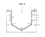
- electroless copper plating solution is used to apply electroless copper plating to a wiring structure of the interest which includes more than one opening having on a dielectric body surface an ultrafine diameter ⁇ ranging from 50 to 150 ⁇ m and a closed bottom portion deeper than such diameter, i.e. whose depth is greater in value than its width, thereby enabling fabrication of a continuous copper layer with an almost uniform thickness on or over sidewall and bottom surfaces within the opening and the dielectric body surface.
- a further feature of the invention lies in an ability to provide with increased reproducibility a multilayer wiring substrate having a microfabricated high-density wiring structure, by application to an opening having a substantially perpendicular cross-section or profile having a specified angle ⁇ the sidewall surface within the opening forms with the dielectric body surface, wherein the angle falls within a range of from 90 to 100 degrees.
- a "basic" electroless copper plating solution is the one which contains a copper salt, copper ion complexing agent, reducing agent, and pH adjuster.
- the copper salt may be presently available soluble copper salts including but not limited to copper sulfate, copper nitrate, copper chloride, and copper formate.
- Examples of the complexing agent usable in this embodiment include, inter alia,
- Examples of the reducing agent employable herein are formaldehyde, paraformaldehyde, and glyoxylic acid. Two or more materials as selected therefrom may also be used in combination when the need arises.
- pH adjuster examples include alkali hydroxides such as lithium hydroxide, sodium hydroxide and potassium hydroxide, and organic alkali such as
- the additive agent used in this embodiment for improvement of mechanical characteristics of resultant plated film and the stability of plating solution may include
- the electroless copper plating solution merely consisting of the above-noted basic components and additive agent(s)
- the uniformity of copper plated film thickness on the inside wall and bottom surfaces of via-holes is variable with changes in via-hole shape, plating solution's stirring condition, plating solution temperature, plating rate, and plating solution's main components.
- the uniformity of deposition or "precipitation" to via-holes decreases because of the fact that the copper ions (complex) and reducing agent plus hydroxides ⁇ these are main components for plating reaction ⁇ decrease in concentration at certain portions such as inside of bottom-closed via-holes whereat the plating solution used fails to offer sufficient convection current.
- the inventors of the present invention have carefully studied such various factors to find that the uniformity of deposition to via-hole inner wall surfaces greatly decreases in cases where the reducing agent concentration becomes deficient, in particular.
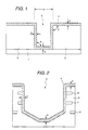
- FIG. 1 pictorially illustrates, in cross-section, main part of a substrate having a via-hole 3.
- reference numeral "1" is used to designate an underlying or "undercoat” substrate made of a chosen electrical insulative or dielectric material;
- numeral 2 denotes a dielectric layer formed thereon;
- 3 indicates an opening such as a via-hole or the like, which has a diameter ⁇ with its bottom surface being closed;
- 4 is a copper plate layer deposited.
- a thickness ratio "b/a” is defined as expressed in percentage (%). Based on this ratio b/a, the deposition uniformity has been evaluated. In case the deposition uniformity stays good, the ratio is nearly equal to 100%; if the former is bad then the latter becomes almost 0 % in value.
- Our evaluation was done by using for example a method having the steps of cutting a specified portion including the via-hole of interest away from a wiring substrate, embedding it into a chosen resin material, polishing the resulting body for causing exposure of a cross-section or profile at right angles to a diameter direction at the center of such via-hole, removing residual irregular polished portions of a copper plate film by use of soft etching techniques to thereby obtain the structure shown in Fig. 1, and then observing it by microscope equipment.
- the electroless copper plating solution further contains therein at least one of mandelonitrile and triethyltetramine in addition to the above-stated basic components thereof ⁇ i.e. the copper salt, copper ion complexing agent, reducing agent, and pH adjuster stated supra ⁇ to thereby enable fabrication of a uniform plated film at a via-hole of high aspect ratios.
- mandelonitrile and triethyltetramine in addition to the above-stated basic components thereof ⁇ i.e. the copper salt, copper ion complexing agent, reducing agent, and pH adjuster stated supra ⁇ to thereby enable fabrication of a uniform plated film at a via-hole of high aspect ratios.
- mandelonitrile and/or triethyltetramine to the basic components of the electroless copper plating solution makes it possible to improve the deposition uniformity, resulting in demonstrable improvement of via-hole interconnection reliability of build-up substrates having via-hole structures.
- plating rate is represented by a thickness of copper deposited on a unit area after elapse of a unit time, usually expressed in micrometers per hour ( ⁇ m/h).
- the inventors have found out that the shortage of the reducing agent within via-holes can cause reduction of the uniformity of deposition to via-hole inner wall surfaces, it is further found that the mandelonitrile and/or triethyltetramine as newly added may also serve to compensate for such reducing agent shortage within the via-holes concerned.
- suffix " (ad) " is used to indicate that a reactive intermediate material with this suffix added thereto has been adsorbed onto the surface of a target plating body of interest.
- a specific reactive intermediate represented as “CHOHO - (ad) " as found in reaction formulas (3) and (4) behaves to activate deposition reaction of copper, which may be local cathode reaction during plating reaction. This has been studied by Harm Wiese et al. and disclosed in Ber. Bunsenges. Phys. Chem. 91, pp. 619-626 (1987).
- a decrease in formaldehyde concentration results not only in a decrease in plating rates due to reduction of concentration of formaldehyde for use as an electron supplier, but also in a decreaae of concentration of the reactive intermediate which is adsorbed on the surface to activate the copper deposition reaction.
- the resultant plating rate at part whereat the formaldehyde concentration has decreased tends to noticeably decrease when compared to plating rates at other portions with significant formaldehyde concentration values.
- the plating deposition amount within via-holes less in formaldehyde concentration becomes much smaller than those on substrate surfaces having large formaldehyde concentrations, resulting in a likewise decrease in uniformity of deposition to inside of via-holes.
- This can be said because not only differences of local formaldehyde concentrations within via-holes and on surfaces thereof but also differences of the adsorption amount of formaldehyde reaction intermediate thereonto would serve to accelerate reduction of the deposition uniformity.
- any possible influence of the above-noted formaldehyde reaction intermediate concentration reduction may be suppressed by additional mixture of mandelonitrile and/or triethyltetramine to the electroless copper plating solution used.
- mandelonitrile and triethyltetramine per se behave to adsorb on target surfaces being plated and then mutually react with other formaldehyde reactive intermediates that have also been adsorbed thereon.
- Another cause considered is mutual reaction between such surface-adsorbed mandelonitrile/triethyltetramine and copper ions involved.
- the above is considered to be the function mechanism for improvement in the uniformity of deposition to inside of via-holes in the event that mandelonitrile and triethyltetramine are additionally mixed into the plating solution used.
- plated films are improved in mechanical characteristics upon additional mixture of at least one of 2,2'-bipyridyl, 1,10-phenanthroline and 2,9-dimethyl-1,10-phenanthroline into the electroless copper plating solution; similarly, plated film extensibilities are also improved by addition of 2,2'-bipyridyl, 1,10-phenanthroline and/or 2,9-dimethyl-1,10-phenanthroline in the case of co-use of eriochrome black T also.
- addition of at least one of 2,2'-bipyridyl, 1,10-phenanthroline and 2,9-dimethyl-1,10-phenanthroline results in an improvement in plated film's mechanical properties, particularly extensibilities thereof, thus permitting resultant plated films to become resiliency-rich ones.
- adding at least one of 2,2'-bipyridyl, 1,10-phenanthroline and 2,9-dimethyl-1,10-phenanthroline to an electroless copper plating solution that contains at least one of mandelonitrile, triethyltetramine and eriochrome black T makes it possible to improve mechanical physical properties of the resulting plated film while at the same time letting a wiring substrate with via-hole interconnections completed using this plating solution offer significantly superior via-hole interconnection reliability.
- a further effect of the present invention being presently found is that addition of at least one of 2,2'-bipyridyl, 1,10-phenanthroline and 2,9-dimethyl-1,10-phenanthroline to the electroless copper plating solution containing at least one of mandelonitrile and triethyltetramine as mixed thereinto results in a further improvement in uniformity of deposition to via-holes concerned.
- the resultant deposition uniformity improves more significantly than the case of sole use, resulting in further improvement of mechanical physical properties of plated films thus fabricated.
- the intended plated film which is excellent in uniformity of deposition to via-holes is obtainable by addition of mandelonitrile and/or triethyltetramine to the electroless copper plating solution. Similar results may also be obtained by addition of mandelonitrile, triethyltetramine and/or eriochrome black T to the electroless copper plating solution with at least one of 2,2'-bipyridyl, 1,10-phenanthroline and 2,9-dimethyl-1,10-phenanthroline being added thereto.
- a wiring substrate with wiring leads including via-hole interconnections as fabricated by use of the plating solution containing therein mandelonitrile and/or triethyltetramine or alternatively at least one of 2,2'-bipyridyl, 1,10-phenanthroline and 2,9-dimethyl-1,10-phenanthroline along with mandelonitrile, triethyltetramine and/or eriochrome black T advantageously offers excellent connection reliability.
- the use of the electroless copper plating solution incorporating the principles of this invention ensures establishment of uniform deposition of a plated film onto a via-hole with its one side closed, i.e. the one having a bottom portion, resulting in an increase in reliability of electrical connection to conductors such as wiring layers or else.
- the invention may also be applied to wiring substrates with ultrafine or "micro" via-holes while simultaneously much improving the degree of freedom or flexibility of substrate wiring designs, when compared to prior art schemes.
- a method for manufacturing a multilayer wiring substrate of the build-up type including the steps of forming a dielectric layer on or over an underlying "undercoat" substrate having a wiring layer, forming in this dielectric layer more than one via-hole deep enough to reach the wiring layer on the surface of the substrate, applying electroless copper plating to at least part of the dielectric layer surface including inner wall faces of the via-hole to thereby form a second conductive layer, and forming a wiring lead pattern on or over said dielectric layer surface, wherein via-hole plating is done by use of a specific electroless copper plating solution containing at least one of mandelonitrile and triethyltetramine as mixed thereinto for use as additive agent, has an advantage as to the capability to obtain any intended wiring substrate which is excellent in electrical interconnection reliability.
- the electroless copper plating solution is replaceable by the one that contains as additives at least one of 2,2'-bipyridyl, 1,10-phenanthroline and 2,9-dimethyl-1,10-phenanthroline with any one of mandelonitrile, triethyltetramine and eriochrome black T being further added thereto.
- a significant advantage of the wiring substrate manufacturing method lies in its demonstrable ability to improve wiring substrate manufacturing throughputs. This can be said because a time taken to perform plating processes can be shortened owing to the use of such plating solution excellent in uniformity of deposition to via-holes. This is due to the fact that although a plated film being deposited within a via-hole should be required to increase in thickness in order to provide the required connection reliability of the wiring substrate, the electroless copper plating solution designed for use with the wiring substrate manufacturing method of this invention is more excellent in uniformity of deposition to via-holes than prior known ones so that via-hole plating processing required for achievement of higher reliability may be completed with a shortened plating time period as compared to prior art methods.
- composition of a plating liquid or solution along with several plating process conditions.
- a copper-bonded glass epoxy substrate having on its surface a copper foil with a thickness of 18 ⁇ m was prepared.
- a layer of photosensitive resist was then formed on the substrate surface.
- an inner layer copper circuit was formed by etching techniques. After peel-off of the resist, the inner layer copper circuit was subjected to blackening processing for making the surface rough.
- a chosen epoxy resin film, APL-4001 commercially available from Sumitomo Bakelite Co. which has on its surface a copper foil with a thickness of 12 ⁇ m, was thermally adhered onto the glass epoxy substrate at 150°C for thirty minutes. This film measures 80 ⁇ m in thickness.
- via-holes with various diameters of ⁇ 60 ⁇ m, ⁇ 80 ⁇ m, ⁇ 100 ⁇ m, ⁇ 120 ⁇ m and ⁇ 140 ⁇ m.
- the pitch of these via-holes was set at 500 ⁇ m, resulting in formation of 2,000 holes with respective dimensions in a square substrate of 100 mm long in each side.
- desmear processing was performed by known methods using a permanganic alkali aqueous solution, followed by washing of the resulting substrate surface. Thereafter, a chosen plating catalyst processing liquid, e.g. HS-101 manufactured by Hitachi Kasei Kougyo Sha, was used to add catalyst through standard processes; then, electroless copper plating was effectuated to a thickness of about 1 ⁇ m, by using a thin-add electroless copper plating solution, e.g. CAST-2000 available from Hitachi Kasei Kougyo Sha. Next, backing was done at 160 °C for one hour, thus completing the test substrate.
- a chosen plating catalyst processing liquid e.g. HS-101 manufactured by Hitachi Kasei Kougyo Sha
- electroless copper plating was effectuated to a thickness of about 1 ⁇ m, by using a thin-add electroless copper plating solution, e.g. CAST-2000 available from Hitachi Kasei Kougyo Sha.
- backing was done at
- a plated film used for measurement of physical properties (mechanical characteristics of plated film) as used herein is the one with a thickness of 30 ⁇ m as formed on a stainless plate.
- This plate is the one that has fabricated through the process steps of pre-immersion into a 17-% hydrochloric acid aqueous solution for two minutes, immersion into a single-fluid palladium colloid catalyzer solution (acidified aqueous solution containing a sensitizer HS101B from Hitachi Kasei Kougyo Kabushiki Kaisha) for 10 minutes, water washing, processing by a chosen accelerating agent with diluted hydrochloric acid being as its main component for 5 minutes, and water washing again.
- the plating solution was stirred while letting flesh air be introduced constantly.
- supplementary feed was done to ensure that any one of the copper ions and copper ion reducing agent are kept constant in concentration while simultaneously causing the pH value to stay at a specified level.
- the percentage of a plated film thickness at the via-hole bottom portion of each diameter relative to the thickness value, 24.9 ⁇ m, of a plated film on the substrate surface represents the deposition uniformity.
- the deposition uniformity was as follows: 68% for a via-hole of ⁇ 60 ⁇ m, 77% for a via-hole of ⁇ 80 ⁇ m, 89% for a via-hole of ⁇ 100 ⁇ m, 96% for a via-hole of ⁇ 120 ⁇ m, and 100% for a via-hole of ⁇ 140 ⁇ m, wherein excellent deposition uniformity was obtained in each case irrespective of the fact that the plating rate is set as high as 8.3 ⁇ m/h.
- the physical properties of the plated film obtained using the plating solution under the plating conditions of this embodiment have been evaluated. This evaluation was done by a process having the steps of pealing a plated coat film off from the stainless plate, cutting it into portions each having a size of 1.25 cm ⁇ 10 cm, and then measuring the mechanical strength of such plated coat film by using a standard tension testing machine. As a result, the plated coat film's rate of elongation or "extensibility" was at 3.2%. This is a sufficient level of plated film physical property for provision of the intended connection reliability of a build-up substrate.
- the electroless copper plating solution which contains therein mandelonitrile as additive agent is excellent in uniformity of deposition onto via-holes, convincing the presence of effects of the invention.
- the plated film's physical properties are at a level high enough to permit achievement of the intended build-up substrate connection reliability; thus, it has been affirmed that the wiring substrate manufacturing method using the electroless copper plating solution shown in this embodiment is suitable for use as a method of manufacturing build-up substrates having via-hole connection structures, leading to affirmance of effects of this example.
- composition of a plating solution used in this embodiment along with plating process conditions.
- the deposition uniformity and plated film's physical properties were evaluated by using a test substrate and method for fabricating a physical property measuring plated film plus deposition uniformity evaluation method, all of which are similar to those in Embodiment 1 stated above.
- the resultant plating rate with use of the plating solution of this embodiment was 5.5 ⁇ m/h.
- Plating was applied to the top surface of the test substrate for 4.5 hours, thereby forming a plated film with a thickness of about 25 ⁇ m.
- Evaluation results of the deposition uniformity are as follows: 92% for a via-hole of ⁇ 60 ⁇ m, 99% for a via-hole of ⁇ 80 ⁇ m, and 100% for via-holes of ⁇ 100 ⁇ m, ⁇ 120 ⁇ m and ⁇ 140 ⁇ m. Excellent deposition uniformity was obtained irrespective of the fact that the plating rate is as high as 5.5 ⁇ m/h.
- the physical properties of the plated film obtained using the plating solution and the plating conditions of this embodiment were evaluated.
- the plated film's rate of elongation or extensibility was 3.8%. This is a sufficient level of plated film physical property for achievement of the intended connection reliability of a build-up substrate.
- the electroless copper plating solution containing therein triethyltetramine as additive agent is excellent in uniformity of deposition onto via-holes, convincing the presence of effects of the invention.
- the plated film's physical properties are at a level high enough to permit achievement of the intended build-up substrate connection reliability; thus, it has been affirmed that the wiring substrate manufacturing method using the electroless copper plating solution shown in this embodiment is suitable for use as a method of manufacturing build-up substrates having via-hole connection structures, leading to affirmance of effects of this embodiment.
- the deposition uniformity and plated film's physical properties were evaluated by using a test substrate and method for fabricating a physical property measuring plated film plus deposition uniformity evaluation method, all of which are similar to those in Embodiment 1 stated above.
- the resultant plating rate with use of the plating solution of this embodiment was 4.3 ⁇ m/h.
- Plating was applied to the top surface of the test substrate for 6 hours, thereby forming a plated film with a thickness of about 26 ⁇ m.
- Evaluation results of the deposition uniformity are as follows: 100% for all the via-holes of ⁇ 60 ⁇ m to ⁇ 140 ⁇ m. Excellent deposition uniformity was obtained irrespective of the fact that the plating rate is as high as 4.3 ⁇ m/h.
- the physical properties of the plated film obtained using the plating solution and the plating conditions of this embodiment were evaluated.
- the plated film's extensibility was 3.4%. This is a sufficient level of plated film physical property for achievement of the intended connection reliability of a build-up substrate.
- the electroless copper plating solution containing therein triethyltetramine as additive agent is excellent in uniformity of deposition onto via-holes, convincing the presence of effects of the invention.
- the plated film's physical properties are at a level high enough to permit achievement of the intended build-up substrate connection reliability; thus, it has been affirmed that the wiring substrate manufacturing method using the electroless.copper plating solution shown in this embodiment is suitable for use as a method of manufacturing build-up substrates having via-hole connection structures, leading to affirmance of effects of this embodiment.
- the deposition uniformity and plated film's physical properties were evaluated by using a test substrate and method for fabricating a physical property measuring plated film plus deposition uniformity evaluation method, all of which are similar to those in Embodiment 1 stated above.
- the resultant plating rate with use of the plating solution of this embodiment was 5.1 ⁇ m/h.
- Plating was applied to the top surface of the test substrate for 5 hours, thereby forming a plated film with a thickness of about 25.5 ⁇ m.
- Evaluation results of the deposition uniformity are as follows: 90% for a via-hole of ⁇ 60 ⁇ m, 99% for a via-hole of ⁇ 80 ⁇ m, and 100% for via-holes of ⁇ 100 ⁇ m, ⁇ 120 ⁇ m and ⁇ 140 ⁇ m. Excellent deposition uniformity was obtained irrespective of the fact that the plating rate is as high as 5.1 ⁇ m/h.
- the physical properties of the plated film obtained using the plating solution and the plating conditions of this embodiment were evaluated.
- the plated film's extensibility was 15.3%. This is a sufficient level of plated film physical property for achievement of the intended connection reliability of a build-up substrate.
- the electroless copper plating solution containing therein mandelonitrile as additive agent is excellent in uniformity of deposition to via-holes, convincing the presence of effects of this embodiment.
- the co-use with 2,2'-bipyridyl results in the plated film's physical properties becoming demonstrably excellent, which well demonstrates the presence of an ability to achieve sufficiently high connection reliability of a build-up substrate manufactured.
- the wiring substrate manufacturing method employing the electroless copper plating solution shown herein is suitable for use as a method of manufacturing build-up substrates having via-hole connection structures, leading to affirmance of effects of this embodiment.
- composition of a plating solution used in this embodiment along with plating process conditions.
- the deposition uniformity and plated film's physical properties were evaluated by using a test substrate and method for fabricating a physical property measuring plated film plus deposition uniformity evaluation method, all of which are similar to those in Embodiment 1 stated above.
- the resultant plating rate with use of the plating solution of this embodiment was 4.8 ⁇ m/h.
- Plating was applied to the top surface of the test substrate for 5 hours, thereby forming a plated film with a thickness of about 24 ⁇ m.
- Evaluation results of the deposition uniformity are as follows: 97% for a via-hole of ⁇ 60 ⁇ m, and 100% for all the via-holes of ⁇ 80 ⁇ m to ⁇ 140 ⁇ m. Good deposition uniformity was obtained irrespective of the fact that the plating rate is as high as 4.8 ⁇ m/h.
- the physical properties of the plated film obtained using the plating solution and the plating conditions of this embodiment were evaluated.
- the plated film's rate of elongation or extensibility was 7.8%. This is a sufficient level of plated film physical property for achievement of the intended connection reliability of a build-up substrate.
- the electroless copper plating solution containing therein triethyltetramine as additive agent is excellent in uniformity of deposition to via-holes, convincing the presence of effects of this embodiment.
- the co-use with 2,2'-bipyridyl results in the plated film's physical properties becoming demonstrably excellent, which well demonstrates the presence of an ability to achieve sufficiently high connection reliability of a build-up substrate manufactured.
- the wiring substrate manufacturing method employing the electroless copper plating solution shown herein is suitable for use as a method of manufacturing build-up substrates having via-hole connection structures, leading to affirmance of effects of this embodiment.
- the deposition uniformity and plated film's physical properties were evaluated by using a test substrate and method for fabricating a physical property measuring plated film plus deposition uniformity evaluation method, all of which are similar to those in Embodiment 1.
- the resultant plating rate with use of the plating solution of this embodiment was 5.8 ⁇ m/h.
- Plating was applied to the top surface of the test substrate for 4.5 hours, thereby forming a plated film with a thickness of about 26 ⁇ m.
- Evaluation results of the deposition uniformity are as follows: 100% for all the via-holes of from ⁇ 60 ⁇ m to ⁇ 140 ⁇ m. Good deposition uniformity was obtained irrespective of the fact that the plating rate is as high as 5.8 ⁇ m/h.
- the physical properties of the plated film obtained using the plating solution and the plating conditions of this embodiment were evaluated.
- the plated film's rate of elongation or extensibility was 8.5%. This is a sufficient level of plated film physical property for achievement of the intended connection reliability of a build-up substrate.
- the electroless copper plating solution containing therein eriochrome black T and 2,2'-bipyridyl as additive agents is excellent in uniformity of deposition to via-holes, convincing the presence of effects of this embodiment. Further, the plated film's physical properties also are excellent, which suggests that it is possible to achieve sufficiently high connection reliability of a build-up substrate.
- the wiring substrate manufacturing method using the electroless copper plating solution shown in this embodiment is suitable for use as a method of manufacturing build-up substrates having via-hole connection structures, leading to affirmance of effects of this embodiment.
- the deposition uniformity and plated film's physical properties were evaluated by using a test substrate and method for fabricating a physical property measuring plated film plus deposition uniformity evaluation method, all of which are similar to those in Embodiment 1.
- the resultant plating rate with use of the plating solution of this embodiment was 6.0 ⁇ m/h.
- Plating was applied to the top surface of the test substrate for 4 hours, thereby forming a plated film with a thickness of about 24 ⁇ m.
- Evaluation results of the deposition uniformity are as follows: 100% for all the via-holes of from ⁇ 60 ⁇ m to ⁇ 140 ⁇ m. Good deposition uniformity was obtained irrespective of the fact that the plating rate is as high as 6.0 ⁇ m/h.
- the physical properties of the plated film obtained using the plating solution and the plating conditions of this embodiment were evaluated.
- the plated film's extensibility was as good as 7.6%. This is a sufficient level of plated film physical property for achievement of the intended connection reliability of a build-up substrate.
- the electroless.copper plating solution containing therein eriochrome black T and 2,2'-bipyridyl as additive agents is excellent in uniformity of deposition to via-holes, convincing the presence of effects of this embodiment. Further, the plated film's physical properties also are excellent, which suggests that it is possible to achieve sufficiently high connection reliability of a build-up substrate.
- the wiring substrate manufacturing method using the electroless copper plating solution shown in this embodiment is suitable for use as a method of manufacturing build-up substrates having via-hole connection structures, leading to affirmance of effects of this embodiment.
- the deposition uniformity and plated film's physical properties were evaluated by using a test substrate and method for fabricating a physical property measuring plated film plus deposition uniformity evaluation method, all of which are similar to those in Embodiment 1.
- the resultant plating rate with use of the plating solution of this embodiment was 4.7 ⁇ m/h.
- Plating was applied to the top surface of the test substrate for 5.5 hours, thereby forming a plated film with a thickness of about 26 ⁇ m.
- Evaluation results of the deposition uniformity are as follows: 100% for all the via-holes of from ⁇ 60 ⁇ m to ⁇ 140 ⁇ m. Good deposition uniformity was obtained irrespective of the fact that the plating rate is as high as 4.7 ⁇ m/h.
- the physical properties of the plated film obtained using the plating solution and the plating conditions of this embodiment were evaluated.
- the plated film's extensibility was as good as 9.6%. This is a sufficient level of plated film physical property for achievement of the intended connection reliability of a build-up substrate.
- the electroless copper plating solution containing therein eriochrome black T and 2,2'-bipyridyl as additive agents is excellent in uniformity of deposition to via-holes, convincing the presence of effects of this embodiment. Further, the plated film's physical properties also are excellent, which indicates that it is possible to achieve sufficiently high connection reliability of a build-up substrate.
- the wiring substrate manufacturing method using the electroless copper plating solution shown in this embodiment is suitable for use as a method of manufacturing build-up substrates having via-hole connection structures, leading to affirmance of effects of this embodiment.
- the deposition uniformity and plated film's physical properties were evaluated by using a test substrate and method for fabricating a physical property measuring plated film plus deposition uniformity evaluation method, all of which are similar to those in Embodiment 1.
- the resultant plating rate with use of the plating solution of this embodiment was 7.6 ⁇ m/h.
- Plating was applied to the top surface of the test substrate for 3.3 hours, thereby forming a plated film with a thickness of about 25 ⁇ m.
- Evaluation results of the deposition uniformity are as follows: 72% for a via-hole of ⁇ 60 ⁇ m, 79% for a via-hole of ⁇ 80 ⁇ m, 93% for a via-hole of ⁇ 100 ⁇ m, and 100% for via-holes of ⁇ 120 ⁇ m and ⁇ 140 ⁇ m. Good deposition uniformity was obtained irrespective of the fact that the plating rate is as high as 7.6 ⁇ m/h.
- the physical properties of the plated film obtained using the plating solution and the plating conditions of this embodiment were evaluated.
- the plated film's extensibility was as good as 7.6%. This is a sufficient level of plated film physical property for achievement of the intended connection reliability of a build-up substrate.
- the electroless copper plating solution containing therein mandelonitrile and polyethylene glycol as additive agents is excellent in uniformity of deposition to via-holes, convincing the presence of effects of this embodiment. Further, the plated film's physical properties also are excellent, which suggests that it is possible to achieve sufficiently high connection reliability of a build-up substrate.
- the wiring substrate manufacturing method using the electroless copper plating solution shown in this embodiment is suitable for use as a method of manufacturing build-up substrates having via-hole connection structures, leading to affirmance of effects of this embodiment.
- the deposition uniformity and plated film's physical properties were evaluated by using a test substrate and method for fabricating a physical property measuring plated film plus deposition uniformity evaluation method, all of which are similar to those in Embodiment 1.
- the resultant plating rate with use of the plating solution of this embodiment was 4.9 ⁇ m/h.
- Plating was applied to the top surface of the test substrate for 5 hours, thereby forming a plated film with a thickness of about 25 ⁇ m.
- Evaluation results of the deposition uniformity are as follows: 100% for all the via-holes of from ⁇ 60 ⁇ m to ⁇ 140 ⁇ m. Good deposition uniformity was obtained irrespective of the fact that the plating rate is as high as 4.9 ⁇ m/h.
- the physical properties of the plated film obtained using the plating solution and the plating conditions of this embodiment were evaluated.
- the plated film's extensibility was as good as 6.8%. This is a sufficient level of plated film physical property for achievement of the intended connection reliability of a build-up substrate. From the foregoing, it has been affirmed that the electroless copper plating solution containing therein triethyltetramine and polyethylene glycol as additive agents is excellent in uniformity of deposition to via-holes, convincing the presence of effects of this embodiment. Further, the plated film's physical properties also are excellent, which suggests that it is possible to achieve sufficiently high connection reliability of a build-up substrate.
- the wiring substrate manufacturing method using the electroless copper plating solution shown in this embodiment is suitable for use as a method of manufacturing build-up substrates having via-hole connection structures, leading to affirmance of effects of this embodiment.
- the deposition uniformity and plated film's physical properties were evaluated by using a test substrate and method for fabricating a physical property measuring plated film plus deposition uniformity evaluation method, all of which are similar to those in Embodiment 1.
- the resultant plating rate with use of the plating solution of this embodiment was 7.5 ⁇ m/h.
- Plating was applied to the top surface of the test substrate for 3.5 hours, thereby forming a plated film with a thickness of about 26 ⁇ m.
- Evaluation results of the deposition uniformity are as follows: 75% for a via-hole of ⁇ 60 ⁇ m, 83% for a via-hole of ⁇ 80 ⁇ m, 96% for a via-hole of ⁇ 100 ⁇ m, and 100% for via-holes of ⁇ 120 ⁇ m and ⁇ 140 ⁇ m. Good deposition uniformity was obtained irrespective of the fact that the plating rate is as high as 7.5 ⁇ m/h.
- the physical properties of the plated film obtained using the plating solution and the plating conditions of this embodiment were evaluated.
- the plated film's extensibility was as good as 5.4%. This is a sufficient level of plated film physical property for achievement of the intended connection reliability of a build-up substrate.
- the electroless copper plating solution containing therein eriochrome black T and polyethylene glycol as additive agents is excellent in uniformity of deposition to via-holes, convincing the presence of effects of this embodiment. Further, the plated film's physical properties also are excellent, which suggests that it is possible to achieve sufficiently high connection reliability of a build-up substrate.
- the wiring substrate manufacturing method using the electroless copper plating solution shown in this embodiment is suitable for use as a method of manufacturing build-up substrates having via-hole connection structures, leading to affirmance of effects of this embodiment.
- the deposition uniformity and plated film's physical properties were evaluated by using a test substrate and method for fabricating a physical property measuring plated film plus deposition uniformity evaluation method, all of which are similar to those in Embodiment 1.
- the resultant plating rate with use of the plating solution of this embodiment was 6.7 ⁇ m/h.
- Plating was applied to the top surface of the test substrate for 4.0 hours, thereby forming a plated film with a thickness of about 27 ⁇ m.
- Evaluation results of the deposition uniformity are as follows: 77% for a via-hole of ⁇ 60 ⁇ m, 88% for a via-hole of ⁇ 80 ⁇ m, 96% for avia-hole of ⁇ 100 ⁇ m, and 100% for via-holes of ⁇ 120 ⁇ m and ⁇ 140 ⁇ m. Good deposition uniformity was obtained irrespective of the fact that the plating rate is as high as 6.7 ⁇ m/h.
- the physical properties of the plated film obtained using the plating solution and the plating conditions of this embodiment were evaluated.
- the plated film's extensibility was as good as 5.2%. This is a sufficient level of plated film physical property for achievement of the intended connection reliability of a build-up substrate.
- the electroless copper plating solution containing therein eriochrome black T and 2,9-dimethyl-1,10-phenanthroline as additive agents is excellent in uniformity of deposition to via-holes, convincing the presence of effects of this embodiment. Further, the plated film's physical properties also are excellent, which suggests that it is possible to achieve sufficiently high connection reliability of a build-up substrate.
- the wiring substrate manufacturing method using the electroless copper plating solution shown in this embodiment is suitable for use as a method of manufacturing build-up substrates having via-hole connection structures, leading to affirmance of effects of this example.
- the deposition uniformity and plated film's physical properties were evaluated by using a test substrate and method for fabricating a physical property measuring plated film plus deposition uniformity evaluation method, all of which are similar to those in Embodiment 1.
- the resultant plating rate with use of the plating solution of this embodiment was 5.3 ⁇ m/h.
- Plating was applied to the top surface of the test substrate for 5.0 hours, thereby forming a plated film with a thickness of about 26 ⁇ m.
- Evaluation results of the deposition uniformity are as follows: 91% for a via-hole of ⁇ 60 ⁇ m, and 100% for via-holes of ⁇ 80 ⁇ m, ⁇ 100 ⁇ m, ⁇ 120 ⁇ m and ⁇ 140 ⁇ m. Good deposition uniformity was obtained irrespective of the fact that the plating rate is as high as 5.3 ⁇ m/h.
- the physical properties of the plated film obtained using the plating solution and the plating conditions of this embodiment were evaluated.
- the plated film's extensibility was as good as 6.8%. This is a sufficient level of plated film physical property for achievement of the intended connection reliability of a build-up substrate.
- the electroless copper plating solution containing therein mandelonitrile and 2,9-dimethyl-1,10-phenanthroline as additive agents is excellent in uniformity of deposition to via-holes, convincing the presence of effects of this embodiment. Further, the plated film's physical properties also are excellent, which suggests that it is possible to achieve sufficiently high connection reliability of a build-up substrate.
- the wiring substrate manufacturing method using the electroless copper plating solution shown in this embodiment is suitable for use as a method of manufacturing build-up substrates having via-hole connection structures, leading to affirmance of effects of this example.
- the deposition uniformity and plated film's physical properties were evaluated by using a test substrate and method for fabricating a physical property measuring plated film plus deposition uniformity evaluation method, all of which are similar to those in Embodiment 1.
- the resultant plating rate with use of the plating solution of this embodiment was 4.9 ⁇ m/h.
- Plating was applied to the top surface of the test substrate for 5.0 hours, thereby forming a plated film with a thickness of about 25 ⁇ m.
- Evaluation results of the deposition uniformity are as follows: 92% for a via-hole of ⁇ 60 ⁇ m, and 100% for via-holes of ⁇ 80 ⁇ m, ⁇ 100 ⁇ m, ⁇ 120 ⁇ m and ⁇ 140 ⁇ m. Good deposition uniformity was obtained irrespective of the fact that the plating rate is as high as 4.9 ⁇ m/h.
- the physical properties of the plated film obtained using the plating solution and the plating conditions of this embodiment were evaluated.
- the plated film's extensibility was as good as 6.9%. This is a sufficient level of plated film physical property for achievement of the intended connection reliability of a build-up substrate.
- the electroless copper plating solution containing therein triethyltetramine and 2,9-dimethyl-1, 10-phenanthroline as additive agents is excellent in uniformity of deposition to via-holes, convincing the presence of effects of this embodiment. Further, the plated film's physical properties also are excellent, which suggests that it is possible to achieve sufficiently high connection reliability of a build-up substrate.
- the wiring substrate manufacturing method using the electroless copper plating solution shown in this embodiment is suitable for use as a method of manufacturing build-up substrates having via-hole connection structures, leading to affirmance of effects of this example.
- the deposition uniformity and plated film's physical properties were evaluated by using a test substrate and method for fabricating a physical property measuring plated film plus deposition uniformity evaluation method, all of which are similar to those in Embodiment 1.
- the resultant plating rate with use of the plating solution of this embodiment was 4.8 ⁇ m/h.
- Plating was applied to the top surface of the test substrate for 5 hours, thereby forming a plated film with a thickness of about 24 ⁇ m.
- Evaluation results of the deposition uniformity are as follows: 100% for all the via-holes of from ⁇ 60 ⁇ m up to ⁇ 140 ⁇ m. Good deposition uniformity was obtained irrespective of the fact that the plating rate is as high as 4.8 ⁇ m/h.
- the physical properties of the plated film obtained using the plating solution and the plating conditions of this embodiment were evaluated.
- the plated film's extensibility was 18.3% and thus significantly excellent. This is a sufficient level of plated film physical property for achievement of the intended connection reliability of a build-up substrate.
- the electroless copper plating solution containing therein mandelonitrile and polyethylene glycol plus 2,2'-bipyridyl as additive agents is excellent in uniformity of deposition to via-holes, convincing the presence of effects of this embodiment. Further, the plated film's physical properties also are excellent, which suggests that it is possible to achieve sufficiently high connection reliability of a build-up substrate.
- the wiring substrate manufacturing method using the electroless copper plating solution shown in this embodiment is suitable for use as a method of manufacturing build-up substrates having via-hole connection structures, leading to affirmance of effects of this embodiment.
- the deposition uniformity and plated film's physical properties were evaluated by using a test substrate and method for fabricating a physical property measuring plated film plus deposition uniformity evaluation method, all of which are similar to those in Embodiment 1.
- the resultant plating rate with use of the plating solution of this embodiment was 4.1 ⁇ m/h.
- Plating was applied to the top surface of the test substrate for 6 hours, thereby forming a plated film with a thickness of about 25 ⁇ m.
- Evaluation results of the deposition uniformity are as follows: 100% for all the via-holes of from ⁇ 60 ⁇ m up to ⁇ 140 ⁇ m. Good deposition uniformity was obtained irrespective of the fact that the plating rate is as high as 4.1 ⁇ m/h.
- the physical properties of the plated film obtained using the plating solution and the plating conditions of this embodiment were evaluated.
- the plated film's extensibility was at a very good value of 8.6%. This is a sufficient level of plated film physical property for achievement of the intended connection reliability of a build-up substrate.
- the electroless copper plating solution containing therein triethyltetramine and polyethylene glycol plus 2,2'-bipyridyl as additive agents is excellent in uniformity of deposition to via-holes, convincing the presence of effects of this embodiment. Further, the plated film's physical properties also are excellent, which suggests that it is possible to achieve sufficiently high connection reliability of a build-up substrate.
- the wiring substrate manufacturing method using the electroless copper plating solution shown in this embodiment is suitable for use as a method of manufacturing build-up substrates having via-hole connection structures, leading to affirmance of effects of this embodiment.
- the deposition uniformity and plated film's physical properties were evaluated by using a test substrate and method for fabricating a physical property measuring plated film plus deposition uniformity evaluation method, all of which are similar to those in Embodiment 1.
- the resultant plating rate with use of the plating solution of this embodiment was 5.9 ⁇ m/h.
- Plating was applied to the top surface of the test substrate for 4.2 hours, thereby forming a plated film with a thickness of about 25 ⁇ m.
- Evaluation results of the deposition uniformity are as follows: 100% for all the via-holes of from ⁇ 60 ⁇ m up to ⁇ 140 ⁇ m. Good deposition uniformity was obtained irrespective of the fact that the plating rate is as high as 5.9 ⁇ m/h.
- the physical properties of the plated film obtained using the plating solution and the plating conditions of this embodiment were evaluated.
- the plated film's extensibility was 8.4% and thus significantly excellent. This is a sufficient level of plated film physical property for achievement of the intended connection reliability of a build-up substrate.
- the electroless copper plating solution containing therein eriochrome black T and polyethylene glycol plus 2,2'-bipyridyl as additive agents is excellent in uniformity of deposition to via-holes, convincing the presence of effects of this embodiment. Further, the plated film's physical properties also are excellent, which suggests that it is possible to achieve sufficiently high connection reliability of a build-up substrate.
- the wiring substrate manufacturing method using the electroless copper plating solution shown in this embodiment is suitable for use as a method of manufacturing build-up substrates having via-hole connection structures, leading to affirmance of effects of this embodiment.
- the deposition uniformity and plated film's physical properties were evaluated by using a test substrate and method for fabricating a physical property measuring plated film plus deposition uniformity evaluation method, all of which are similar to those in Embodiment 1.
- the resultant plating rate with use of the plating solution of this embodiment was 4.5 ⁇ m/h.
- Plating was applied to the top surface of the test substrate for 5.5 hours, thereby forming a plated film with a thickness of about 25 ⁇ m.
- Evaluation results of the deposition uniformity are as follows: 100% for all the via-holes of from ⁇ 60 ⁇ m up to ⁇ 140 ⁇ m. Good deposition uniformity was obtained irrespective of the fact that the plating rate is as high as 4.5 ⁇ m/h.
- the physical properties of the plated film obtained using the plating solution and the plating conditions of this embodiment were evaluated.
- the plated film's extensibility was at a very excellent value of 18.6%. This is a sufficient level of plated film physical property for achievement of the intended connection reliability of a build-up substrate.
- the electroless copper plating solution containing therein mandelonitrile and polyethylene glycol plus 2,2'-bipyridyl as additive agents is excellent in uniformity of deposition to via-holes, convincing the presence of effects of this embodiment. Further, the plated film's physical properties also are excellent, which suggests that it is possible to achieve sufficiently high connection reliability of a build-up substrate.
- the wiring substrate manufacturing method using the electroless copper plating solution shown in this embodiment is suitable for use as a method of manufacturing build-up substrates having via-hole connection structures, leading to affirmance of effects of this embodiment.
- a layer of photosensitive resist material was formed on the surface of a copper-bonded glass epoxy substrate having thereon a copper foil with a thickness of 18 ⁇ m; after completion of patterning, an inner layer circuit was formed by etching techniques. This circuit measures 75 ⁇ m in width and 75 ⁇ m in space, wherein square interlayer connection pads with each side of 250 ⁇ m are formed and disposed with a pitch of 1.27 mm. After having peeled off the resist, the inner layer copper circuit surface is made coarser through blackening processes.
- An epoxy resin film APL-4001 commercially available from Sumitomo Bakelite Co., which has on its surface a copper foil with a thickness of 12 ⁇ m, was adhered by thermo-compression bonding techniques at a temperature of 150°C for 30 minutes.
- This film is 80 ⁇ m thick. Thereafter, a surface portion of the copper foil was etched away; then, a carbon dioxide gas laser manufactured by Hitachi Via Mechanics Co. was used to form a via-hole(s) of 80 ⁇ m in diameter on an interlayer connection pad(s) as formed at the inner layer. After completion of such via-hole formation, standard methodology was used to perform desmear processing using a permanganate alkaline aqueous solution; after having washed the resulting substrate surface, a plating catalytic processing liquid, e.g.
- HS-101 manufactured by Hitachi Kasei Kougyo Sha was used to add catalyst through known processes; thereafter, electroless copper plating was applied thereto using a thin-add electroless copper plating solution, here CAST-2000 also available from Hitachi Kasei Kougyo Sha. Then, backing was carried out at 160°C for one hour; next, electroless copper plating was done to a thickness of 25 ⁇ m using a chosen plating solution and plating process conditions given below.
- a photosensitive resist was formed on a copper-plated film, which was then subject to pattering.
- the pattern thus formed has its structure with a linear array of 2,500 via-holes, which structure is used for measurement of the chain resistivity of these via-holes.
- these 2,500 via-holes' chain resistance value immediately after completion of plating was measured for comparison with a resistance value at the same substrate after a thermal shock test. This test was done under the following conditions.
- thermal shock test results in that a substrate sample fabricated was such that the resistance rise-up rate exceeded 10% after elapse of 180 cycles.
- This thermal shock test result demonstrates that the substrate exhibits sufficient reliability in view of build-up substrate connection reliability evaluation results; thus it has been affirmed that the wiring substrate manufacturing method of the present invention is capable of obtaining the intended wiring substrate with excellent connection reliability.
- a substrate sample fabricated in this embodiment was such that the resistance rise-up rate exceeds 10% after elapse of 180 cycles in a similar way to that in Example 19.
- This thermal shock test result suggests that the substrate exhibits sufficient reliability in view of build-up substrate connection reliability evaluation results; thus it has been affirmed that the wiring substrate manufacturing method of the present invention is capable of obtaining the intended wiring substrate with excellent connection reliability.
- a substrate sample fabricated in this embodiment was such that the resistance rise-up rate exceeds 10% after 200 cycles, which is a slightly better result than those of Embodiments 19 and 20. It is considered that this is because addition of 2,2'-bipyridyl results in improvement of mechanical physical properties of the resulting plated film. Additionally this thermal shock test result demonstrates that the substrate exhibits sufficient reliability in view of build-up substrate connection reliability evaluation results; thus it has been affirmed that the wiring substrate manufacturing method of the present invention is capable of obtaining the intended wiring substrate with excellent connection reliability.
- a substrate sample fabricated in this embodiment was such that the resistance rise-up rate exceeds 10% after 200 cycles, which is a slightly better result than those of Embodiments 19 and 20. It is considered that this is because addition of 2,2'-bipyridyl results in improvement of mechanical physical properties of the resulting plated film. Additionally, this thermal shock test result demonstrates that the substrate exhibits sufficient reliability in view of build-up substrate connection reliability evaluation results; thus it has been affirmed that the wiring substrate manufacturing method of the present invention is capable of obtaining the intended wiring substrate with excellent connection reliability.
- a substrate sample fabricated in this embodiment was such that the resistance rise-up rate exceeds 10% after 200 cycles, which is a slightly better result than those of Examples 19 and 20. It is considered that this is because addition of 2,2'-bipyridyl results in improvement of mechanical physical properties of the resulting plated film.
- this thermal shock test result demonstrates that the substrate exhibits sufficient reliability in view of build-up substrate connection reliability evaluation results; thus it has been affirmed also in the case of employing glyoxylic acid as the required reducing agent that the wiring substrate manufacturing method of the present invention is capable of obtaining the intended wiring substrate with excellent connection reliability.
- the plating solution contains no additive agents. Its deposition uniformity and plated film's physical properties have been evaluated by use of a test substrate, physical property measurement plated film fabrication method and deposition uniformity evaluation method, all of which are the same as those of Embodiment 1.
- the plating rate was measured to be 15.8 ⁇ m/h. After applying plating to the top surface of test substrate for 1.5 hours, a plated film was formed to a thickness of about 24 ⁇ m.
- each via-hole was observed to thereby find that no plated film components are deposited within via-holes and also that deposition characteristics are at almost 0% with respect to all the via-holes concerned, including ⁇ 60 ⁇ m via-holes up to ⁇ 140 ⁇ m ones.
- the resultant plated film thus obtained using the plating solution under the plating conditions of the comparative example was very crumbly: our physical property evaluation results indicate that the degree of extensibility was as less as 0.3%.
- the plating solution was undesirably decomposed after completion of plating processing for 2 hours, resulting in copper components being deposited on wall surfaces of a plating bath used.
- the plating solution of this comparative example containing therein no additive agents is less or "bad" in deposition uniformity. Accordingly it could be affirmed that the plating solution of the present invention containing mandelonitrile, triethyltetramine and/or eriochrome black T as stated previously is excellent in deposition uniformity, thus proving the presence of effects of the plating solution of the invention. Additionally the wiring substrate manufacturing method using the electroless copper plating solution of the above-noted comparative example is bad in uniformity of deposition to via-holes and also bad in mechanical characteristics of resultant plated film, which makes it impossible to provide any required wiring substrate reliability, and thus is not preferable in any way. From this fact also, it could be made sure that the manufacturing method of the invention is very effective for use as wiring substrate manufacturing methodology, which is an advantage unique to the invention.
- composition and plating conditions of a plating solution that was used in another example for comparison will be given below.
- This comparative example is such that while 2,2'-bipyridyl is contained as additive agent in a plating solution, this solution contains none of mandelonitrile, triethyltetramine and eriochrome black T which are for use as the additive agents in order to improve the uniformity of deposition to via-holes.
- the deposition uniformity and plated film's physical properties thereof have been evaluated by use of a test substrate, physical property measurement plated film fabrication method and deposition uniformity evaluation method which are the same as those of Embodiment 1.
- the plating rate was 5.5 ⁇ m/h.
- Deposition uniformity measurement results are as follows: 25% for ⁇ 60 ⁇ m via-holes, 30% for ⁇ 80 ⁇ m via-holes, 57% for ⁇ 100 ⁇ m via-holes, 67% for ⁇ 120 ⁇ m via-holes, and 87% for ⁇ 140 ⁇ m via-holes. This suggests that the to-the-via-hole deposition uniformities are unacceptably inferior when compared to the samples of the invention that exhibit similar plating rates.
- the plating solution of the comparative example containing therein none of the additive agents with effects for improving the deposition uniformity is bad in deposition uniformity. Accordingly it could be affirmed that the plating solution of the present invention containing mandelonitrile, triethyltetramine and/or eriochrome black T is excellent in deposition uniformity, thus convincing the presence of effects of the plating solution of the invention. Additionally the wiring substrate manufacturing method using the electroless copper plating solution of the above-noted comparative example is bad in uniformity of deposition to via-holes, which makes it impossible to achieve any required wiring substrate reliability, and thus is not preferable in any way. From this fact also, it could be made sure that the manufacturing method of the invention is very effective for use as wiring substrate manufacturing methodology, which is an advantage unique to the invention.
- composition and plating conditions of a plating solution that was used in yet another comparative example will be shown below.
- This comparative example is such that its plating solution contains therein eriochrome black T alone.
- the deposition uniformity and plated film' s physical properties thereof have been evaluated by use of a test substrate, physical property measurement plated film fabrication method and deposition uniformity evaluation method, which are the same as those of Embodiment 1.
- the plating rate was measured to be 10.4 ⁇ m/h. After applying plating to the test substrate top surface for 2.4 hours, a plated film was formed to a thickness of about 25 ⁇ m.
- Precipitation uniformity measurement results are as follows: 18% for ⁇ 60 ⁇ m via-holes, 25% for ⁇ 80 ⁇ m via-holes, 33% for ⁇ 100 ⁇ m via-holes, 48% for ⁇ 120 ⁇ m via-holes, and 60% for ⁇ 140 ⁇ m via-holes. This suggests that the to-the-via-hole deposition uniformities are unacceptably less when compared to the embodiments of the invention containing 2,2'-bipyridyl and/or polyalkylene glycol.
- the electroless copper plating solution of the comparative example with only eriochrome black T being mixed into the plating liquid is bad in deposition uniformity.
- the electroless copper plating solution of the present invention is excellent in precipitation uniformity, thus convincing the presence of effects of the plating solution of the invention.
- the wiring substrate manufacturing method using the electroless copper plating solution of the above-noted comparative example is bad in uniformity of deposition to via-holes, which makes it impossible to achieve any required wiring substrate reliability, and thus is not preferable in any way. From this fact also, it could be made sure that the manufacturing method of the invention is very effective for use as wiring substrate manufacturing methodology, which is an advantage unique to the invention.
- the opening 3 has its diameter ⁇ ranging in value from 50 to 150 ⁇ m and also has a closed bottom portion at a position deeper than the diameter length thereof, wherein an aspect ratio is so set as to fall within a range of 1.0 to 2.0. Also note that this opening is desirably arranged as a circular groove when looking at from the upper part, although it may be modified into the form of a rectangle or alternatively into an elongate rectangular groove when the need arises.
- Fig. 3 there is shown an enlarged sectional view of main part of a multilayer wiring substrate as fabricated using the copper plating solution of the aforesaid comparative example 2 or 3, wherein a copper-plated film 4 coated on bottom and sidewall surfaces within an opening is such that its thickness values "b" and "c" are each less than a thickness "a" of copper-plated layer 4 coated on the upper surface of dielectric body 2, resulting in that thickness irregular portions such as recesses or "dimples” take place at the copper-plated layer 4 per se as indicated by numeral 9 in Fig. 3; thus it will no longer be expectable to achieve any intended reliability of electrical connection between wiring lead layers 7 and 8.
- the present invention is very effective for obtaining with increased reproducibility a wiring structure with a copper-plated film of uniform thickness being provided on inner wall and bottom surfaces of an opening of large aspect ratios having a closed bottom portion, which film has its thickness that is substantially the same as thickness at upper outside surface portions.
- an electroless copper plating solution capable of forming copper metals with increased uniformities.
- the use of this electroless copper plating solution makes it possible to obtain a wiring substrate with high wiring densities and high reliability with inside surfaces of via-holes being uniformly subjected to copper plating processes.
Landscapes
- Chemical & Material Sciences (AREA)
- Engineering & Computer Science (AREA)
- Microelectronics & Electronic Packaging (AREA)
- Manufacturing & Machinery (AREA)
- Chemical Kinetics & Catalysis (AREA)
- Materials Engineering (AREA)
- Mechanical Engineering (AREA)
- Metallurgy (AREA)
- Organic Chemistry (AREA)
- General Chemical & Material Sciences (AREA)
- Chemically Coating (AREA)
- Manufacturing Of Printed Wiring (AREA)
- Printing Elements For Providing Electric Connections Between Printed Circuits (AREA)
- Production Of Multi-Layered Print Wiring Board (AREA)
- Structure Of Printed Boards (AREA)
Abstract
Description
- copper sulfate pentahydrate 0.04 mol/l
- ethylene-diaminetetraacetic acid 0.1 mol/l
- formaldehyde 0.03 mol/l
- sodium hydroxide 0.01 mol/l
- mandelonitrile 0.0005 mol/l
- pH 12.3
- liquid temperature 70°C
- copper sulfate pentahydrate 0.04 mol/l
- ethylene-diaminetetraacetic acid 0.1 mol/l
- formaldehyde 0.03 mol/l
- sodium hydroxide 0.01 mol/l
- triethylenetetramine 0.01 mol/l
- pH 12.3
- liquid temperature 70°C
- copper sulfate pentahydrate 0.04 mol/l
- ethylene-diaminetetraacetic acid 0.1 mol/l
- formaldehyde 0.03 mol/l
- sodium hydroxide 0.01 mol/l
- triethylenetetramine 0.02 mol/l
- pH 12.3
- liquid temperature 70°C
- copper sulfate pentahydrate 0.04 mol/l
- ethylene-diaminetetraacetic acid 0.1 mol/l
- formaldehyde 0.03 mol/l
- sodium hydroxide 0.01 mol/l
- mandelonitrile 0.0005 mol/l
- 2,2'-bipyridyl 0.0002 mol/l
- pH 12.5
- liquid temperature 74°C
- copper sulfate pentahydrate 0.04 mol/l
- ethylene-diaminetetraacetic acid 0.1 mol/l
- formaldehyde 0.03 mol/l
- sodium hydroxide 0.01 mol/l
- triethylenetetramine 0.01 mol/l
- 2,2'-bipyridyl 0.0002 mol/l
- pH 12.5
- liquid temperature 74°C
- copper sulfate pentahydrate 0.04 mol/l
- ethylene-diaminetetraacetic acid 0.1 mol/l
- formaldehyde 0.03 mol/l
- sodium hydroxide 0.01 mol/l
- eriochrome black T 0.0002 mol/l
- 2,2'-bipyridyl 0.0002 mol/l
- pH 12.5
- liquid temperature 74°C
- copper sulfate pentahydrate 0.04 mol/l
- ethylene-diaminetetraacetic acid 0.1 mol/l
- formaldehyde 0.03 mol/l
- sodium hydroxide 0.01 mol/l
- eriochrome black T 0.0005 mol/l
- 2,2'-bipyridyl 0.0002 mol/l
- pH 12.5
- liquid temperature 74°C
- copper sulfate pentahydrate 0.04 mol/l
- ethylene-diaminetetraacetic acid 0.1 mol/l
- glyoxylic acid 0.03 mol/l
- sodium hydroxide 0.01 mol/l
- eriochrome black T 0.0005 mol/l
- 2,2'-bipyridyl 0.0002 mol/l
- pH 12.3
- liquid temperature 70°C
- copper sulfate pentahydrate 0.04 mol/l
- ethylene-diaminetetraacetic acid 0.1 mol/l
- formaldehyde 0.03 mol/l
- sodium hydroxide 0.01 mol/l
- mandelonitrile 0.0005 mol/l
- polyethylene glycol (average molecular weight 600) 0.009 mol/l
- pH 12.3
- liquid temperature 70°C
- copper sulfate pentahydrate 0.04 mol/l
- ethylene-diaminetetraacetic acid 0.1 mol/l
- formaldehyde 0.03 mol/l
- sodium hydroxide 0.01 mol/l
- triethyltetramine 0.01 mol/l
- polyethylene glycol (average molar weight 600) 0.009 mol/l
- pH 12.5
- liquid temperature 74°C
- copper sulfate pentahydrate 0.04 mol/l
- ethylene-diaminetetraacetic acid 0.1 mol/l
- formaldehyde 0.03 mol/l
- sodium hydroxide 0.01 mol/l
- eriochrome black T 0.0005 mol/l
- polyethylene glycol (average molar weight 600) 0.03 mol/l
- pH 12.5
- liquid temperature 74°C
- copper sulfate pentahydrate 0.04 mol/l
- ethylene-diaminetetraacetic acid 0.1 mol/l
- formaldehyde 0.03 mol/l
- sodium hydroxide 0.01 mol/l
- eriochrome black T 0.0005 mol/l
- 2,9-dimethyl-1,10-phenanthroline 0.0001 mol/l
- pH 12.5
- liquid temperature 74°C
- copper sulfate pentahydrate 0.04 mol/l
- ethylene-diaminetetraacetic acid 0.1 mol/l
- formaldehyde 0.03 mol/l
- sodium hydroxide 0.01 mol/l
- mandelonitrile 0.0005 mol/l
- 2,9-dimethyl-1,10-phenanthroline 0.0003 mol/l
- pH 12.5
- liquid temperature 74°C
- copper sulfate pentahydrate 0.04 mol/l
- ethylene-diaminetetraacetic acid 0.1 mol/l
- formaldehyde 0.03 mol/l
- sodium hydroxide 0.01 mol/l
- triethyltetramine 0.005 mol/l
- 2,9-dimethyl-1,10-phenanthroline 0.0002 mol/l
- pH 12.5
- liquid temperature 74°C
- copper sulfate pentahydrate 0.04 mol/l
- ethylene-diaminetetraacetic acid 0.1 mol/l
- formaldehyde 0.03 mol/l
- sodium hydroxide 0.01 mol/l
- mandelonitrile 0.0005 mol/l
- polyethylene glycol (average molar weight 600) 0.0009 mol/l
- 2,2'-bipyridyl 0.0001 mol/l
- pH 12.5
- liquid temperature 74°C
- copper sulfate pentahydrate 0.04 mol/l
- ethylene-diaminetetraacetic acid 0.1 mol/l
- formaldehyde 0.03 mol/l
- sodium hydroxide 0.01 mol/l
- triethyltetramine 0.01 mol/l
- polyethylene glycol (average molar weight 600) 0.009 mol/l
- 2,2'-bipyridyl 0.0001 mol/l
- pH 12.5
- liquid temperature 74°C
- copper sulfate pentahydrate 0.04 mol/l
- ethylene-diaminetetraacetic acid 0.1 mol/l
- formaldehyde 0.03 mol/l
- sodium hydroxide 0,01 mol/l
- eriochrome black T 0.0005 mol/l
- polyethylene glycol (average molar weight 600) 0.009 mol/l
- 2,2'-bipyridyl 0.0001 mol/l
- pH 12.5
- liquid temperature 74°C
- copper sulfate pentahydrate 0.05 mol/l
- ethylene-diaminetetraacetic acid 0.1 mol/l
- formaldehyde 0.03 mol/l
- sodium hydroxide 0.01 mol/l
- mandelonitrile 0.0006 mol/l
- polyethylene glycol (average molar weight 600) 0.01 mol/l
- 2,2'-bipyridyl 0.0001 mol/l
- pH 12.5
- liquid temperature 74°C
- copper sulfate pentahydrate 0.04 mol/l
- ethylene-diaminetetraacetic acid 0.1 mol/l
- formaldehyde 0.03 mol/l
- sodium hydroxide 0.01 mol/l
- mandelonitrile 0.0005 mol/l
- pH 12.3
- liquid temperature 70°C
- copper sulfate pentahydrate 0.04 mol/l
- ethylene-diaminetetraacetic acid 0.1 mol/l
- formaldehyde 0.03 mol/l
- sodium hydroxide 0.01 mol/l
- triethyltetramine 0.01 mol/l
- pH 12.3
- liquid temperature 70°C
- copper sulfate pentahydrate 0.04 mol/l
- ethylene-diaminetetraacetic acid 0.1 mol/l
- formaldehyde 0.03 mol/l
- sodium hydroxide 0.01 mol/l
- mandelonitrile 0.0005 mol/l
- 2,2'-bipyridyl 0.0002 mol/l
- pH 12.5
- liquid temperature 74°C
- copper sulfate pentahydrate 0.04 mol/l
- ethylene-diaminetetraacetic acid 0.1 mol/l
- formaldehyde 0.03 mol/l
- sodium hydroxide 0.01 mol/l
- eriochrome black T 0.0002 mol/l
- 2,2'-bipyridyl 0.0002 mol/l
- pH 12.5
- liquid temperature 74°C
- copper sulfate pentahydrate 0.04 mol/l
- ethylene-diaminetetraacetic acid 0.1 mol/l
- glyoxylic acid 0.03 mol/l
- sodium hydroxides 0.01 mol/l
- eriochrome black T 0.0005 mol/l
- 2,2'-bipyridyl 0.0002 mol/l
- pH 12.3
- liquid temperature 70°C
- copper sulfate pentahydrate 0.05 mol/l
- ethylene-diaminetetraacetic acid 0.1 mol/l
- formaldehyde 0.03 mol/l
- sodium hydroxide 0.01 mol/l
- pH 12.3
- liquid temperature 70°C
- copper sulfate pentahydrate 0.05 mol/l
- ethylene-diaminetetraacetic acid 0.1 mol/l
- formaldehyde 0.03 mol/l
- sodium hydroxide 0.01 mol/l
- 2,2'-bipyridyl 0.0002 mol/l
- pH 12.3
- liquid temperature 70°C
- copper sulfate pentahydrate 0.05 mol/l
- ethylene-diaminetetraacetic acid 0.1 mol/l
- formaldehyde 0.03 mol/l
- sodium hydroxide 0.01 mol/l
- eriochrome black T 0.0005 mol/l
- pH 12.3
- liquid temperature 70°C
Claims (11)
- A wiring substrate characterized in that more than one opening (3) having a diameter () ranging from 50 to 150 µm and a closed bottom portion deeper than the diameter is formed in a surface of a dielectric body (2), that a continuous copper layer (4) is formed on or over a sidewall and a surface of the bottom portion within the opening plus the surface of said dielectric body, and that a thickness (b, c) of said copper layer over the sidewall and bottom surfaces within the opening is more than 0.9 times greater than a thickness (a) of said copper layer over the surface of said dielectric body.
- The wiring substrate as recited in claim 1, characterized in that each of the surface of the sidewall within the opening and an upper surface of said dielectric body exhibits an angle (β) falling within a range of from 90 to 100 degrees.
- The wiring substrate as recited in claim 1, characterized in that said copper layer was formed by electroless copper plating.
- A multilayer wiring substrate characterized by comprising a wiring structure consisting essentially of a dielectric body (2) internally having a wiring layer (6, 7, 8) and more than one opening (3), said opening having a diameter () on the surface of said dielectric body ranging from 50 to 150 µm and a sidewall for permitting partial exposure of part of said wiring layer plus a closed bottom portion, and a copper layer (4) being continuously coated through electroless copper plating from the surface of said dielectric body to the sidewall and bottom portion within the opening, wherein a thickness (b, c) of said copper layer at the sidewall and bottom portion within the opening is more than 0.9 times greater than a thickness (a) of said copper layer at the surface of said dielectric body.
- The multilayer wiring substrate as recited in claim 4, characterized in that an angle (β) defined by a surface of the copper layer coated on said dielectric body surface and a surface of said copper layer coated on the sidewall within the opening falls within a range of 90 to 100 degrees.
- A multilayer wiring substrate characterized by comprising a first dielectric layer, a second dielectric layer laminated thereover, a wiring layer formed between said first dielectric layer and said second dielectric layer, a via-hole extending through said second dielectric layer for permitting exposure of part of said wiring layer toward a sidewall and having an aspect ratio ranging from 1.0 to 2.0, a first copper layer formed by electroless copper plating on or over said second dielectric layer, and a second copper layer formed by electroless copper plating at a sidewall and a bottom portion of said via-hole to be continuous with said first copper layer while having a thickness more than 0.9 times greater than a thickness of said first copper layer.
- The multilayer wiring substrate as recited in claim 6, characterized in that said via-hole has a diameter falling within a range of 50 to 150 µm.
- An electroless copper plating solution characterized by containing therein at least one of a copper ion and a copper ion complexing agent with at least one of mandelonitrile and triethyltetramine being added thereto.
- A method for manufacturing a wiring substrate characterized by comprising the steps of providing in a dielectric body internally having a wiring layer more than one opening for letting said wiring layer be partly exposed, and applying electroless copper plating to a surface within said opening by use of said plating solution as recited in claim 8.
- An electroless copper plating solution characterized by containing therein at least one of a copper ion, a complexing agent of the copper ion, and a reducing agent of the copper ion while comprising an additive agent of at least one of 2,2'-bipyridyl, 1,10-phenanthroline and 2,9-dimethyl-1,10-phenanthroline and further comprising an additive agent of at least one of mandelonitrile, triethyltetramine, and eriochrome black T.
- A method for manufacturing a wiring substrate characterized by comprising the steps of providing in a dielectric body internally having a wiring layer more than one opening for letting said wiring layer be partly exposed, and applying electroless copper plating to a surface within said opening by use of said plating solution as recited in claim 10.
Applications Claiming Priority (2)
| Application Number | Priority Date | Filing Date | Title |
|---|---|---|---|
| JP2000303997A JP3986743B2 (en) | 2000-10-03 | 2000-10-03 | WIRING BOARD, MANUFACTURING METHOD THEREOF, AND ELECTROLESS COPPER PLATING LIQUID USED FOR THE SAME |
| JP2000303997 | 2000-10-03 |
Publications (2)
| Publication Number | Publication Date |
|---|---|
| EP1196016A2 true EP1196016A2 (en) | 2002-04-10 |
| EP1196016A3 EP1196016A3 (en) | 2004-06-30 |
Family
ID=18785109
Family Applications (1)
| Application Number | Title | Priority Date | Filing Date |
|---|---|---|---|
| EP01123229A Withdrawn EP1196016A3 (en) | 2000-10-03 | 2001-10-02 | Wiring substrate and manufacturing method of the same along with electroless copper plating solution used therefor |
Country Status (6)
| Country | Link |
|---|---|
| US (2) | US6831009B2 (en) |
| EP (1) | EP1196016A3 (en) |
| JP (1) | JP3986743B2 (en) |
| KR (1) | KR100471332B1 (en) |
| CN (1) | CN100465336C (en) |
| TW (1) | TW583338B (en) |
Cited By (3)
| Publication number | Priority date | Publication date | Assignee | Title |
|---|---|---|---|---|
| CN102781637A (en) * | 2010-01-04 | 2012-11-14 | 原子能和代替能源委员会 | Method for making holes using a fluid jet |
| CN109548321A (en) * | 2018-12-10 | 2019-03-29 | 江门崇达电路技术有限公司 | A kind of production method of positive etchback PCB |
| CN114990533A (en) * | 2022-04-13 | 2022-09-02 | 江苏富乐华半导体科技股份有限公司 | Method for improving copper electroplating binding force of ceramic substrate surface |
Families Citing this family (16)
| Publication number | Priority date | Publication date | Assignee | Title |
|---|---|---|---|---|
| DE19534864A1 (en) * | 1995-09-20 | 1997-03-27 | Bosch Gmbh Robert | Control unit for the rapid start-up of a high-pressure gas discharge lamp |
| FR2814170B1 (en) * | 2000-09-18 | 2005-05-27 | Rhodia Chimie Sa | NEW LATEX WITH MODIFIED SURFACE PROPERTIES BY ADDING A WATER-SOLUBLE COPOLYMER WITH AMPHIPHILIC CHARACTER |
| US7371659B1 (en) * | 2001-12-12 | 2008-05-13 | Lsi Logic Corporation | Substrate laser marking |
| US7297190B1 (en) * | 2006-06-28 | 2007-11-20 | Lam Research Corporation | Plating solutions for electroless deposition of copper |
| US6962875B1 (en) | 2004-06-11 | 2005-11-08 | International Business Machines Corporation | Variable contact method and structure |
| JP2007251017A (en) * | 2006-03-17 | 2007-09-27 | Ngk Spark Plug Co Ltd | Wiring board, multi-cavity wiring board, and manufacturing method thereof |
| TWI333817B (en) | 2006-08-18 | 2010-11-21 | Advanced Semiconductor Eng | A substrate having blind hole and the method for forming the blind hole |
| JP2008088515A (en) * | 2006-10-03 | 2008-04-17 | Seiko Epson Corp | Plating substrate and manufacturing method thereof |
| CN101996944A (en) * | 2009-08-19 | 2011-03-30 | 中国科学院半导体研究所 | Manufacture method of nano metal plug electrode array |
| US10276486B2 (en) | 2010-03-02 | 2019-04-30 | General Electric Company | Stress resistant micro-via structure for flexible circuits |
| CN101976726A (en) * | 2010-08-25 | 2011-02-16 | 中国科学院半导体研究所 | Preparation method of phase change memory |
| CN103422079B (en) * | 2012-05-22 | 2016-04-13 | 比亚迪股份有限公司 | A kind of chemical bronze plating liquid and preparation method thereof |
| JP6027613B2 (en) * | 2012-07-09 | 2016-11-16 | 四国化成工業株式会社 | Copper film forming agent and method for forming copper film |
| US20180342473A1 (en) * | 2017-05-25 | 2018-11-29 | Advanced Semiconductor Engineering, Inc. | Via structure, substrate structure including the same, and method for manufacturing the same |
| US12446153B2 (en) * | 2020-07-29 | 2025-10-14 | Kyocera Corporation | Circuit substrate and method for manufacturing the same |
| CN116916561B (en) * | 2023-06-25 | 2025-01-24 | 湖北金禄科技有限公司 | Copperization method for high aspect ratio circuit board and circuit board |
Family Cites Families (21)
| Publication number | Priority date | Publication date | Assignee | Title |
|---|---|---|---|---|
| US3645749A (en) * | 1970-06-04 | 1972-02-29 | Kollmorgen Corp | Electroless plating baths with improved deposition rates |
| US3928663A (en) * | 1974-04-01 | 1975-12-23 | Amp Inc | Modified hectorite for electroless plating |
| JPS5627594B2 (en) * | 1975-03-14 | 1981-06-25 | ||
| JPS5217335A (en) | 1975-08-01 | 1977-02-09 | Hitachi Ltd | Chemical copper plating solution |
| JPS5217334A (en) | 1975-08-01 | 1977-02-09 | Hitachi Ltd | Electroless copper plating solution |
| JPS5220339A (en) | 1975-08-08 | 1977-02-16 | Hitachi Ltd | Chemical copper plating solution |
| JPS5285936A (en) | 1976-01-13 | 1977-07-16 | Hitachi Ltd | Chemical plating solution |
| JPS56105468A (en) | 1980-01-23 | 1981-08-21 | Hitachi Ltd | Chemical copper plating solution |
| JPS5716187A (en) * | 1980-06-20 | 1982-01-27 | Furukawa Electric Co Ltd:The | Electrolytic refinery of copper |
| JPH03287780A (en) * | 1990-04-04 | 1991-12-18 | Toyota Central Res & Dev Lab Inc | Electroless copper plating bath |
| JP3091582B2 (en) * | 1992-09-14 | 2000-09-25 | 株式会社ジャパンエナジー | Electroless plating method and apparatus |
| JP3199653B2 (en) * | 1996-12-27 | 2001-08-20 | イビデン株式会社 | Apparatus and method for manufacturing multilayer printed wiring board |
| JP3198066B2 (en) * | 1997-02-21 | 2001-08-13 | 荏原ユージライト株式会社 | Microporous copper film and electroless copper plating solution for obtaining the same |
| JPH11145621A (en) * | 1997-11-04 | 1999-05-28 | Sumitomo Metal Ind Ltd | Multilayer wiring board and method of manufacturing the same |
| JPH11214828A (en) | 1998-01-28 | 1999-08-06 | Ibiden Co Ltd | Printed wiring of board and manufacture thereof |
| US6197688B1 (en) * | 1998-02-12 | 2001-03-06 | Motorola Inc. | Interconnect structure in a semiconductor device and method of formation |
| JP4078715B2 (en) * | 1998-06-02 | 2008-04-23 | 三菱瓦斯化学株式会社 | Highly reliable via hole formation method |
| US6280641B1 (en) | 1998-06-02 | 2001-08-28 | Mitsubishi Gas Chemical Company, Inc. | Printed wiring board having highly reliably via hole and process for forming via hole |
| JP2000022337A (en) * | 1998-06-30 | 2000-01-21 | Matsushita Electric Works Ltd | Multilayer wiring board and its manufacture |
| US6290825B1 (en) * | 1999-02-12 | 2001-09-18 | Applied Materials, Inc. | High-density plasma source for ionized metal deposition |
| US6762921B1 (en) | 1999-05-13 | 2004-07-13 | Ibiden Co., Ltd. | Multilayer printed-circuit board and method of manufacture |
-
2000
- 2000-10-03 JP JP2000303997A patent/JP3986743B2/en not_active Expired - Lifetime
-
2001
- 2001-09-24 TW TW090123490A patent/TW583338B/en not_active IP Right Cessation
- 2001-09-26 KR KR10-2001-0059563A patent/KR100471332B1/en not_active Expired - Fee Related
- 2001-09-26 US US09/962,249 patent/US6831009B2/en not_active Expired - Fee Related
- 2001-09-26 CN CNB011385162A patent/CN100465336C/en not_active Expired - Fee Related
- 2001-10-02 EP EP01123229A patent/EP1196016A3/en not_active Withdrawn
-
2004
- 2004-10-07 US US10/959,073 patent/US6989329B2/en not_active Expired - Fee Related
Cited By (5)
| Publication number | Priority date | Publication date | Assignee | Title |
|---|---|---|---|---|
| CN102781637A (en) * | 2010-01-04 | 2012-11-14 | 原子能和代替能源委员会 | Method for making holes using a fluid jet |
| CN102781637B (en) * | 2010-01-04 | 2015-02-04 | 原子能和代替能源委员会 | Method for making holes using a fluid jet |
| CN109548321A (en) * | 2018-12-10 | 2019-03-29 | 江门崇达电路技术有限公司 | A kind of production method of positive etchback PCB |
| CN109548321B (en) * | 2018-12-10 | 2021-06-25 | 江门崇达电路技术有限公司 | Manufacturing method of positive undercut PCB |
| CN114990533A (en) * | 2022-04-13 | 2022-09-02 | 江苏富乐华半导体科技股份有限公司 | Method for improving copper electroplating binding force of ceramic substrate surface |
Also Published As
| Publication number | Publication date |
|---|---|
| JP2002111144A (en) | 2002-04-12 |
| EP1196016A3 (en) | 2004-06-30 |
| US20020064947A1 (en) | 2002-05-30 |
| KR100471332B1 (en) | 2005-03-07 |
| JP3986743B2 (en) | 2007-10-03 |
| KR20020026817A (en) | 2002-04-12 |
| US6831009B2 (en) | 2004-12-14 |
| CN100465336C (en) | 2009-03-04 |
| US20050042366A1 (en) | 2005-02-24 |
| US6989329B2 (en) | 2006-01-24 |
| CN1357647A (en) | 2002-07-10 |
| TW583338B (en) | 2004-04-11 |
Similar Documents
| Publication | Publication Date | Title |
|---|---|---|
| US6831009B2 (en) | Wiring substrate and an electroless copper plating solution for providing interlayer connections | |
| US6212769B1 (en) | Process for manufacturing a printed wiring board | |
| US6630743B2 (en) | Copper plated PTH barrels and methods for fabricating | |
| JP5428667B2 (en) | Manufacturing method of semiconductor chip mounting substrate | |
| US5595943A (en) | Method for formation of conductor using electroless plating | |
| US20040025333A1 (en) | Multilayered printed circuit board and manufacturing method therefor | |
| KR100688864B1 (en) | Printed Circuit Board, Flip Chip Ball Grid Array Substrate and Manufacturing Method Thereof | |
| US6563057B2 (en) | Printed circuit board and method for manufacturing same | |
| JP2011058093A (en) | Method for producing printed wiring board | |
| US5523174A (en) | Printed circuit boards | |
| US20040048050A1 (en) | Method for making a circuitry comprising conductive tracks, chips and micro-vias and use of same for producing printed circuits and multilayer modules with high density of integration | |
| JP2012009510A (en) | Base material with metal fine pattern, printed wiring board, and semiconductor device, and method of manufacturing base material with metal fine pattern and printed wiring board | |
| TWI327452B (en) | Process for manufacturing a wiring substrate | |
| JP2013093359A (en) | Semiconductor chip mounting substrate and manufacturing method therefor | |
| JP5978587B2 (en) | Semiconductor package and manufacturing method thereof | |
| JP5938948B2 (en) | Semiconductor chip mounting substrate and manufacturing method thereof | |
| JPH08225952A (en) | Method and reducing solution for metallizing surface | |
| JP2001345554A (en) | Multilayer wiring board and method of manufacturing the same | |
| JP5682678B2 (en) | Semiconductor chip mounting substrate and manufacturing method thereof | |
| JPH11243280A (en) | Multilayer printed wiring board having filled via structure | |
| JP3626022B2 (en) | Manufacturing method of multilayer printed wiring board | |
| JPH09223859A (en) | Printed wiring board | |
| JPH11243278A (en) | Multilayer printed wiring board having filled via structure | |
| JPWO2014073563A1 (en) | Build-up multilayer substrate manufacturing method and build-up multilayer substrate | |
| US20040067447A1 (en) | Method for making a multilevel circuitry comprising conductor tracks and microvias |
Legal Events
| Date | Code | Title | Description |
|---|---|---|---|
| PUAI | Public reference made under article 153(3) epc to a published international application that has entered the european phase |
Free format text: ORIGINAL CODE: 0009012 |
|
| AK | Designated contracting states |
Kind code of ref document: A2 Designated state(s): AT BE CH CY DE DK ES FI FR GB GR IE IT LI LU MC NL PT SE TR |
|
| AX | Request for extension of the european patent |
Free format text: AL;LT;LV;MK;RO;SI |
|
| PUAL | Search report despatched |
Free format text: ORIGINAL CODE: 0009013 |
|
| AK | Designated contracting states |
Kind code of ref document: A3 Designated state(s): AT BE CH CY DE DK ES FI FR GB GR IE IT LI LU MC NL PT SE TR |
|
| AX | Request for extension of the european patent |
Extension state: AL LT LV MK RO SI |
|
| 17P | Request for examination filed |
Effective date: 20041021 |
|
| AKX | Designation fees paid |
Designated state(s): DE FR GB |
|
| 17Q | First examination report despatched |
Effective date: 20070306 |
|
| STAA | Information on the status of an ep patent application or granted ep patent |
Free format text: STATUS: THE APPLICATION IS DEEMED TO BE WITHDRAWN |
|
| 18D | Application deemed to be withdrawn |
Effective date: 20100526 |