EP1193902A2 - Schaltkreis zur Erfassung einer Signalunterbrechung - Google Patents
Schaltkreis zur Erfassung einer Signalunterbrechung Download PDFInfo
- Publication number
- EP1193902A2 EP1193902A2 EP01122642A EP01122642A EP1193902A2 EP 1193902 A2 EP1193902 A2 EP 1193902A2 EP 01122642 A EP01122642 A EP 01122642A EP 01122642 A EP01122642 A EP 01122642A EP 1193902 A2 EP1193902 A2 EP 1193902A2
- Authority
- EP
- European Patent Office
- Prior art keywords
- signal
- value
- detecting
- detecting circuit
- circuit
- Prior art date
- Legal status (The legal status is an assumption and is not a legal conclusion. Google has not performed a legal analysis and makes no representation as to the accuracy of the status listed.)
- Granted
Links
Images


Classifications
-
- H—ELECTRICITY
- H04—ELECTRIC COMMUNICATION TECHNIQUE
- H04B—TRANSMISSION
- H04B10/00—Transmission systems employing electromagnetic waves other than radio-waves, e.g. infrared, visible or ultraviolet light, or employing corpuscular radiation, e.g. quantum communication
- H04B10/60—Receivers
- H04B10/66—Non-coherent receivers, e.g. using direct detection
Definitions
- the present invention relates to a signal break detecting circuit and particularly to a signal break detecting circuit for detecting a signal break in optical signals received by an optical receiving unit.
- the optical receiving unit confirms operation of a mating unit and gets into a sequence for switching the transmission path to a reserved system (These are specified according to TMN of ITU-T and controlled by network control system of each unit). If all failures are vanished, the network control system confirms with the mating unit and switches back from the reserved system to its current system.
- the alarm acts as a trigger for executing automatic switching with the mating unit (mating units between different companies are considered), certainty and dispatch time are considered important.
- the alarm dispatch time is not specified according to ITU especially, the alarm is requested to be dispatched in 2.3 ⁇ s - 100 ⁇ s according to the specification of Bellcore. That is, considering switch-over with cross connection or same sign continuity (for example, for distinguishing whether data having continuous "0" level is received or the "0" level is attained due to signal break), it is requested that respective rates of synchronous optical network (SONET) do not dispatch any alarm within 2.3 ⁇ s since data signal break.
- SONET synchronous optical network
- the data signal break in a conventional optical receiving unit is detected by detecting that a peak value of reception signal drops to a predetermined value.
- technology for detecting the signal break using timing signal extracted from the reception signal has been disclosed in each of Japanese Patent Application Laid-Open No.5-260032 (hereinafter referred to preceding technical document 1), Japanese Patent Application Laid-Open No. 3-79141 (hereinafter referred to as preceding technical document 2) and Japanese Patent No.3045069 (hereinafter referred to as preceding technical document 3).
- the conventional optical receiving unit has such a disadvantage that it takes a long time until data signal break is detected since that break occurs, because it detects that the peak value of the reception signal drops to a predetermined value.
- any means which solves this disadvantage has not been disclosed in the preceding technical documents 1-3.
- an object of the present invention is to provide a signal break detecting circuit capable of reducing time necessary for detecting a data signal break as compared to the conventional detecting circuit.
- the present invention provides a signal break detecting circuit for detecting a signal break in reception signal, comprising: a first value detecting means for detecting a first value obtained corresponding to the amplitude of the reception signal; a second value detecting means for detecting a second value which is obtained corresponding to the amplitude of the reception signal and different from the first value; a difference detecting means for detecting a difference between the first value and the second value; and a comparing means which compares output of the difference detecting means with a predetermined reference value and outputs a comparison result.
- the present invention by comparing a difference between the first value and the second value obtained corresponding to the amplitude of the reception signal, signal break is detected. Consequently, time necessary for detecting the data signal break can be reduced, as compared to the conventional detecting circuit.
- the present invention achieves a signal break detecting circuit for detecting a signal break in reception signal, comprising: a first value detecting means for detecting a first value obtained corresponding to the amplitude of the reception signal; a second value detecting means for detecting a second value which is obtained corresponding to the amplitude of the reception signal and different from the first value; a difference detecting means for detecting a difference between the first value and the second value; and a comparing means which compares output of the difference detecting means with a predetermined reference value and outputs a comparison result. Consequently, time necessary for detecting data signal break can be reduced.
- the feature of the present invention is that when an optical signal is transformed to an electric signal, a difference between an average value of data signal amplified to a predetermined amplitude by an automatic gain control (AGC) amplifier, limiter amplifier or the like and a peak value is monitored so as to detect a signal level and if the signal level drops below a predetermined level, an alarm is dispatched in a short time.
- AGC automatic gain control
- the dispatch time (response time) of alarm can be reduced more than conventionally.
- a signal level break can be detected without depending on offset of the input signal in a short time. This is valid if there is an offset in a limiter amplifier (LIM). Additionally, this is also valid in case where an offset is given to the limiter amplifier intentionally for adaptive threshold control (ATC) so as to optimize a threshold value. Further, due to the full-wave rectification, there is an effect that alarm can be dispatched irrespective of which level just before data signal breaks is positive or negative, power consumption can be reduced because such a high-speed circuit as flip-flop and logic IC is not necessary.
- LIM limiter amplifier
- ATC adaptive threshold control
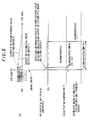
- Fig. 1 is a structure diagram of the first embodiment of an optical receiving unit including a signal break detecting circuit according to the present invention.
- the optical receiving unit comprises a coupling capacitor 1 for removing DC component of data signal which is transformed from optical signal to electric signal, a limiter amplifier (LIM) 2 for inputting data signal through the coupling capacitor 1, a DC feedback circuit (DCFB) 3 for providing offset voltage to data signal inputted to the limiter amplifier 2 and a signal break detecting circuit.
- LIM limiter amplifier
- DCFB DC feedback circuit
- the signal break detecting circuit comprises a first full-wave rectifying circuit 4 for full-wave rectifying output of the limiter amplifier 2, a peak value detecting circuit (peak DET) 5 for detecting a peak value in the first full-wave rectifying circuit 4, an average value detecting circuit (Ave DET) 6 for detecting an average value of output of the limiter amplifier 2, a second full-wave rectifying circuit 7 for full-wave rectifying output of the average value detecting circuit 6, a differential amplifier (Diff Amp) 8 for amplifying a difference between output of the peak value detecting circuit 5 and output of the second full-wave rectifying circuit 7 and a comparator (Comp) 9 for dispatching alarm output if output of the differential amplifier 8 drops below a reference voltage Vth.
- the limiter amplifier 2 may be of other means like AGC amplifier as long as it amplifies data signal which is transformed from optical signal to electric signal to a predetermined amplitude. Further, the comparator 9 may be provided with hysteresis characteristic to suppress deflection in the vicinity of the reference voltage Vth.
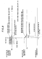
- Figs. 2, 3 are timing charts indicating an operation of the first embodiment.
- data signal which is output of the limiter amplifier 2
- the output of the average value detecting circuit 6 is of the same voltage as VDC.
- the voltage approaches the low level VL gradually following a time constant of the average value detecting circuit 6 and after that, converges to a level VDC according to any smaller time constant of a time constant of the DC feedback circuit 3 and a time constant of AC coupling with the coupling capacitor 1 (see Ave DET output 51 of the same Figure(A)).
- the time constant of the average value detecting circuit 6 needs to be slower than the specified same sign continuity and further faster than any smaller time constant of the time constant of the DC feedback circuit 3 and the time constant of AC coupling with the coupling capacitor 1.
- the voltage approaches the high level VH gradually according to the time constant of the average value detecting circuit 6. After that, the voltage converges to the level VDC according to any small time constant of the time constant of the DC feedback circuit 3 and the time constant of AC coupling with the coupling capacitor 1 (see output 52 of the same Figure(A)).
- the signal By passing the output of the average value detecting circuit 6 through the second full-wave rectifying circuit 7, the signal can be outputted to the same positive level side as the output of the peak value detecting circuit 5 as shown in Fig. 3(A), regardless of which a level just before a break of the data signal is of positive level or negative level.
- the output of the peak value detecting circuit 5 converges to level VDC according to any smaller time constant of the time constant of the DC feedback circuit 3 and the time constant of AC coupling with the coupling capacitor 1 regardless of which a level just before the break of the data signal is of positive level or negative level.
- the discharge time constant of the peak value detecting circuit 5 needs to be faster than any smaller time constant of the time constant of the DC feedback circuit 3 and the time constant of AC coupling with the coupling capacitor 1.
- the peak value detecting circuit 5 detects an envelope of the first full-wave rectifying circuit 4 and when the data signal breaks, the voltage converges to level VDC according to any smaller time constant of the time constant of the DC feedback circuit 3 and the time constant of AC coupling with the coupling capacitor 1.
- the difference between the output of the peak value detecting circuit 5 and the output of the second full-wave rectifying circuit 7 is amplified with the differential amplifier 8 and if this difference drops below the reference voltage vth, the comparator dispatches an alarm (see Figs. 3 (B), (C) ) .
- a differential curve between the output of the peak value detecting circuit 5 and the output of the second full-wave rectifying circuit 7 shown in Fig 3(B) is inverted from positive level to negative level.
- a difference between the output of the peak value detecting circuit 5 and the output of the second full-wave rectifying circuit 7 is amplified with the differential amplifier 8 and if this difference increases over the reference voltage Vth, the comparator 9 dispatches an alarm.
- Fig. 3(D) shows a timing chart of conventional art in which data signal break is detected by detecting that a peak value of reception signal drops to a predetermined value. If comparing Fig. 3 (C ) with Fig. 3(D), it is apparent that according to the present invention (see Fig. 3 (C ) ) , time required for detecting data signal can be reduced with respect to the conventional case.
- Fig. 4 shows a structure diagram of the second embodiment and Fig. 5 is a timing chart indicating an operation of the second embodiment. Meanwhile, in Fig. 4, like reference numerals are attached to the same components as Fig. 1 and a description thereof is omitted.
- the feature of the signal break detecting circuit of the second embodiment is that a second average value detecting circuit (Ave DET2) 11 is employed instead of the peak value detecting circuit 5 of the first embodiment,
- a detecting circuit which does not need so high speed operation as the peak value detecting circuit can be achieved with the average value detecting circuit 11 (see Figs. 5(B), (C)).
- Fig. 5(D) shows a timing chart of the conventional art in which the data signal break is detected by detecting that the peak value of reception signal drops to a predetermined value.
- Fig. 6 shows a structure diagram of the third embodiment and Figs. 7, 8 are timing charts showing an operation of the third embodiment. Meanwhile, in Fig. 6, like reference numerals are attached to the same components as Fig. 1 and a description thereof is omitted.
- the feature of the third embodiment is that the signal break detecting circuit of the third embodiment is so constructed that after the data signal is half-wave rectified with the first half-wave rectifying circuit 10, it is inputted to the peak value detecting circuit 5 and the average value detecting circuit 6 and that the single half-wave rectifying circuit 10 can do the same work which the two full-wave rectifying circuits 4, 7 do.
- the output of the average value detecting circuit 6 when there is data signal becomes an intermediate voltage between the level VDC and the high level VH. Then, when the level just before the data signal breaks is of high level VH, the voltage approaches the high level VH gradually according to the time constant of the average value detecting circuit 6 like the first embodiment. After that, it converges to the level VDC according to any smaller time constant of the time constant of the DC feedback circuit 3 and the time constant of AC coupling with the coupling capacitor 1 (see output 71 of Fig. 7(A)).
- Fig. 7(B) shows the relation between the difference in the output between the peak value detecting circuit 5 and the average value detecting circuit 6 and the reference voltage Vth.
- Fig. 7(C) shows an alarm dispatch timing.
- the output of the average value detecting circuit 6 converges to the level VDC according to the time constant of the average value detecting circuit 6 (see output 72 of Fig. 8(A)).
- the output of the peak value detecting circuit 5 converges to the level VDC according to discharge time constant of the peak value detecting circuit 5 (see output 73 of Fig. 8(A)).
- output 72 of the average value detecting circuit 6 and output 73 of the peak value detecting circuit 5 in Fig. 8(A) converge to the level VDC in a shorter time as compared to the output waveform of Fig. 7(A).
- Fig. 8(B) shows the relation between the difference in output between the peak value detecting circuit 5 and the average value detecting circuit 6 and the reference voltage Vth and Fig. 8(C) shows an alarm dispatch timing.
- the present invention achieves a signal break detecting circuit for detecting a signal break in reception signal, comprising: a first value detecting means for detecting a first value obtained corresponding to the amplitude of the reception signal; a second value detecting means for detecting a second value which is obtained corresponding to the amplitude of the reception signal and different from the first value; a difference detecting means for detecting a difference between the first value and the second value; and a comparing means which compares output of the difference detecting means with a predetermined reference value and outputs a comparison result. Consequently, time necessary for detecting data signal break can be reduced.
- alarm dispatch time response speed
- the alarm dispatch time can be controlled according to the time constant of the average value detecting circuit without depending on any smaller time constant of the time constant of the DC feedback circuit 3 and the time constant of AC coupling of the coupling capacitor 1. Consequently, the alarm dispatch time can be quickened as compared to when alarm is dispatched with only output of the peak value detecting circuit 5.
- the second effect is that by monitoring a difference between the average value of data signal and full-wave rectified peak value, signal level can be detected in a short time regardless of offset of the data signal.
- the present invention is effective if there is offset in a limiter amplifier or the like and further, also effective in a case of optimizing the threshold by providing the limiter amplifier with offset intentionally for adaptive threshold control (ATC).
- ATC adaptive threshold control
- the third effect is that due to the full-wave rectification, the alarm can be dispatched regardless of a level just before data signal breaks.
- the fourth effect is that power consumption can be reduced because such a high speed circuit as a flip-flop circuit and logic IC is not employed.
Landscapes
- Physics & Mathematics (AREA)
- Electromagnetism (AREA)
- Engineering & Computer Science (AREA)
- Computer Networks & Wireless Communication (AREA)
- Signal Processing (AREA)
- Monitoring And Testing Of Transmission In General (AREA)
- Dc Digital Transmission (AREA)
- Manipulation Of Pulses (AREA)
- Optical Communication System (AREA)
Applications Claiming Priority (2)
| Application Number | Priority Date | Filing Date | Title |
|---|---|---|---|
| JP2000293232 | 2000-09-27 | ||
| JP2000293232A JP3719119B2 (ja) | 2000-09-27 | 2000-09-27 | 光受信装置 |
Publications (3)
| Publication Number | Publication Date |
|---|---|
| EP1193902A2 true EP1193902A2 (de) | 2002-04-03 |
| EP1193902A3 EP1193902A3 (de) | 2004-10-20 |
| EP1193902B1 EP1193902B1 (de) | 2005-12-28 |
Family
ID=18776055
Family Applications (1)
| Application Number | Title | Priority Date | Filing Date |
|---|---|---|---|
| EP01122642A Expired - Lifetime EP1193902B1 (de) | 2000-09-27 | 2001-09-27 | Schaltkreis zur Erfassung einer Signalunterbrechung |
Country Status (5)
| Country | Link |
|---|---|
| US (1) | US6636348B2 (de) |
| EP (1) | EP1193902B1 (de) |
| JP (1) | JP3719119B2 (de) |
| CA (1) | CA2357813C (de) |
| DE (1) | DE60116213T2 (de) |
Cited By (3)
| Publication number | Priority date | Publication date | Assignee | Title |
|---|---|---|---|---|
| US6636348B2 (en) * | 2000-09-27 | 2003-10-21 | Nec Corporation | Signal break detecting circuit |
| EP1376901A3 (de) * | 2002-06-27 | 2004-03-31 | Matsushita Electric Industrial Co., Ltd. | Stationsnahe Einrichtung, teilnehmernahe Einrichtung und optisches Übertragungssystem |
| US10444261B2 (en) | 2014-12-22 | 2019-10-15 | Sony Corporation | Signal detector, electronic device, and method for controlling signal detector |
Families Citing this family (9)
| Publication number | Priority date | Publication date | Assignee | Title |
|---|---|---|---|---|
| US7146433B2 (en) * | 2002-02-01 | 2006-12-05 | Lenovo Singapore Pte. Ltd | Extending an allowable transmission distance between a wireless device and an access point by communication with intermediate wireless devices |
| US7751725B2 (en) * | 2005-08-10 | 2010-07-06 | Sumitomo Electric Industries, Ltd. | Optical receiver with monitoring unit and a method for detecting consecutive identical state of optical signal |
| JP4760312B2 (ja) * | 2005-11-07 | 2011-08-31 | 住友電気工業株式会社 | 光受信器 |
| JP4940988B2 (ja) * | 2007-02-19 | 2012-05-30 | 富士通オプティカルコンポーネンツ株式会社 | 光受信装置 |
| JP2010093353A (ja) * | 2008-10-03 | 2010-04-22 | Sumitomo Electric Ind Ltd | 光受信器 |
| US7821300B2 (en) * | 2008-12-03 | 2010-10-26 | International Business Machines Corporation | System and method for converting between CML signal logic families |
| JP5261318B2 (ja) * | 2009-08-13 | 2013-08-14 | Necエンジニアリング株式会社 | データ信号断検出回路 |
| JP5456094B2 (ja) * | 2012-04-27 | 2014-03-26 | 日本電信電話株式会社 | 受信光信号のクロスポイント検出回路およびそれを用いた光受信装置 |
| CN110736890B (zh) * | 2019-10-31 | 2021-07-20 | 国网河南省电力公司信息通信公司 | 一种配电网数据安全预警系统 |
Family Cites Families (18)
| Publication number | Priority date | Publication date | Assignee | Title |
|---|---|---|---|---|
| FR2475826A1 (fr) * | 1980-02-12 | 1981-08-14 | Lignes Telegraph Telephon | Dispositif de declenchement d'alarme pour une insuffisance du niveau de transmission, pour module recepteur d'un systeme de transmission sur fibre optique |
| JPS61128637A (ja) * | 1984-11-28 | 1986-06-16 | Hitachi Ltd | 光入力信号断検出回路 |
| JPS62284519A (ja) * | 1986-06-02 | 1987-12-10 | Toshiba Corp | 信号検出回路 |
| JPH0345069A (ja) | 1989-07-13 | 1991-02-26 | Toshiba Corp | ファクシミリ装置 |
| JPH0379141A (ja) | 1989-08-23 | 1991-04-04 | Fujitsu Ltd | 光信号入力断検出回路 |
| JPH05114842A (ja) * | 1991-10-21 | 1993-05-07 | Hitachi Ltd | 入力信号断検出回路 |
| JPH05260032A (ja) | 1992-02-04 | 1993-10-08 | Nec Corp | タイミング信号断検出回路 |
| JPH07245540A (ja) * | 1994-01-12 | 1995-09-19 | Fujitsu Ltd | 光ディジタル通信用の光受信装置 |
| EP0667533A3 (de) * | 1994-02-14 | 1996-06-12 | Hewlett Packard Co | Signalverlustdetektor. |
| IT1268058B1 (it) * | 1994-05-20 | 1997-02-20 | Cselt Centro Studi Lab Telec O | Procedimento e dispositivo per il controllo della potenza di picco di un trasmettitore laser in sistemi di trasmissione ottica discontinua. |
| US5543783A (en) * | 1994-05-20 | 1996-08-06 | Caddx-Caddi Controls, Inc. | Glass break detector and a method therefor |
| JP3363003B2 (ja) * | 1995-10-03 | 2003-01-07 | 株式会社日立製作所 | 光増幅装置及び光増幅装置を用いた光伝送システム |
| CA2172873C (en) * | 1996-03-28 | 2002-03-12 | Kim Byron Roberts | Method of determining optical amplifier failures |
| JP3045069B2 (ja) | 1996-04-12 | 2000-05-22 | 日本電気株式会社 | 光入力断検出方法と光入力断検出回路 |
| JP3107033B2 (ja) * | 1998-03-09 | 2000-11-06 | 日本電気株式会社 | 光増幅装置とこれを含む光伝送装置の伝送路破断点検出方法および光増幅装置を用いた双方向波長多重光伝送装置 |
| US6222668B1 (en) * | 1998-05-08 | 2001-04-24 | Nortel Networks Limited | Fast loss of signal (LOS) detection for bidirectional optical amplifiers |
| US6259517B1 (en) * | 1998-11-17 | 2001-07-10 | Kaiser Optical Systems, Inc. | Optical fiber breakage detection system |
| JP3719119B2 (ja) * | 2000-09-27 | 2005-11-24 | 日本電気株式会社 | 光受信装置 |
-
2000
- 2000-09-27 JP JP2000293232A patent/JP3719119B2/ja not_active Expired - Fee Related
-
2001
- 2001-09-26 US US09/962,113 patent/US6636348B2/en not_active Expired - Fee Related
- 2001-09-26 CA CA002357813A patent/CA2357813C/en not_active Expired - Lifetime
- 2001-09-27 EP EP01122642A patent/EP1193902B1/de not_active Expired - Lifetime
- 2001-09-27 DE DE60116213T patent/DE60116213T2/de not_active Expired - Lifetime
Cited By (3)
| Publication number | Priority date | Publication date | Assignee | Title |
|---|---|---|---|---|
| US6636348B2 (en) * | 2000-09-27 | 2003-10-21 | Nec Corporation | Signal break detecting circuit |
| EP1376901A3 (de) * | 2002-06-27 | 2004-03-31 | Matsushita Electric Industrial Co., Ltd. | Stationsnahe Einrichtung, teilnehmernahe Einrichtung und optisches Übertragungssystem |
| US10444261B2 (en) | 2014-12-22 | 2019-10-15 | Sony Corporation | Signal detector, electronic device, and method for controlling signal detector |
Also Published As
| Publication number | Publication date |
|---|---|
| EP1193902A3 (de) | 2004-10-20 |
| DE60116213D1 (de) | 2006-02-02 |
| US6636348B2 (en) | 2003-10-21 |
| CA2357813A1 (en) | 2002-03-27 |
| CA2357813C (en) | 2004-08-03 |
| JP2002111587A (ja) | 2002-04-12 |
| JP3719119B2 (ja) | 2005-11-24 |
| DE60116213T2 (de) | 2006-06-22 |
| US20020036810A1 (en) | 2002-03-28 |
| EP1193902B1 (de) | 2005-12-28 |
Similar Documents
| Publication | Publication Date | Title |
|---|---|---|
| CA2357813C (en) | Signal break detecting circuit | |
| US5483574A (en) | Communication terminal equipment | |
| US5994999A (en) | Low voltage link for transmitting on/off orders | |
| EP1355436B1 (de) | Optischer Empfänger im Burstmodus zur Erzeugung eines Rücksetzsignals für eine automatische Schwellwertanpassungsschaltung zwischen aufeinanderfolgenden Bursts | |
| US6034995A (en) | System for the transmission of data via a differential bus | |
| EP1355437B1 (de) | Niedrigstwertdetektor für einen optischen Empfänger im Burstbetrieb | |
| US5526528A (en) | Abnormal transmission stopping circuit for transmitter | |
| US5379143A (en) | Optical regenerative-repeater system | |
| JPH0946417A (ja) | リングトリップ回路 | |
| EP0410445B1 (de) | Optischer Empfänger mit Mitteln zum Verhindern von Störungen aufgrund von Geräuschanwesenheit | |
| US6734918B2 (en) | Data slicer circuit | |
| US7257323B2 (en) | Signal-off detection circuit and optical receiving device using the same | |
| US5805319A (en) | Circuit for discriminating the presence of extraordinariness in an output signal | |
| US20020089233A1 (en) | Power supply device and electronic equipment | |
| JPH10164223A (ja) | リングトリップ回路 | |
| EP0874481A2 (de) | Optisches Teilnehmer-Anschlussnetzsystem | |
| US4754472A (en) | Telecommunication systems | |
| JP2616480B2 (ja) | バースト光受信回路 | |
| US4167682A (en) | Overshoot suppression circuitry for ternary pulses | |
| JPS5826249B2 (ja) | ホゴケイデンソウチ | |
| JP3673751B2 (ja) | 信号断検出回路及びそれを用いた光受信装置 | |
| US7136597B2 (en) | Decision system for modulated electrical signals | |
| JPH11122208A (ja) | Ais信号挿入装置 | |
| JP2513133B2 (ja) | 電気/光変換装置 | |
| KR0165619B1 (ko) | 무선통신시스템용 전원장치 |
Legal Events
| Date | Code | Title | Description |
|---|---|---|---|
| PUAI | Public reference made under article 153(3) epc to a published international application that has entered the european phase |
Free format text: ORIGINAL CODE: 0009012 |
|
| AK | Designated contracting states |
Kind code of ref document: A2 Designated state(s): AT BE CH CY DE DK ES FI FR GB GR IE IT LI LU MC NL PT SE TR |
|
| AX | Request for extension of the european patent |
Free format text: AL;LT;LV;MK;RO;SI |
|
| PUAL | Search report despatched |
Free format text: ORIGINAL CODE: 0009013 |
|
| AK | Designated contracting states |
Kind code of ref document: A3 Designated state(s): AT BE CH CY DE DK ES FI FR GB GR IE IT LI LU MC NL PT SE TR |
|
| AX | Request for extension of the european patent |
Extension state: AL LT LV MK RO SI |
|
| RIC1 | Information provided on ipc code assigned before grant |
Ipc: 7H 04B 10/158 A Ipc: 7H 04B 10/08 B |
|
| 17P | Request for examination filed |
Effective date: 20040914 |
|
| 17Q | First examination report despatched |
Effective date: 20041126 |
|
| GRAP | Despatch of communication of intention to grant a patent |
Free format text: ORIGINAL CODE: EPIDOSNIGR1 |
|
| AKX | Designation fees paid |
Designated state(s): DE FR GB IT |
|
| GRAS | Grant fee paid |
Free format text: ORIGINAL CODE: EPIDOSNIGR3 |
|
| GRAA | (expected) grant |
Free format text: ORIGINAL CODE: 0009210 |
|
| AK | Designated contracting states |
Kind code of ref document: B1 Designated state(s): DE FR GB IT |
|
| REG | Reference to a national code |
Ref country code: GB Ref legal event code: FG4D |
|
| REF | Corresponds to: |
Ref document number: 60116213 Country of ref document: DE Date of ref document: 20060202 Kind code of ref document: P |
|
| ET | Fr: translation filed | ||
| PLBE | No opposition filed within time limit |
Free format text: ORIGINAL CODE: 0009261 |
|
| STAA | Information on the status of an ep patent application or granted ep patent |
Free format text: STATUS: NO OPPOSITION FILED WITHIN TIME LIMIT |
|
| 26N | No opposition filed |
Effective date: 20060929 |
|
| PGFP | Annual fee paid to national office [announced via postgrant information from national office to epo] |
Ref country code: GB Payment date: 20120926 Year of fee payment: 12 |
|
| PGFP | Annual fee paid to national office [announced via postgrant information from national office to epo] |
Ref country code: FR Payment date: 20120926 Year of fee payment: 12 Ref country code: DE Payment date: 20120919 Year of fee payment: 12 Ref country code: IT Payment date: 20120922 Year of fee payment: 12 |
|
| REG | Reference to a national code |
Ref country code: DE Ref legal event code: R119 Ref document number: 60116213 Country of ref document: DE |
|
| GBPC | Gb: european patent ceased through non-payment of renewal fee |
Effective date: 20130927 |
|
| REG | Reference to a national code |
Ref country code: DE Ref legal event code: R079 Ref document number: 60116213 Country of ref document: DE Free format text: PREVIOUS MAIN CLASS: H04B0010158000 Ipc: H04B0010660000 |
|
| REG | Reference to a national code |
Ref country code: FR Ref legal event code: ST Effective date: 20140530 |
|
| REG | Reference to a national code |
Ref country code: DE Ref legal event code: R079 Ref document number: 60116213 Country of ref document: DE Free format text: PREVIOUS MAIN CLASS: H04B0010158000 Ipc: H04B0010660000 Effective date: 20140610 Ref country code: DE Ref legal event code: R119 Ref document number: 60116213 Country of ref document: DE Effective date: 20140401 |
|
| PG25 | Lapsed in a contracting state [announced via postgrant information from national office to epo] |
Ref country code: GB Free format text: LAPSE BECAUSE OF NON-PAYMENT OF DUE FEES Effective date: 20130927 |
|
| PG25 | Lapsed in a contracting state [announced via postgrant information from national office to epo] |
Ref country code: DE Free format text: LAPSE BECAUSE OF NON-PAYMENT OF DUE FEES Effective date: 20140401 Ref country code: FR Free format text: LAPSE BECAUSE OF NON-PAYMENT OF DUE FEES Effective date: 20130930 Ref country code: IT Free format text: LAPSE BECAUSE OF NON-PAYMENT OF DUE FEES Effective date: 20130927 |