EP1190480B1 - Dynamically-switched power converter - Google Patents
Dynamically-switched power converter Download PDFInfo
- Publication number
- EP1190480B1 EP1190480B1 EP00944805A EP00944805A EP1190480B1 EP 1190480 B1 EP1190480 B1 EP 1190480B1 EP 00944805 A EP00944805 A EP 00944805A EP 00944805 A EP00944805 A EP 00944805A EP 1190480 B1 EP1190480 B1 EP 1190480B1
- Authority
- EP
- European Patent Office
- Prior art keywords
- capacitor
- switching matrix
- voltage
- fly
- power management
- Prior art date
- Legal status (The legal status is an assumption and is not a legal conclusion. Google has not performed a legal analysis and makes no representation as to the accuracy of the status listed.)
- Expired - Lifetime
Links
Images


Classifications
-
- H—ELECTRICITY
- H02—GENERATION; CONVERSION OR DISTRIBUTION OF ELECTRIC POWER
- H02J—CIRCUIT ARRANGEMENTS OR SYSTEMS FOR SUPPLYING OR DISTRIBUTING ELECTRIC POWER; SYSTEMS FOR STORING ELECTRIC ENERGY
- H02J7/00—Circuit arrangements for charging or depolarising batteries or for supplying loads from batteries
-
- H—ELECTRICITY
- H01—ELECTRIC ELEMENTS
- H01M—PROCESSES OR MEANS, e.g. BATTERIES, FOR THE DIRECT CONVERSION OF CHEMICAL ENERGY INTO ELECTRICAL ENERGY
- H01M6/00—Primary cells; Manufacture thereof
- H01M6/50—Methods or arrangements for servicing or maintenance, e.g. for maintaining operating temperature
- H01M6/5044—Cells or batteries structurally combined with cell condition indicating means
-
- H—ELECTRICITY
- H01—ELECTRIC ELEMENTS
- H01M—PROCESSES OR MEANS, e.g. BATTERIES, FOR THE DIRECT CONVERSION OF CHEMICAL ENERGY INTO ELECTRICAL ENERGY
- H01M10/00—Secondary cells; Manufacture thereof
- H01M10/42—Methods or arrangements for servicing or maintenance of secondary cells or secondary half-cells
- H01M10/48—Accumulators combined with arrangements for measuring, testing or indicating the condition of cells, e.g. the level or density of the electrolyte
- H01M10/488—Cells or batteries combined with indicating means for external visualization of the condition, e.g. by change of colour or of light density
-
- H—ELECTRICITY
- H02—GENERATION; CONVERSION OR DISTRIBUTION OF ELECTRIC POWER
- H02M—APPARATUS FOR CONVERSION BETWEEN AC AND AC, BETWEEN AC AND DC, OR BETWEEN DC AND DC, AND FOR USE WITH MAINS OR SIMILAR POWER SUPPLY SYSTEMS; CONVERSION OF DC OR AC INPUT POWER INTO SURGE OUTPUT POWER; CONTROL OR REGULATION THEREOF
- H02M3/00—Conversion of dc power input into dc power output
- H02M3/02—Conversion of dc power input into dc power output without intermediate conversion into ac
- H02M3/04—Conversion of dc power input into dc power output without intermediate conversion into ac by static converters
- H02M3/06—Conversion of dc power input into dc power output without intermediate conversion into ac by static converters using resistors or capacitors, e.g. potential divider
- H02M3/07—Conversion of dc power input into dc power output without intermediate conversion into ac by static converters using resistors or capacitors, e.g. potential divider using capacitors charged and discharged alternately by semiconductor devices with control electrode, e.g. charge pumps
-
- H—ELECTRICITY
- H02—GENERATION; CONVERSION OR DISTRIBUTION OF ELECTRIC POWER
- H02M—APPARATUS FOR CONVERSION BETWEEN AC AND AC, BETWEEN AC AND DC, OR BETWEEN DC AND DC, AND FOR USE WITH MAINS OR SIMILAR POWER SUPPLY SYSTEMS; CONVERSION OF DC OR AC INPUT POWER INTO SURGE OUTPUT POWER; CONTROL OR REGULATION THEREOF
- H02M3/00—Conversion of dc power input into dc power output
- H02M3/02—Conversion of dc power input into dc power output without intermediate conversion into ac
- H02M3/04—Conversion of dc power input into dc power output without intermediate conversion into ac by static converters
- H02M3/10—Conversion of dc power input into dc power output without intermediate conversion into ac by static converters using discharge tubes with control electrode or semiconductor devices with control electrode
- H02M3/145—Conversion of dc power input into dc power output without intermediate conversion into ac by static converters using discharge tubes with control electrode or semiconductor devices with control electrode using devices of a triode or transistor type requiring continuous application of a control signal
- H02M3/155—Conversion of dc power input into dc power output without intermediate conversion into ac by static converters using discharge tubes with control electrode or semiconductor devices with control electrode using devices of a triode or transistor type requiring continuous application of a control signal using semiconductor devices only
- H02M3/156—Conversion of dc power input into dc power output without intermediate conversion into ac by static converters using discharge tubes with control electrode or semiconductor devices with control electrode using devices of a triode or transistor type requiring continuous application of a control signal using semiconductor devices only with automatic control of output voltage or current, e.g. switching regulators
- H02M3/158—Conversion of dc power input into dc power output without intermediate conversion into ac by static converters using discharge tubes with control electrode or semiconductor devices with control electrode using devices of a triode or transistor type requiring continuous application of a control signal using semiconductor devices only with automatic control of output voltage or current, e.g. switching regulators including plural semiconductor devices as final control devices for a single load
- H02M3/1588—Conversion of dc power input into dc power output without intermediate conversion into ac by static converters using discharge tubes with control electrode or semiconductor devices with control electrode using devices of a triode or transistor type requiring continuous application of a control signal using semiconductor devices only with automatic control of output voltage or current, e.g. switching regulators including plural semiconductor devices as final control devices for a single load comprising at least one synchronous rectifier element
-
- H—ELECTRICITY
- H02—GENERATION; CONVERSION OR DISTRIBUTION OF ELECTRIC POWER
- H02J—CIRCUIT ARRANGEMENTS OR SYSTEMS FOR SUPPLYING OR DISTRIBUTING ELECTRIC POWER; SYSTEMS FOR STORING ELECTRIC ENERGY
- H02J2207/00—Indexing scheme relating to details of circuit arrangements for charging or depolarising batteries or for supplying loads from batteries
- H02J2207/20—Charging or discharging characterised by the power electronics converter
-
- Y—GENERAL TAGGING OF NEW TECHNOLOGICAL DEVELOPMENTS; GENERAL TAGGING OF CROSS-SECTIONAL TECHNOLOGIES SPANNING OVER SEVERAL SECTIONS OF THE IPC; TECHNICAL SUBJECTS COVERED BY FORMER USPC CROSS-REFERENCE ART COLLECTIONS [XRACs] AND DIGESTS
- Y02—TECHNOLOGIES OR APPLICATIONS FOR MITIGATION OR ADAPTATION AGAINST CLIMATE CHANGE
- Y02B—CLIMATE CHANGE MITIGATION TECHNOLOGIES RELATED TO BUILDINGS, e.g. HOUSING, HOUSE APPLIANCES OR RELATED END-USER APPLICATIONS
- Y02B40/00—Technologies aiming at improving the efficiency of home appliances, e.g. induction cooking or efficient technologies for refrigerators, freezers or dish washers
-
- Y—GENERAL TAGGING OF NEW TECHNOLOGICAL DEVELOPMENTS; GENERAL TAGGING OF CROSS-SECTIONAL TECHNOLOGIES SPANNING OVER SEVERAL SECTIONS OF THE IPC; TECHNICAL SUBJECTS COVERED BY FORMER USPC CROSS-REFERENCE ART COLLECTIONS [XRACs] AND DIGESTS
- Y02—TECHNOLOGIES OR APPLICATIONS FOR MITIGATION OR ADAPTATION AGAINST CLIMATE CHANGE
- Y02B—CLIMATE CHANGE MITIGATION TECHNOLOGIES RELATED TO BUILDINGS, e.g. HOUSING, HOUSE APPLIANCES OR RELATED END-USER APPLICATIONS
- Y02B70/00—Technologies for an efficient end-user side electric power management and consumption
- Y02B70/10—Technologies improving the efficiency by using switched-mode power supplies [SMPS], i.e. efficient power electronics conversion e.g. power factor correction or reduction of losses in power supplies or efficient standby modes
-
- Y—GENERAL TAGGING OF NEW TECHNOLOGICAL DEVELOPMENTS; GENERAL TAGGING OF CROSS-SECTIONAL TECHNOLOGIES SPANNING OVER SEVERAL SECTIONS OF THE IPC; TECHNICAL SUBJECTS COVERED BY FORMER USPC CROSS-REFERENCE ART COLLECTIONS [XRACs] AND DIGESTS
- Y02—TECHNOLOGIES OR APPLICATIONS FOR MITIGATION OR ADAPTATION AGAINST CLIMATE CHANGE
- Y02E—REDUCTION OF GREENHOUSE GAS [GHG] EMISSIONS, RELATED TO ENERGY GENERATION, TRANSMISSION OR DISTRIBUTION
- Y02E60/00—Enabling technologies; Technologies with a potential or indirect contribution to GHG emissions mitigation
- Y02E60/10—Energy storage using batteries
Definitions
- the present invention relates to DC/DC power supply controllers, and more particularly to regulated capacitive-only or capacitive/inductive power converters for integrated power management systems.
- the electronics in a portable electronic device generally require direct current (DC) electrical power.
- DC direct current
- one or more batteries are used as an energy source to provide this DC electrical power.
- the energy source such as consumer batteries of standard sizes such as AAA, AA, A, C, D and prismatic 9V, would be perfectly matched to the energy requirements of the portable electronic device. Improvements in electrochemical formulations, such as alkaline and lithium electrochemical cells, have satisfied to a limited degree needs for batteries having increased shelf life, increased stored charge, and peak capacity. With even these changes, a number of deficiencies exist.
- the voltage and current from the batteries are unsuitable for directly powering the electronics of the portable electronic device.
- the voltage level determined from the batteries may differ from the voltage level required by the device electronically.
- some portions of the electronics may operate at a different voltage level than other portions, thereby requiring different energy source voltage levels.
- batteries are often unable to respond quickly to rapid fluctuations in current demand by a device.
- the power converter 20 may "step up” (i.e., boost) or “step down” the voltage. That is, the converter 20 may increase or decrease an input voltage Vs from the energy source 12 across a pair of input terminals 24, 25 to an output voltage V O provided to the load device 14 across a pair of output terminals 26, 27.
- the power converter 20 may also store an amount of energy to satisfy a brief spike or increase in demand by the load device 14 that the energy source 12 is unable to provide.
- the power converter 20 may also regulate the output voltage V O , keeping it close to the desired output voltage level and reducing rapid fluctuations that may cause detrimental noise or cause undesirable performance of the load device 14. Such fluctuations may occur due to changes in demand by the load, induced noise from external electromagnetic sources, characteristics of the energy source 12, and/or noise from other components in the power supply 16.
- switching power converters 20 are used in portable devices due to their suitable size and cost.
- capacitive-only charge pump or inductive/capacitive switching power converters 20 typically rely upon oscillatory switching between a charge and discharge state to transfer power from an energy source such as an electrochemical voltaic cell 12 to a load device 14. Each switching of state incurs a significant consumption of power that reduces the shelf-life of the voltaic cell.
- the power converters typically cannot be optimized for a wide array of available types of electrochemical voltaic cells 12 (e. g., lithium, alkaline). Consequently, such power converters 20 generally only regulated voltage at a consider loss of efficiency or boost the voltage derived from the cell 12 in an unregulated fashion.
- electrochemical voltaic cells 12 e. g., lithium, alkaline
- German Utility Model DE 29605699 discloses a battery provided with a normal output voltage in the region of 3.6V to 5 V, and a radio device with a capacitor parallel switched to the transmitter for buffering.
- the positive battery output voltage is transformed up to, for example, 30 V to charge the capacitor.
- the battery current is only slightly pulsed.
- the capacitor is charged and discharged during the transmission process using an inductor.
- the capacitor voltage sinks to, for example, 10 V so the capacitor voltage is first raised with respect to the battery output voltage and then dropped to the required supply voltage of the transmitter stage.
- European patent application EP 653798 discloses a battery and a voltage converter in order to maintain a constant output voltage when the battery voltage drops. In order to make it as easy as possible to handle the battery and the voltage converter, the battery and the voltage converter are combined in one mechanical unit.
- the invention overcomes the above-noted and other deficiencies of the prior art by providing a power management circuit configured to adjust an output voltage across positive and negative terminals of a battery, the battery further including a voltaic cell having a positive electrode and a negative electrode, a fly capacitor, and a load capacitor electrically coupled across the terminals, the power management circuit comprising: a switching matrix being electrically switchable between a charge mode and a discharge mode, wherein the switching matrix in charge mode comprises being configured to charge the fly capacitor by electrically coupling the fly capacitor in series combination with the voltaic cell, and wherein the switching matrix in discharge mode comprises being configured to discharge the fly capacitor into the load capacitor by electrically coupling the fly capacitor in series combination with the load capacitor; and a switching matrix controller operatively coupled to the switching matrix to select the charge and discharge mode only as needed to keep the output voltage at a desired value.
- the power converter utilizes a load capacitor that receives a transfer of charge from a fly capacitor. More particularly, the fly capacitor is switched dynamically to accommodate varying loads on the load capacitor to efficiently transfer charge.
- the power converter comprises a charge pump including a switching matrix controlling a fly capacitor wherein the fly capacitor is switched to charge mode electrically parallel to a voltaic cell of the battery. Thereafter, the switching matrix switches to a discharge mode where the potential of the fly capacitor is additively placed in series with the voltaic cell, and the combination is electrically coupled across the load capacitor to discharge the stored charge in the fly capacitor into the load capacitor.
- the switching of the fly capacitor is dynamically performed by a switching matrix controller, rather than merely oscillating the state of the switching matrix without regard to electrical load. Dynamic control allows for power conservation during periods of low power demand on the battery.
- Another aspect is to dynamically control the switching matrix by incorporating a comparator into the switching matrix controller.
- a comparator also provided is a voltage reference and temperature compensation for the voltage reference for the comparator to use in comparing the output voltage to a predetermined threshold.
- an internal power supply is provided to bias the power converter, especially for voltaic cells having a relatively low nominal voltage.
- the power converter is largely fabricated as an Application Specific Integrated Circuit (ASIC).
- ASIC Application Specific Integrated Circuit
- FET Field Effect Transistors
- a power converter as required by the load on a battery provides additional peak capacity and/or increased power efficiency, among other advantages.
- dynamic switching lends itself to a wide range of voltaic cells (e.g., electrochemical cells such as lithium, zinc acid, alkaline, etc.; electro mechanical cells, solar cells; etc.).
- dynamic control of a inductive-capacitive DC/DC power converter includes sensing an adequate state of charge of a load capacitor across the output terminals and stopping pulse width modulation control of the switching of an inductive element, a synchronous rectifier and a switch to reduce power consumption by the power converter.
- an electrical block diagram of a battery 28 includes a power converter 30 interposed between input terminals 32, 34 of a voltaic cell 36 and a positive output terminal 38 and negative output terminal 40 of the battery 28.
- the power converter 30 comprises a switched capacitive device 42 across a positive and negative output terminals 38, 40 whose mode is switched by a switching matrix 44.
- the switching matrix 44 is controlled by a signal S from a switching matrix controller 46 that generates the signal S in response to a measurement M received from the switching matrix 44.
- the ASIC 48 may further include a voltage reference 50, preferably extremely low power consuming with good stability, providing a reference voltage ( V REF ) signal to the switching matrix controller 46. Since some voltage references 50 may vary as a function of semiconductor temperature, temperature compensation 52 to the voltage reference 50 may also be included, such as a proportional-to-absolute-temperature circuit. Voltaic cells 14 such as lithium electrochemical cells have an inherent bandgap voltage reference that may utilized. As will be shown in more detail below, the ASIC 48 may further include an internal power supply 56 which allows efficient operation of other portions of the ASIC 48 at relatively low voltage levels of the source voltage V S .
- Fig. 4 is an electrical circuit for a noninverting switching matrix 44', fly capacitor C FLY , and output capacitor C OUT of Fig. 3, and depicts a simplified voltage doubler.
- switch signal S1 commands switch Q1 and switch Q3 closed
- switch signal S2 commands switch Q2 and switch Q4 closed
- capacitor C FLY charges to V S .
- switch signal S1 commands switch Q1 and switch Q3 open
- switch signal S2 commands switch Q2 and switch Q4 closed
- C FLY is level shifted upward by V S volts. This connects the fly capacitor C FLY to the output capacitor C OUT , allowing energy to be delivered to the output as necessary.
- the actual voltage is slightly lower than 2 x V S , since switches Q1-Q4 have resistance that drains charge from C OUT .
- the power efficiency of a switched capacitive device 42 is affected by three factors: the internal losses in the ASIC 48, the resistive losses of the capacitors C FLY , C OUT , and the conversion losses during charge transfer between the capacitors C FLY , C OUT .
- the charge pump output resistance R OUT is a function of the ESR of the fly capacitor C FLY and load capacitor C OUT and the internal switch resistance, as shown in the equation below. Minimizing the ESR of the load capacitor C OUT minimizes the total resistance R OUT . Using a larger flying capacitor C FLY reduces the output impedance and improves efficiency. Above a certain point, increasing the capacitance of the fly capacitor C FLY has a negligible effect because the output resistance R OUT becomes dominated by the resistance and capacitance of the internal switches. But when space is a constraint as in most batteries, it may be necessary to trade-off an achievable lower output resistance R OUT for the sake of small capacitor size.
- a capacitance value for the fly capacitor C FLY of about 10 uF or more is sufficient to supply the specified load current.
- Surface-mount ceramic capacitors within this capacitance range are suitable for a number of application for the fly capacitor C FLY , due to their small size, low cost, and low equivalent series resistance (ESR).
- ESR equivalent series resistance
- ceramic capacitors with X7R (or equivalent) low-temperature-coefficient dielectrics may be used advantageously.
- the output capacitor C OUT stores the charge transferred from the flying capacitor C FLY and services the load between charge/discharge cycles.
- a good general rule is to make the output capacitance C OUT at least ten times greater than that of the flying capacitance.
- High efficiency capacitors are those types of capacitors having relatively low charge leakage, for example double layer electrolytic capacitors (e.g., capacitors known as super capacitors, ultra capacitors, and power capacitors) and pseudo capacitors.
- double layer electrolytic capacitors e.g., capacitors known as super capacitors, ultra capacitors, and power capacitors
- pseudo capacitors e.g., pseudo capacitors.
- the ESR ripple contribution occurs as the output capacitor C OUT charges.
- the charging current creates a negative voltage pulse across the ESR of the output capacitor C OUT that recedes as the output capacitor C OUT charges.
- no charging current flows. This effect is even more pronounced in the case of a high efficiency capacitor.
- V RIPPLE(ESR) 2 x [(V S - 2 V O 2) / f OSC ] x [ 1 / (R OUT x (C FLY + C OUT ))], where R OUT is open-loop output impedance. If the ESR of the output capacitor C OUT is very small, as is likely when ceramic capacitors are used, V RIPPLE(TRANSFER) dominates. If the ESR is relatively large, as with low-cost tantalum capacitors, then V RIPPLE(ESR) dominates.
- Continuous mode is a constant frequency mode when the charge pump power converter 30 works continuously.
- the output voltage is quasi-linear so ripple is almost an irrelevant parameter.
- switches Q1 and Q2 may be advantageously preset to an "on" state to provide initial charge to the output capacitor C OUT to prevent parasitic latch-up of the ASIC 48, especially for electro voltaic cells having a nominal voltage of about 1.2 V to about 1.5 V.
- Fig. 4A is an electrical circuit of an inverting switching matrix 44", fly capacitor C FLY , and output capacitor C OUT of Fig. 4, illustrating the advantages of dynamic switching of a capacitive power converter 30 to achieve an inverted output.
- the negative voltage potential at the negative terminal 40 is lowered, by selectively switching switches SW0 and SW1.
- Fig. 5 is a three-dimensional plot of stored charge in the fly capacitor C FLY as a function of source voltage V S and the capacitance of the fly capacitor C FLY .
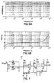
- FIGS. 6A and 6B are a representative complex impedance plot as a function of frequency for an ultra-capacitor, specifically an 8 F ultra-capacitor sold by Maxwell as a model Ultra PC223, illustrating its beneficial low impedance.
- Fig. 7 is an electrical circuit for an illustrative circuit for a first comparator 53 demonstrating an approach for the switching matrix controller 46 of Fig. 4.
- fly capacitor C FLY should advantageously be switched only when needed in a closed-loop approach, and not based on an open-loop oscillator approach.
- the basic idea is to switch the fly capacitor C FLY into the discharge mode when the output capacitor C OUT reaches a certain predetermined threshold voltage (V1). At this point, the fly capacitor C FLY will charge the output capacitor C OUT .
- V2 a certain voltage
- Fig. 8 is a voltage plot during the time interval required for the output capacitor C OUT to charge.
- Depicted is a voltage plot of a switch signal S1 to the switching matrix 44 switches Q1 and Q3 of Fig. 4, this signal S1 being generated by the first comparator 53 of Fig. 7.
- the output voltage V O sensed at the output capacitor C OUT and returned to the first comparator 53 as measured signal M2.
- One aspect of the operation of the comparator 53 evident from Fig. 8 is how the switching rate varies depending on the load on the battery 28.
- Fig. 9 is the voltage plot of Fig. 8 for a longer period of time to show steady-state operation of the power converter 30, reinforcing the dynamic operation of the comparator 53 to the load demand.
- Fig. 10 is an electrical circuit for a switching matrix controller 46 utilizing a comparator 53 biased by a voltage divider 54 for a predetermined threshold.
- Fig. 10A is a representative voltage plot over time for the switching matrix controller 46 of Fig. 10 showing a desirable hysteresis in switch commands for the switching matrix 44 as the output voltage varies around the predetermined threshold.
- Fig. 11A is a first pair of the differential amplifier 55 followed by a hysteresis decision amplifier 56 for the second comparator 48' of Fig. 11.
- Fig. 11B is a second pair of the differential amplifier 57 followed by the hysteresis decision amplifier 58 for the second comparator 48' of Fig. 11.
- Fig. 11C is the self-biasing amplifier 59 for the second comparator 48' of Fig. 11.
- Figs. 12A-12D show voltage plots representative of the second comparator 48' shown in Figs. 11, 11A-D, specifically the Fig. 12A includes the first differential amplifier 64, hysteresis decision amplifier 65 pair, Fig. 12B includes the second differential amplifier 66, hysteresis decision amplifier 67 pair, Fig. 12C includes a self-biasing amplifier 68, and Fig. 12D contains a pair of inverters 69, 70.
- Fig. 13 is the voltage plots of Fig. 12B and 12D for the initial charge-up period of the output capacitor C OUT .
- Fig. 14B is a Schmitt trigger 74a for high gain rail-to-rail for the comparator 48" of Fig. 14.
- Fig. 15A is the current drawn in conjunction with the switching matrix status shown in Fig. 15B for the comparator 48" of Figs. 14, 14A-C.
- Fig. 16 is an electrical circuit for a single-stage boost chain internal power supply 56a for the Application Specific Integrated Circuit (ASIC) 48 of Fig. 2 with Fig. 16A depicting a clocking signal to properly sequence the circuit.
- ASIC Application Specific Integrated Circuit
- Fig. 17 is an electrical circuit for a multi-stage boost chain internal power supply 56b for the Application Specific Integrated Circuit (ASIC) 48 of Fig. 2 with Fig. 17A depicting a clocking signal to properly sequence the circuit.
- the multi-stage boost chain internal power supply 56b is formed from a series combination of two single-stage boost chain internal power supply 56a', 56a".
- the capacitive switching matrix 44 is shown with one load capacitor C OUT and one fly capacitor C FLY , more than two capacitors may be employed to achieve a desired capacitance.
- a one-stage capacitive charge pump 26 is shown, a plurality of stages may be employed to further adjust the voltage potential (V o ) at the terminals 38, 40 of the battery 28.
- the battery 28 having a built-in dynamically-switched capacitive power converter 30 may include one or more voltaic cells 36.
- the power converter 30 is illustrated as being advantageously incorporated into a battery 28, various versions consistent with aspects of the invention would be separate components and/or utilize other types of energy sources 12.
- the buck output stage 80a includes a switch MS, a rectifying element MR, an inductive element, such as an inductor L, and a capacitance element, such as a load capacitor C OUT .
- the load capacitor C OUT has its positive terminal 84 coupled to the positive output terminal 26 and its negative terminal 86 coupled the negative output terminal 27, which is also coupled to the negative input terminal 25 forming a ground reference.
- the load capacitor C OUT thus, is charged to the output voltage V O .
- the inductor L has its positive end 88 coupled to a node having a feedback voltage V F .
- the feedback voltage V F is related to a voltage V L across the inductor L.
- the inductor L has its negative end 90 coupled to the positive output terminal 26.
- the rectifying element MR implemented as a MOSFET configured as a synchronous rectifier, has its positive terminal (source) 92 coupled to the feedback voltage node V F and its negative terminal (drain) 94 coupled to the negative input and output terminals, 25, 27.
- the rectifying element MR closes in response to a control signal S1.
- the MOSFET of the rectifying element MR has a channel that conducts current in the reverse direction, and thereby acts like a diode by having the source and drain reversed compared to the MOSFET switch MS.
- the switch MS has its positive end (drain) 96 coupled to the positive input terminal 24 and its negative end (source) 98 coupled to the feedback voltage node V F .
- the switch MS closes in response to control signal S2 turning ON.
- the control signal S1 is ON to close the rectifying element MR so that it conducts and the control signal S2 is OFF to open the switch MS, allowing the inductor L to discharge into the load capacitor C L .
- the control signal S1 is OFF to open the rectifying element or make it non-conductive MR and the control signal S2 is ON to close the switch MS, allowing the inductor to be energized by the input current is from the energy source 12.
- a boost power output stage 80b for a power converter 82b illustrates a configuration suitable for increasing (boosting) the output voltage V O with respect to the input voltage V S .
- the load capacitor C OUT has its positive terminal 84 coupled to the positive output terminal 26 and its negative terminal 86 coupled the negative output terminal 27, which is also coupled to the negative input terminal 25 forming a ground reference.
- the load capacitor C OUT thus, is charged to the output voltage V O .
- the inductor L has its negative end 90 coupled to the node having a feedback voltage V F and its positive end 88 coupled to the positive input terminal 24.
- the inductor voltage V L is defined between the input terminal 24 and the feedback voltage node V F . This inductor voltage V L is thus equivalent to the feedback voltage V F minus the input voltage V S .
- Rectifying element MR has its negative end 94 coupled to node V L , the positive terminal 84 of the load capacitor C OUT and thus also to the positive output terminal 26.
- the rectifying element MR has its positive end 92 coupled to the feedback voltage node V F .
- MOSFET switch MS has its positive end (drain) 96 coupled to the feedback voltage node V F and its negative end (source) 98 coupled to the negative input and output terminals 25, 27.
- the MOSFET switch MS opens in response to control signal S2 turning OFF and rectifying element MR closes in response to control signal S1 turning ON, coupling the energy source 12 and inductor L to the load capacitor C L .
- the input voltage V L and inductor voltage V L are added in order to boost the output voltage V O imparted to the load capacitor C L .
- MOSFET switch MS closes in response to control signal S2 turning ON, coupling the inductor L across the energy source 12.
- Rectifying element MR opens in response to control signal S1 turning OFF, disconnecting the load capacitor C OUT from the energy source 12 and inductor L.
- the buck power, output stage 80a of FIG. 19A and the boost power output stage 80b of FIG. 19B are both advantageously efficient and operable with a low input voltage (e.g., sub-one volt) by implementation as an integrated circuit fabricated in a 0.35 micron double salicide process (two metal, two poly salicide) utilizing MOSFET transistor switches capable of low threshold (e.g., sub-one volt) control, as described the following co-pending and commonly owned applications all filed on March 22, 2000: U.S. Serial No. 09/532,761, entitled “Lateral Asymmetric Lightly Doped Drain MOSFET", naming Ying Xu et al.
- the disclosed MOSFET devices have a low on-resistance, directly contributing to the efficiency of the power output stage 80a and 80b used in accordance with the invention.
- a start-stop power converter 82b utilizes a start-stop controller 100 to switchably control the power output stage 80b of FIG. 19B.
- a start-stop controller 100 advantageously stops the oscillation of a Pulse Width Modulation (PWM) output when the load capacitor C OUT is adequately charged.
- PWM Pulse Width Modulation
- the boost power output stage 80b is as described above in FIG. 19B, except for the addition of a capacitive element C1 coupled across input terminals 24, 25 which is used to enhance the stability of input voltage V S .
- the start-stop controller 100 is responsive to input signals for pulse width modulation (PWM), and oscillated control of the power output stage 80b by selectively generating the control signal S1 to close the rectifying element MR during the discharge state and to open the rectifying element MR during the charge state, and selectively generating the control signal S2 to open the switch MS during the discharge state and to close the switch MS during the charge state.
- PWM pulse width modulation
- the start-stop controller 100 senses a low demand as indicated by the comparison of the reference voltage V REF from a voltage reference 104 and the output voltage V O to hysteretically stop the oscillated control signal so that the output stage 80b remains in the discharge state.
- a start-up circuit 116 biases the start-stop controller 100 when the power output stage 80b is discharged, as well as providing initial charge to the load capacitor C L .
- the source voltage V S tends to decay over time in many applications, such as an energy source 14 comprised of electrochemical voltaic cells, eventually falling below the nominal voltage rating V NOM for that class of energy source 12.
- the output voltage V O is initially below two voltage thresholds, V OFF and V ON .
- the duty cycle of the switching between charge and discharge states is a predetermined value considering the capacitive and inductive values of the components arid the desired output voltage V O , with the duty cycle responding to the decline in the source voltage V S to maintain the output voltage V O .
- the operation of switching duty cycle continues until a time A when the output voltage V O is greater than the voltage threshold V OFF , whereupon the hysteretic comparator 70 signals the multiplexer 114 to stop outputting the switching signals S1 and S2, opening the rectifying element MR and switch MS.
- the load device 14 draws stored energy from the output capacitor C OUT , drawing down the output voltage V O until it drops below the voltage threshold V OFF .
- the comparator 70 hysteretically responds by waiting until time B, when the output voltage V O drops below the voltage threshold V ON , before signaling the multiplexer 114 to recommence switching signals S1 and S2.
Applications Claiming Priority (3)
| Application Number | Priority Date | Filing Date | Title |
|---|---|---|---|
| US14111999P | 1999-06-25 | 1999-06-25 | |
| US141119P | 1999-06-25 | ||
| PCT/US2000/017272 WO2001001553A1 (en) | 1999-06-25 | 2000-06-23 | Dynamically-switched power converter |
Publications (2)
| Publication Number | Publication Date |
|---|---|
| EP1190480A1 EP1190480A1 (en) | 2002-03-27 |
| EP1190480B1 true EP1190480B1 (en) | 2004-11-17 |
Family
ID=22494240
Family Applications (1)
| Application Number | Title | Priority Date | Filing Date |
|---|---|---|---|
| EP00944805A Expired - Lifetime EP1190480B1 (en) | 1999-06-25 | 2000-06-23 | Dynamically-switched power converter |
Country Status (12)
| Country | Link |
|---|---|
| US (2) | US6646415B1 (ja) |
| EP (1) | EP1190480B1 (ja) |
| JP (2) | JP3820149B2 (ja) |
| KR (1) | KR100462094B1 (ja) |
| CN (1) | CN100364222C (ja) |
| AT (1) | ATE282904T1 (ja) |
| AU (1) | AU5884500A (ja) |
| CA (1) | CA2377166C (ja) |
| DE (1) | DE60015972T2 (ja) |
| IL (1) | IL147067A0 (ja) |
| MX (1) | MXPA01013024A (ja) |
| WO (1) | WO2001001553A1 (ja) |
Cited By (7)
| Publication number | Priority date | Publication date | Assignee | Title |
|---|---|---|---|---|
| US7923151B2 (en) | 2003-09-18 | 2011-04-12 | Commonwealth Scientific And Industrial Research Organisation | High performance energy storage devices |
| US9203116B2 (en) | 2006-12-12 | 2015-12-01 | Commonwealth Scientific And Industrial Research Organisation | Energy storage device |
| US9450232B2 (en) | 2009-04-23 | 2016-09-20 | Commonwealth Scientific And Industrial Research Organisation | Process for producing negative plate for lead storage battery, and lead storage battery |
| US9508493B2 (en) | 2009-08-27 | 2016-11-29 | The Furukawa Battery Co., Ltd. | Hybrid negative plate for lead-acid storage battery and lead-acid storage battery |
| US9524831B2 (en) | 2009-08-27 | 2016-12-20 | The Furukawa Battery Co., Ltd. | Method for producing hybrid negative plate for lead-acid storage battery and lead-acid storage battery |
| US9666860B2 (en) | 2007-03-20 | 2017-05-30 | Commonwealth Scientific And Industrial Research Organisation | Optimised energy storage device having capacitor material on lead based negative electrode |
| US9812703B2 (en) | 2010-12-21 | 2017-11-07 | Commonwealth Scientific And Industrial Research Organisation | Electrode and electrical storage device for lead-acid system |
Families Citing this family (113)
| Publication number | Priority date | Publication date | Assignee | Title |
|---|---|---|---|---|
| US6892310B1 (en) * | 2000-10-26 | 2005-05-10 | Cypress Semiconductor Corporation | Method for efficient supply of power to a microcontroller |
| US8103496B1 (en) | 2000-10-26 | 2012-01-24 | Cypress Semicondutor Corporation | Breakpoint control in an in-circuit emulation system |
| US7765095B1 (en) | 2000-10-26 | 2010-07-27 | Cypress Semiconductor Corporation | Conditional branching in an in-circuit emulation system |
| US8160864B1 (en) | 2000-10-26 | 2012-04-17 | Cypress Semiconductor Corporation | In-circuit emulator and pod synchronized boot |
| US8176296B2 (en) | 2000-10-26 | 2012-05-08 | Cypress Semiconductor Corporation | Programmable microcontroller architecture |
| US6724220B1 (en) | 2000-10-26 | 2004-04-20 | Cyress Semiconductor Corporation | Programmable microcontroller architecture (mixed analog/digital) |
| US8149048B1 (en) | 2000-10-26 | 2012-04-03 | Cypress Semiconductor Corporation | Apparatus and method for programmable power management in a programmable analog circuit block |
| FR2828029B1 (fr) * | 2001-07-25 | 2003-09-26 | Centre Nat Rech Scient | Dispositif de conversion d'energie |
| US7406674B1 (en) | 2001-10-24 | 2008-07-29 | Cypress Semiconductor Corporation | Method and apparatus for generating microcontroller configuration information |
| US8078970B1 (en) | 2001-11-09 | 2011-12-13 | Cypress Semiconductor Corporation | Graphical user interface with user-selectable list-box |
| US8042093B1 (en) | 2001-11-15 | 2011-10-18 | Cypress Semiconductor Corporation | System providing automatic source code generation for personalization and parameterization of user modules |
| US7770113B1 (en) | 2001-11-19 | 2010-08-03 | Cypress Semiconductor Corporation | System and method for dynamically generating a configuration datasheet |
| US7844437B1 (en) | 2001-11-19 | 2010-11-30 | Cypress Semiconductor Corporation | System and method for performing next placements and pruning of disallowed placements for programming an integrated circuit |
| US7774190B1 (en) | 2001-11-19 | 2010-08-10 | Cypress Semiconductor Corporation | Sleep and stall in an in-circuit emulation system |
| US8069405B1 (en) | 2001-11-19 | 2011-11-29 | Cypress Semiconductor Corporation | User interface for efficiently browsing an electronic document using data-driven tabs |
| US6971004B1 (en) | 2001-11-19 | 2005-11-29 | Cypress Semiconductor Corp. | System and method of dynamically reconfiguring a programmable integrated circuit |
| US8103497B1 (en) | 2002-03-28 | 2012-01-24 | Cypress Semiconductor Corporation | External interface for event architecture |
| KR100485032B1 (ko) * | 2002-04-09 | 2005-04-22 | 김선호 | 천연안토시아닌 염료의 제조방법 |
| US7308608B1 (en) | 2002-05-01 | 2007-12-11 | Cypress Semiconductor Corporation | Reconfigurable testing system and method |
| US6864669B1 (en) * | 2002-05-02 | 2005-03-08 | O2Micro International Limited | Power supply block with simplified switch configuration |
| US7761845B1 (en) | 2002-09-09 | 2010-07-20 | Cypress Semiconductor Corporation | Method for parameterizing a user module |
| ITMI20022268A1 (it) * | 2002-10-25 | 2004-04-26 | Atmel Corp | Circuito pompa di cariche variabile con carico dinamico |
| US6888339B1 (en) * | 2003-04-03 | 2005-05-03 | Lockheed Martin Corporation | Bus voltage control using gated fixed energy pulses |
| EP1624558B1 (en) * | 2003-05-13 | 2010-11-24 | Fujitsu Semiconductor Limited | Semiconductor integrated circuit device |
| JP4547387B2 (ja) * | 2003-12-17 | 2010-09-22 | コーニンクレッカ フィリップス エレクトロニクス エヌ ヴィ | 非常灯装置及び非常灯システム |
| US7190210B2 (en) * | 2004-03-25 | 2007-03-13 | Integral Wave Technologies, Inc. | Switched-capacitor power supply system and method |
| US7239194B2 (en) * | 2004-03-25 | 2007-07-03 | Integral Wave Technologies, Inc. | Trench capacitor power supply system and method |
| US7295049B1 (en) | 2004-03-25 | 2007-11-13 | Cypress Semiconductor Corporation | Method and circuit for rapid alignment of signals |
| US8069436B2 (en) | 2004-08-13 | 2011-11-29 | Cypress Semiconductor Corporation | Providing hardware independence to automate code generation of processing device firmware |
| US8286125B2 (en) | 2004-08-13 | 2012-10-09 | Cypress Semiconductor Corporation | Model for a hardware device-independent method of defining embedded firmware for programmable systems |
| US7332976B1 (en) | 2005-02-04 | 2008-02-19 | Cypress Semiconductor Corporation | Poly-phase frequency synthesis oscillator |
| US7372277B2 (en) * | 2005-04-15 | 2008-05-13 | Agamatrix, Inc. | Method and apparatus for providing stable voltage to analytical system |
| US7400183B1 (en) | 2005-05-05 | 2008-07-15 | Cypress Semiconductor Corporation | Voltage controlled oscillator delay cell and method |
| US8089461B2 (en) | 2005-06-23 | 2012-01-03 | Cypress Semiconductor Corporation | Touch wake for electronic devices |
| US8184430B2 (en) * | 2005-06-29 | 2012-05-22 | Harman International Industries, Incorporated | Vehicle media system |
| JP4177364B2 (ja) * | 2005-09-12 | 2008-11-05 | 三菱電機株式会社 | 定電圧制御装置 |
| US7417416B2 (en) * | 2005-10-27 | 2008-08-26 | International Business Machines Corporation | Regulator with load tracking bias |
| US8085067B1 (en) | 2005-12-21 | 2011-12-27 | Cypress Semiconductor Corporation | Differential-to-single ended signal converter circuit and method |
| US7692411B2 (en) * | 2006-01-05 | 2010-04-06 | Tpl, Inc. | System for energy harvesting and/or generation, storage, and delivery |
| JP4932821B2 (ja) * | 2006-02-17 | 2012-05-16 | ローム株式会社 | 電源装置、発光制御装置、表示装置 |
| US8067948B2 (en) | 2006-03-27 | 2011-11-29 | Cypress Semiconductor Corporation | Input/output multiplexer bus |
| US7365585B2 (en) * | 2006-08-09 | 2008-04-29 | Atmel Corporation | Apparatus and method for charge pump slew rate control |
| JP4826383B2 (ja) * | 2006-08-10 | 2011-11-30 | セイコーエプソン株式会社 | 電源回路、表示ドライバ、電気光学装置及び電子機器 |
| DE102006040186B4 (de) * | 2006-08-26 | 2008-07-31 | Robert Bosch Gmbh | Verfahren zum Betreiben eines elektrischen Gerätes |
| US7864507B2 (en) | 2006-09-06 | 2011-01-04 | Tpl, Inc. | Capacitors with low equivalent series resistance |
| US7764526B1 (en) * | 2006-10-18 | 2010-07-27 | Intersil Americas Inc. | Hysteretic mode controller for capacitor voltage divider |
| GB2444984B (en) * | 2006-12-22 | 2011-07-13 | Wolfson Microelectronics Plc | Charge pump circuit and methods of operation thereof |
| GB2447426B (en) * | 2006-12-22 | 2011-07-13 | Wolfson Microelectronics Plc | Charge pump circuit and methods of operation thereof |
| US8040266B2 (en) | 2007-04-17 | 2011-10-18 | Cypress Semiconductor Corporation | Programmable sigma-delta analog-to-digital converter |
| US8130025B2 (en) | 2007-04-17 | 2012-03-06 | Cypress Semiconductor Corporation | Numerical band gap |
| US9564902B2 (en) | 2007-04-17 | 2017-02-07 | Cypress Semiconductor Corporation | Dynamically configurable and re-configurable data path |
| US8516025B2 (en) | 2007-04-17 | 2013-08-20 | Cypress Semiconductor Corporation | Clock driven dynamic datapath chaining |
| US8092083B2 (en) | 2007-04-17 | 2012-01-10 | Cypress Semiconductor Corporation | Temperature sensor with digital bandgap |
| US8026739B2 (en) | 2007-04-17 | 2011-09-27 | Cypress Semiconductor Corporation | System level interconnect with programmable switching |
| US7737724B2 (en) | 2007-04-17 | 2010-06-15 | Cypress Semiconductor Corporation | Universal digital block interconnection and channel routing |
| US8065653B1 (en) | 2007-04-25 | 2011-11-22 | Cypress Semiconductor Corporation | Configuration of programmable IC design elements |
| US9720805B1 (en) | 2007-04-25 | 2017-08-01 | Cypress Semiconductor Corporation | System and method for controlling a target device |
| US8266575B1 (en) | 2007-04-25 | 2012-09-11 | Cypress Semiconductor Corporation | Systems and methods for dynamically reconfiguring a programmable system on a chip |
| TW200847599A (en) * | 2007-05-29 | 2008-12-01 | Novatek Microelectronics Corp | Voltage regulator and voltage regulating method thereof and voltage producer with voltage regulator disclosed by the present invention |
| US8035484B2 (en) * | 2007-05-31 | 2011-10-11 | Semiconductor Energy Laboratory Co., Ltd. | Semiconductor device and IC label, IC tag, and IC card provided with the semiconductor device |
| WO2008152548A1 (en) * | 2007-06-14 | 2008-12-18 | Nxp B.V. | Switched-mode dc-dc converter and an integrated system comprising such a converter |
| US8049569B1 (en) | 2007-09-05 | 2011-11-01 | Cypress Semiconductor Corporation | Circuit and method for improving the accuracy of a crystal-less oscillator having dual-frequency modes |
| KR100933585B1 (ko) * | 2007-11-26 | 2009-12-23 | 연세대학교 산학협력단 | 히스테리시스를 가지는 트랙킹 아날로그 디지털 변환기 |
| KR100917976B1 (ko) * | 2007-12-13 | 2009-09-18 | 주식회사 에이디텍 | 다중출력전압을 생성하는 전원공급장치 |
| US8432070B2 (en) * | 2008-08-25 | 2013-04-30 | Qualcomm Incorporated | Passive receivers for wireless power transmission |
| US8947041B2 (en) * | 2008-09-02 | 2015-02-03 | Qualcomm Incorporated | Bidirectional wireless power transmission |
| US8532724B2 (en) | 2008-09-17 | 2013-09-10 | Qualcomm Incorporated | Transmitters for wireless power transmission |
| JP2010114802A (ja) * | 2008-11-10 | 2010-05-20 | Sony Ericsson Mobilecommunications Japan Inc | 無線通信装置および電源装置 |
| US9448964B2 (en) | 2009-05-04 | 2016-09-20 | Cypress Semiconductor Corporation | Autonomous control in a programmable system |
| FR2945876B1 (fr) * | 2009-05-19 | 2012-03-23 | St Microelectronics Sa | Dispositif de regulation d'un generateur a pompe de charges et procede de regulation correspondant |
| JP4840481B2 (ja) * | 2009-07-08 | 2011-12-21 | トヨタ自動車株式会社 | 二次電池の昇温制御装置およびそれを備える車両、ならびに二次電池の昇温制御方法 |
| RU2554100C2 (ru) | 2009-08-27 | 2015-06-27 | Коммонвелт Сайентифик Энд Индастриал Рисерч Организейшн | Устройство аккумулирования электроэнергии и его электрод |
| TWI400592B (zh) * | 2009-09-15 | 2013-07-01 | Acer Inc | 線性穩壓器 |
| US8598737B2 (en) | 2010-12-13 | 2013-12-03 | Light-Based Technologies Incorporated | Synchronous switching power supply |
| US9450412B2 (en) * | 2010-12-22 | 2016-09-20 | General Electric Company | Method and system for control power in remote DC power systems |
| CN103582997B (zh) | 2011-02-24 | 2017-02-15 | 克兰电子公司 | Ac/dc功率转换系统及其制造方法 |
| US8791679B2 (en) * | 2011-03-31 | 2014-07-29 | Fairchild Semiconductor Corporation | Self-sustaining, high voltage tolerant power supply |
| CN102262193B (zh) * | 2011-06-13 | 2013-08-21 | 深圳市普联技术有限公司 | 一种容性负载测试电路及方法 |
| US8890630B2 (en) | 2011-07-18 | 2014-11-18 | Crane Electronics, Inc. | Oscillator apparatus and method with wide adjustable frequency range |
| US8885308B2 (en) | 2011-07-18 | 2014-11-11 | Crane Electronics, Inc. | Input control apparatus and method with inrush current, under and over voltage handling |
| US8824167B2 (en) * | 2011-07-18 | 2014-09-02 | Crane Electronics, Inc. | Self synchronizing power converter apparatus and method suitable for auxiliary bias for dynamic load applications |
| US8866551B2 (en) | 2012-09-10 | 2014-10-21 | Crane Electronics, Inc. | Impedance compensation for operational amplifiers used in variable environments |
| KR101419645B1 (ko) * | 2013-02-19 | 2014-07-17 | 중앙대학교 산학협력단 | 스위치드 커패시터를 이용한 다중 출력 dc-dc 컨버터 |
| US9002447B2 (en) | 2013-03-14 | 2015-04-07 | Medtronic, Inc. | Implantable medical device having power supply for generating a regulated power supply |
| US20150008867A1 (en) * | 2013-07-03 | 2015-01-08 | At&T Intellectual Property I, L.P. | Charge pump battery charging |
| US9484807B2 (en) * | 2013-07-26 | 2016-11-01 | Maxlinear, Inc. | High efficiency switched capacitor voltage regulator |
| US9603205B2 (en) * | 2014-07-07 | 2017-03-21 | Dialog Semiconductor Inc. | Multi-function terminal configurable to implement two functionalities |
| US9831768B2 (en) | 2014-07-17 | 2017-11-28 | Crane Electronics, Inc. | Dynamic maneuvering configuration for multiple control modes in a unified servo system |
| US9041378B1 (en) | 2014-07-17 | 2015-05-26 | Crane Electronics, Inc. | Dynamic maneuvering configuration for multiple control modes in a unified servo system |
| US9230726B1 (en) | 2015-02-20 | 2016-01-05 | Crane Electronics, Inc. | Transformer-based power converters with 3D printed microchannel heat sink |
| US9160228B1 (en) | 2015-02-26 | 2015-10-13 | Crane Electronics, Inc. | Integrated tri-state electromagnetic interference filter and line conditioning module |
| KR102381085B1 (ko) | 2015-02-27 | 2022-04-01 | 삼성전자주식회사 | 전압 컨버터, 그것을 갖는 충전 집적회로 및 전자 장치, 및 그것의 배터리 충전 방법 |
| US9293999B1 (en) | 2015-07-17 | 2016-03-22 | Crane Electronics, Inc. | Automatic enhanced self-driven synchronous rectification for power converters |
| KR102562313B1 (ko) * | 2016-02-19 | 2023-08-01 | 삼성전자주식회사 | 디스플레이 드라이버 ic와 이를 포함하는 디스플레이 시스템 |
| US9780635B1 (en) | 2016-06-10 | 2017-10-03 | Crane Electronics, Inc. | Dynamic sharing average current mode control for active-reset and self-driven synchronous rectification for power converters |
| US10447158B2 (en) * | 2016-07-01 | 2019-10-15 | Texas Instruments Incorporated | Reducing voltage rating of devices in a multilevel converter |
| WO2018071267A1 (en) * | 2016-10-11 | 2018-04-19 | Commscope Technologies Llc | Systems and methods for high efficiency power conversion |
| US9735566B1 (en) | 2016-12-12 | 2017-08-15 | Crane Electronics, Inc. | Proactively operational over-voltage protection circuit |
| US9742183B1 (en) | 2016-12-09 | 2017-08-22 | Crane Electronics, Inc. | Proactively operational over-voltage protection circuit |
| CN110546847A (zh) * | 2017-03-07 | 2019-12-06 | 伏特技术有限公司 | 具有电压调节装置的电池 |
| EP3610552B1 (en) * | 2017-06-12 | 2023-11-29 | Gbatteries Energy Canada Inc. | Battery charging through multi-stage voltage conversion |
| US9979285B1 (en) | 2017-10-17 | 2018-05-22 | Crane Electronics, Inc. | Radiation tolerant, analog latch peak current mode control for power converters |
| CN108116350B (zh) * | 2018-01-08 | 2020-11-27 | 卢浩义 | 车载组合电池智能供电电器系统及供电方法 |
| US10389236B1 (en) * | 2018-03-29 | 2019-08-20 | Psemi Corporation | Disturbance quelling |
| US10425080B1 (en) | 2018-11-06 | 2019-09-24 | Crane Electronics, Inc. | Magnetic peak current mode control for radiation tolerant active driven synchronous power converters |
| US10671111B1 (en) | 2018-12-18 | 2020-06-02 | Analog Devices International Unlimited Company | Supply voltage apparatus with integrated gain adjustment and multiple supply monitoring |
| CN109379070A (zh) * | 2018-12-20 | 2019-02-22 | 上海艾为电子技术股份有限公司 | 一种模拟开关启动电路及方法 |
| US11791650B2 (en) * | 2019-03-18 | 2023-10-17 | Texas Instruments Incorporated | Multiple output charging system and controller |
| US11848581B2 (en) * | 2019-06-14 | 2023-12-19 | X-wave Innovations, Inc. | Source bootstrap power conversion for the safe and efficient interconnection of homogeneous or heterogeneous energy storage modules |
| CN112332828A (zh) * | 2020-09-15 | 2021-02-05 | 南京芯思科技有限公司 | 基于自电容触摸屏的充电电路、模拟接收电路及充电方法 |
| EP4096078A1 (en) * | 2021-05-28 | 2022-11-30 | Oticon A/s | Hearing device having a power source |
| CN116231590A (zh) | 2021-12-02 | 2023-06-06 | 财团法人工业技术研究院 | 电源 |
| US20230208295A1 (en) * | 2021-12-28 | 2023-06-29 | Novatek Microelectronics Corp. | Power supply circuit for switching converter |
Family Cites Families (49)
| Publication number | Priority date | Publication date | Assignee | Title |
|---|---|---|---|---|
| DE2052382A1 (de) | 1970-10-26 | 1972-04-27 | Meggl F | Verfahren zur Übertragung von elektn scher Energie zwischen zwei galvanisch ge trennten Stromkreisen |
| US3896320A (en) | 1971-10-19 | 1975-07-22 | United Aircraft Corp | High speed electric generator |
| US3811648A (en) | 1973-07-09 | 1974-05-21 | Us Navy | Azimuth readout system |
| GB1597870A (en) | 1977-06-03 | 1981-09-16 | Inoue Japax Res | Electrical machining power supply apparatus |
| SU892424A2 (ru) | 1978-04-27 | 1981-12-23 | Предприятие П/Я Г-4934 | Источник опорного напр жени |
| US4617652A (en) * | 1979-01-24 | 1986-10-14 | Xicor, Inc. | Integrated high voltage distribution and control systems |
| US4465967A (en) | 1981-01-28 | 1984-08-14 | Hitachi, Ltd. | Current supply circuit |
| JPS62147954A (ja) * | 1985-12-23 | 1987-07-01 | Casio Comput Co Ltd | 昇圧回路 |
| DE3608082A1 (de) * | 1986-03-07 | 1987-09-10 | Licentia Gmbh | Schaltungsanordnung zur konstanthaltung der ausgangsgleichspannung bei wechselnder eingangsgleichspannung einer tiefsetz-hochsetzstellerkombination |
| US4785812A (en) | 1986-11-26 | 1988-11-22 | First Medical Devices Corporation | Protection system for preventing defibrillation with incorrect or improperly connected electrodes |
| US4870341A (en) | 1986-11-26 | 1989-09-26 | First Medical Devices Corporation | Impedance measurement circuit |
| ATE86414T1 (de) | 1987-10-26 | 1993-03-15 | Siemens Ag | Schaltungsanordnung mit einem an einen optoelektrischen wandler angeschlossenen vorverstaerker. |
| US4814685A (en) * | 1987-12-04 | 1989-03-21 | Pacesetter Infusion, Ltd. | Inductive power converter for use with variable input and output voltages |
| GB9115811D0 (en) | 1991-07-22 | 1991-09-04 | Fujisawa Pharmaceutical Co | Fr901451 substance,process for preparation thereof and use thereof |
| US5392205A (en) | 1991-11-07 | 1995-02-21 | Motorola, Inc. | Regulated charge pump and method therefor |
| CN1075690C (zh) | 1991-11-07 | 2001-11-28 | 摩托罗拉公司 | 混合信号处理系统及其供电方法 |
| JPH05137320A (ja) * | 1991-11-15 | 1993-06-01 | Fuji Electric Co Ltd | 電圧発生回路 |
| US5202594A (en) | 1992-02-04 | 1993-04-13 | Motorola, Inc. | Low power level converter |
| US5591209A (en) | 1994-05-19 | 1997-01-07 | Angeion Corporation | Implantable defibrillator system for generating an active biphasic waveform |
| US5483152A (en) | 1993-01-12 | 1996-01-09 | United Memories, Inc. | Wide range power supply for integrated circuits |
| US5337284A (en) | 1993-01-11 | 1994-08-09 | United Memories, Inc. | High voltage generator having a self-timed clock circuit and charge pump, and a method therefor |
| US5347172A (en) | 1992-10-22 | 1994-09-13 | United Memories, Inc. | Oscillatorless substrate bias generator |
| US5434498A (en) | 1992-12-14 | 1995-07-18 | United Memories, Inc. | Fuse programmable voltage converter with a secondary tuning path |
| US5345376A (en) | 1993-02-19 | 1994-09-06 | Tescom Corporation | Switching power supply with electronic isolation |
| DE4337786A1 (de) * | 1993-11-05 | 1995-05-11 | Philips Patentverwaltung | Batterie mit einem an der Batterie angeschlossenen Spannungsumsetzer |
| CH688066A5 (de) * | 1994-03-04 | 1997-04-30 | Ascom Frako Gmbh Stromversorgu | Wechselstrom/Gleichstrom-Wandler nach dem Buck-/Boost-Prinzip. |
| US5532915A (en) | 1994-03-23 | 1996-07-02 | Intel Corporation | Method and apparatus for providing an ultra low power regulated negative charge pump |
| US5622789A (en) * | 1994-09-12 | 1997-04-22 | Apple Computer, Inc. | Battery cell having an internal circuit for controlling its operation |
| DE4442466C1 (de) | 1994-11-29 | 1995-12-14 | Siemens Ag | Schaltungsanordnung zur Erzeugung einer geregelten Ausgangsspannung |
| US5479089A (en) * | 1994-12-21 | 1995-12-26 | Hughes Aircraft Company | Power converter apparatus having instantaneous commutation switching system |
| US5889428A (en) | 1995-06-06 | 1999-03-30 | Ramtron International Corporation | Low loss, regulated charge pump with integrated ferroelectric capacitors |
| US5694308A (en) | 1995-07-03 | 1997-12-02 | Motorola, Inc. | Method and apparatus for regulated low voltage charge pump |
| JP2800741B2 (ja) * | 1995-09-29 | 1998-09-21 | 日本電気株式会社 | 電源回路 |
| US5596532A (en) | 1995-10-18 | 1997-01-21 | Sandisk Corporation | Flash EEPROM self-adaptive voltage generation circuit operative within a continuous voltage source range |
| US5680300A (en) | 1995-12-22 | 1997-10-21 | Analog Devices, Inc. | Regulated charge pump DC/DC converter |
| US5684683A (en) | 1996-02-09 | 1997-11-04 | Wisconsin Alumni Research Foundation | DC-to-DC power conversion with high current output |
| DE29605699U1 (de) * | 1996-03-27 | 1996-08-01 | Siemens Ag | Batterie-Stromversorgung |
| US5627739A (en) | 1996-04-02 | 1997-05-06 | Winbond Electronics Corp. | Regulated charge pump with low noise on the well of the substrate |
| JP3224744B2 (ja) | 1996-07-08 | 2001-11-05 | 富士通株式会社 | 降圧型dc−dcレギュレータ |
| US5815356A (en) | 1996-09-26 | 1998-09-29 | Power Micro, Inc. | Integrated transient suppressor |
| JPH10290563A (ja) * | 1997-02-12 | 1998-10-27 | Mitsubishi Electric Corp | 半導体装置の電圧発生回路 |
| US5773955A (en) * | 1997-03-11 | 1998-06-30 | Northrop Grumman Corporation | Battery charger apparatus |
| DE19725440A1 (de) * | 1997-06-16 | 1998-12-24 | Siemens Ag | Gleichspannungs/Gleichspannungswandler |
| JP3180898B2 (ja) * | 1997-11-14 | 2001-06-25 | 日本電気株式会社 | 昇圧回路 |
| US6412207B1 (en) * | 1998-06-24 | 2002-07-02 | Caleb Clark Crye | Firearm safety and control system |
| WO2000057567A1 (de) * | 1999-03-23 | 2000-09-28 | Siemens Aktiengesellschaft | Lastsynchrone verdoppler-ladungspumpe mit integriertem längsregler |
| US6310789B1 (en) * | 1999-06-25 | 2001-10-30 | The Procter & Gamble Company | Dynamically-controlled, intrinsically regulated charge pump power converter |
| TW533667B (en) | 2000-08-31 | 2003-05-21 | Univ Illinois | Multiple output dynamically regulated charge pump power converter |
| US6466070B1 (en) * | 2000-12-21 | 2002-10-15 | Xilinx, Inc. | Low voltage charge pump |
-
2000
- 2000-06-23 AT AT00944805T patent/ATE282904T1/de not_active IP Right Cessation
- 2000-06-23 MX MXPA01013024A patent/MXPA01013024A/es unknown
- 2000-06-23 AU AU58845/00A patent/AU5884500A/en not_active Abandoned
- 2000-06-23 WO PCT/US2000/017272 patent/WO2001001553A1/en active IP Right Grant
- 2000-06-23 US US10/009,872 patent/US6646415B1/en not_active Expired - Fee Related
- 2000-06-23 JP JP2001506668A patent/JP3820149B2/ja not_active Expired - Fee Related
- 2000-06-23 IL IL14706700A patent/IL147067A0/xx unknown
- 2000-06-23 DE DE60015972T patent/DE60015972T2/de not_active Expired - Fee Related
- 2000-06-23 CA CA002377166A patent/CA2377166C/en not_active Expired - Fee Related
- 2000-06-23 EP EP00944805A patent/EP1190480B1/en not_active Expired - Lifetime
- 2000-06-23 CN CNB008120293A patent/CN100364222C/zh not_active Expired - Fee Related
-
2001
- 2001-10-09 US US09/652,849 patent/US6643151B1/en not_active Expired - Fee Related
- 2001-12-26 KR KR10-2001-7016626A patent/KR100462094B1/ko not_active IP Right Cessation
-
2006
- 2006-05-18 JP JP2006138703A patent/JP4676377B2/ja not_active Expired - Fee Related
Cited By (8)
| Publication number | Priority date | Publication date | Assignee | Title |
|---|---|---|---|---|
| US7923151B2 (en) | 2003-09-18 | 2011-04-12 | Commonwealth Scientific And Industrial Research Organisation | High performance energy storage devices |
| US8232006B2 (en) | 2003-09-18 | 2012-07-31 | Commonwealth Scientific And Industrial Research Organisation | High performance energy storage devices |
| US9203116B2 (en) | 2006-12-12 | 2015-12-01 | Commonwealth Scientific And Industrial Research Organisation | Energy storage device |
| US9666860B2 (en) | 2007-03-20 | 2017-05-30 | Commonwealth Scientific And Industrial Research Organisation | Optimised energy storage device having capacitor material on lead based negative electrode |
| US9450232B2 (en) | 2009-04-23 | 2016-09-20 | Commonwealth Scientific And Industrial Research Organisation | Process for producing negative plate for lead storage battery, and lead storage battery |
| US9508493B2 (en) | 2009-08-27 | 2016-11-29 | The Furukawa Battery Co., Ltd. | Hybrid negative plate for lead-acid storage battery and lead-acid storage battery |
| US9524831B2 (en) | 2009-08-27 | 2016-12-20 | The Furukawa Battery Co., Ltd. | Method for producing hybrid negative plate for lead-acid storage battery and lead-acid storage battery |
| US9812703B2 (en) | 2010-12-21 | 2017-11-07 | Commonwealth Scientific And Industrial Research Organisation | Electrode and electrical storage device for lead-acid system |
Also Published As
| Publication number | Publication date |
|---|---|
| JP2006296198A (ja) | 2006-10-26 |
| JP4676377B2 (ja) | 2011-04-27 |
| AU5884500A (en) | 2001-01-31 |
| CA2377166C (en) | 2006-05-30 |
| WO2001001553A1 (en) | 2001-01-04 |
| ATE282904T1 (de) | 2004-12-15 |
| JP2003504000A (ja) | 2003-01-28 |
| US6646415B1 (en) | 2003-11-11 |
| EP1190480A1 (en) | 2002-03-27 |
| CA2377166A1 (en) | 2001-01-04 |
| CN1371543A (zh) | 2002-09-25 |
| IL147067A0 (en) | 2002-08-14 |
| KR20020034096A (ko) | 2002-05-08 |
| JP3820149B2 (ja) | 2006-09-13 |
| DE60015972T2 (de) | 2005-11-10 |
| DE60015972D1 (de) | 2004-12-23 |
| US6643151B1 (en) | 2003-11-04 |
| CN100364222C (zh) | 2008-01-23 |
| KR100462094B1 (ko) | 2004-12-17 |
| MXPA01013024A (es) | 2002-06-04 |
Similar Documents
| Publication | Publication Date | Title |
|---|---|---|
| EP1190480B1 (en) | Dynamically-switched power converter | |
| US7208928B2 (en) | Oscillatorless DC-DC power converter | |
| US6310789B1 (en) | Dynamically-controlled, intrinsically regulated charge pump power converter | |
| US7868602B2 (en) | Power supply device and electronic appliance therewith | |
| US6370046B1 (en) | Ultra-capacitor based dynamically regulated charge pump power converter | |
| EP1269613B1 (en) | Ultra-capacitor based dynamically regulated charge pump power converter | |
| JP2004508788A (ja) | 多出力の動的に調整されるチャージポンプ電力コンバータ | |
| JP3591496B2 (ja) | 電源装置 | |
| US10693376B2 (en) | Electronic converter and method of operating an electronic converter | |
| US6577110B2 (en) | DC-to-DC converter with constant ripple current regulation for continuous and discontinuous conduction mode operation | |
| US8093941B2 (en) | Systems and devices for dynamically scaled charge pumping | |
| US6307359B1 (en) | DC-DC converter powered by doubled output voltage | |
| US5856741A (en) | Double DC-DC converter having power holding portion | |
| JP2004234903A (ja) | 燃料電池の出力制御装置 | |
| CN115498872A (zh) | 电荷泵型升压电路 | |
| JP2004199895A (ja) | 燃料電池の出力制御装置 | |
| Jessen et al. | Smart energy module for wireless sensor nodes |
Legal Events
| Date | Code | Title | Description |
|---|---|---|---|
| PUAI | Public reference made under article 153(3) epc to a published international application that has entered the european phase |
Free format text: ORIGINAL CODE: 0009012 |
|
| 17P | Request for examination filed |
Effective date: 20020104 |
|
| AK | Designated contracting states |
Kind code of ref document: A1 Designated state(s): AT BE CH CY DE DK ES FI FR GB GR IE IT LI LU MC NL PT SE |
|
| AX | Request for extension of the european patent |
Free format text: AL;LT;LV;MK;RO;SI |
|
| 17Q | First examination report despatched |
Effective date: 20020516 |
|
| GRAJ | Information related to disapproval of communication of intention to grant by the applicant or resumption of examination proceedings by the epo deleted |
Free format text: ORIGINAL CODE: EPIDOSDIGR1 |
|
| GRAP | Despatch of communication of intention to grant a patent |
Free format text: ORIGINAL CODE: EPIDOSNIGR1 |
|
| GRAP | Despatch of communication of intention to grant a patent |
Free format text: ORIGINAL CODE: EPIDOSNIGR1 |
|
| GRAS | Grant fee paid |
Free format text: ORIGINAL CODE: EPIDOSNIGR3 |
|
| GRAA | (expected) grant |
Free format text: ORIGINAL CODE: 0009210 |
|
| AK | Designated contracting states |
Kind code of ref document: B1 Designated state(s): AT BE CH CY DE DK ES FI FR GB GR IE IT LI LU MC NL PT SE |
|
| PG25 | Lapsed in a contracting state [announced via postgrant information from national office to epo] |
Ref country code: IT Free format text: LAPSE BECAUSE OF FAILURE TO SUBMIT A TRANSLATION OF THE DESCRIPTION OR TO PAY THE FEE WITHIN THE PRESCRIBED TIME-LIMIT;WARNING: LAPSES OF ITALIAN PATENTS WITH EFFECTIVE DATE BEFORE 2007 MAY HAVE OCCURRED AT ANY TIME BEFORE 2007. THE CORRECT EFFECTIVE DATE MAY BE DIFFERENT FROM THE ONE RECORDED. Effective date: 20041117 Ref country code: CH Free format text: LAPSE BECAUSE OF FAILURE TO SUBMIT A TRANSLATION OF THE DESCRIPTION OR TO PAY THE FEE WITHIN THE PRESCRIBED TIME-LIMIT Effective date: 20041117 Ref country code: BE Free format text: LAPSE BECAUSE OF FAILURE TO SUBMIT A TRANSLATION OF THE DESCRIPTION OR TO PAY THE FEE WITHIN THE PRESCRIBED TIME-LIMIT Effective date: 20041117 Ref country code: FI Free format text: LAPSE BECAUSE OF FAILURE TO SUBMIT A TRANSLATION OF THE DESCRIPTION OR TO PAY THE FEE WITHIN THE PRESCRIBED TIME-LIMIT Effective date: 20041117 Ref country code: NL Free format text: LAPSE BECAUSE OF FAILURE TO SUBMIT A TRANSLATION OF THE DESCRIPTION OR TO PAY THE FEE WITHIN THE PRESCRIBED TIME-LIMIT Effective date: 20041117 Ref country code: ES Free format text: LAPSE BECAUSE OF FAILURE TO SUBMIT A TRANSLATION OF THE DESCRIPTION OR TO PAY THE FEE WITHIN THE PRESCRIBED TIME-LIMIT Effective date: 20041117 Ref country code: AT Free format text: LAPSE BECAUSE OF FAILURE TO SUBMIT A TRANSLATION OF THE DESCRIPTION OR TO PAY THE FEE WITHIN THE PRESCRIBED TIME-LIMIT Effective date: 20041117 Ref country code: LI Free format text: LAPSE BECAUSE OF FAILURE TO SUBMIT A TRANSLATION OF THE DESCRIPTION OR TO PAY THE FEE WITHIN THE PRESCRIBED TIME-LIMIT Effective date: 20041117 |
|
| REG | Reference to a national code |
Ref country code: GB Ref legal event code: FG4D |
|
| REG | Reference to a national code |
Ref country code: CH Ref legal event code: EP |
|
| REG | Reference to a national code |
Ref country code: IE Ref legal event code: FG4D |
|
| REF | Corresponds to: |
Ref document number: 60015972 Country of ref document: DE Date of ref document: 20041223 Kind code of ref document: P |
|
| PG25 | Lapsed in a contracting state [announced via postgrant information from national office to epo] |
Ref country code: DK Free format text: LAPSE BECAUSE OF FAILURE TO SUBMIT A TRANSLATION OF THE DESCRIPTION OR TO PAY THE FEE WITHIN THE PRESCRIBED TIME-LIMIT Effective date: 20050217 Ref country code: GR Free format text: LAPSE BECAUSE OF FAILURE TO SUBMIT A TRANSLATION OF THE DESCRIPTION OR TO PAY THE FEE WITHIN THE PRESCRIBED TIME-LIMIT Effective date: 20050217 Ref country code: SE Free format text: LAPSE BECAUSE OF FAILURE TO SUBMIT A TRANSLATION OF THE DESCRIPTION OR TO PAY THE FEE WITHIN THE PRESCRIBED TIME-LIMIT Effective date: 20050217 |
|
| NLV1 | Nl: lapsed or annulled due to failure to fulfill the requirements of art. 29p and 29m of the patents act | ||
| REG | Reference to a national code |
Ref country code: CH Ref legal event code: PL |
|
| PG25 | Lapsed in a contracting state [announced via postgrant information from national office to epo] |
Ref country code: CY Free format text: LAPSE BECAUSE OF FAILURE TO SUBMIT A TRANSLATION OF THE DESCRIPTION OR TO PAY THE FEE WITHIN THE PRESCRIBED TIME-LIMIT Effective date: 20050623 Ref country code: LU Free format text: LAPSE BECAUSE OF NON-PAYMENT OF DUE FEES Effective date: 20050623 Ref country code: IE Free format text: LAPSE BECAUSE OF NON-PAYMENT OF DUE FEES Effective date: 20050623 |
|
| PG25 | Lapsed in a contracting state [announced via postgrant information from national office to epo] |
Ref country code: MC Free format text: LAPSE BECAUSE OF NON-PAYMENT OF DUE FEES Effective date: 20050630 |
|
| PLBE | No opposition filed within time limit |
Free format text: ORIGINAL CODE: 0009261 |
|
| STAA | Information on the status of an ep patent application or granted ep patent |
Free format text: STATUS: NO OPPOSITION FILED WITHIN TIME LIMIT |
|
| ET | Fr: translation filed | ||
| 26N | No opposition filed |
Effective date: 20050818 |
|
| REG | Reference to a national code |
Ref country code: IE Ref legal event code: MM4A |
|
| PGFP | Annual fee paid to national office [announced via postgrant information from national office to epo] |
Ref country code: DE Payment date: 20070731 Year of fee payment: 8 |
|
| PGFP | Annual fee paid to national office [announced via postgrant information from national office to epo] |
Ref country code: GB Payment date: 20070628 Year of fee payment: 8 |
|
| PG25 | Lapsed in a contracting state [announced via postgrant information from national office to epo] |
Ref country code: PT Free format text: LAPSE BECAUSE OF NON-PAYMENT OF DUE FEES Effective date: 20050417 |
|
| PGFP | Annual fee paid to national office [announced via postgrant information from national office to epo] |
Ref country code: FR Payment date: 20070618 Year of fee payment: 8 |
|
| GBPC | Gb: european patent ceased through non-payment of renewal fee |
Effective date: 20080623 |
|
| REG | Reference to a national code |
Ref country code: FR Ref legal event code: ST Effective date: 20090228 |
|
| PG25 | Lapsed in a contracting state [announced via postgrant information from national office to epo] |
Ref country code: DE Free format text: LAPSE BECAUSE OF NON-PAYMENT OF DUE FEES Effective date: 20090101 |
|
| PG25 | Lapsed in a contracting state [announced via postgrant information from national office to epo] |
Ref country code: GB Free format text: LAPSE BECAUSE OF NON-PAYMENT OF DUE FEES Effective date: 20080623 |
|
| PG25 | Lapsed in a contracting state [announced via postgrant information from national office to epo] |
Ref country code: FR Free format text: LAPSE BECAUSE OF NON-PAYMENT OF DUE FEES Effective date: 20080630 |