EP1189279A1 - Resin-sealed semiconductor device, circuit member used for the device, and method of manufacturing the circuit member - Google Patents
Resin-sealed semiconductor device, circuit member used for the device, and method of manufacturing the circuit member Download PDFInfo
- Publication number
- EP1189279A1 EP1189279A1 EP01912332A EP01912332A EP1189279A1 EP 1189279 A1 EP1189279 A1 EP 1189279A1 EP 01912332 A EP01912332 A EP 01912332A EP 01912332 A EP01912332 A EP 01912332A EP 1189279 A1 EP1189279 A1 EP 1189279A1
- Authority
- EP
- European Patent Office
- Prior art keywords
- parts
- terminal parts
- lead member
- chip
- semiconductor
- Prior art date
- Legal status (The legal status is an assumption and is not a legal conclusion. Google has not performed a legal analysis and makes no representation as to the accuracy of the status listed.)
- Withdrawn
Links
Images



Classifications
-
- H—ELECTRICITY
- H10—SEMICONDUCTOR DEVICES; ELECTRIC SOLID-STATE DEVICES NOT OTHERWISE PROVIDED FOR
- H10W—GENERIC PACKAGES, INTERCONNECTIONS, CONNECTORS OR OTHER CONSTRUCTIONAL DETAILS OF DEVICES COVERED BY CLASS H10
- H10W70/00—Package substrates; Interposers; Redistribution layers [RDL]
- H10W70/40—Leadframes
- H10W70/411—Chip-supporting parts, e.g. die pads
- H10W70/415—Leadframe inner leads serving as die pads
-
- H—ELECTRICITY
- H10—SEMICONDUCTOR DEVICES; ELECTRIC SOLID-STATE DEVICES NOT OTHERWISE PROVIDED FOR
- H10W—GENERIC PACKAGES, INTERCONNECTIONS, CONNECTORS OR OTHER CONSTRUCTIONAL DETAILS OF DEVICES COVERED BY CLASS H10
- H10W70/00—Package substrates; Interposers; Redistribution layers [RDL]
- H10W70/40—Leadframes
- H10W70/421—Shapes or dispositions
- H10W70/424—Cross-sectional shapes
-
- H—ELECTRICITY
- H10—SEMICONDUCTOR DEVICES; ELECTRIC SOLID-STATE DEVICES NOT OTHERWISE PROVIDED FOR
- H10W—GENERIC PACKAGES, INTERCONNECTIONS, CONNECTORS OR OTHER CONSTRUCTIONAL DETAILS OF DEVICES COVERED BY CLASS H10
- H10W74/00—Encapsulations, e.g. protective coatings
- H10W74/10—Encapsulations, e.g. protective coatings characterised by their shape or disposition
- H10W74/111—Encapsulations, e.g. protective coatings characterised by their shape or disposition the semiconductor body being completely enclosed
- H10W74/129—Encapsulations, e.g. protective coatings characterised by their shape or disposition the semiconductor body being completely enclosed forming a chip-scale package [CSP]
-
- H—ELECTRICITY
- H10—SEMICONDUCTOR DEVICES; ELECTRIC SOLID-STATE DEVICES NOT OTHERWISE PROVIDED FOR
- H10W—GENERIC PACKAGES, INTERCONNECTIONS, CONNECTORS OR OTHER CONSTRUCTIONAL DETAILS OF DEVICES COVERED BY CLASS H10
- H10W72/00—Interconnections or connectors in packages
- H10W72/071—Connecting or disconnecting
- H10W72/072—Connecting or disconnecting of bump connectors
- H10W72/07251—Connecting or disconnecting of bump connectors characterised by changes in properties of the bump connectors during connecting
-
- H—ELECTRICITY
- H10—SEMICONDUCTOR DEVICES; ELECTRIC SOLID-STATE DEVICES NOT OTHERWISE PROVIDED FOR
- H10W—GENERIC PACKAGES, INTERCONNECTIONS, CONNECTORS OR OTHER CONSTRUCTIONAL DETAILS OF DEVICES COVERED BY CLASS H10
- H10W72/00—Interconnections or connectors in packages
- H10W72/20—Bump connectors, e.g. solder bumps or copper pillars; Dummy bumps; Thermal bumps
-
- H—ELECTRICITY
- H10—SEMICONDUCTOR DEVICES; ELECTRIC SOLID-STATE DEVICES NOT OTHERWISE PROVIDED FOR
- H10W—GENERIC PACKAGES, INTERCONNECTIONS, CONNECTORS OR OTHER CONSTRUCTIONAL DETAILS OF DEVICES COVERED BY CLASS H10
- H10W72/00—Interconnections or connectors in packages
- H10W72/90—Bond pads, in general
- H10W72/941—Dispositions of bond pads
- H10W72/9415—Dispositions of bond pads relative to the surface, e.g. recessed, protruding
-
- H—ELECTRICITY
- H10—SEMICONDUCTOR DEVICES; ELECTRIC SOLID-STATE DEVICES NOT OTHERWISE PROVIDED FOR
- H10W—GENERIC PACKAGES, INTERCONNECTIONS, CONNECTORS OR OTHER CONSTRUCTIONAL DETAILS OF DEVICES COVERED BY CLASS H10
- H10W74/00—Encapsulations, e.g. protective coatings
-
- H—ELECTRICITY
- H10—SEMICONDUCTOR DEVICES; ELECTRIC SOLID-STATE DEVICES NOT OTHERWISE PROVIDED FOR
- H10W—GENERIC PACKAGES, INTERCONNECTIONS, CONNECTORS OR OTHER CONSTRUCTIONAL DETAILS OF DEVICES COVERED BY CLASS H10
- H10W90/00—Package configurations
- H10W90/701—Package configurations characterised by the relative positions of pads or connectors relative to package parts
- H10W90/721—Package configurations characterised by the relative positions of pads or connectors relative to package parts of bump connectors
- H10W90/726—Package configurations characterised by the relative positions of pads or connectors relative to package parts of bump connectors between a chip and a stacked lead frame, conducting package substrate or heat sink
Definitions
- the present invention relates to a resin-encapsulated package (hereinafter referred to simply as "plastic package”) formed by sealing a semiconductor IC chip in a plastic molding. More particularly, the present invention relates to a plastic package having a small size and facilitating package mounting work, a lead member for the plastic package, and a method of fabricating the lead member.
- plastic package resin-encapsulated package
- the present invention has been made under such circumstances to miniaturize a plastic package by increasing the ratio of the size of a semiconductor IC chip to the package size of the plastic package including the semiconductor IC chip and to provide a plastic package requiring a small area on a wiring board to increase plastic package mounting density on a wiring board.
- a plastic package having terminals including some exposed terminals includes: a semiconductor IC chip sealed in a resin molding, and a lead member having an arrangement of a plurality of discrete terminal sections; wherein each of the terminal sections has inner terminal parts to be electrically connected to terminals of the semiconductor IC chip, outer terminal parts to be connected to external circuits, and connecting parts interconnecting the inner and the outer terminal parts, the inner and the outer terminal parts are formed such that the contact surfaces of the inner terminal parts and those of the outer terminal parts face toward opposite directions, respectively, the inner terminal parts and the connecting parts are thin, and the outer terminal parts are thick, the contact surfaces of the inner terminal parts of the terminal sections are flush with each other, a terminal-side surface of the semiconductor IC chip on the side of the terminals faces a surface of the lead member on the side of the contact surfaces of the inner terminal parts, the terminals of the semiconductor IC chip are joined to or in contact with the contact surfaces of the inner terminal parts of the lead member, and the terminals of the semiconductor IC chip are connected electrical
- the terminals of the semiconductor IC chip are provided with protruding electrodes, and the protruding electrodes are joined to or in contact with the contact surfaces of the inner terminal parts.
- the contact surfaces of the inner terminal parts are coated with connecting plated metal layers, respectively, and the terminals of the semiconductor IC chip and the inner terminal parts of the lead member are connected electrically through the plated metal layers, respectively.
- the plated metal layers are at least plated solder layers, plated gold layers, plated silver layers or plated palladium layers.
- the plated metal layers are formed on only parts of the contact surfaces of the inner terminal parts facing the terminals of the semiconductor IC chip.
- the contact surfaces of the inner terminal parts are coated with a conductive paste layer, the terminals of the semiconductor IC chip and the inner terminal parts of the lead member are connected electrically through the conductive paste layer.
- a lead member according to the present invention for a substantially flat plastic package including a semiconductor IC chip includes a plurality of discrete terminal sections, and a frame surrounding and holding the plurality of discrete terminal sections, wherein each of the terminal sections has inner terminal parts to be electrically connected to terminals of the semiconductor IC chip, outer terminal parts to be connected to external circuits, and connecting part interconnecting the inner and the outer terminal parts, the inner and the outer terminal parts are formed such that the contact surfaces of the inner terminal parts and those of the outer contact parts face toward opposite directions, respectively, the inner terminal parts and the connecting parts are thin, the outer terminal parts are thick, contact surfaces of the inner terminal parts of the terminal sections are flush with each other, the frame is provided with supporting parts other than the connecting parts, and the supporting parts are connected to the outer terminal parts, respectively.
- the lead member is formed by processing a metal sheet by a half-etching method.
- the contact surfaces of the inner terminal parts are coated with connecting plated metal layers, respectively, and the terminals of the semiconductor IC chip and the inner terminal parts of the lead member are connected electrically through the plated metal layers, respectively, when assembling the lead member and the semiconductor IC chip.
- the plated metal layers are at least plated solder layers, plated gold layers, plated silver layers or plated palladium layers.
- the contact surfaces of the inner terminal parts are coated with conductive paste layers, respectively, the terminals of the semiconductor IC chip and the inner terminal parts of the lead member are connected electrically through the conductive paste layers, respectively.
- the paste layers are formed of a Pb-free paste.
- half-etching method signifies an etching method including a half-etching process.
- plated metal layers are formed on the contact surfaces of the inner terminal parts, respectively.
- the plated metal layer is formed by coating the surface of the lead member with a photoresist film, patterning the photoresist film to form openings in parts thereof corresponding to the contact surfaces of the inner terminal parts so that the contact surfaces of the inner terminal parts are exposed, and subjecting the lead member to a plating process using the patterned photoresist film as a mask to plate the exposed contact surfaces of the inner terminal parts.
- the contact surfaces of the inner terminal parts are coated with paste layers, respectively.
- the paste layers are formed by a printing method or a dispense method.
- the plastic package of the present invention increases the ratio of an area occupied by the chip to the package size of the plastic package to miniaturize the plastic package.
- the plastic package can be mounted on the wiring board in a small area to increase plastic package mounting density on the wiring board.
- a ball grid array type plastic package can be formed by forming the outer electrodes in solder balls on the outer terminal parts
- this is achieved by forming a lead member by individually arranging a plurality of terminal sections each having thin inner terminal parts connected to the terminals of a semiconductor IC chip, thick outer terminal parts to be connected to an external circuit, and thin connecting parts interconnecting the inner and the outer terminal parts so that the contact surfaces of the inner terminal parts thereof face toward the same direction and extend flush with each other, the contact surfaces of the inner terminal parts and the contact surfaces of the outer terminal parts face toward opposite directions, respectively, a surface of the lead member on the side of the inner terminal parts and a surface of the semiconductor IC chip on the side of the terminals face each other, the terminals of the semiconductor IC chip are joined to or in contact with the contact surfaces of the inner terminal parts of the lead member on the side of the terminals, and the terminals of the semiconductor IC chip are connected electrically to the inner terminal parts of the lead member.
- the surfaces of the outer terminal parts protrude beyond the inner terminal parts and the connecting parts on a side of the lead member opposite a side on the side of the semiconductor IC chip, the surfaces of the outer terminal parts can be formed two-dimensionally in a plane parallel to the surfaces of the terminals of the semiconductor IC chip. Even if the number of the terminals of the semiconductor IC chip is increased and the pitches of the terminals are reduced, mounting on a practical level is possible.
- the CSP chip size package having a resin molding of dimensions substantially corresponding to the external dimensions of the semiconductor IC chip can be formed in a small size.
- the plastic package can be formed in a small thickness and is satisfactory in heat dissipating performance when the outer terminal parts thereof are formed such that parts of the contact surfaces and side surfaces thereof are exposed.
- the terminals of the semiconductor IC chip are arranged on a middle line between the opposite sides of the contact surface of the semiconductor IC chip, and the inner terminal parts of the lead member are arranged on lines extending in parallel to the middle line on the opposite sides of the middle line, respectively.
- the lead member of the present invention to be incorporated into the plastic package of the present invention can be formed by an ordinary etching method employing a half-etching process.
- the lead member fabricating method of the present invention is capable of comparatively easily fabricating the lead member by the half-etching process and, consequently, the plastic package of the present invention can be fabricated.
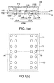
- Fig. 1(a) is a schematic sectional view of a plastic package in a preferred embodiment according to the present invention
- Fig. 1(b) is a bottom view of the plastic package shown in Fig. 1(a) taken from the side of external electrodes in the direction of the arrow AO in Fig. 1(a)
- Fig. 2 is a perspective view of the plastic package shown in Fig. 1, showing external electrodes and side surfaces
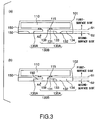
- Figs. 3(a) and 3(b) are schematic sectional views of plastic packages in modifications of the plastic package shown in Fig. 1
- Fig. 4(a) is a schematic plan view of a lead member in a preferred embodiment according to the present invention
- FIG. 4(b) is an enlarged perspective view of a portion B1 surrounded by dotted lines in Fig. 4(a)
- Figs. 5(a) to 5(g) are views of assistance in explaining a lead member fabricating method in a preferred embodiment according to the present invention
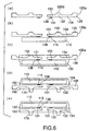
- Figs. 6(a) to 6(e) are views of assistance in explaining a method of fabricating the plastic package shown in Fig. 1.
- Fig. 1(a) is a sectional view taken on line A1-A2 in Fig. 1(b).
- Figs. 1 to 6 Shown in Figs. 1 to 6 are plastic packages 100, 101 and 102, a semiconductor IC chip 110, a terminal-side surface 110S, terminals (pads) 115, a lead member 130, terminal sections 130A, a terminal assembly 130B, a surface 130S, a lead member 130a, inner terminal parts 131, contact surfaces 131S of the inner terminal parts 131, outer terminal parts 132, contact surfaces 132S of the outer terminal parts 132, connecting parts 133, supporting parts 134, a frame 135, plated metal layers 138, a resin molding 150, external electrodes 170 of solder, a metal sheet 510, resist films 520, patterned resist films 521 and 522, and thin parts 530.
- the plastic package 100 in a preferred embodiment according to the present invention will be described with reference to Figs. 1 and 2.
- the plastic package 100 is formed by sealing the semiconductor IC chip 110 in the resin molding 150 with parts (contact surfaces 132S) of the outer terminal parts 132 exposed in the lower surface of the resin molding 150.
- the external electrodes 170 of solder to be used for connecting the semiconductor IC chip 100 to circuits formed on a wiring board or the like are attached to the exposed contact surfaces 132S of the outer terminal parts 132. Only portions of the lead member 130 in a region B2 demarcated by chain lines in Fig. 4(a) are sealed in the resin molding 150, and portions of the lead member 130 outside the region B2 are cut and separated from the former portions sealed in the resin molding 150.
- the plastic package 100 includes the semiconductor IC chip 110 sealed in the resin molding 150, and the terminal assembly 130B formed by separately arranging the terminal sections 130A.
- Each terminal section 130A has the inner terminal parts 131 to be electrically connected to the terminals 115 of the semiconductor IC chip 110, the outer terminal parts 132 to be connected to an external circuit, and the connecting parts 133 interconnecting the inner terminal parts 131 and the outer terminal parts 132, respectively.
- the contact surfaces 131S of the inner terminal parts 131 and the contact surfaces 132S of the outer terminal parts 132 face toward opposite directions, respectively.
- the inner terminal parts 131 and the connecting parts 133 are thin and the outer terminal parts 132 are thick.
- the contact surfaces 131S of the inner terminal parts 131 of each terminal section 130A are included in a plane S1.
- the plane S1 including the contact surfaces 131S of the inner terminal parts 131 of the terminal assembly 130B faces the terminal-side surface 110S on the side of the terminals 115 of the semiconductor IC chip 110.
- the terminals 115 of the semiconductor IC chip 110 are joined to or in contact with the contact surfaces 131S of the inner terminal parts 131 of the terminal assembly 130B. Thus, the terminals 115 of the semiconductor IC chip 110 are connected electrically to the inner terminal parts 131 of the terminal assembly 130B.
- the outer terminal parts 132 having the contact surfaces 132S of the terminal assembly 130B protrude from a plane including the inner terminal parts 131 and the connecting parts 133 in a direction away from the semiconductor IC chip 110.
- the connecting surface 132S of each outer terminal part 132 extends two-dimensionally in a plane S2 parallel to the terminal-side surface 110S on the side of the terminals 115 of the semiconductor IC chip 110.
- the supporting parts 134 of the lead member 130 shown in Fig. 4 remain in the plastic package 100.
- the terminal assembly 130B includes portions of the lead member 130 in the region B2 demarcated by chain lines in Fig. 4(a).
- first surfaces of the components of the terminal assembly 130B are portions of the surface 130S (Fig. 4(b)) of a metal sheet from which the lead member 130 is made and are included substantially in the plane S1.
- the contact surfaces 131S of the inner terminal parts 131 are portions of the surface 130S of the meal sheet and are included in the plane S1.
- the contact surfaces 131S of the inner terminal parts 131 of the terminal assembly 130B are coated with the plated metal layer 138, respectively.
- the plated metal layers 138 coating the contact surfaces 131S of the inner terminal parts 131 are joined to the terminals 115 of the semiconductor IC chip 110.
- the plated metal layers 138 are at least plated solder layers, plated gold layers, plated silver layers or plated palladium layers.
- the plated metal layers 138 are formed on the contact surfaces 131S of the inner terminal parts 131 of the terminal assembly 130B, and are joined to the terminals 115 of the semiconductor IC chip 110 by reflow soldering, metal-eutectic reaction or thermal compression bonding to connect the inner terminal parts 131 of the terminal assembly 130B to the terminals 115 of the semiconductor IC chip 110.
- the terminals 115 of the semiconductor IC chip 110 are arranged along a centerline extending in the middle between the opposite sides of the terminal-side surface 110S of the semiconductor IC chip 110.
- the inner terminal parts 131 are arranged in parallel to the centerline on the opposite sides of the centerline.
- the plastic package 100 shown in Fig. 1 is a CSP (chip size package) having dimensions substantially corresponding to those of the semiconductor IC chip 110.
- a plastic package in a modification of the plastic package 100 shown in Fig. 1 employs a lead member having a terminal assembly 130B including inner terminal parts 131 having connecting surfaces 131S respectively coated with connecting paste layers.
- the contact surfaces 131S of the inner terminal parts 131 of the terminal assembly 130B are connected to the terminals 115 of the semiconductor IC chip 110 with the bonding paste layers.
- the bonding paste layers are formed of a Pb-free bonding paste.
- the plastic package of the present invention is not limited to the plastic package 100 of a CSP type shown in Fig. 1.
- a plastic package 101 in a modification shown in Fig. 3(a) is not provided with any external electrodes corresponding to the external electrodes of solder of the plastic package 100 shown in Fig. 1.
- a plastic package 102 in another modification shown in Fig. 3(b) is provided with a lead member 130 having outer terminal parts 132 and supporting parts 134. Both the outer terminal parts 132 and the supporting parts 134 have the same thickness equal to that of a metal sheet from which the lead member 130 is formed.
- the plastic package 102 is superior in heat dissipating ability to the plastic package 100. However, cutting and separating a frame 135 of the lead member 130 is somewhat difficult.
- the terminal assembly 130B is formed of a Ni-Fe alloy, such as a Ni(42%)-Fe alloy, or a copper alloy.
- a lead member 130 in a preferred embodiment according to the present invention will be described with reference to Fig. 4.
- the region B2 demarcated by chain lines in Fig. 4(a) is sealed in a resin molding when forming a plastic package employing a lead member 130, and portions of the lead member 130 outside the region B2 are cut and removed.
- the lead member 130 has a generally flat shape and is employed in the plastic package 100 shown in Fig. 1.
- the contact surfaces 131s of inner terminal parts 131 are not coated with plated metal layers 138.
- the lead member 130 includes discrete terminal sections 130A, and a frame 135 surrounding and holding the terminal sections 130A.
- Each terminal section 130A has inner terminal parts 131 to be electrically connected to the terminals 115 of the semiconductor IC chip 110 as shown in Fig. 1, outer terminal parts 132 to be connected to an external circuit, and connecting parts 133 interconnecting the inner terminal parts 131 and the outer terminal parts 132, respectively.
- the contact surfaces 131S of the inner terminal parts 131 and the contact surfaces 132S of the outer terminal parts 132 face toward opposite directions, respectively.
- the inner terminal parts 131 and the connecting parts 133 are thin and the outer terminal parts 132 are thick.
- the contact surfaces 131S of the inner terminal parts 131 of each terminal section 130A are included in a plane S1.
- the frame 135 is connected to the outer terminal parts 132 by supporting parts 134 to hold the terminal sections 130A.
- the outer terminal parts 132 having the contact surfaces 132S of the terminal assembly 130B protrude from a plane including the inner terminal parts 131 and the connecting parts 133 in a direction away from the semiconductor IC chip 110.
- the connecting surface 132S of each outer terminal part 132 extends two-dimensionally in a plane S2 parallel to the terminal-side surface 110S on the side of the terminals 115 of the semiconductor IC chip 110.
- a surface of the lead member 130 facing the terminals of the semiconductor IC chip 110, i.e., a first surface in Fig. 1(a), is the surface 130S of a metal sheet from which the lead member 130 is made.
- the lead member 130 is formed of a Ni-Fe alloy, such as a Ni(42%)-Fe alloy, or a copper alloy.
- the lead member 30, similarly to ordinary lead frames, may be shaped by etching.
- a lead member 130 obtained by coating the contact surfaces 131S of the inner terminal parts 131 of the lead member 130 shown in Fig. 4 with a plated metal layer 138 for connecting the inner terminal parts 131 of the lead member 130 and the terminals 115 of the semiconductor IC chip 110 is employed in the plastic package 100 shown in Fig. 1.
- the plated metal layers for connecting the inner terminal parts of the lead member to the terminals of the semiconductor IC chip are at least plated solder layers, plated gold layers, plated silver layers, plated palladium layers or plated silver-tin layers.
- a lead member 130 similarly to the lead member 130 shown in Fig. 4, provided with inner terminal parts 131 having contact surfaces 131S coated with a paste layer for connecting the inner terminal parts 131 of the lead member 130 to the terminals 115 of the semiconductor IC chip 110.
- Fig. 5 shows only a section on line B3-B4 in Fig. 4(a) to facilitate understanding the explanation.
- a metal sheet 510 of about 0.2 mm in thickness of a 42-alloy (Ni(42%)-Fe alloy) or a copper alloy as shown in Fig. 5(a) is used for forming the lead member 130. Both the surfaces of the metal sheet 510 are degreased and cleaned. Then a photoresist is applied to both the surfaces of the metal sheet 510 in films and the films are dried to form photoresist layers 520 as shown in Fig. 5(b).
- Both the surfaces of the metal sheet 510 coated with the photoresist layers 520 are covered with masks of predetermined patterns, the photoresist layers 520 are exposed to light through the masks, the exposed photoresist layers 520 are developed to form etching masks 521 and 522 of predetermined patterns as shown in Fig. 5(c).
- Regions of one of the surfaces of the metal sheet 510 corresponding to the inner terminal parts, connecting parts and the supporting parts are not coated with the photoresist.
- casein resist containing potassium dichromate as a photosensitive agent or a liquid negative resist such as PMER® commercially available from Tokyo Ouka K.K., may be used.
- both the surfaces of the metal sheet 510 is etched by an etching process using the etching masks 521 and 522.
- portions of the metal sheet 510 corresponding to the regions of one of the surfaces of the metal sheet 510 are etched from only one of the surfaces of the metal sheet 510. This mode of etching is designated as "half-etching" in this description.
- Depths of etched portions in both the surfaces of the metal sheet 510 are adjusted to adjust the thickness of thin parts 530.
- an aqueous solution of ferric chloride is used as an etchant.
- the etchant is sprayed on both the surfaces of the metal sheet.
- Fig. 5(d) shows a state of the metal sheet 510 during the etching process.
- a portion of the metal sheet 510 between the opposite inner terminal parts 131 is removed, inner terminal parts 131, connecting parts 133 and supporting parts 134 are formed in a thickness smaller than that of the metal sheet 510, and outer terminal parts 132 and a frame 135 are formed in a thickness equal to that of the metal sheet 510 as shown in Fig. 5(e).
- a portion of the surface 510S of the metal sheet 510 forms one of the surfaces of each of the inner terminal parts 131, the connecting parts 133 and the supporting parts 134.
- the etching masks are removed as shown in Fig. 5(f) to obtain a lead member 130 as shown in Fig. 4.
- the contact surfaces of the inner terminal parts of the lead member 130 are plated to obtain a lead member 130a having the inner terminal parts having the contact Surfaces coated, respectively, with plated metal layers 138 as shown in Fig. 5(g) for the plastic package shown in Fig. 1.
- the plated metal layers 138 formed on the contact surfaces of the inner terminal parts 131 of the lead member 130 are at least plated solder layers, plated gold layers, plated silver layers or plated palladium layers.
- a photoresist mask is used to plate only the contact surfaces of the inner terminal parts 131.
- Connecting paste layers for connecting the inner terminal parts 131 and the terminals of the semiconductor IC chip may be formed on the contact surfaces of the inner terminal parts of the lead member 130 by a printing method or a dispense method to obtain the aforesaid lead member in the modification.
- the lead member 130a shown in Fig. 4 is fabricated by the method previously described with reference to Fig. 5 (Fig. 6(a)).
- a semiconductor IC chip 110 and the lead member 130a are disposed with the contact surfaces 131S of the inner terminal parts 131 of the terminal assembly 130B facing the terminal-side surface on the side of the terminals 115 of the semiconductor IC chip 110.
- the terminals 115 of the semiconductor IC chip 110 are joined to or in contact with the contact surfaces 131S of the inner terminal parts 131 of the terminal assembly 130B.
- the terminals 115 of the semiconductor IC chip 110 are connected electrically to the inner terminal parts 131 of the terminal assembly 130B by reflow soldering, metal-eutectic reaction or thermal compression bonding as shown in Fig. 6(b).
- the semiconductor IC chip 110 and the lead member 130a are sealed in a resin molding 150 with the outer terminal parts 132 exposed partly as shown in Fig. 6(c).
- the exposed contact surfaces 132S of the outer terminal parts 132 are subjected to a surface treatment, such as solder plating, and external electrodes 170, such as solder balls, are formed on the exposed surfaces 132S of the outer terminal parts 132 as shown in Fig. 6(d).
- a surface treatment such as solder plating
- external electrodes 170 such as solder balls
- the supporting parts 134 of the lead member 130 are cut by pressing to remove the frame 135 as shown in Fig. 6(e).
- the external electrodes 170 i.e., solder balls
- the external electrodes 170 may be formed by any method, such as a screen printing method using a solder paste or reflow soldering method, provided that the external electrodes 170 each of an amount of solder necessary for joining the plastic package to a wiring board.
- a plastic package in Example 1 was made, similarly to the plastic package shown in Fig. 1, by fabricating the lead member shown in Fig. 4 (Fig. 5(f)) by the lead member fabricating method shown in Fig. 5, and by the plastic package fabricating method shown in Fig. 6 using the lead member having inner terminal parts having the contact surfaces respectively coated with the plated metal layers (Fig. 6(g)).
- the lead member 130a was fabricated by the following method, which will be described with reference to Fig. 5.
- Both the surfaces of the metal sheet 510 coated with the photoresist layers 520 were covered with masks of predetermined patterns (photomasks), the photoresist layers 520 were exposed to light through the masks, the exposed photoresist layers 520 were developed to form etching masks 521 and 522 of predetermined patterns (Fig. 5(c)).
- Both the surfaces of the metal sheet 510 were etched by a spray etching method using a ferric chloride etchant and the etching masks 521 and 522 (Figs. 5(d) and 5(e)). After the completion of the etching process, the etching masks 521 and 522 were removed by an etching mask removing process using a proper alkaline remover, and the metal sheet 510 was cleaned to obtain a lead member 130 shown in Fig. 4 (Fig. 5(f)).
- the entire surface of the lead member 130 was coated with an electrodeposition resist film by an electrodeposition process, the electrodeposition resist film was exposed to light through a mask of a predetermined pattern corresponding to the pattern of plated metal layers to be formed on the contact surfaces 131S of the inner terminal parts 131, the exposed electrodeposition resist film was developed to form a plating mask of the electrodeposition resist having openings corresponding to the pattern of the plated meal layers. Then the lead member 130 coated with the plating mask was subjected to a solder plating process to form plated solder layers, i.e., plated metal layers, on portions of the contact surfaces 131S of the inner terminal parts 131 corresponding to the openings in the plating mask. Then, the plating mask was removed by a plating mask removing process using a proper remover to obtain a lead member 130a (Fig. 5(g)).
- a high-temperature solder (90% Pb) was used for solder plating.
- An electrodeposition liquid for forming the electrodeposition film, and the remover for removing the electrodeposition film are those represented by those for eagle process commercially available from Shipray.
- the inner terminal parts 131 of the lead member 130a (Fig. 6(a)) thus fabricated and the terminals 115, i.e., metal bumps, of the semiconductor IC chip 110 were bonded together with the plated solder layers 138 formed on the lead member 130 by flip-chip solder bonding to form an assembly of the semiconductor IC chip 110 and the lead member 130a (Fig. 6(b)).
- the assembly was sealed in a resin molding (Fig. 6(c)).
- the resin molding was formed by molding an epoxy resin in a predetermined mold.
- solder balls were attached to the outer terminal parts 132 to form external electrodes 170 (Fig. 6(d)).
- supporting parts 134 of the lead member 130a were cut by pressing to remove a frame 135 to complete a plastic package as shown in Fig. 1 (Fig. 6(e)).
- a lead member 130 shown in Fig. 4 was fabricated by processing a 0.15 mm thick metal sheet 510 of the 42-alloy (Ni(42%)-Fe alloy) by the lead member fabricating method shown in Fig. 5.
- a lead member 130a was obtained by coating the contact surfaces of inner terminal parts of the lead member 130 with films of a conductive paste by a screen printing method (Figs. 5(g) and 6(a)).
- An Ag-Sn paste was used as the conductive paste.
- the resin molding was formed by molding an epoxy resin in a predetermined mold.
- solder balls were attached to the outer terminal parts 132 to form external electrodes 170 (Fig. 6(d)).
- supporting parts 134 of the lead member 130a were cut by pressing to remove a frame 135 to complete a plastic package as shown in Fig. 1 (Fig. 6(e)).
- the present invention provides a plastic package capable of increasing the ratio of the size of the semiconductor IC chip to the that of the plastic package, meeting demand for miniaturization, requiring a small mounting area on a wiring board, and capable of increasing packaging density.
Landscapes
- Lead Frames For Integrated Circuits (AREA)
- Structures Or Materials For Encapsulating Or Coating Semiconductor Devices Or Solid State Devices (AREA)
Abstract
Description
Claims (18)
- A resin-encapsulated package having terminals including some exposed terminals, said resin-encapsulated package comprising:a semiconductor IC chip sealed in a resin molding, anda lead member having an arrangement of a plurality of discrete terminal sections;
wherein each of the terminal sections has inner terminal parts to be electrically connected to terminals of the semiconductor IC chip, outer terminal parts to be connected to external circuits, and connecting parts interconnecting the inner and the outer terminal parts,the inner and the outer terminal parts are formed such that contact surfaces of the inner terminal parts and those of the outer terminal parts facing toward opposite directions, respectively,the inner terminal parts and the connecting parts are thin, and the outer terminal parts are thick,the contact surfaces of the inner terminal parts of the terminal sections are flush with each other,a terminal-side surface of the semiconductor IC chip on the side of the terminals faces a surface of the lead member on the side of the contact surfaces of the inner terminal parts,the terminals of the semiconductor IC chip are joined to or in contact with the contact surfaces of the inner terminal parts of the lead member, and the terminals of the semiconductor IC chip are connected electrically to the inner terminal parts of the lead member. - The resin-encapsulated package according to claim 1,
wherein the terminals of the semiconductor IC chip are provided with protruding electrodes, and the protruding electrodes are joined to or in contact with the contact surfaces of the inner terminal parts. - The resin-encapsulated package according to claim 1,
wherein the contact surfaces of the inner terminal parts are coated with connecting plated metal layers, respectively, and the terminals of the semiconductor IC chip and the inner terminal parts of the lead member are connected electrically through the plated metal layers. - The resin-encapsulated package according to claim 3,
wherein the plated metal layers are at least plated solder layers, plated gold layers, plated silver layers or plated palladium layers. - The resin-encapsulated package according to claim 3,
wherein the plated metal layers are formed on only parts of the contact surfaces of the inner terminal parts facing the terminals of the semiconductor IC chip. - The resin-encapsulated package according to claim 1,
wherein the contact surfaces of the inner terminal parts are coated with conductive paste layers, respectively, the terminals of the semiconductor IC chip and the inner terminal parts of the lead member are connected electrically through the conductive paste layer. - The resin-encapsulated package according to claim 1,
wherein at least portions of the outer terminal parts are exposed on the resin molding or external electrodes of solder or the like are formed on the surfaces of the exposed portions of the outer terminal parts. - A lead member for a substantially flat resin-encapsulated package including a semiconductor IC chip, said lead member comprising:a plurality of discrete terminal sections, anda frame surrounding and holding the plurality of discrete terminal sections;
wherein each of the terminal sections has inner terminal parts to be electrically connected to terminals of the semiconductor IC chip, outer terminal parts to be connected to external circuits, and connecting parts interconnecting the inner and the outer terminal parts,the inner and the outer terminal parts are formed such that contact surfaces of the inner terminal parts and those of the outer contact parts facing toward opposite directions, respectively,the inner terminal parts and the connecting parts are thin, and the outer terminal parts are thick,contact surfaces of the inner terminal parts of the terminal sections are flush with each other, andthe frame is provided with supporting parts other than the connecting parts, and the supporting parts are connected to the outer terminal parts, respectively. - The resin-encapsulated package according to claim 8,
wherein the lead member is formed by processing a metal sheet by a half-etching method. - The resin-encapsulated package according to claim 8,
wherein contact surfaces of inner terminal parts are coated with connecting plated metal layers, respectively, and the terminals of the semiconductor IC chip and the inner terminal parts of the lead member are connected electrically through the plated metal layers, respectively, when assembling the lead member and the semiconductor IC chip. - The resin-encapsulated package according to claim 10,
wherein the plated metal layers are at least plated solder layers, plated gold layers, plated silver layers or plated palladium layers. - The resin-encapsulated package according to claim 8,
wherein the contact surfaces of the inner terminal parts are coated with conductive paste layers, respectively, and the terminals of the semiconductor IC chip and the inner terminal parts of the lead member are connected electrically through the conductive paste layers, respectively. - The resin-encapsulated package according to claim 12,
wherein, the paste layers are formed of a Pb-free paste. - A lead member fabricating method of fabricating a lead member for a substantially flat resin-encapsulated package including a semiconductor IC chip, having a plurality of discrete terminal sections, and a frame surrounding and holding the plurality of discrete terminal sections, wherein each of the terminal sections has inner terminal parts to be electrically connected to terminals of the semiconductor IC chip, outer terminal parts to be connected to external circuits, and connecting parts interconnecting the inner and the outer terminal parts, respectively, the inner and the outer terminal part are formed such that contact surfaces of the inner terminal parts and those of the outer terminal parts facing toward opposite directions, respectively, the inner terminal parts and the connecting parts are thin, the outer terminal parts are thick, the contact surfaces of the inner terminal parts of the terminal sections are flush with each other, the frame is provided with supporting parts other than the connecting parts, and the supporting parts are connected to the outer terminal parts;
said lead member fabricating method comprising processing a metal sheet by a half-etching method so that surfaces of the inner terminal parts, the connecting parts and the supporting parts are portions of one of the surfaces of the metal sheet, the inner terminal parts, the connecting parts and the supporting parts have a thickness smaller than that of the metal sheet, and the outer terminal parts have a thickness equal to that of the metal sheet. - The lead member fabricating method according to claim 14, wherein plated metal layers are formed on the contact surfaces of the inner terminal parts.
- The lead member fabricating method according to claim 15, wherein the plated metal layers are formed by coating the surface of the lead member with a photoresist film, patterning the photoresist film to form openings in parts thereof corresponding to the contact surfaces of the inner terminal parts so that the contact surfaces of the inner terminal parts are exposed, and subjecting the lead member to a plating process using the patterned photoresist film as a mask to plate the exposed contact surfaces of the inner terminal parts.
- The lead member according to claim 14, wherein the contact surfaces of the inner terminal parts are coated with paste layers, respectively.
- The lead member according to claim 17, wherein the paste layers are formed by a printing method or a dispense method.
Applications Claiming Priority (5)
| Application Number | Priority Date | Filing Date | Title |
|---|---|---|---|
| JP2000068290 | 2000-03-13 | ||
| JP2000068290 | 2000-03-13 | ||
| JP2000166377A JP4549491B2 (en) | 2000-03-13 | 2000-06-02 | Resin-sealed semiconductor device |
| JP2000166377 | 2000-06-02 | ||
| PCT/JP2001/001985 WO2001069678A1 (en) | 2000-03-13 | 2001-03-13 | Resin-sealed semiconductor device, circuit member used for the device, and method of manufacturing the circuit member |
Publications (2)
| Publication Number | Publication Date |
|---|---|
| EP1189279A1 true EP1189279A1 (en) | 2002-03-20 |
| EP1189279A4 EP1189279A4 (en) | 2006-04-12 |
Family
ID=26587288
Family Applications (1)
| Application Number | Title | Priority Date | Filing Date |
|---|---|---|---|
| EP01912332A Withdrawn EP1189279A4 (en) | 2000-03-13 | 2001-03-13 | SEMICONDUCTOR SEMICONDUCTOR DEVICE WITH RESIN ENVELOPE, CIRCUIT MEMBER FOR THIS DEVICE, AND METHOD FOR MANUFACTURING THE CIRCUIT MEMBER |
Country Status (5)
| Country | Link |
|---|---|
| US (3) | US6828688B2 (en) |
| EP (1) | EP1189279A4 (en) |
| JP (1) | JP4549491B2 (en) |
| KR (1) | KR100811338B1 (en) |
| WO (1) | WO2001069678A1 (en) |
Cited By (7)
| Publication number | Priority date | Publication date | Assignee | Title |
|---|---|---|---|---|
| DE10147376A1 (en) * | 2001-09-26 | 2003-04-24 | Infineon Technologies Ag | Electronic component used in electronic devices comprises a plastic housing and a metallic support arranged in the housing with a semiconductor chip arranged on the metallic support using Flip-Chip technology |
| DE10147375A1 (en) * | 2001-09-26 | 2003-04-24 | Infineon Technologies Ag | Electronic component used in electronic devices comprises a semiconductor chip arranged on a chip island and embedded in a plastic housing within which bond connections extend |
| EP1659628A1 (en) * | 2004-11-23 | 2006-05-24 | Optium Care International Tech. Inc. | High lead density electronic device |
| DE102006006825A1 (en) * | 2006-02-14 | 2007-08-23 | Infineon Technologies Ag | Semiconductor component e.g. ball grid array semiconductor component, has semiconductor chip with protective casing, and soldering ball arranged in recess of electrical insulating layer and connected with connecting carrier |
| WO2008088291A1 (en) * | 2007-01-16 | 2008-07-24 | Infineon Technologies Ag | Method of semiconductor packaging and/or a semiconductor package |
| EP1938382A4 (en) * | 2005-08-22 | 2012-09-05 | Texas Instruments Inc | HIGH CURRENT SEMICONDUCTOR DEVICE SYSTEM HAVING LOW RESISTANCE AND LOW INDUCTANCE |
| USRE46466E1 (en) | 2005-09-01 | 2017-07-04 | Texas Instruments Incorporated | Method for fabricating low resistance, low inductance interconnections in high current semiconductor devices |
Families Citing this family (25)
| Publication number | Priority date | Publication date | Assignee | Title |
|---|---|---|---|---|
| JP4549491B2 (en) * | 2000-03-13 | 2010-09-22 | 大日本印刷株式会社 | Resin-sealed semiconductor device |
| TWM253056U (en) * | 2004-02-13 | 2004-12-11 | Optimum Care Int Tech Inc | Compact chip packaging structure |
| US8502362B2 (en) * | 2011-08-16 | 2013-08-06 | Advanced Analogic Technologies, Incorporated | Semiconductor package containing silicon-on-insulator die mounted in bump-on-leadframe manner to provide low thermal resistance |
| CN102983248B (en) | 2006-06-02 | 2017-11-14 | 日立化成株式会社 | Optical semiconductor package for mounting and use its optical semiconductor device |
| US8604624B2 (en) * | 2008-03-19 | 2013-12-10 | Stats Chippac Ltd. | Flip chip interconnection system having solder position control mechanism |
| US20110042794A1 (en) * | 2008-05-19 | 2011-02-24 | Tung-Hsien Hsieh | Qfn semiconductor package and circuit board structure adapted for the same |
| US7786557B2 (en) * | 2008-05-19 | 2010-08-31 | Mediatek Inc. | QFN Semiconductor package |
| US8269324B2 (en) * | 2008-07-11 | 2012-09-18 | Stats Chippac Ltd. | Integrated circuit package system with chip on lead |
| JP5271949B2 (en) | 2009-09-29 | 2013-08-21 | ルネサスエレクトロニクス株式会社 | Semiconductor device |
| US9076776B1 (en) * | 2009-11-19 | 2015-07-07 | Altera Corporation | Integrated circuit package with stand-off legs |
| US8193620B2 (en) * | 2010-02-17 | 2012-06-05 | Analog Devices, Inc. | Integrated circuit package with enlarged die paddle |
| CN101840902B (en) * | 2010-04-30 | 2011-06-15 | 江苏长电科技股份有限公司 | Direct chip placing lead frame structure and production method thereof |
| US9123737B2 (en) * | 2010-09-21 | 2015-09-01 | Texas Instruments Incorporated | Chip to dielectric waveguide interface for sub-millimeter wave communications link |
| CN102005432B (en) * | 2010-09-30 | 2012-03-28 | 江苏长电科技股份有限公司 | Packaging structure with four pin-less sides and packaging method thereof |
| TWI416637B (en) | 2010-10-15 | 2013-11-21 | 南茂科技股份有限公司 | Chip package structure and chip packaging method |
| CN102468187A (en) * | 2010-11-05 | 2012-05-23 | 南茂科技股份有限公司 | Chip packaging structure and chip packaging method |
| CN102394232A (en) * | 2011-11-29 | 2012-03-28 | 杭州矽力杰半导体技术有限公司 | A lead frame and chip flip-chip packaging device using the same |
| KR101965127B1 (en) * | 2012-10-29 | 2019-04-04 | 삼성전자 주식회사 | Semiconductor package and method for fabricating the same |
| CN104465593B (en) * | 2014-11-13 | 2018-10-19 | 苏州日月新半导体有限公司 | Semiconductor package and packaging method |
| JP6760729B2 (en) * | 2014-12-11 | 2020-09-23 | 共同紙工株式会社 | Bag body and bag body |
| JP2017147272A (en) | 2016-02-15 | 2017-08-24 | ローム株式会社 | Semiconductor device and method for manufacturing the same, and lead frame intermediate used for manufacturing the semiconductor device |
| JP7024349B2 (en) | 2017-11-24 | 2022-02-24 | セイコーエプソン株式会社 | Sensor units, sensor unit manufacturing methods, inertial measurement units, electronic devices, and mobiles |
| US11069600B2 (en) | 2019-05-24 | 2021-07-20 | Infineon Technologies Ag | Semiconductor package with space efficient lead and die pad design |
| JP6709313B1 (en) * | 2019-05-31 | 2020-06-10 | アオイ電子株式会社 | Semiconductor device and method of manufacturing semiconductor device |
| JPWO2023095681A1 (en) * | 2021-11-24 | 2023-06-01 |
Family Cites Families (23)
| Publication number | Priority date | Publication date | Assignee | Title |
|---|---|---|---|---|
| US4633582A (en) * | 1985-08-14 | 1987-01-06 | General Instrument Corporation | Method for assembling an optoisolator and leadframe therefor |
| JPS6254048A (en) * | 1985-09-02 | 1987-03-09 | Hitachi Metals Ltd | Copper alloy for lead frame |
| JP2619123B2 (en) * | 1990-07-19 | 1997-06-11 | 株式会社東芝 | Semiconductor manufacturing equipment |
| JPH08222681A (en) * | 1995-02-14 | 1996-08-30 | Toshiba Corp | Resin-sealed semiconductor device |
| JPH08306853A (en) * | 1995-05-09 | 1996-11-22 | Fujitsu Ltd | Semiconductor device, method of manufacturing the same, and method of manufacturing lead frame |
| JPH0917910A (en) * | 1995-06-28 | 1997-01-17 | Hitachi Ltd | Semiconductor device, manufacturing method thereof, inspection method, and mounting substrate |
| JP3465098B2 (en) * | 1995-07-04 | 2003-11-10 | 大日本印刷株式会社 | Lead frame and PGA type resin-sealed semiconductor device |
| JPH09312374A (en) * | 1996-05-24 | 1997-12-02 | Sony Corp | Semiconductor package and manufacturing method thereof |
| JP3793628B2 (en) * | 1997-01-20 | 2006-07-05 | 沖電気工業株式会社 | Resin-sealed semiconductor device |
| JPH1154663A (en) * | 1997-08-04 | 1999-02-26 | Dainippon Printing Co Ltd | Resin-sealed semiconductor device, circuit member used therefor, and method of manufacturing circuit member |
| JPH1174411A (en) * | 1997-08-29 | 1999-03-16 | Dainippon Printing Co Ltd | Resin-sealed semiconductor device and circuit member used for the same |
| JPH11251504A (en) * | 1998-02-27 | 1999-09-17 | Nec Kansai Ltd | Electronic component and method of manufacturing the same |
| JP3173459B2 (en) * | 1998-04-21 | 2001-06-04 | 日本電気株式会社 | Method for manufacturing semiconductor device |
| TW396559B (en) * | 1998-07-24 | 2000-07-01 | Siliconware Precision Industries Co Ltd | The semiconductor device having heat dissipating structure |
| JP3169919B2 (en) * | 1998-12-21 | 2001-05-28 | 九州日本電気株式会社 | Ball grid array type semiconductor device and method of manufacturing the same |
| JP2001077232A (en) * | 1999-09-06 | 2001-03-23 | Mitsubishi Electric Corp | Semiconductor device and method of manufacturing the same |
| JP3994262B2 (en) * | 1999-10-04 | 2007-10-17 | セイコーエプソン株式会社 | Semiconductor device and manufacturing method thereof, circuit board, and electronic apparatus |
| JP2001230360A (en) * | 2000-02-18 | 2001-08-24 | Hitachi Ltd | Semiconductor integrated circuit device and method of manufacturing the same |
| JP4549491B2 (en) * | 2000-03-13 | 2010-09-22 | 大日本印刷株式会社 | Resin-sealed semiconductor device |
| JP3683179B2 (en) * | 2000-12-26 | 2005-08-17 | 松下電器産業株式会社 | Semiconductor device and manufacturing method thereof |
| TW523887B (en) * | 2001-11-15 | 2003-03-11 | Siliconware Precision Industries Co Ltd | Semiconductor packaged device and its manufacturing method |
| US7154186B2 (en) * | 2004-03-18 | 2006-12-26 | Fairchild Semiconductor Corporation | Multi-flip chip on lead frame on over molded IC package and method of assembly |
| US7217991B1 (en) * | 2004-10-22 | 2007-05-15 | Amkor Technology, Inc. | Fan-in leadframe semiconductor package |
-
2000
- 2000-06-02 JP JP2000166377A patent/JP4549491B2/en not_active Expired - Lifetime
-
2001
- 2001-03-13 KR KR1020017014407A patent/KR100811338B1/en not_active Expired - Lifetime
- 2001-03-13 EP EP01912332A patent/EP1189279A4/en not_active Withdrawn
- 2001-03-13 WO PCT/JP2001/001985 patent/WO2001069678A1/en not_active Ceased
- 2001-03-13 US US09/959,660 patent/US6828688B2/en not_active Expired - Lifetime
-
2004
- 2004-10-05 US US10/957,683 patent/US7045906B2/en not_active Expired - Lifetime
-
2006
- 2006-02-28 US US11/362,784 patent/US7307347B2/en not_active Expired - Lifetime
Cited By (11)
| Publication number | Priority date | Publication date | Assignee | Title |
|---|---|---|---|---|
| DE10147376A1 (en) * | 2001-09-26 | 2003-04-24 | Infineon Technologies Ag | Electronic component used in electronic devices comprises a plastic housing and a metallic support arranged in the housing with a semiconductor chip arranged on the metallic support using Flip-Chip technology |
| DE10147375A1 (en) * | 2001-09-26 | 2003-04-24 | Infineon Technologies Ag | Electronic component used in electronic devices comprises a semiconductor chip arranged on a chip island and embedded in a plastic housing within which bond connections extend |
| DE10147375B4 (en) * | 2001-09-26 | 2006-06-08 | Infineon Technologies Ag | Electronic component with a semiconductor chip and method for producing the same |
| DE10147376B4 (en) * | 2001-09-26 | 2009-01-15 | Infineon Technologies Ag | Electronic component and leadframe and method for producing the same |
| EP1659628A1 (en) * | 2004-11-23 | 2006-05-24 | Optium Care International Tech. Inc. | High lead density electronic device |
| EP1938382A4 (en) * | 2005-08-22 | 2012-09-05 | Texas Instruments Inc | HIGH CURRENT SEMICONDUCTOR DEVICE SYSTEM HAVING LOW RESISTANCE AND LOW INDUCTANCE |
| USRE46466E1 (en) | 2005-09-01 | 2017-07-04 | Texas Instruments Incorporated | Method for fabricating low resistance, low inductance interconnections in high current semiconductor devices |
| USRE48420E1 (en) | 2005-09-01 | 2021-02-02 | Texas Instruments Incorporated | Method for fabricating low resistance, low inductance interconnections in high current semiconductor devices |
| DE102006006825A1 (en) * | 2006-02-14 | 2007-08-23 | Infineon Technologies Ag | Semiconductor component e.g. ball grid array semiconductor component, has semiconductor chip with protective casing, and soldering ball arranged in recess of electrical insulating layer and connected with connecting carrier |
| WO2008088291A1 (en) * | 2007-01-16 | 2008-07-24 | Infineon Technologies Ag | Method of semiconductor packaging and/or a semiconductor package |
| US7939381B2 (en) | 2007-01-16 | 2011-05-10 | Infineon Technologies Ag | Method of semiconductor packaging and/or a semiconductor package |
Also Published As
| Publication number | Publication date |
|---|---|
| WO2001069678A1 (en) | 2001-09-20 |
| KR100811338B1 (en) | 2008-03-07 |
| US20060138620A1 (en) | 2006-06-29 |
| US20050046045A1 (en) | 2005-03-03 |
| JP4549491B2 (en) | 2010-09-22 |
| US7307347B2 (en) | 2007-12-11 |
| US20020158347A1 (en) | 2002-10-31 |
| KR20020005745A (en) | 2002-01-17 |
| US7045906B2 (en) | 2006-05-16 |
| JP2001332675A (en) | 2001-11-30 |
| EP1189279A4 (en) | 2006-04-12 |
| US6828688B2 (en) | 2004-12-07 |
Similar Documents
| Publication | Publication Date | Title |
|---|---|---|
| US7045906B2 (en) | Resin-encapsulated package, lead member for the same and method of fabricating the lead member | |
| US6359221B1 (en) | Resin sealed semiconductor device, circuit member for use therein | |
| US6025640A (en) | Resin-sealed semiconductor device, circuit member for use therein and method of manufacturing resin-sealed semiconductor device | |
| US7704799B2 (en) | Method of manufacturing wiring substrate | |
| EP1213755A2 (en) | Fabrication process of semiconductor package and semiconductor package | |
| JPH098207A (en) | Resin-sealed semiconductor device | |
| JPH08125066A (en) | Resin-sealed semiconductor device, lead frame used therefor, and method of manufacturing resin-sealed semiconductor device | |
| KR20010083204A (en) | Semiconductor device and method for fabricating the same | |
| KR100630581B1 (en) | Manufacturing method of carrier substrate for producing semiconductor device, and semiconductor device and manufacturing method thereof | |
| JP2000091488A (en) | Resin-sealed semiconductor device and circuit member used for the same | |
| JPH10335566A (en) | Resin-sealed semiconductor device, circuit member used therefor, and method of manufacturing resin-sealed semiconductor device | |
| JP5850347B2 (en) | Resin-sealed semiconductor device | |
| JPH11163024A (en) | Semiconductor device, lead frame for assembling the same, and method of manufacturing semiconductor device | |
| JP4357728B2 (en) | Resin-sealed semiconductor device | |
| JPH1154663A (en) | Resin-sealed semiconductor device, circuit member used therefor, and method of manufacturing circuit member | |
| JP2001007274A (en) | Resin-sealed semiconductor device, circuit member used therefor, and method of manufacturing circuit member | |
| JPH1126648A (en) | Semiconductor device and its lead frame | |
| JPH1174411A (en) | Resin-sealed semiconductor device and circuit member used for the same | |
| JP4176092B2 (en) | Resin-sealed semiconductor device and manufacturing method thereof | |
| JPH10154766A (en) | Semiconductor package manufacturing method and semiconductor package | |
| JPH1116947A (en) | Semiconductor package and manufacturing method thereof | |
| JP3908695B2 (en) | Resin-sealed semiconductor device | |
| JP3802500B2 (en) | Lead frame | |
| JP2005260271A (en) | Circuit members for resin-encapsulated semiconductor devices | |
| JPH11135523A (en) | Semiconductor package manufacturing method |
Legal Events
| Date | Code | Title | Description |
|---|---|---|---|
| PUAI | Public reference made under article 153(3) epc to a published international application that has entered the european phase |
Free format text: ORIGINAL CODE: 0009012 |
|
| 17P | Request for examination filed |
Effective date: 20011122 |
|
| AK | Designated contracting states |
Kind code of ref document: A1 Designated state(s): AT BE CH CY DE DK ES FI FR GB GR IE IT LI LU MC NL PT SE TR |
|
| RBV | Designated contracting states (corrected) |
Designated state(s): DE FR IT |
|
| A4 | Supplementary search report drawn up and despatched |
Effective date: 20060224 |
|
| 17Q | First examination report despatched |
Effective date: 20070212 |
|
| GRAP | Despatch of communication of intention to grant a patent |
Free format text: ORIGINAL CODE: EPIDOSNIGR1 |
|
| RIC1 | Information provided on ipc code assigned before grant |
Ipc: H01L 23/495 20060101ALI20130201BHEP Ipc: H01L 23/31 20060101AFI20130201BHEP |
|
| STAA | Information on the status of an ep patent application or granted ep patent |
Free format text: STATUS: THE APPLICATION IS DEEMED TO BE WITHDRAWN |
|
| 18D | Application deemed to be withdrawn |
Effective date: 20130711 |