EP1187215A2 - Vertikale nichtflüchtige Halbleiter-Speicherzelle sowie Verfahren zu deren Herstellung - Google Patents
Vertikale nichtflüchtige Halbleiter-Speicherzelle sowie Verfahren zu deren Herstellung Download PDFInfo
- Publication number
- EP1187215A2 EP1187215A2 EP01119172A EP01119172A EP1187215A2 EP 1187215 A2 EP1187215 A2 EP 1187215A2 EP 01119172 A EP01119172 A EP 01119172A EP 01119172 A EP01119172 A EP 01119172A EP 1187215 A2 EP1187215 A2 EP 1187215A2
- Authority
- EP
- European Patent Office
- Prior art keywords
- trench
- layer
- semiconductor memory
- memory cell
- volatile semiconductor
- Prior art date
- Legal status (The legal status is an assumption and is not a legal conclusion. Google has not performed a legal analysis and makes no representation as to the accuracy of the status listed.)
- Withdrawn
Links
- 239000004065 semiconductor Substances 0.000 title claims abstract description 95
- 238000004519 manufacturing process Methods 0.000 title claims abstract description 9
- 238000000034 method Methods 0.000 title claims description 36
- 239000000463 material Substances 0.000 claims abstract description 34
- 239000000945 filler Substances 0.000 claims abstract description 14
- 230000008569 process Effects 0.000 claims description 27
- 239000000758 substrate Substances 0.000 claims description 25
- 229910021420 polycrystalline silicon Inorganic materials 0.000 claims description 12
- 229920005591 polysilicon Polymers 0.000 claims description 12
- 238000009413 insulation Methods 0.000 claims description 7
- 229910044991 metal oxide Inorganic materials 0.000 claims description 4
- 150000004706 metal oxides Chemical class 0.000 claims description 4
- 229910021332 silicide Inorganic materials 0.000 claims description 4
- FVBUAEGBCNSCDD-UHFFFAOYSA-N silicide(4-) Chemical compound [Si-4] FVBUAEGBCNSCDD-UHFFFAOYSA-N 0.000 claims description 4
- 239000010410 layer Substances 0.000 claims 39
- 239000002344 surface layer Substances 0.000 claims 1
- 230000014759 maintenance of location Effects 0.000 abstract description 16
- 230000008878 coupling Effects 0.000 abstract description 12
- 238000010168 coupling process Methods 0.000 abstract description 12
- 238000005859 coupling reaction Methods 0.000 abstract description 12
- 230000015654 memory Effects 0.000 description 12
- 238000005530 etching Methods 0.000 description 6
- 239000003990 capacitor Substances 0.000 description 5
- 238000007667 floating Methods 0.000 description 5
- 230000003071 parasitic effect Effects 0.000 description 5
- 238000002955 isolation Methods 0.000 description 3
- -1 MoSi Chemical compound 0.000 description 2
- 229910004298 SiO 2 Inorganic materials 0.000 description 2
- 230000008901 benefit Effects 0.000 description 2
- 230000015572 biosynthetic process Effects 0.000 description 2
- 239000011231 conductive filler Substances 0.000 description 2
- 238000010586 diagram Methods 0.000 description 2
- 230000006872 improvement Effects 0.000 description 2
- 150000004767 nitrides Chemical class 0.000 description 2
- 230000003647 oxidation Effects 0.000 description 2
- 238000007254 oxidation reaction Methods 0.000 description 2
- 230000002787 reinforcement Effects 0.000 description 2
- 229910018072 Al 2 O 3 Inorganic materials 0.000 description 1
- 229910001218 Gallium arsenide Inorganic materials 0.000 description 1
- 229910016006 MoSi Inorganic materials 0.000 description 1
- 229910000577 Silicon-germanium Inorganic materials 0.000 description 1
- 229910010413 TiO 2 Inorganic materials 0.000 description 1
- 230000002411 adverse Effects 0.000 description 1
- 239000000969 carrier Substances 0.000 description 1
- 239000002131 composite material Substances 0.000 description 1
- 239000004020 conductor Substances 0.000 description 1
- 238000012217 deletion Methods 0.000 description 1
- 230000037430 deletion Effects 0.000 description 1
- 230000001419 dependent effect Effects 0.000 description 1
- 230000008021 deposition Effects 0.000 description 1
- 238000009792 diffusion process Methods 0.000 description 1
- 239000012777 electrically insulating material Substances 0.000 description 1
- 238000005516 engineering process Methods 0.000 description 1
- 230000002349 favourable effect Effects 0.000 description 1
- 230000006870 function Effects 0.000 description 1
- 238000002347 injection Methods 0.000 description 1
- 239000007924 injection Substances 0.000 description 1
- 230000000873 masking effect Effects 0.000 description 1
- 230000007246 mechanism Effects 0.000 description 1
- 230000006386 memory function Effects 0.000 description 1
- 229910003465 moissanite Inorganic materials 0.000 description 1
- 230000009467 reduction Effects 0.000 description 1
- 229910010271 silicon carbide Inorganic materials 0.000 description 1
Images




Classifications
-
- H—ELECTRICITY
- H10—SEMICONDUCTOR DEVICES; ELECTRIC SOLID-STATE DEVICES NOT OTHERWISE PROVIDED FOR
- H10B—ELECTRONIC MEMORY DEVICES
- H10B41/00—Electrically erasable-and-programmable ROM [EEPROM] devices comprising floating gates
- H10B41/30—Electrically erasable-and-programmable ROM [EEPROM] devices comprising floating gates characterised by the memory core region
-
- H—ELECTRICITY
- H10—SEMICONDUCTOR DEVICES; ELECTRIC SOLID-STATE DEVICES NOT OTHERWISE PROVIDED FOR
- H10D—INORGANIC ELECTRIC SEMICONDUCTOR DEVICES
- H10D30/00—Field-effect transistors [FET]
- H10D30/60—Insulated-gate field-effect transistors [IGFET]
- H10D30/68—Floating-gate IGFETs
-
- H—ELECTRICITY
- H10—SEMICONDUCTOR DEVICES; ELECTRIC SOLID-STATE DEVICES NOT OTHERWISE PROVIDED FOR
- H10B—ELECTRONIC MEMORY DEVICES
- H10B41/00—Electrically erasable-and-programmable ROM [EEPROM] devices comprising floating gates
- H10B41/30—Electrically erasable-and-programmable ROM [EEPROM] devices comprising floating gates characterised by the memory core region
- H10B41/35—Electrically erasable-and-programmable ROM [EEPROM] devices comprising floating gates characterised by the memory core region with a cell select transistor, e.g. NAND
-
- H—ELECTRICITY
- H10—SEMICONDUCTOR DEVICES; ELECTRIC SOLID-STATE DEVICES NOT OTHERWISE PROVIDED FOR
- H10B—ELECTRONIC MEMORY DEVICES
- H10B69/00—Erasable-and-programmable ROM [EPROM] devices not provided for in groups H10B41/00 - H10B63/00, e.g. ultraviolet erasable-and-programmable ROM [UVEPROM] devices
-
- H—ELECTRICITY
- H10—SEMICONDUCTOR DEVICES; ELECTRIC SOLID-STATE DEVICES NOT OTHERWISE PROVIDED FOR
- H10B—ELECTRONIC MEMORY DEVICES
- H10B12/00—Dynamic random access memory [DRAM] devices
- H10B12/01—Manufacture or treatment
- H10B12/02—Manufacture or treatment for one transistor one-capacitor [1T-1C] memory cells
- H10B12/03—Making the capacitor or connections thereto
- H10B12/038—Making the capacitor or connections thereto the capacitor being in a trench in the substrate
-
- H—ELECTRICITY
- H10—SEMICONDUCTOR DEVICES; ELECTRIC SOLID-STATE DEVICES NOT OTHERWISE PROVIDED FOR
- H10B—ELECTRONIC MEMORY DEVICES
- H10B12/00—Dynamic random access memory [DRAM] devices
- H10B12/01—Manufacture or treatment
- H10B12/09—Manufacture or treatment with simultaneous manufacture of the peripheral circuit region and memory cells
Definitions
- the present invention relates to a vertical non-volatile semiconductor memory cell and an associated one Manufacturing process and in particular on an EPROM, EEPROM and FLASH EEPROM memory cells with a small footprint.
- Rewritable non-volatile semiconductor memory cells are becoming increasingly important in highly integrated circuits, since they are used, for example, in chip cards, multimedia cards and so-called smart cards changeable data over a long Period and without using a power supply can save.
- the different applications lead to different requirement profiles, the different require technological realizations.
- embedded non-volatile Memory where the non-volatile memory function at the same time with other functions taking into account their Requirement profiles are realized on the same chip.
- Semiconductor memory cells usually consist of one Semiconductor substrate, an insulating tunnel oxide layer, one Floating gate layer or charge storage layer, one insulating dielectric layer and a conductive control layer, which on the surface of the semiconductor substrate are trained.
- To store information Charges from a channel region formed in the semiconductor substrate over the tunnel oxide layer into the floating gate layer brought in.
- Procedure for loading into the floating gate layer for example, are hotter injection Load carriers and Fowler-Nordheim tunnels.
- a disadvantage of such conventional non-volatile semiconductor memory cells is the relatively high one Space requirement, which is particularly due to training of the surface of the semiconductor substrate.
- the space requirement cannot be known as with logic technologies reduce by scaling or shrinking, since the minimal structure sizes are largely due to the voltages required due to the physical mechanism are set for programming and deleting.
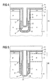
- FIG. 1 shows a sectional view of such a vertical non-volatile semiconductor memory cell, as is known for example from the publication WO97 / 02599.
- a semiconductor layer 200 which has, for example, a weakly doped p region 100, a p-doped well 110 and a heavily doped n + region 120, is used in the semiconductor substrate 200 by means of an auxiliary layer 130 and a mask layer (not shown) Trench 140 is formed, on the bottom of which another heavily doped n + region 150 is formed.
- the heavily doped n + regions 150 and 120 here represent so-called drain and source regions of the vertical non-volatile semiconductor memory cell.
- a tunnel oxide layer 160 is formed on the walls and on the bottom of the trench 140 as a dielectric layer. Adjoining this is the floating gate layer 170 for storing charges and a second dielectric layer 180, which is composed of an ONO layer sequence. To control the non-volatile semiconductor memory cell, there is a control layer 190 on the second dielectric layer 180 which, according to FIG. 1, consists of highly doped polysilicon.
- the invention is therefore based on the object of a vertical non-volatile semiconductor memory cell and an associated one To create manufacturing process in which one improved Data retention properties or an improved retention time ".
- this object is achieved with regard to the semiconductor memory cell by the features of claim 1 and with regard to the method by the measures of the claim 13 solved.
- the trench process has a third dielectric layer on its trench surface and is with an insulating or electrical conductive filling material at least partially filled.
- a further improvement in data retention properties is maintained one in the case of electrically conductive filler material additional insulation of the charge storage layer of the semiconductor memory cell from the filling material of the trench process.
- the "retention time" can thereby be further improved.
- a second can be used to optimize a coupling factor dielectric layer and a control layer both inside of the trench, as well as within the trench process as well extend to the substrate, depending on a respective layout and associated parasitic capacities minimal programming voltages can be set.
- a first dielectric layer preferably consists of a Tunnel layer and a second and third dielectric Layer from an ONO layer sequence, which makes the vertical non-volatile semiconductor memory cell on particularly inexpensive and can be manufactured in a simple manner.
- the second can be used to further improve the coupling factor dielectric layer but also a dielectric with special have high relative dielectric constant, wherein in particular materials made of metal oxide can be used.
- the required operating and operating voltages can be found on this way can be further reduced.
- Figure 2 shows a simplified sectional view of the invention vertical non-volatile semiconductor memory cell according to a first embodiment.
- a semiconductor substrate 20 consists of an n-doped base layer 1 and a p-doped semiconductor layer 2 epitaxially deposited thereon with n + regions 3 formed therein.
- the semiconductor substrate 1 preferably consists of Si. However, it can also have SiGe, SiC, GaAs or another composite semiconductor and can be embedded in a multilayer structure composed of insulating, semiconducting and conductive layers, for example in the manner of SOS and SOI. In the same way, reverse doping can also be used for regions 1, 2 and 3, resulting in a pnp layer sequence. In the same way, the semiconductor layer 2 can also be formed by diffusion or otherwise.
- Mask layer becomes a depression in the semiconductor substrate 20 formed, which extends into the base layer 1.
- the lower part of this depression represents the later trench process 5 ', while an upper part of the Trench 5 for the actual vertical non-volatile semiconductor memory cell realized.
- the trench extension 5 ' is coated on its surface with a third dielectric layer 6, which preferably consists of an ONO layer sequence (oxide / nitride / oxide).
- the remaining space of the trench extension 5 ' is filled with a filling material 7, which preferably consists of polysilicon. However, it can also consist of a silicide, such as MoSi, WSi, etc., or have an electrically insulating material.
- the third dielectric layer 6 and the filler material 7 are preferably formed in the entire trench 5 and 5 ′ and then sunk to a depth just below the p-doped layer 2 realizing a channel layer by means of a suitable etching method.
- a first dielectric layer 8 which acts as a tunnel layer of the vertical non-volatile semiconductor memory cell, is then formed on the surface of the trench 5 formed in this way, for example by thermal oxidation.
- This tunnel layer 8 preferably consists of SiO 2 , although other suitable thin tunnel layers can also be used.
- first dielectric layer can be provided. This can advantageous using e.g. different oxidation rates of filler 7 and the semiconductor layers 1 and 2 can be achieved. Suitable combinations are also available Deposition and etching processes, especially by using them anisotropy, possible to produce the reinforcement.
- the trench 5 is also filled with a charge storage layer 9, for example made of polysilicon or a silicide, and then etched or only the side walls of the trench 5 are coated, as a result of which a control layer trench 5 "is formed.
- this control layer trench 5" extends up to Bottom of the trench 5.
- a second dielectric layer 10 is formed on the side walls of the control layer trench 5 ′′, which in turn consists of an ONO layer sequence.
- this second dielectric layer 10 can also consist of a dielectric with a high relative dielectric constant ⁇ r , in particular metal oxides can be used, such as metal oxides usable for the second dielectric layer 10 are, for example, TiO 2 , WO x , Al 2 O 3 etc.
- control layer trench 5 with an electrical conductive control layer 11 or control fill layer 11 ' filled, which is a so-called control gate connection non-volatile semiconductor memory cell realized.
- This Control layer 11 or control fill layer 11 ' is, for example made of highly doped polysilicon, but can also from any other electrically conductive material e.g. silicide consist.
- control filler layer 11 'located on the surface material 11 different material can be used optimal, especially with very fine structures Backfilling and thus contacting can be realized.
- the backfilling of the control layer trench 5 can be done in the same way Wise build up from more than two layers.
- the channel length of which is essentially is determined by the thickness of layer 2.
- the base layer 1 can save space for a contact be, further by the shift of the charge storage layer 9 an additional topology level in the trench is avoided on the surface and thus a Shrink ability is improved.
- the trench extension 5 'with its additional dielectric layer 6 and the one located therein Filler 7 the data holding properties of the semiconductor memory cell, whereby in particular the so-called "retention time ".
- Figure 3 shows a simplified sectional view of an inventive vertical non-volatile semiconductor memory cell according to a second embodiment, the same Reference numerals describe the same layers or elements and a repeated description is omitted below becomes.
- the main difference is this second embodiment compared to the semiconductor memory cell according to Figure 2 in that the control layer trench 5 "only partially sunk into the charge storage layer 9 is, which results in improved charge retention properties for certain materials as well as programming properties can.
- the control layer trench 5 "almost eliminated which the second dielectric layer 10 completely parallel to the Surface of the semiconductor substrate runs and the topology properties are greatly improved.
- a coupling factor usually is deteriorated.
- Figure 4 shows a simplified sectional view of an inventive vertical non-volatile semiconductor memory cell according to a third embodiment, again Identical reference symbols denote identical layers or elements and after a repeated description below is waived.
- the first existing on the floor can now dielectric layer 8 is eliminated and direct contacting between the filling material 7 and the charge storage layer 9 are carried out.
- appropriate Materials such as highly doped polysilicon (conductive) for both the charge storage layer 9 and the filling material 7 can thereby be the coupling factor Semiconductor memory cell can be significantly improved.
- control layer trench can also 5 "extend into the filler material 7, whereby a Coupling factor can be further optimized and beyond Etching process window for forming the control layer trench 5 " can be significantly relaxed. The manufacturing costs can thereby further reduced.
- third dielectric Layer 6 also maintains the data retention properties of the semiconductor memory cell unlike traditional vertical Semiconductor memory cells improved.
- Figure 5 shows a simplified sectional view of an inventive vertical non-volatile semiconductor memory cell according to a fourth embodiment, again Identical reference symbols denote and denote the same layers a repeated description is omitted below.
- the control layer trench 5 extends from the surface of the semiconductor substrate 20 through the charge storage layer 9 and the filler 7 into the substrate or Base layer 1 into it.
- the semiconductor memory cell can be further improved since the Surface between the control layer 11 or that in the control layer trench 5 "used control filler layer 11 'further is enlarged.
- highly doped Polysilicon as charge storage layer 9 and as filler 7 these now act together as a charge storage layer, in particular due to the third dielectric Layer 6 continues the data retention properties and thus the "retention time" of the semiconductor memory cell is improved are.
- an auxiliary layer 4 was used in each case Masking used; however, this can also be omitted. Further can instead of an electrically conductive charge storage layer 9 (highly doped polysilicon) also not one conductive charge storage layer (e.g. nitride) or another charge-storing material can be used.
- an electrically conductive charge storage layer 9 highly doped polysilicon
- one conductive charge storage layer e.g. nitride
- another charge-storing material can be used.
- Figure 6 shows a simplified sectional view of this preferred fifth embodiment, the same reference numerals again designate the same layers or elements and a repeated description is omitted below becomes.
- the vertical non-volatile semiconductor memory cell directly involved in a DRAM process which already causes the manufacturing costs further reduce known process sequences and non-volatile semiconductor memory cell in a so-called embedded DRAM process can be manufactured. More specifically can thus both DRAM memory cells on the same wafer as well as non-volatile vertical semiconductor memory cells with improved data retention properties particularly inexpensive way to be produced.
- the EEPROM semiconductor memory cell has one very similar structure to a conventional DRAM semiconductor memory cell with a trench capacitor. More specifically are used to form the trench process 5 'and Trench 5 the same processes as for the trench capacitor used in a DRAM memory cell, starting with a deeper trench is exposed in the semiconductor substrate 20 and this then with a dielectric layer 6 and an electrically conductive filler 7 at least partially is replenished.
- the deep trench cannot do this have bottle shape shown and also one in DRAM memory cells necessary buried plate, not shown have.
- the first dielectric layer 8 is preferably formed as an SiO 2 tunnel layer on the trench walls of the trench 5 and then with a charge storage layer 9, which preferably consists of highly doped polysilicon.
- the highly doped polysilicon layer 9 lies directly on the (possibly highly doped) polysilicon layer of the trench extension 5 'serving as filler material 7, which results in a virtually enlarged charge storage layer 9 or 7.
- a control layer trench 5 is preferably at least partially formed in the charge storage layer 9 by an anisotropic etching process, and extends into the filler material 7 according to FIG. 6.
- the second dielectric layer 10 is then formed in the control layer trench 5", preferably an ONO- Layer sequence or a dielectric with a high relative dielectric constant ⁇ r is used.
- a (fill) control layer 11 ′ is then formed in the remaining control layer trench 5 ′′, which preferably consists of an electrically conductive polysilicon.
- a control gate layer 11 is on the surface of the substrate and contacts the (fill) control layer 11 ' for realizing a control gate CG of the non-volatile Semiconductor memory cell.
- To avoid unwanted Leakage currents on the surface are at an upper one Area of the trench 5 an insulation collar 12.
- the others such as the selection transistor AT consisting from a gate 14 of an insulation layer 15 and Drain and source regions 3 and 16 with a contact connection 17 are in turn formed using a conventional DRAM process. In the same way, each is not shown adjacent vertical non-volatile semiconductor memory cells due to flat gift isolation present in the DRAM process 13 (STI, shallow trench isolation) separated from each other.
- STI shallow trench isolation
- the control layer trench 5 has a different depth be, whereby in particular an etching process window for let this ditch relax substantially.
- the essential The advantage of this fifth exemplary embodiment lies here in that an existing DRAM process for training of trench capacitors for the vertical according to the invention non-volatile semiconductor memory cell can be used can, resulting in improved data retention properties. It also becomes an embedded DRAM process enables, in the same semiconductor substrate both non-volatile and dynamic semiconductor memory cells can be realized. Especially in Smart cards and chip cards can thus be implemented in new circuits.
- the indices of the capacitors denote the respective layers or regions of FIG. 6 that generate these capacitances.
- the selection transistor AT has parasitic capacitances C 14/16 and C 14/3 for the drain and source region 16 and 3. Furthermore, there are parasitic capacitances C 2/16 , C 2/14 , C 2/9 and C 2/3 for the epitaxial grown p-layer 2 (bulk), which serves as a channel layer.
- the actual non-volatile vertical semiconductor memory cell has parasitic capacitances C 3/11 and C 1/11 from the control layer 11 or 11 'to the n + region 3 and to the n base layer 1.
- a further parasitic capacitance C 14/11 lies between the control layer 11 and the control gate layer 14 of the selection transistor, the capacitance C 7/1 representing a capacitance between the filler material and the n-base layer 1. If an optional insulating layer is used between the filling material 7 and the charge storage layer 9, there is additionally the capacitance C 9/7 between these two materials.
- a capacitance C 11/9 between the control layer 11 or 11 'and the charge storage layer 9 must be as large as possible or the total capacity of the remaining capacities must be as low as possible. Knowing this connection, an optimal or maximum coupling value or coupling factor can be set using suitable materials for the respective layers and regions and by varying the depth of the control layer trench 5 ". In this way, besides the improved data retention properties, particularly favorable results are obtained programming voltages.
Landscapes
- Semiconductor Memories (AREA)
- Non-Volatile Memory (AREA)
Abstract
Description
- Figur 1
- eine vereinfachte Schnittansicht einer herkömmlichen vertikalen nichtflüchtigen Halbleiter-Speicherzelle;
- Figur 2
- eine vereinfachte Schnittansicht einer erfindungsgemäßen vertikalen nichtflüchtigen Halbleiter-Speicherzelle gemäß einem ersten Ausführungsbeispiel;
- Figur 3
- eine vereinfachte Schnittansicht einer erfindungsgemäßen vertikalen nichtflüchtigen Halbleiter-Speicherzelle gemäß einem zweiten Ausführungsbeispiel;
- Figur 4
- eine vereinfachte Schnittansicht einer erfindungsgemäßen vertikalen nichtflüchtigen Halbleiter-Speicherzelle gemäß einem dritten Ausführungsbeispiel;
- Figur 5
- eine vereinfachte Schnittansicht einer erfindungsgemäßen vertikalen nichtflüchtigen Halbleiter-Speicherzelle gemäß einem vierten Ausführungsbeispiel;
- Figur 6
- eine vereinfachte Schnittansicht einer erfindungsgemäßen EEPROM-Speicherzelle gemäß einem fünften Ausführungsbeispiel; und
- Figur 7
- ein Ersatzschaltbild der in Figur 6 dargestellten erfindungsgemäßen EEPROM-Speicherzelle.
Claims (17)
- Vertikale nichtflüchtige Halbleiter-Speicherzelle mit einem Substrat (20), das ein Draingebiet (1), ein Kanalgebiet (2) und ein Sourcegebiet (3) aufweist;einem Graben (5), der im Wesentlichen senkrecht zu einer Oberfläche des Substrats (20) vom Sourcegebiet (3) bis zum Draingebiet (1) vertikal ausgebildet ist;einer ersten dielektrischen Schicht (8), die im Wesentlichen an den Grabenwänden ausgebildet ist;einer Ladungsspeicherschicht (9) zum Speichern von Ladungen, die im Wesentlichen an der ersten dielektrischen Schicht (8) ausgebildet ist;einer zweiten dielektrischen Schicht (10), die zumindest teilweise an einer Oberfläche der Ladungsspeicherschicht (9) ausgebildet ist; undeiner Steuerschicht (11, 11'), die im Wesentlichen an einer Oberfläche der zweiten dielektrischen Schicht (10) ausgebildet ist, gekennzeichnet durcheinen Grabenfortsatz (5'), der im Wesentlichen unterhalb des Grabens (5) ausgebildet ist, und eine dritte dielektrische Schicht (6) an seiner Grabenoberfläche sowie ein Füllmaterial (7) zum zumindest teilweisen Auffüllen des Grabenfortsatzes (5') aufweist.
- Vertikale nichtflüchtige Halbleiter-Speicherzelle nach Patentanspruch 1,
dadurch gekennzeichnet, dass das Füllmaterial (7) des Grabenfortsatzes (5') von der Ladungsspeicherschicht (9) elektrisch isoliert ist. - Vertikale nichtflüchtige Halbleiter-Speicherzelle nach Patentanspruch 1,
dadurch gekennzeichnet, dass das Füllmaterial (7) des Grabenfortsatzes (5') die Ladungsspeicherschicht (9) elektrisch kontaktiert. - Vertikale nichtflüchtige Halbleiter-Speicherzelle nach einem der Patentansprüche 1 bis 3,
dadurch gekennzeichnet, dass sich die zweite dielektrische Schicht (10) und die Steuerschicht (11, 11') zumindest teilweise innerhalb des Grabens (5) erstrecken. - Vertikale nichtflüchtige Halbleiter-Speicherzelle nach einem der Patentansprüche 1 bis 3,
dadurch gekennzeichnet, dass sich die zweite dielektrische Schicht (10) und die Steuerschicht (11, 11') zumindest teilweise innerhalb des Grabens (5) und des Grabenfortsatzes (5') erstrecken. - Vertikale nichtflüchtige Halbleiter-Speicherzelle nach einem der Patentansprüche 1 bis 3,
dadurch gekennzeichnet, dass sich die zweite dielektrische Schicht (10) und die Steuerschicht (11, 11') zumindest teilweise innerhalb des Grabens (5), des Grabenfortsatzes (5') und des Substrats (20) erstrecken. - Vertikale nichtflüchtige Halbleiter-Speicherzelle nach einem der Patentansprüche 1 bis 6,
dadurch gekennzeichnet, dass die erste dielektrische Schicht (8) eine Tunnelschicht aufweist. - Vertikale nichtflüchtige Halbleiter-Speicherzelle nach einem der Patentansprüche 1 bis 7,
dadurch gekennzeichnet, dass die zweite und dritte dielektrische Schicht (10 und 11) eine ONO-Schichtenfolge aufweisen. - Vertikale nichtflüchtige Halbleiter-Speicherzelle nach einem der Patentansprüche 1 bis 7,
dadurch gekennzeichnet, dass die zweite dielektrische Schicht (10) ein Dielektrikum mit hoher relativer Dielektrizitätskonstante aufweist. - Vertikale nichtfluchtige Halbleiter-Speicherzelle nach Patentanspruch 9,
dadurch gekennzeichnet, dass die zweite dielektrische Schicht ein Metalloxid aufweist. - Vertikale nichtflüchtige Halbleiter-Speicherzelle nach einem der Patentansprüche 1 bis 10, dadurch gekennzeichnet, dass das Füllmaterial (7), die Ladungsspeicherschicht (9) und die Steuerschicht (11, 11') elektrisch leitendes Polysilizium oder ein Silizid aufweisen.
- Vertikale nichtflüchtige Halbleiter-Speicherzelle nach einem der Patentansprüche 1 bis 11,
dadurch gekennzeichnet, dass die Steuerschicht eine Oberflächenschicht (11) und zumindest eine Steuerfüllschicht (11') aufweist. - Vertikale nichtflüchtige Halbleiter-Speicherzelle nach einem der Patentansprüche 1 bis 12,
dadurch gekennzeichnet, dass der Graben (5) und der Grabenfortsatz (5') einen in einem DRAM-Prozess ausgebildeten tiefen Graben darstellen. - Verfahren zur Herstellung einer vertikalen nichtflüchtigen Halbleiter-Speicherzelle mit den Schritten:a) Bereitstellen eines Substrats (20);b) Ausbilden eines tiefen Grabens (5, 5'), einer dritten dielektrischen Schicht (6) und eines Füllmaterials (7);c) Einsenken des Füllmaterials (7) und Entfernen der dritten dielektrischen Schicht (6) zum Ausbilden eines Grabens (5) ;d) Ausbilden einer ersten dielektrischen Schicht (8) im Graben (5);e) Ausbilden einer Ladungsspeicherschicht (9) im Graben (5) ;f) Ausbilden eines Steuerschichtgrabens (5") zumindest teilweise in der Ladungsspeicherschicht (9);g) Ausbilden einer zweiten dielektrischen Schicht (10) im Steuerschichtgraben (5");h) Ausbilden einer Steuerschicht (11, 11') im Steuerschichtgraben (5"); undi) Ausbilden einer Kragenisolation (12), einer flachen Grabenisolierung (13) und von Anschlusselementen (14 bis 17).
- Verfahren nach Patentanspruch 14,
dadurch gekennzeichnet, dass der Steuerschichtgraben (5") bis in den Graben (5) geätzt wird. - Verfahren nach Patentanspruch 14,
dadurch gekennzeichnet, dass der Steuerschichtgraben (5") bis in den tiefen Graben (5, 5') geätzt wird. - Verfahren nach Patentanspruch 14,
dadurch gekennzeichnet, dass der Steuerschichtgraben (5") bis in das Substrat (20) geätzt wird.
Applications Claiming Priority (2)
| Application Number | Priority Date | Filing Date | Title |
|---|---|---|---|
| DE10041749A DE10041749A1 (de) | 2000-08-27 | 2000-08-27 | Vertikale nichtflüchtige Halbleiter-Speicherzelle sowie Verfahren zu deren Herstellung |
| DE10041749 | 2000-08-27 |
Publications (2)
| Publication Number | Publication Date |
|---|---|
| EP1187215A2 true EP1187215A2 (de) | 2002-03-13 |
| EP1187215A3 EP1187215A3 (de) | 2005-04-27 |
Family
ID=7653750
Family Applications (1)
| Application Number | Title | Priority Date | Filing Date |
|---|---|---|---|
| EP01119172A Withdrawn EP1187215A3 (de) | 2000-08-27 | 2001-08-08 | Vertikale nichtflüchtige Halbleiter-Speicherzelle sowie Verfahren zu deren Herstellung |
Country Status (6)
| Country | Link |
|---|---|
| US (1) | US6717205B2 (de) |
| EP (1) | EP1187215A3 (de) |
| JP (1) | JP4095779B2 (de) |
| KR (1) | KR100413866B1 (de) |
| DE (1) | DE10041749A1 (de) |
| TW (1) | TW502402B (de) |
Cited By (1)
| Publication number | Priority date | Publication date | Assignee | Title |
|---|---|---|---|---|
| CN100361305C (zh) * | 2003-02-14 | 2008-01-09 | 因芬尼昂技术股份公司 | 具有沟渠绝缘的半导体电路装置及其制造方法 |
Families Citing this family (49)
| Publication number | Priority date | Publication date | Assignee | Title |
|---|---|---|---|---|
| DE10125800B4 (de) * | 2001-05-26 | 2006-11-02 | Infineon Technologies Ag | Speicherbaustein mit einer Speicherzelle und Verfahren zur Herstellung eines Speicherbausteins |
| US6720611B2 (en) * | 2002-01-28 | 2004-04-13 | Winbond Electronics Corporation | Fabrication method for flash memory |
| DE10204868B4 (de) | 2002-02-06 | 2007-08-23 | Infineon Technologies Ag | Speicherzelle mit Grabenspeichertransistor und Oxid-Nitrid-Oxid-Dielektrikum |
| JP2003332469A (ja) * | 2002-05-10 | 2003-11-21 | Fujitsu Ltd | 不揮発性半導体記憶装置及びその製造方法 |
| TW573344B (en) * | 2002-05-24 | 2004-01-21 | Nanya Technology Corp | Separated gate flash memory and its manufacturing method |
| TW543195B (en) * | 2002-06-12 | 2003-07-21 | Powerchip Semiconductor Corp | Split-gate flash memory structure and method of manufacture |
| US6657250B1 (en) * | 2002-08-21 | 2003-12-02 | Micron Technology, Inc. | Vertical flash memory cell with buried source rail |
| US7005338B2 (en) | 2002-09-19 | 2006-02-28 | Promos Technologies Inc. | Nonvolatile memory cell with a floating gate at least partially located in a trench in a semiconductor substrate |
| US6700154B1 (en) * | 2002-09-20 | 2004-03-02 | Lattice Semiconductor Corporation | EEPROM cell with trench coupling capacitor |
| TWI283912B (en) * | 2002-10-21 | 2007-07-11 | Nanya Technology Corp | A trench type stacked gate flash memory and the method to fabricate the same |
| DE10362312B4 (de) * | 2003-02-14 | 2014-10-30 | Infineon Technologies Ag | Halbleiter-Schaltungsanordnung mit Grabenisolation und mit ladungsspeichernder Schicht und Verfahren zu deren Herstellung |
| TW573333B (en) * | 2003-03-03 | 2004-01-21 | Promos Technologies Inc | Semiconductor device and manufacturing method thereof |
| DE10321742A1 (de) * | 2003-05-14 | 2004-12-09 | Infineon Technologies Ag | Integrierte Schaltungsanordnung mit Isoliergraben und Feldeffekttransistor sowie Herstellungsverfahren |
| US6818939B1 (en) * | 2003-07-18 | 2004-11-16 | Semiconductor Components Industries, L.L.C. | Vertical compound semiconductor field effect transistor structure |
| US7262089B2 (en) * | 2004-03-11 | 2007-08-28 | Micron Technology, Inc. | Methods of forming semiconductor structures |
| JP2005277171A (ja) * | 2004-03-25 | 2005-10-06 | Toshiba Corp | 半導体装置およびその製造方法 |
| US7190616B2 (en) * | 2004-07-19 | 2007-03-13 | Micron Technology, Inc. | In-service reconfigurable DRAM and flash memory device |
| US7518182B2 (en) | 2004-07-20 | 2009-04-14 | Micron Technology, Inc. | DRAM layout with vertical FETs and method of formation |
| US7158410B2 (en) * | 2004-08-27 | 2007-01-02 | Micron Technology, Inc. | Integrated DRAM-NVRAM multi-level memory |
| US7259415B1 (en) | 2004-09-02 | 2007-08-21 | Micron Technology, Inc. | Long retention time single transistor vertical memory gain cell |
| US7285812B2 (en) * | 2004-09-02 | 2007-10-23 | Micron Technology, Inc. | Vertical transistors |
| US7271433B1 (en) | 2004-09-02 | 2007-09-18 | Micron Technology, Inc. | High-density single transistor vertical memory gain cell |
| US7271052B1 (en) | 2004-09-02 | 2007-09-18 | Micron Technology, Inc. | Long retention time single transistor vertical memory gain cell |
| US7199419B2 (en) * | 2004-12-13 | 2007-04-03 | Micron Technology, Inc. | Memory structure for reduced floating body effect |
| TWI256104B (en) * | 2005-02-18 | 2006-06-01 | Powerchip Semiconductor Corp | Structure containing self-aligned conductive line and method for fabricating thereof |
| KR100655291B1 (ko) * | 2005-03-14 | 2006-12-08 | 삼성전자주식회사 | 비휘발성 반도체 메모리 장치 및 그 제조방법 |
| US7120046B1 (en) | 2005-05-13 | 2006-10-10 | Micron Technology, Inc. | Memory array with surrounding gate access transistors and capacitors with global and staggered local bit lines |
| US7371627B1 (en) * | 2005-05-13 | 2008-05-13 | Micron Technology, Inc. | Memory array with ultra-thin etched pillar surround gate access transistors and buried data/bit lines |
| US7538389B2 (en) * | 2005-06-08 | 2009-05-26 | Micron Technology, Inc. | Capacitorless DRAM on bulk silicon |
| US7888721B2 (en) * | 2005-07-06 | 2011-02-15 | Micron Technology, Inc. | Surround gate access transistors with grown ultra-thin bodies |
| US7768051B2 (en) * | 2005-07-25 | 2010-08-03 | Micron Technology, Inc. | DRAM including a vertical surround gate transistor |
| US7696567B2 (en) * | 2005-08-31 | 2010-04-13 | Micron Technology, Inc | Semiconductor memory device |
| US7416943B2 (en) * | 2005-09-01 | 2008-08-26 | Micron Technology, Inc. | Peripheral gate stacks and recessed array gates |
| US7557032B2 (en) * | 2005-09-01 | 2009-07-07 | Micron Technology, Inc. | Silicided recessed silicon |
| US7687342B2 (en) * | 2005-09-01 | 2010-03-30 | Micron Technology, Inc. | Method of manufacturing a memory device |
| US7514323B2 (en) * | 2005-11-28 | 2009-04-07 | International Business Machines Corporation | Vertical SOI trench SONOS cell |
| JP2008166528A (ja) * | 2006-12-28 | 2008-07-17 | Spansion Llc | 半導体装置およびその製造方法 |
| US7872297B2 (en) * | 2007-04-17 | 2011-01-18 | Snu R&Db Foundation | Flash memory device and fabricating method thereof comprising a body recess region |
| US7923373B2 (en) | 2007-06-04 | 2011-04-12 | Micron Technology, Inc. | Pitch multiplication using self-assembling materials |
| US8035154B2 (en) * | 2007-11-07 | 2011-10-11 | Denso Corporation | Semiconductor device including a plurality of memory cells with no difference in erasing properties |
| US8426268B2 (en) * | 2009-02-03 | 2013-04-23 | International Business Machines Corporation | Embedded DRAM memory cell with additional patterning layer for improved strap formation |
| US8492816B2 (en) | 2010-01-11 | 2013-07-23 | International Business Machines Corporation | Deep trench decoupling capacitor |
| CN101996999B (zh) * | 2010-08-24 | 2012-06-20 | 中国科学院上海微系统与信息技术研究所 | 一种具有扩展型沟槽的dram结构及其制作方法 |
| US9401363B2 (en) | 2011-08-23 | 2016-07-26 | Micron Technology, Inc. | Vertical transistor devices, memory arrays, and methods of forming vertical transistor devices |
| US8710575B1 (en) * | 2013-01-31 | 2014-04-29 | Infineon Technologies Ag | Semiconductor device, integrated circuit and method of manufacturing an integrated circuit |
| CN109888003A (zh) * | 2019-03-12 | 2019-06-14 | 电子科技大学 | 一种分离栅增强的功率mos器件 |
| CN111834363B (zh) * | 2019-04-18 | 2024-04-09 | 华邦电子股份有限公司 | 存储器结构及其制造方法 |
| TWI757145B (zh) * | 2020-04-13 | 2022-03-01 | 力旺電子股份有限公司 | 記憶體裝置及其製造方法 |
| US12563735B2 (en) * | 2021-09-01 | 2026-02-24 | Micron Technology, Inc. | Electronic devices including vertical strings of memory cells, and related memory devices, systems and methods |
Family Cites Families (9)
| Publication number | Priority date | Publication date | Assignee | Title |
|---|---|---|---|---|
| US5467305A (en) * | 1992-03-12 | 1995-11-14 | International Business Machines Corporation | Three-dimensional direct-write EEPROM arrays and fabrication methods |
| US5399516A (en) * | 1992-03-12 | 1995-03-21 | International Business Machines Corporation | Method of making shadow RAM cell having a shallow trench EEPROM |
| US5281548A (en) * | 1992-07-28 | 1994-01-25 | Micron Technology, Inc. | Plug-based floating gate memory |
| US5386132A (en) * | 1992-11-02 | 1995-01-31 | Wong; Chun C. D. | Multimedia storage system with highly compact memory device |
| US5457061A (en) * | 1994-07-15 | 1995-10-10 | United Microelectronics Corporation | Method of making top floating-gate flash EEPROM structure |
| DE19524478C2 (de) | 1995-07-05 | 2002-03-14 | Infineon Technologies Ag | Verfahren zur Herstellung einer Festwertspeicherzellenanordnung |
| US6034389A (en) * | 1997-01-22 | 2000-03-07 | International Business Machines Corporation | Self-aligned diffused source vertical transistors with deep trench capacitors in a 4F-square memory cell array |
| US5973356A (en) * | 1997-07-08 | 1999-10-26 | Micron Technology, Inc. | Ultra high density flash memory |
| US6008091A (en) * | 1998-01-27 | 1999-12-28 | Lucent Technologies Inc. | Floating gate avalanche injection MOS transistors with high K dielectric control gates |
-
2000
- 2000-08-27 DE DE10041749A patent/DE10041749A1/de not_active Withdrawn
-
2001
- 2001-08-08 EP EP01119172A patent/EP1187215A3/de not_active Withdrawn
- 2001-08-24 JP JP2001255055A patent/JP4095779B2/ja not_active Expired - Fee Related
- 2001-08-24 KR KR10-2001-0051385A patent/KR100413866B1/ko not_active Expired - Fee Related
- 2001-08-24 TW TW090120852A patent/TW502402B/zh not_active IP Right Cessation
- 2001-08-27 US US09/940,001 patent/US6717205B2/en not_active Expired - Fee Related
Cited By (1)
| Publication number | Priority date | Publication date | Assignee | Title |
|---|---|---|---|---|
| CN100361305C (zh) * | 2003-02-14 | 2008-01-09 | 因芬尼昂技术股份公司 | 具有沟渠绝缘的半导体电路装置及其制造方法 |
Also Published As
| Publication number | Publication date |
|---|---|
| KR100413866B1 (ko) | 2004-01-07 |
| JP2002076153A (ja) | 2002-03-15 |
| US20020024081A1 (en) | 2002-02-28 |
| DE10041749A1 (de) | 2002-03-14 |
| TW502402B (en) | 2002-09-11 |
| KR20020016755A (ko) | 2002-03-06 |
| EP1187215A3 (de) | 2005-04-27 |
| US6717205B2 (en) | 2004-04-06 |
| JP4095779B2 (ja) | 2008-06-04 |
Similar Documents
| Publication | Publication Date | Title |
|---|---|---|
| EP1187215A2 (de) | Vertikale nichtflüchtige Halbleiter-Speicherzelle sowie Verfahren zu deren Herstellung | |
| DE10328577B4 (de) | Nichtflüchtige Speicherzelle und Herstellungsverfahren | |
| DE102004030345B4 (de) | Mehrmulden-Bauelement und Herstellungsverfahren | |
| DE19511846C2 (de) | Zweikanalige EEPROM-Grabenspeicherzelle auf SOI und Verfahren zur Herstellung derselben | |
| DE69116099T2 (de) | Elektrisch löschbarer und programmierbarer Festwertspeicher mit Grabenstruktur | |
| DE19512431C2 (de) | Halbleiterspeicherzelle mit wahlfreiem Zugriff auf Silicium-auf-Isolator mit doppelten Steuergates und deren Herstellungsverfahren | |
| DE102006021070B4 (de) | Halbleitervorrichtungen mit tiefen Grabenisolationsstrukturen und Verfahren zu deren Anfertigung | |
| DE102008024827A1 (de) | Halbleiterbauelement und Verfahren zu seiner Herstellung | |
| DE4335834A1 (de) | Nichtflüchtiger Speicher und Verfahren zu dessen Herstellung | |
| DE102005021118B4 (de) | Nichtflüchtige Halbleiterspeicher und Verfahren zur Herstellung solcher Speicher | |
| EP0948816B1 (de) | Selbstjustierte nichtflüchtige speicherzelle | |
| DE102016100562A1 (de) | Eine halbleitersubstratanordnung, eine halbleitervorrichtung und ein verfahren zum bearbeiten eines halbleitersubstrats | |
| DE10252318A1 (de) | STI-Leckstromverminderung | |
| WO1999043030A1 (de) | Speicherzelle mit mos-transistor und verfahren zu ihrer herstellung | |
| DE112006000651B4 (de) | Vertikale Speichervorrichtung und Verfahren | |
| DE69106944T2 (de) | Hochintegrierte EPROM-Zelle mit gestapeltem und geteiltem Gate mit vor Kurzschlüssen und Unterbrechungen geschützter Bitleitung. | |
| EP0989603A2 (de) | Grabenkondesator mit Isolationskragen und entsprechendes Herstellungsverfahren | |
| WO1999044238A1 (de) | Elektrisch programmierbare speicherzellenanordnung und verfahren zu deren herstellung | |
| DE10024876A1 (de) | Vertikaler Transistor | |
| EP1518277B1 (de) | Verfahren zur herstellung eines nrom-speicherzellenfeldes | |
| DE19907174C1 (de) | Verfahren zum Herstellen einer DRAM-Zelle mit einem Grabenkondensator | |
| DE10147120B4 (de) | Grabenkondensator und Verfahren zur Herstellung desselben | |
| DE10228547C1 (de) | Verfahren zur Herstellung eines vergrabenen Strap-Kontakts in einer Speicherzelle | |
| DE102006047541A1 (de) | Mikroelektronisches Bauelement und Verfahren zum Herstellen eines mikroelektronischen Bauelements | |
| DE19811080C2 (de) | Elektrisch schreib- und löschbare Speicherzellenanordnung und Verfahren zu deren Herstellung |
Legal Events
| Date | Code | Title | Description |
|---|---|---|---|
| PUAI | Public reference made under article 153(3) epc to a published international application that has entered the european phase |
Free format text: ORIGINAL CODE: 0009012 |
|
| 17P | Request for examination filed |
Effective date: 20010808 |
|
| AK | Designated contracting states |
Kind code of ref document: A2 Designated state(s): AT BE CH CY DE DK ES FI FR GB GR IE IT LI LU MC NL PT SE TR |
|
| AX | Request for extension of the european patent |
Free format text: AL;LT;LV;MK;RO;SI |
|
| PUAL | Search report despatched |
Free format text: ORIGINAL CODE: 0009013 |
|
| AK | Designated contracting states |
Kind code of ref document: A3 Designated state(s): AT BE CH CY DE DK ES FI FR GB GR IE IT LI LU MC NL PT SE TR |
|
| AX | Request for extension of the european patent |
Extension state: AL LT LV MK RO SI |
|
| AKX | Designation fees paid |
Designated state(s): DE FR GB IE IT |
|
| 17Q | First examination report despatched |
Effective date: 20071106 |
|
| RAP1 | Party data changed (applicant data changed or rights of an application transferred) |
Owner name: INFINEON TECHNOLOGIES AG |
|
| STAA | Information on the status of an ep patent application or granted ep patent |
Free format text: STATUS: THE APPLICATION IS DEEMED TO BE WITHDRAWN |
|
| 18D | Application deemed to be withdrawn |
Effective date: 20100228 |