EP1182698A2 - Barriereschicht für einen Speicherkondensator - Google Patents
Barriereschicht für einen Speicherkondensator Download PDFInfo
- Publication number
- EP1182698A2 EP1182698A2 EP01118994A EP01118994A EP1182698A2 EP 1182698 A2 EP1182698 A2 EP 1182698A2 EP 01118994 A EP01118994 A EP 01118994A EP 01118994 A EP01118994 A EP 01118994A EP 1182698 A2 EP1182698 A2 EP 1182698A2
- Authority
- EP
- European Patent Office
- Prior art keywords
- layer
- barrier
- silicon oxide
- storage capacitor
- hydrogen
- Prior art date
- Legal status (The legal status is an assumption and is not a legal conclusion. Google has not performed a legal analysis and makes no representation as to the accuracy of the status listed.)
- Ceased
Links
Images


Classifications
-
- H—ELECTRICITY
- H10—SEMICONDUCTOR DEVICES; ELECTRIC SOLID-STATE DEVICES NOT OTHERWISE PROVIDED FOR
- H10B—ELECTRONIC MEMORY DEVICES
- H10B12/00—Dynamic random access memory [DRAM] devices
-
- H—ELECTRICITY
- H10—SEMICONDUCTOR DEVICES; ELECTRIC SOLID-STATE DEVICES NOT OTHERWISE PROVIDED FOR
- H10D—INORGANIC ELECTRIC SEMICONDUCTOR DEVICES
- H10D1/00—Resistors, capacitors or inductors
- H10D1/60—Capacitors
- H10D1/68—Capacitors having no potential barriers
- H10D1/682—Capacitors having no potential barriers having dielectrics comprising perovskite structures
-
- H—ELECTRICITY
- H10—SEMICONDUCTOR DEVICES; ELECTRIC SOLID-STATE DEVICES NOT OTHERWISE PROVIDED FOR
- H10W—GENERIC PACKAGES, INTERCONNECTIONS, CONNECTORS OR OTHER CONSTRUCTIONAL DETAILS OF DEVICES COVERED BY CLASS H10
- H10W20/00—Interconnections in chips, wafers or substrates
- H10W20/01—Manufacture or treatment
- H10W20/031—Manufacture or treatment of conductive parts of the interconnections
- H10W20/032—Manufacture or treatment of conductive parts of the interconnections of conductive barrier, adhesion or liner layers
-
- H—ELECTRICITY
- H10—SEMICONDUCTOR DEVICES; ELECTRIC SOLID-STATE DEVICES NOT OTHERWISE PROVIDED FOR
- H10W—GENERIC PACKAGES, INTERCONNECTIONS, CONNECTORS OR OTHER CONSTRUCTIONAL DETAILS OF DEVICES COVERED BY CLASS H10
- H10W20/00—Interconnections in chips, wafers or substrates
- H10W20/01—Manufacture or treatment
- H10W20/071—Manufacture or treatment of dielectric parts thereof
- H10W20/074—Manufacture or treatment of dielectric parts thereof of dielectric parts comprising thin functional dielectric layers, e.g. dielectric etch-stop, barrier, capping or liner layers
- H10W20/075—Manufacture or treatment of dielectric parts thereof of dielectric parts comprising thin functional dielectric layers, e.g. dielectric etch-stop, barrier, capping or liner layers of multilayered thin functional dielectric layers
-
- H—ELECTRICITY
- H10—SEMICONDUCTOR DEVICES; ELECTRIC SOLID-STATE DEVICES NOT OTHERWISE PROVIDED FOR
- H10W—GENERIC PACKAGES, INTERCONNECTIONS, CONNECTORS OR OTHER CONSTRUCTIONAL DETAILS OF DEVICES COVERED BY CLASS H10
- H10W20/00—Interconnections in chips, wafers or substrates
- H10W20/01—Manufacture or treatment
- H10W20/071—Manufacture or treatment of dielectric parts thereof
- H10W20/074—Manufacture or treatment of dielectric parts thereof of dielectric parts comprising thin functional dielectric layers, e.g. dielectric etch-stop, barrier, capping or liner layers
- H10W20/077—Manufacture or treatment of dielectric parts thereof of dielectric parts comprising thin functional dielectric layers, e.g. dielectric etch-stop, barrier, capping or liner layers on sidewalls or on top surfaces of conductors
-
- H—ELECTRICITY
- H10—SEMICONDUCTOR DEVICES; ELECTRIC SOLID-STATE DEVICES NOT OTHERWISE PROVIDED FOR
- H10W—GENERIC PACKAGES, INTERCONNECTIONS, CONNECTORS OR OTHER CONSTRUCTIONAL DETAILS OF DEVICES COVERED BY CLASS H10
- H10W20/00—Interconnections in chips, wafers or substrates
- H10W20/01—Manufacture or treatment
- H10W20/071—Manufacture or treatment of dielectric parts thereof
- H10W20/093—Manufacture or treatment of dielectric parts thereof by modifying materials of the dielectric parts
- H10W20/097—Manufacture or treatment of dielectric parts thereof by modifying materials of the dielectric parts by thermally treating
Definitions
- the invention relates to a method for producing a microelectronic component, in which on a A storage capacitor is formed on the substrate Storage capacitor one against the passage of hydrogen protective barrier is formed.
- the invention relates furthermore such a microelectronic component.
- DRAMs microelectronic semiconductor memory components
- DRAMs essentially consist of a selection or switching transistor and a storage capacitor, in which a dielectric material is inserted between two capacitor plates.
- oxide or nitride layers are used as the dielectric, which have a dielectric constant of at most about 8.
- new capacitor materials ferrroelectrics or paraelectrics
- Examples of such materials are in the publication “New Dielectrics for Gbit Memory Chips” by W. Hönlein, Phys. Bl. 55 (1999).
- Ferroelectric materials such as SrBi 2 (Ta, Nb) 2 O 9 (SBT or SBTN), Pb (Zr, Ti) O 3 (PZT), for example, can be used to manufacture ferroelectric capacitors for use in non-volatile semiconductor memory components or Bi 4 Ti 3 O 12 (BTO) can be used as a dielectric between the capacitor plates.
- BTO Bi 4 Ti 3 O 12
- a paraelectric material such as (Ba, Sr) TiO 3 (BST) can also be used.
- process steps are carried out which take place in a hydrogen-containing environment.
- conditioning of the metallization and the transistors requires tempering in forming gas, which is composed of 95% nitrogen (N 2 ) and 5% hydrogen (H 2 ).
- forming gas which is composed of 95% nitrogen (N 2 ) and 5% hydrogen (H 2 ).
- the penetration of hydrogen into the processed storage capacitor, ie into the dielectric can lead to a degradation of the oxidic ceramics of the dielectric due to reduction reactions.
- the plasma-assisted deposition (PECVD) of intermetallic oxides or the silicon nitride passivation layer can reduce the ferroaught. Due to the high hydrogen content in the layers. effect paraelectric material of the dielectric.
- Hydrogen also occurs during the deposition of electrically conductive materials, such as refractory metals such as tungsten or titanium. The deposition is used, for example, to produce layers or to fill contact holes.
- Silicon nitride is deposited, for example, at approximately 750 ° C. using the LPCVD (Low Pressure Chemical Vapor Deposition) process.
- the starting materials in the formation of silicon nitride are SiH 2 Cl 2 and NH 3 .
- hydrogen radicals there is a formation of hydrogen radicals and thus damage to the storage capacitor.
- the object of the present invention is a method and a microelectronic component of the type mentioned specify that allow, after the application of an effective Hydrogen barrier easily via contact holes etching.
- the aim is to apply the hydrogen barrier causes no significant damage to the storage capacitor become.
- An essential idea in the method according to the invention consists of a silicon oxide layer when the barrier is first formed to create.
- the storage capacitor and at least part of the silicon oxide layer is annealed, i.e. in particular directly on the deposition of the silicon oxide layer subsequently subjected to a temperature treatment.
- the storage capacitor and the silicon oxide layer at a temperature of 500 ° C or higher, preferably 650 ° C or higher, in an oxygen atmosphere baked.
- a barrier layer is placed on top of the annealed silicon oxide layer applied against the passage of hydrogen protects.
- the platinum or platinum metal the catalytic Activity that becomes special in the presence of hydrogen severe damage to the storage capacitor can. Subsequent process steps where hydrogen is present are, therefore, lead to little or no Damage to the storage capacitor.
- the silicon oxide layer therefore directly on the electrode material applied.
- the tempering or heating of the storage capacitor and at least a portion of the silicon oxide layer causes Hydrogen, which in the application of the silicon oxide layer the proximity of the storage capacitor has penetrated or in has penetrated, is removed again.
- Tempering takes place in an oxygen-containing atmosphere instead, so that the oxygen binds the hydrogen (Water molecule formation).
- the tempering leads before Apply the hydrogen barrier layer to the required Conditioning of the dielectric.
- the silicon oxide layer in a low temperature process, especially a PECVD (Plasma Enhanced Chemical Vapor Deposition) process.
- the temperature is, for example, about 350 ° C.
- the hydrogen present does not become one permanent damage to the storage capacitor.
- the subsequent tempering preferably at significantly higher ones Temperatures, is a penetration of hydrogen into the storage capacitor reversible. Also run at the low Temperature not the chemical reactions of hydrogen with the dielectric material held at high temperatures can expire.
- the silicon oxide layer is usually tempered compresses, especially if the tempering at a higher temperature when the separation takes place. This already creates some protection against the passage of hydrogen.
- the tempering of the silicon oxide layer has an effect favorable to their behavior during the further process steps from, since the silicon oxide layer already during the Tempering is usually exposed to the temperatures lead to a structural change.
- Such structural changes are, for example, during the subsequent application
- the barrier layer is undesirable because it is unfavorable the structure and the adhesion behavior of the barrier layer can impact.
- the Barrier layer applied materials such as an insulation layer, which embeds the storage capacitor and the barrier.
- a partial layer of the silicon oxide layer is preferably which are applied to an already applied partial layer is, in a high temperature process, especially an HTO (High Temperature Oxide) process, deposited. Due to the high temperature without this subsequent tempering Sub-layer silicon oxide can be generated with high density. Nevertheless, it is preferred, even after this sub-layer has been applied perform an anneal to avoid any damage due to hydrogen ingress of the storage capacitor to heal and / or to heat hydrogen that has penetrated.
- HTO High Temperature Oxide
- the invention makes it possible for electrical contacting, especially for filling contact holes, the in the mentioned insulation layer and the barrier be introduced to use tungsten since the capacitor effective against the ingress of hydrogen through the barrier can be protected. This is another miniaturization possible and can higher storage densities with microelectronic Memory modules can be achieved.
- At least part of the barrier layer is preferably in a hydrogen-free deposition process on the annealed silicon oxide layer applied.
- the thickness of this Part of the barrier layer are kept so low that at the barrier layer on materials that are difficult to etch, such as metal oxides can be etched with reasonable effort. If such a partial layer of the barrier layer is applied, then another sub-layer can be present of hydrogen because the one previously applied Part of the barrier layer before the storage capacitor that protects hydrogen.
- At least parts of the barrier layer are present applied or deposited by hydrogen, it is preferred then tempering the storage capacitor, the Silicon oxide layer and the part of the already applied Barrier layer carried out. The same applies here as for tempering before applying the barrier layer.
- the barrier layer in a preferred embodiment there is a partial layer the barrier layer, but not the first one applied Partial layer is made of silicon nitride or is Silicon nitride layer applied.
- a barrier and / or a storage for hydrogen Materials that are hydrogen store, for example, are titanium and most of its connections.
- Suitable materials for the barrier layer are in particular Ti, TiN, TiO x (for example reactively sputtered or oxidized from Ti at, for example, 700 ° C. for 5 minutes in an oxygen atmosphere), Ta, TaN, TaO x (for example reactively sputtered or oxidized from Ta e.g. 700 ° C, for 5 minutes in an oxygen atmosphere), AlO x , NbO x , ZrO x and / or Si x N y .
- a barrier layer or sub-layer of Si x N y may be in a LPCVD (Low Pressure Chemical Vapor Deposition) process at about 600-750 ° C, preferably 660 ° C and are deposited at a pressure of 30 Pa.
- a Si x N y layer can be deposited in an LP (low pressure) microwave process in which at least one precursor of the Si x N y is activated by microwave radiation. In this way, the NH 3 present in the LPCVD process, which is a starting material for the formation of hydrogen, can be avoided.
- the SiN layer can also be produced by sputtering, which also avoids the occurrence of H 2 during the deposition.
- the silicon oxide layer in the form of two or more than two sublayers, the sublayers in different manufacturing processes are applied and therefore have different oxide structure, such as Damage to the storage capacitor described above largely be avoided. Furthermore, this can be a good one Basis for the application of the actual barrier layer are formed and the catalytic effect of in an outside existing electrode of the storage capacitor Platinum or platinum metal can be reduced.
- the barrier layer preferably has two sub-layers different material.
- that is closer to the silicon oxide layer is a partial layer made of a metal oxide Material and has a layer thickness of 50 nm or less, preferably about 20 nm.
- metals for the metal oxides all come except the metals already mentioned Transition metals in question.
- Alternatively come as a material for a partial layer of the barrier layer or for the barrier layer total nitrides of the transition metals in question.
- the farther away from the silicon oxide layer partial layer with a silicon nitride layer preferably a layer thickness of approx. 25 nm.
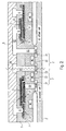
- FIG. 1 shows a stacked cell memory cell in the left part of the figure and in the right part of the figure an offset cell memory cell shown on a common semiconductor substrate 1.
- the jagged line in the middle of the figure indicates assume that the two different memory cells in the Usually not in practice on the same semiconductor substrate are arranged.
- a source region 23 common to both memory cells is provided on the semiconductor substrate 1. Furthermore, a drain region 21 is provided in each case. There is a gate 22 between the drain and source, so that a MOS transistor 2 is formed for each of the two memory cells, which serves as a selection transistor.
- the gate 22 is electrically connected to a word line WL.
- the word lines WL and the MOS transistors 2 are embedded in a first insulation layer 7, which consists for example of SiO 2 .
- the drain region 21 of the one shown in the left part of the figure Stacked cell memory cell is over a padded with tungsten Contact hole 64 with one over the first insulation layer 7 arranged first electrode 31 of a storage capacitor 3 connected.
- a second electrode 33 is applied so that the first and the second electrode 31, 33 with the intermediate one Dielectric 32 form the storage capacitor 3.
- the Offset Cell and however, the stacked cell differ in terms of Extension of the capacitor layers 31, 32, 33 along the Surface of the first insulation layer 7 and in terms the electrical contacting of the electrodes 31, 33.
- the electrode 31 is stacked cell, as already described, contacted from below.
- the offset cell is first electrode 31 in an area in which neither Dielectric 32 still the second electrode 33 over the first Extend electrode 31, contacted from above. This is a Contact hole 6 through an embedding the storage capacitor 3 second insulation layer 5 has been etched through and with Tungsten has been replenished.
- electrode 33 is from above, in each case through a contact hole 6 in the second insulation layer 5 therethrough.
- the offset cell (right part of the figure) is second electrode 33 continues via an electrical connection 62 extending along the surface of the second insulation layer 5 extends, and over a filled with tungsten Contact hole 61 through the first and second insulation layers 5, 7 through with the drain region 21 electrically connected.
- Another contact hole 65 extends outgoing from the source region 23 through the first and the second Insulation layer 5, 7 through to the surface of the second insulation layer 5 to a bit line BL.
- the offset cell including its electrical contacting and including the MOS transistor 2, thus takes up a much larger volume.
- the stacked cell places higher demands on precision and effort in its manufacture.
- a layer-like barrier 4 is applied to the second electrode 33, which is intended to protect the storage capacitor 3 against the ingress of hydrogen.
- the dielectrics 32 of the storage capacitors 3 consist of one of the hydrogen-sensitive materials already mentioned.
- the barrier 4 was structured so that in the areas of the later contact holes 61, 65 each has an opening with a width Z that is larger than the width of the contact hole 61, 65.
- Structuring barrier 4 became the second insulation layer 5 applied.
- the contact holes 6, 61, 65 etched and metallized.
- another Cover layer 8 on the surface of the second insulation layer 5 or applied to the metallization.
- Fig. 2 are also a memory cell of the stakked Cell type and offset cell type are shown.
- This two memory cells differ in terms of Structuring the barrier 4 from that shown in Fig. 1 Memory cells.
- the barrier 4 and the dielectric 32 structured together, especially using same or similar masks.
- the barrier 4 is not in Is in contact with the first electrode 31. Therefore, for the Barrier 4 also fully conductive materials be used. Should such materials also be used by Barrier 4 of the offset cell according to FIG. 1 are used, special measures are required, for example constructive Changes or there must be one applied first Partial layer of the barrier 4 made of electrically insulating material consist.
- FIGS. 1 and 2 Examples of a barrier against passage of hydrogen, as shown in FIGS. 1 and 2 Memory cells are present, are now based on of Fig. 3 and Fig. 4 explained in more detail.
- FIG. 3 shows a four-layer structure with a silicon dioxide layer 41, consisting of a lower partial layer 411 and an upper partial layer 412, and with a barrier layer 42, consisting of a lower partial layer 421 and an upper partial layer 422.
- the lower partial layer 411 of the silicon dioxide Layer 41 is, for example, applied directly to the second electrode 33 of the storage capacitors 3 shown in FIGS. 1 and 2, specifically as TEOS oxide in a PECVD (Plasma Enhanced Chemical Vapor Deposition) process, a plasma being ignited and so the reaction to SiO 2 is excited.
- PECVD Pullasma Enhanced Chemical Vapor Deposition
- the storage capacitor After the application of the first sub-layer 411, the storage capacitor together with the first partial layer 411 of an annealing, preferably at a temperature of 700 ° C, 30 minutes long in an oxygen atmosphere at atmospheric pressure.
- the tempering can also be carried out in shorter time and at different temperatures. Good results can be achieved especially when the temperature of the storage capacitor and the lower sub-layer 411 is 500 ° C for at least 5 minutes during the tempering.
- the upper partial layer 412 is deposited directly on the surface of the first partial layer 411 in an HTO (high temperature oxide) process with the starting gases SiH 4 and N 2 O at approx. 700 ° C. and a pressure of 40 Pa.
- HTO high temperature oxide
- the entire silicon dioxide layer 41 and the storage capacitor are then subjected to an annealing again, in particular under the same conditions as immediately after the application of the lower sub-layer 411.
- the lower partial layer 421 of the barrier layer 42 is applied directly to the upper partial layer 412 of the silicon dioxide layer 41.
- the deposition processes required for this are known per se and depend on the respective material of the lower partial layer 421. This can consist, for example, of ZrO x , TiN, Ti or AlO x .
- annealing can be carried out again.
- the upper partial layer 422 of the barrier layer 42 is applied directly to the lower partial layer 421.
- the material of the upper partial layer 422 is preferably Si 3 N 4 , which is deposited in an LPCVD (Low Pressure Chemical Vapor Deposition) process at approx. 750 ° C. and a pressure of 30 Pa or in a PECVD process.
- the Si 3 N 4 deposited in this process has an excellent barrier effect against the passage of hydrogen and itself contains practically no hydrogen.
- the hydrogen-containing gases SiH 2 Cl 2 (SiH 4 ) and NH 3 are used in the production of the Si 3 N 4 layer, the previous application of the lower partial layer 421 has an advantageous effect and protects the storage capacitor from irreversible damage.
- the lower sub-layer 421 can be produced in a hydrogen-free deposition process and in particular consist of one of the metal oxides which are generally difficult to etch. However, since the lower sub-layer 421 of the barrier layer 42 does not have to have the complete barrier effect of the entire barrier layer 42, the lower sub-layer 421 can have a relatively small layer thickness of, for example, approximately 20 nm, so that the layer can be etched with reasonable effort.
- the layer thicknesses of the other partial layers are, for example, approximately: 25 nm for the lower partial layer 411 of the silicon dioxide layer 41, 25 nm for the upper partial layer 412 of the silicon dioxide layer 41 and 25 nm for the upper partial layer 422 of the barrier layer 42.
- FIG. 4 Another exemplary embodiment of a barrier against the passage of hydrogen is shown in FIG. 4.
- the lower partial layer 411 and the upper partial layer 412 of the silicon dioxide layer 41 are in particular produced and annealed in the same way as the corresponding layers of the exemplary embodiment according to FIG. 3.
- the barrier layer 42 according to FIG. 4 consists of a material and is preferably made of applied in a continuous process. In order to develop a good barrier effect, a layer thickness of the barrier layer 42 of 50 to 100 nm is preferred. It is further preferred to choose an easily etchable material, in particular TiN, TaN or another nitride of transition metals. LPCVD-SiN, PECVD-SiN, HO x or ZrO x is also conceivable as a material for the barrier layer 42.
- the invention is not limited to that described with reference to the figures Embodiments limited. Rather can for example, the silicon oxide layer one in one continuous process step generated layer and / or the tempering of a plurality of partial layers only after the sub-layers have been applied. In each In this case, however, the tempering leads to an improvement in the properties a storage capacitor.
Landscapes
- Semiconductor Memories (AREA)
- Semiconductor Integrated Circuits (AREA)
Abstract
Description
- Fig. 1
- einen Querschnitt durch eine DRAM-Speicherzelle gemäß dem Stacked Cell-Aufbau und eine DRAM-Speicherzelle nach dem Offset Cell-Aufbau.
- Fig. 2
- einen Querschnitt durch zwei weitere derartige Speicherzellen,
- Fig. 3
- einen Querschnitt durch den Schichtaufbau einer Wasserstoffbarriere gemäß einer ersten Ausführungsform und
- Fig. 4
- einen Querschnitt durch eine Wasserstoffbarriere gemäß einer zweiten Ausführungsform.
Bei beiden Speicherzellentypen ist auf die zweite Elektrode 33 eine schichtartige Barriere 4 aufgebracht, die den Speicherkondensator 3 gegen ein Eindringen von Wasserstoff schützen soll. Insbesondere bestehen die Dielektrika 32 der Speicherkondensatoren 3 aus einem der bereits genannten wasserstoffempfindlichen Materialien.
Claims (18)
- Verfahren zur Herstellung eines mikroelektronischen Bauelements, bei welchemunda) an einem Substrat (1) ein Speicherkondensator (3) gebildet wird, enthaltendeine erste Elektrode (31),eine zweite Elektrode (32) undzwischen den Elektroden (31, 32) ein ferroelektrisches oder paraelektrisches Dielektrikum (33),dadurch gekennzeichnet, daßa) an dem Speicherkondensator (3) eine gegen ein Hindurchtreten von Wasserstoff schützende Barriere (4) gebildet wird,
bei der Barrierebildungzunächst eine Siliziumoxid-Schicht (41) erzeugt wird,der Speicherkondensator (3) und zumindest ein Teil der Siliziumoxid-Schicht (41) getempert werden undauf die getemperte Siliziumoxid-Schicht (41) eine Barriereschicht (42) aufgebracht wird, die gegen ein Hindurchtreten von Wasserstoff schützt. - Verfahren nach Anspruch 1,
dadurch gekennzeichnet, daß
zumindest ein Teil der Barriereschicht (42) in einem wasserstoffreien Abscheideprozeß aufgebracht wird. - Verfahren nach Anspruch 1 oder 2,
dadurch gekennzeichnet, daß
die Barriereschicht (42) aus einer Mehrzahl von Teilschichten (421, 422) gebildet wird, die jeweils gegen ein Hindurchtreten von Wasserstoff schützen. - Verfahren nach Anspruch 3,
dadurch gekennzeichnet, daß
eine erste Teilschicht (421) der Barriereschicht (42) aufgebracht wird und danach eine zweite Teilschicht (422) aus Siliziumnitrid aufgebracht wird. - Verfahren nach Anspruch 4,
dadurch gekennzeichnet, daß
die Siliziumnitrid-Schicht in einem LP (Low Pressure)-Mikrowellenprozeß abgeschieden wird, in dem zumindest ein Prekursor des Siliziumnitrids durch Mikrowellenstrahlung aktiviert wird. - Verfahren nach einem der Ansprüche 1 bis 5,
dadurch gekennzeichnet, daß
zumindest ein Teil der Barriereschicht (42) nach seinem Aufbringen getempert wird. - Verfahren nach einem der Ansprüche 1 bis 6,
dadurch gekennzeichnet, daß
die Siliziumoxid-Schicht (41) aus einer Mehrzahl von Teilschichten (411, 412) gebildet wird. - Verfahren nach Anspruch 7,
dadurch gekennzeichnet, daß
die erste Teilschicht (411) in einem Niedertemperatur-Prozeß, insbesondere einem PECVD (Plasma Enhanced Chemical Vapor Deposition)-Prozeß abgeschieden wird. - Verfahren nach Anspruch 7 oder 8,
dadurch gekennzeichnet, daß
eine folgende Teilschicht (412) in einem Hochtemperatur-Prozeß, insbesondere einem HTO (High Temperature Oxide)-Prozeß abgeschieden wird. - Verfahren nach einem Ansprüche 7 bis 9,
dadurch gekennzeichnet, daß
die Temperung des Speicherkondensators (3) nach dem Aufbringen einer Teilschicht (411, 412), insbesondere jeweils nach dem Aufbringen einer der Teilschichten (411, 412), der Siliziumoxid-Schicht (41) durchgeführt wird. - Verfahren nach einem der Ansprüche 1 bis 10,
dadurch gekennzeichnet, daß
die Temperung des Speicherkondensators (3) und der Siliziumoxid-Schicht (41) in sauerstoffhaltiger Atmosphäre bei Temperaturen von mindestens 500°C, vorzugsweise mindestens 650°C durchgeführt wird. - Mikroelektronisches Bauelement mit:unda) einem Substrat (1),b) einem auf dem Substrat (1) gebildeten Speicherkondensator (3), enthaltend:eine erste Elektrode (31),eine zweite Elektrode (32) undzwischen den Elektroden (31, 32) ein ferroelektrisches oder paraelektrisches Dielektrikum (33),dadurch gekennzeichnet, daßa) einer auf einer der Elektroden (31, 32) aufgebrachten Barriere (4), die den Speicherkondensator (3) gegen ein Hindurchtreten von Wasserstoff durch die Barriere (4) schützt,
die Barriere (4) aufweist:eine auf der Elektrode (31) aufgebrachte Siliziumoxid-Schicht (41), die in sauerstoffhaltiger Atmosphäre getempert wurde, undeine auf die Siliziumoxid-Schicht (41) aufgebrachte Barriereschicht (42), die den Speicherkondensator (3) gegen ein Hindurchtreten von Wasserstoff schützt. - Bauelement nach Anspruch 12,
dadurch gekennzeichnet, daß
der Speicherkondensator (3) und die Barriere (4) in eine auf die Barriere (4) aufgebrachte Isolationsschicht (5) eingebettet sind. - Bauelement nach Anspruch 13,
dadurch gekennzeichnet, daß
in die Isolationsschicht (5) ein mit Wolfram aufgefülltes Kontaktloch (6) eingebracht ist, so daß eine der Elektroden (31, 33) elektrisch kontaktiert ist. - Bauelement nach einem der Ansprüche 12 bis 14,
dadurch gekennzeichnet, daß
die Siliziumoxid-Schicht (41) zwei getemperte Teilschichten (411, 412) unterschiedlicher Oxidstruktur aufweist. - Bauelement nach einem der Ansprüche 12 bis 15,
dadurch gekennzeichnet, daß
die Barriereschicht (42) zwei Teilschichten (421, 422) aus unterschiedlichem Material aufweist. - Bauelement nach Anspruch 16,
dadurch gekennzeichnet, daß
die näher an der Siliziumoxid-Schicht (41) gelegene Teilschicht (421) aus einem metalloxidhaltigen Material besteht und eine Schichtdicke von 50 nm oder weniger, vorzugsweise ca. 20 nm, hat. - Bauelement nach Anspruch 16 oder 17,
dadurch gekennzeichnet, daß
die weiter von der Siliziumoxid-Schicht (41) gelegene Teilschicht (422) eine Siliziumnitrid-Schicht ist, vorzugsweise mit einer Schichtdicke von 20 bis 30 nm.
Applications Claiming Priority (2)
| Application Number | Priority Date | Filing Date | Title |
|---|---|---|---|
| DE10041685A DE10041685C2 (de) | 2000-08-24 | 2000-08-24 | Verfahren zur Herstellung eines mikroelektronischen Bauelements |
| DE10041685 | 2000-08-24 |
Publications (2)
| Publication Number | Publication Date |
|---|---|
| EP1182698A2 true EP1182698A2 (de) | 2002-02-27 |
| EP1182698A3 EP1182698A3 (de) | 2002-07-24 |
Family
ID=7653702
Family Applications (1)
| Application Number | Title | Priority Date | Filing Date |
|---|---|---|---|
| EP01118994A Ceased EP1182698A3 (de) | 2000-08-24 | 2001-08-06 | Barriereschicht für einen Speicherkondensator |
Country Status (7)
| Country | Link |
|---|---|
| US (1) | US6649468B2 (de) |
| EP (1) | EP1182698A3 (de) |
| JP (1) | JP3939516B2 (de) |
| KR (1) | KR100453793B1 (de) |
| CN (1) | CN1162900C (de) |
| DE (1) | DE10041685C2 (de) |
| TW (1) | TW508756B (de) |
Cited By (1)
| Publication number | Priority date | Publication date | Assignee | Title |
|---|---|---|---|---|
| JPWO2020095785A1 (ja) * | 2018-11-07 | 2021-10-14 | ソニーセミコンダクタソリューションズ株式会社 | 磁気抵抗素子及び半導体装置 |
Families Citing this family (11)
| Publication number | Priority date | Publication date | Assignee | Title |
|---|---|---|---|---|
| US7071506B2 (en) * | 2003-09-05 | 2006-07-04 | Infineon Technologies Ag | Device for inhibiting hydrogen damage in ferroelectric capacitor devices |
| JP2005229001A (ja) | 2004-02-16 | 2005-08-25 | Toshiba Corp | 半導体装置及び半導体装置の製造方法 |
| CN100431155C (zh) * | 2004-06-28 | 2008-11-05 | 富士通株式会社 | 半导体器件及其制造方法 |
| JP2007059705A (ja) * | 2005-08-25 | 2007-03-08 | Seiko Epson Corp | キャパシタおよびその製造方法、強誘電体メモリ装置の製造方法、アクチュエータの製造方法、並びに、液体噴射ヘッドの製造方法 |
| US7304339B2 (en) * | 2005-09-22 | 2007-12-04 | Agile Rf, Inc. | Passivation structure for ferroelectric thin-film devices |
| JP2007165350A (ja) | 2005-12-09 | 2007-06-28 | Fujitsu Ltd | 半導体装置の製造方法 |
| JP2009105429A (ja) * | 2008-12-27 | 2009-05-14 | Seiko Epson Corp | 半導体装置の製造方法及び半導体装置 |
| US20130264620A1 (en) * | 2012-04-06 | 2013-10-10 | Texas Instruments Incorporated | Integrated circuit having ferroelectric memory with dense via barrier |
| US10170299B2 (en) * | 2015-07-01 | 2019-01-01 | Applied Materials, Inc. | Method to reduce trap-induced capacitance in interconnect dielectric barrier stack |
| JP6300773B2 (ja) * | 2015-10-23 | 2018-03-28 | 三菱電機株式会社 | 半導体圧力センサ |
| US11990470B2 (en) * | 2021-09-24 | 2024-05-21 | International Business Machines Corporation | Ferroelectric and paraelectric stack capacitors |
Citations (1)
| Publication number | Priority date | Publication date | Assignee | Title |
|---|---|---|---|---|
| JPH118360A (ja) * | 1997-06-18 | 1999-01-12 | Nec Corp | 半導体装置の構造およびその製造方法 |
Family Cites Families (9)
| Publication number | Priority date | Publication date | Assignee | Title |
|---|---|---|---|---|
| US5407855A (en) * | 1993-06-07 | 1995-04-18 | Motorola, Inc. | Process for forming a semiconductor device having a reducing/oxidizing conductive material |
| DE69433244T2 (de) * | 1993-08-05 | 2004-07-29 | Matsushita Electric Industrial Co., Ltd., Kadoma | Herstellungsverfahren für Halbleiterbauelement mit Kondensator von hoher dielektrischer Konstante |
| JP3027941B2 (ja) * | 1996-05-14 | 2000-04-04 | 日本電気株式会社 | 誘電体容量素子を用いた記憶装置及び製造方法 |
| JP3098474B2 (ja) * | 1997-10-31 | 2000-10-16 | 日本電気株式会社 | 半導体装置の製造方法 |
| US6225156B1 (en) * | 1998-04-17 | 2001-05-01 | Symetrix Corporation | Ferroelectric integrated circuit having low sensitivity to hydrogen exposure and method for fabricating same |
| US6225656B1 (en) * | 1998-12-01 | 2001-05-01 | Symetrix Corporation | Ferroelectric integrated circuit with protective layer incorporating oxygen and method for fabricating same |
| DE19904379A1 (de) * | 1999-02-03 | 2000-08-17 | Siemens Ag | Mikroelektronische Struktur |
| US6066868A (en) * | 1999-03-31 | 2000-05-23 | Radiant Technologies, Inc. | Ferroelectric based memory devices utilizing hydrogen barriers and getters |
| KR100353808B1 (ko) * | 1999-12-28 | 2002-09-26 | 주식회사 하이닉스반도체 | 반도체 소자의 보호막 형성 방법 |
-
2000
- 2000-08-24 DE DE10041685A patent/DE10041685C2/de not_active Expired - Fee Related
-
2001
- 2001-08-06 EP EP01118994A patent/EP1182698A3/de not_active Ceased
- 2001-08-23 JP JP2001253003A patent/JP3939516B2/ja not_active Expired - Fee Related
- 2001-08-23 TW TW090120715A patent/TW508756B/zh not_active IP Right Cessation
- 2001-08-24 CN CNB011257946A patent/CN1162900C/zh not_active Expired - Fee Related
- 2001-08-24 KR KR10-2001-0051380A patent/KR100453793B1/ko not_active Expired - Fee Related
- 2001-08-24 US US09/939,249 patent/US6649468B2/en not_active Expired - Lifetime
Patent Citations (2)
| Publication number | Priority date | Publication date | Assignee | Title |
|---|---|---|---|---|
| JPH118360A (ja) * | 1997-06-18 | 1999-01-12 | Nec Corp | 半導体装置の構造およびその製造方法 |
| US6174766B1 (en) * | 1997-06-18 | 2001-01-16 | Nec Corporation | Semiconductor device and method of manufacturing the semiconductor device |
Cited By (2)
| Publication number | Priority date | Publication date | Assignee | Title |
|---|---|---|---|---|
| JPWO2020095785A1 (ja) * | 2018-11-07 | 2021-10-14 | ソニーセミコンダクタソリューションズ株式会社 | 磁気抵抗素子及び半導体装置 |
| US12339334B2 (en) | 2018-11-07 | 2025-06-24 | Sony Semiconductor Solutions Corporation | Magnetoresistive element and semiconductor device |
Also Published As
| Publication number | Publication date |
|---|---|
| JP3939516B2 (ja) | 2007-07-04 |
| US20020025592A1 (en) | 2002-02-28 |
| JP2002076296A (ja) | 2002-03-15 |
| KR100453793B1 (ko) | 2004-10-20 |
| CN1162900C (zh) | 2004-08-18 |
| DE10041685A1 (de) | 2002-03-21 |
| US6649468B2 (en) | 2003-11-18 |
| DE10041685C2 (de) | 2002-06-27 |
| KR20020012148A (ko) | 2002-02-15 |
| CN1340853A (zh) | 2002-03-20 |
| EP1182698A3 (de) | 2002-07-24 |
| TW508756B (en) | 2002-11-01 |
Similar Documents
| Publication | Publication Date | Title |
|---|---|---|
| DE10000005C1 (de) | Verfahren zur Herstellung eines ferroelektrischen Halbleiterspeichers | |
| DE10131716B4 (de) | Verfahren zur Herstellung eines Kondensators für eine Halbleiterspeichervorrichtung durch eine zweistufige Thermalbehandlung | |
| DE19926711B4 (de) | Verfahren zur Herstellung eines ferroelektrischen Speicherbauelements | |
| DE69413665T2 (de) | Passivierungsverfahren für eine ferroelektrische integrierte Schaltung, das harte keramische Materialien benutzt | |
| DE69736895T2 (de) | Verfahren zur herstellung eines halbleiterspeichers | |
| DE10227346A1 (de) | Ferroelektrische Speichervorrichtung, die eine ferroelektrische Planarisationsschicht verwendet, und Herstellungsverfahren | |
| DE10041685C2 (de) | Verfahren zur Herstellung eines mikroelektronischen Bauelements | |
| DE10100695A1 (de) | Halbleitervorrichtung | |
| DE10228528A1 (de) | Diffusionssperrfilm und dessen Herstellungsverfahren, Halbleiterspeicher und dessen Herstellungsverfahren | |
| DE19963500C2 (de) | Verfahren zum Herstellen einer strukturierten metalloxidhaltigen Schicht, insbesondere einer ferroelektrischen oder paraelektrischen Schicht | |
| DE10053171C2 (de) | Verfahren zum Herstellen einer ferroelektrischen oder paraelektrischen metalloxidhaltigen Schicht und eines Speicherbauelements daraus | |
| EP1111083B1 (de) | Verfahren zur Herstellung einer strukturierten Metallschicht | |
| EP0931333B1 (de) | Herstellverfahren für eine hoch-epsilon-dielektrische oder ferroelektrische schicht | |
| DE10121657B4 (de) | Mikroelektronische Struktur mit Wasserstoffbarrierenschicht | |
| EP1166345A1 (de) | Verfahren zur herstellung einer mikroelektronischen struktur | |
| DE10009762B4 (de) | Herstellungsverfahren für einen Speicherkondensator mit einem Dielektrikum auf der Basis von Strontium-Wismut-Tantalat | |
| EP1202332B1 (de) | Kontaktierungsstruktur für einen ferroelektrischen Speicherkondensator und Verfahren zu ihrer Herstellung | |
| DE10152636A1 (de) | Halbleiterspeichereinrichtung sowie Verfahren zu deren Herstellung | |
| DE19929307C1 (de) | Verfahren zur Herstellung einer strukturierten Schicht und dadurch hergestellte Elektrode | |
| DE19857039A1 (de) | Mikroelektronische Struktur | |
| WO1998015014A1 (de) | Kondensator mit einem elektrodenkern und einer dünnen edelmetallschicht als erster elektrode | |
| EP0986095A2 (de) | Schichtanordnung mit einer Materialschicht und einer im Bereich der Korngrenzen der Materialschicht angeordneten Diffusionsbarrierenschicht, und Verfahren zur Herstellung derselben | |
| EP1164631A2 (de) | Verfahren zur Erzeugung von Öffnungen in einer Schicht | |
| DE19811068C1 (de) | Kondensator in integrierter Schaltung sowie Verfahren zur Herstellung eines derartigen Kondensators | |
| WO1998014992A1 (de) | Verfahren zum herstellen einer halbleiteranordnung |
Legal Events
| Date | Code | Title | Description |
|---|---|---|---|
| PUAI | Public reference made under article 153(3) epc to a published international application that has entered the european phase |
Free format text: ORIGINAL CODE: 0009012 |
|
| AK | Designated contracting states |
Kind code of ref document: A2 Designated state(s): AT BE CH CY DE DK ES FI FR GB GR IE IT LI LU MC NL PT SE TR |
|
| AX | Request for extension of the european patent |
Free format text: AL;LT;LV;MK;RO;SI |
|
| PUAL | Search report despatched |
Free format text: ORIGINAL CODE: 0009013 |
|
| AK | Designated contracting states |
Kind code of ref document: A3 Designated state(s): AT BE CH CY DE DK ES FI FR GB GR IE IT LI LU MC NL PT SE TR |
|
| AX | Request for extension of the european patent |
Free format text: AL;LT;LV;MK;RO;SI |
|
| 17P | Request for examination filed |
Effective date: 20021118 |
|
| R17P | Request for examination filed (corrected) |
Effective date: 20021118 |
|
| AKX | Designation fees paid |
Designated state(s): DE FR GB IE IT |
|
| 17Q | First examination report despatched |
Effective date: 20031117 |
|
| STAA | Information on the status of an ep patent application or granted ep patent |
Free format text: STATUS: THE APPLICATION HAS BEEN REFUSED |
|
| 18R | Application refused |
Effective date: 20061019 |