EP1182276A2 - Verfahren zur Herstellung einer ferroelektrischen Festkörperschicht unter Verwendung eines Hilfsstoffes - Google Patents
Verfahren zur Herstellung einer ferroelektrischen Festkörperschicht unter Verwendung eines Hilfsstoffes Download PDFInfo
- Publication number
- EP1182276A2 EP1182276A2 EP01119519A EP01119519A EP1182276A2 EP 1182276 A2 EP1182276 A2 EP 1182276A2 EP 01119519 A EP01119519 A EP 01119519A EP 01119519 A EP01119519 A EP 01119519A EP 1182276 A2 EP1182276 A2 EP 1182276A2
- Authority
- EP
- European Patent Office
- Prior art keywords
- auxiliary
- solid layer
- substrate
- layer
- reactor
- Prior art date
- Legal status (The legal status is an assumption and is not a legal conclusion. Google has not performed a legal analysis and makes no representation as to the accuracy of the status listed.)
- Granted
Links
Images

Classifications
-
- H—ELECTRICITY
- H10—SEMICONDUCTOR DEVICES; ELECTRIC SOLID-STATE DEVICES NOT OTHERWISE PROVIDED FOR
- H10P—GENERIC PROCESSES OR APPARATUS FOR THE MANUFACTURE OR TREATMENT OF DEVICES COVERED BY CLASS H10
- H10P14/00—Formation of materials, e.g. in the shape of layers or pillars
- H10P14/60—Formation of materials, e.g. in the shape of layers or pillars of insulating materials
- H10P14/69—Inorganic materials
- H10P14/692—Inorganic materials composed of oxides, glassy oxides or oxide-based glasses
- H10P14/6938—Inorganic materials composed of oxides, glassy oxides or oxide-based glasses the material containing at least one metal element, e.g. metal oxides, metal oxynitrides or metal oxycarbides
- H10P14/69398—Inorganic materials composed of oxides, glassy oxides or oxide-based glasses the material containing at least one metal element, e.g. metal oxides, metal oxynitrides or metal oxycarbides the material having a perovskite structure, e.g. BaTiO3
-
- C—CHEMISTRY; METALLURGY
- C23—COATING METALLIC MATERIAL; COATING MATERIAL WITH METALLIC MATERIAL; CHEMICAL SURFACE TREATMENT; DIFFUSION TREATMENT OF METALLIC MATERIAL; COATING BY VACUUM EVAPORATION, BY SPUTTERING, BY ION IMPLANTATION OR BY CHEMICAL VAPOUR DEPOSITION, IN GENERAL; INHIBITING CORROSION OF METALLIC MATERIAL OR INCRUSTATION IN GENERAL
- C23C—COATING METALLIC MATERIAL; COATING MATERIAL WITH METALLIC MATERIAL; SURFACE TREATMENT OF METALLIC MATERIAL BY DIFFUSION INTO THE SURFACE, BY CHEMICAL CONVERSION OR SUBSTITUTION; COATING BY VACUUM EVAPORATION, BY SPUTTERING, BY ION IMPLANTATION OR BY CHEMICAL VAPOUR DEPOSITION, IN GENERAL
- C23C16/00—Chemical coating by decomposition of gaseous compounds, without leaving reaction products of surface material in the coating, i.e. chemical vapour deposition [CVD] processes
- C23C16/22—Chemical coating by decomposition of gaseous compounds, without leaving reaction products of surface material in the coating, i.e. chemical vapour deposition [CVD] processes characterised by the deposition of inorganic material, other than metallic material
- C23C16/30—Deposition of compounds, mixtures or solid solutions, e.g. borides, carbides, nitrides
- C23C16/40—Oxides
- C23C16/409—Oxides of the type ABO3 with A representing alkali, alkaline earth metal or lead and B representing a refractory metal, nickel, scandium or a lanthanide
-
- C—CHEMISTRY; METALLURGY
- C23—COATING METALLIC MATERIAL; COATING MATERIAL WITH METALLIC MATERIAL; CHEMICAL SURFACE TREATMENT; DIFFUSION TREATMENT OF METALLIC MATERIAL; COATING BY VACUUM EVAPORATION, BY SPUTTERING, BY ION IMPLANTATION OR BY CHEMICAL VAPOUR DEPOSITION, IN GENERAL; INHIBITING CORROSION OF METALLIC MATERIAL OR INCRUSTATION IN GENERAL
- C23C—COATING METALLIC MATERIAL; COATING MATERIAL WITH METALLIC MATERIAL; SURFACE TREATMENT OF METALLIC MATERIAL BY DIFFUSION INTO THE SURFACE, BY CHEMICAL CONVERSION OR SUBSTITUTION; COATING BY VACUUM EVAPORATION, BY SPUTTERING, BY ION IMPLANTATION OR BY CHEMICAL VAPOUR DEPOSITION, IN GENERAL
- C23C16/00—Chemical coating by decomposition of gaseous compounds, without leaving reaction products of surface material in the coating, i.e. chemical vapour deposition [CVD] processes
- C23C16/44—Chemical coating by decomposition of gaseous compounds, without leaving reaction products of surface material in the coating, i.e. chemical vapour deposition [CVD] processes characterised by the method of coating
- C23C16/455—Chemical coating by decomposition of gaseous compounds, without leaving reaction products of surface material in the coating, i.e. chemical vapour deposition [CVD] processes characterised by the method of coating characterised by the method used for introducing gases into reaction chamber or for modifying gas flows in reaction chamber
- C23C16/45593—Recirculation of reactive gases
-
- C—CHEMISTRY; METALLURGY
- C30—CRYSTAL GROWTH
- C30B—SINGLE-CRYSTAL GROWTH; UNIDIRECTIONAL SOLIDIFICATION OF EUTECTIC MATERIAL OR UNIDIRECTIONAL DEMIXING OF EUTECTOID MATERIAL; REFINING BY ZONE-MELTING OF MATERIAL; PRODUCTION OF A HOMOGENEOUS POLYCRYSTALLINE MATERIAL WITH DEFINED STRUCTURE; SINGLE CRYSTALS OR HOMOGENEOUS POLYCRYSTALLINE MATERIAL WITH DEFINED STRUCTURE; AFTER-TREATMENT OF SINGLE CRYSTALS OR A HOMOGENEOUS POLYCRYSTALLINE MATERIAL WITH DEFINED STRUCTURE; APPARATUS THEREFOR
- C30B25/00—Single-crystal growth by chemical reaction of reactive gases, e.g. chemical vapour-deposition growth
- C30B25/02—Epitaxial-layer growth
-
- C—CHEMISTRY; METALLURGY
- C30—CRYSTAL GROWTH
- C30B—SINGLE-CRYSTAL GROWTH; UNIDIRECTIONAL SOLIDIFICATION OF EUTECTIC MATERIAL OR UNIDIRECTIONAL DEMIXING OF EUTECTOID MATERIAL; REFINING BY ZONE-MELTING OF MATERIAL; PRODUCTION OF A HOMOGENEOUS POLYCRYSTALLINE MATERIAL WITH DEFINED STRUCTURE; SINGLE CRYSTALS OR HOMOGENEOUS POLYCRYSTALLINE MATERIAL WITH DEFINED STRUCTURE; AFTER-TREATMENT OF SINGLE CRYSTALS OR A HOMOGENEOUS POLYCRYSTALLINE MATERIAL WITH DEFINED STRUCTURE; APPARATUS THEREFOR
- C30B29/00—Single crystals or homogeneous polycrystalline material with defined structure characterised by the material or by their shape
- C30B29/10—Inorganic compounds or compositions
- C30B29/16—Oxides
- C30B29/22—Complex oxides
- C30B29/32—Titanates; Germanates; Molybdates; Tungstates
-
- H—ELECTRICITY
- H10—SEMICONDUCTOR DEVICES; ELECTRIC SOLID-STATE DEVICES NOT OTHERWISE PROVIDED FOR
- H10B—ELECTRONIC MEMORY DEVICES
- H10B53/00—Ferroelectric RAM [FeRAM] devices comprising ferroelectric memory capacitors
- H10B53/30—Ferroelectric RAM [FeRAM] devices comprising ferroelectric memory capacitors characterised by the memory core region
-
- H—ELECTRICITY
- H10—SEMICONDUCTOR DEVICES; ELECTRIC SOLID-STATE DEVICES NOT OTHERWISE PROVIDED FOR
- H10D—INORGANIC ELECTRIC SEMICONDUCTOR DEVICES
- H10D1/00—Resistors, capacitors or inductors
- H10D1/60—Capacitors
- H10D1/68—Capacitors having no potential barriers
- H10D1/682—Capacitors having no potential barriers having dielectrics comprising perovskite structures
-
- H—ELECTRICITY
- H10—SEMICONDUCTOR DEVICES; ELECTRIC SOLID-STATE DEVICES NOT OTHERWISE PROVIDED FOR
- H10P—GENERIC PROCESSES OR APPARATUS FOR THE MANUFACTURE OR TREATMENT OF DEVICES COVERED BY CLASS H10
- H10P14/00—Formation of materials, e.g. in the shape of layers or pillars
- H10P14/60—Formation of materials, e.g. in the shape of layers or pillars of insulating materials
- H10P14/63—Formation of materials, e.g. in the shape of layers or pillars of insulating materials characterised by the formation processes
- H10P14/6326—Deposition processes
- H10P14/6328—Deposition from the gas or vapour phase
- H10P14/6334—Deposition from the gas or vapour phase using decomposition or reaction of gaseous or vapour phase compounds, i.e. chemical vapour deposition
-
- H—ELECTRICITY
- H10—SEMICONDUCTOR DEVICES; ELECTRIC SOLID-STATE DEVICES NOT OTHERWISE PROVIDED FOR
- H10P—GENERIC PROCESSES OR APPARATUS FOR THE MANUFACTURE OR TREATMENT OF DEVICES COVERED BY CLASS H10
- H10P14/00—Formation of materials, e.g. in the shape of layers or pillars
- H10P14/60—Formation of materials, e.g. in the shape of layers or pillars of insulating materials
- H10P14/66—Formation of materials, e.g. in the shape of layers or pillars of insulating materials characterised by the type of materials
- H10P14/668—Formation of materials, e.g. in the shape of layers or pillars of insulating materials characterised by the type of materials the materials being characterised by the deposition precursor materials
Definitions
- the invention relates to a method for producing a ferroelectric or paraelectric solid layer by chemical vapor deposition (CVD) on a substrate according to the preamble of the claim 1.
- CVD chemical vapor deposition
- ferro- or for different purposes use paraelectric materials.
- Such layers can substitute for that normally from an oxide or Nitride layer existing dielectric of a storage capacitor of a DRAM semiconductor memory can be used.
- the One advantage of these so-called FeRAMs lies in the very much higher dielectric constant of the ferroelectric Material and on the other hand in the possibility of remanent Polarization of the ferroelectric material manufacture non-volatile memory device.
- a ferroelectric Layer alternatively for the gate oxide layer as an insulation layer between the gate electrode and the channel section of the semiconductor surface are formed, creating a non-volatile Memory transistor can be made.
- ferroelectric materials are the compositions known as strontium bismuth tantalate, SrBi 2 Ta 2 O 9 (SBT) and SrBi 2 (Ta, Nb) 2 O 9 (SBTN), and also Pb (Zr, Ti) O 3 (PZT) , Lead zirconate titanate) or Bi 4 Ti 3 O 12 (BTO) conceivable for practical use in a ferroelectric storage capacitor or a storage transistor.
- strontium bismuth tantalate SrBi 2 Ta 2 O 9 (SBT) and SrBi 2 (Ta, Nb) 2 O 9 (SBTN
- Pb (Zr, Ti) O 3 (PZT) Pb
- PZr, Ti) O 3 (PZT) Pb
- PZT Zinct-T
- PZT Lead zirconate titanate
- BTO Bi 4 Ti 3 O 12
- barium strontium titanate in the composition (Ba, Sr) TiO 3 (BST) is known as
- ferroelectric or paraelectric materials For the intended applications as a ferroelectric memory component in the highest packing density, it is necessary to deposit the ferroelectric or paraelectric materials with a sufficiently high deposition rate and very good uniformity of the layer thickness and stoichiometry over a large wafer.
- these requirements can be met with the deposition from the gas phase, ie a CVD process, in particular - with the participation of metals - an organometallic CVD (MOCVD) process.
- MOCVD organometallic CVD
- ferroelectric SBT these are, for example, Sr (thd) 2 , Bi (thd) 3 and Ta (ipro) 4 (thd), which are brought to deposition in an oxidizing atmosphere and thermally activated.
- the film In order to obtain the desired para- or ferroelectric material properties, it is necessary to deposit the film in the correct stoichiometry and in a suitable arrangement at the atomic level so that, for example, the Aurivillius phase with suitable stoichiometry, grain size and a preferred [100] - and [110] orientation.
- the organometallic compounds are used for the CVD process made gaseous in an evaporator and together with the Carrier gas argon and oxygen via a distributor plate (Perforated plate) passed into the reactor chamber.
- the precursors get to the wafer, which is at a higher temperature is heated to the activation energy necessary for the deposition to deliver.
- the reaction products and the radicals that are not decomposed will then flow in with the gas transported to the outside of the reactor from where it was pumped out become. At this point there are more reactions in the gas phase as well as on the inner walls of the reactor instead of.
- An essential idea of the present invention is in a process for making a crystalline, ferroelectric or paraelectric solid layer by vapor deposition (CVD) on a substrate in addition to the elements of the solid layer to be deposited containing starting gases at least one auxiliary initiate into the reaction space, which excipient is such that it contains molecules that have a dipole moment have and also have the property during the deposition process
- Substrate surface with perpendicular to the substrate surface Add dipole moment, so the crystal structure of the to specify the layer to be grown.
- the invention is based on simulation calculations and experiments gained knowledge that during the deposition process, as it was done in the past such polar molecules play an important role in growing up the shift with the correct pre-alignment the later play ferroelectric layer. It was found that polar molecules such as water or methanol as decomposition products the precursors in the different reactions arise and appear as adsorbate with their dipole moment Align perpendicular to the surface and thus the pre-alignment the later ferroelectric layer and thus its polarizability influence.
- reaction products are essentially completely drained and there is no significant Back diffusion and attachment to the surface. It
- the layer was spatial grows homogeneously and with a constant layer thickness, but none has ferroelectric properties.
- the polar molecules are obvious for the production of a layer with ferroelectric properties necessary.
- the present invention therefore draws from that Reaction chamber the gas mixture used from organometallic Precursors and carrier gas target molecules with dipole moment to be mixed in a low concentration, by which the desired orientation of the layer to be grown favors can be.
- the gas mixture used from organometallic Precursors and carrier gas target molecules with dipole moment to be mixed in a low concentration, by which the desired orientation of the layer to be grown favors can be.
- the polar molecules controlled from all sides to the Substrate surface and not - as before - only by diffusion from the outside of the reactor.
- about the amount of Auxiliary agent supplied is another control option for the process of the previous sizes such as composition in the gas phase, temperature and pressure.
- the invention is not limited to ferroelectric Layers with perovskite structure applicable, but generally on all solid layers where there is a certain Alignment and / or layer sequence of the crystal structure arrives.
- the meanwhile absorbed polar molecules act like a virtual scaffold that is constantly its shape changes because the polar molecules only each are temporarily absorbed to in their immediate vicinity for the correct alignment of the layer to be grown and then diffuse back into the gas phase.
- the auxiliary can, for example Be water or methanol; own in both cases the corresponding water or methanol molecules have a dipole moment.
- reaction products pumped out of the reaction chamber Deposition process of the reaction chamber again to others Place are fed.
- This second embodiment can generally be used in all cases where it is known that reaction products exist whose Molecules have a dipole moment.
- the process according to the invention is preferably carried out in a reactor chamber carried out in which a distributor plate, in particular a perforated plate is arranged, on one of which Side the starting gases for the deposition process, the auxiliary and optionally a carrier gas through inlet openings in the reactor wall are introduced, and on the other side of that Substrate is supported.
- a distributor plate in particular a perforated plate
- Side the starting gases for the deposition process, the auxiliary and optionally a carrier gas through inlet openings in the reactor wall are introduced, and on the other side of that Substrate is supported.
- a reactor wall opposite Outlet opening which is connected to a pump, with the the reaction products are pumped out of the reactor chamber.
- the inlet opening for the auxiliary with an external storage container connected while for the second embodiment of the invention this inlet port with a downstream of the substrate connected outlet openings in a reactor wall through which the reaction products are passed and thus again into the reactor chamber on one side of the Distribution plate are returned.
- the conditions of vapor deposition depend on the one used Reactor concept essentially from the distance of the distributor plate to the substrate. At a relatively large distance a situation arises as described at the beginning is, namely, by back diffusion or the like a certain density of reaction products above that Substrate wafer sets. In this case there is a Superimposition of the density of the supplied auxiliary and this Reaction products that lead to inhomogeneities in growth can lead. In a preferred mode of application of the invention is therefore carried out in such a way that there is no appreciable back diffusion of the reaction products comes so that molecules through which the growth of the Layer is influenced positively, essentially or for Can be supplied entirely by the supplied auxiliary. Thereby it is ensured that the density of such molecules is spatially constant above the substrate. This can be done can be achieved by a relatively small distance between Distribution plate and substrate wafer is set. The distance should be less than 2 cm, preferably about 1 cm.
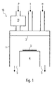
- a reactor chamber 10 shown in FIG. 1 is for example executed cylindrical and has a reactor wall 1 on the top of the cylindrical Reactor chamber has three inlet openings through the exit gases such as suitable precursors P, a carrier gas T and an auxiliary H of the reactor chamber 1 are supplied.
- the Precursor P is usually fed in and in liquid form converted into the gaseous state in an evaporator 11.
- a distributor plate 2 Is located at a distance below the inlet openings a distributor plate 2, usually a perforated plate, through which generates an approximately laterally homogeneous gas flow.
- a substrate wafer 3 mounted on a heatable susceptor 4 in a suitable manner.
- the precursors P Sr (thd) 2 , Bi (thd) 3 and Ta (ipro) 4 (thd) are used, for example.
- argon and oxygen can be used as carrier gas T.
- Water or methanol can be supplied as auxiliary H from an external storage container.
- FIG. 2 In the embodiment according to FIG. 2 is in the Reactor chamber 21 in addition to the gas outlet 25 another lateral opening 26 in the reactor wall 21 downstream of the substrate 23.
- This additional outlet opening 26 is through a pipe 27 with the inlet for the auxiliary H connected to the inlet chamber provided in the reactor chamber 20.
- the auxiliary H is pumped out by a part of the Reaction products formed.
- a valve 28 the gas flow in the pipeline 27 can be returned Reaction products are controlled.
- a ferroelectric Storage capacitor and a storage capacitor containing DRAM semiconductor memory can be produced.
- the surface of the substrate 3 or 23 is through the lower electrode layer of the storage capacitor is formed.
- a ferroelectric can also be used with the method according to the invention Memory transistor are manufactured, in which Fall the surface of the substrate 3 or 23 through the Channel section of a MOS transistor is formed.
Landscapes
- Chemical & Material Sciences (AREA)
- Metallurgy (AREA)
- Engineering & Computer Science (AREA)
- Materials Engineering (AREA)
- Organic Chemistry (AREA)
- Chemical Kinetics & Catalysis (AREA)
- General Chemical & Material Sciences (AREA)
- Mechanical Engineering (AREA)
- Inorganic Chemistry (AREA)
- Crystallography & Structural Chemistry (AREA)
- Chemical Vapour Deposition (AREA)
- Formation Of Insulating Films (AREA)
- Crystals, And After-Treatments Of Crystals (AREA)
Abstract
Description
- Fig. 1
- eine Querschnittsansicht einer Reaktorkammer gemäß einer ersten Ausführungsart der Erfindung;
- Fig. 2
- eine Querschnittsansicht einer Reaktorkammer gemäß einer zweiten Ausführungsart der Erfindung.
Claims (7)
- Verfahren zur Herstellung einer kristallinen Festkörperschicht durch Gasphasenabscheidung (CVD) auf einem Substrat (3; 23),
dadurch gekennzeichnet, daßzusätzlich zu den die Elemente der abzuscheidenden Festkörperschicht enthaltenden Ausgangsgasen (P) mindestens ein Hilfsstoff (H) in den Reaktionsraum eingeleitet wird,welcher Hilfsstoff (H) derart beschaffen ist, daß er Moleküle enthält, die ein Dipolmoment aufweisen und die Eigenschaft haben, sich während dem Abscheideprozeß kurzzeitig an der Substratoberfläche mit zu der Substratoberfläche senkrechten Dipolmoment anzulagern, um somit die Kristallstruktur der Festkörperschicht vorzugeben. - Verfahren nach Anspruch 1,
dadurch gekennzeichnet, daßder Hilfsstoff (H) aus einer externen Versorgungsquelle wie einem Vorratsbehälter zugeführt wird. - Verfahren nach Anspruch 1,
dadurch gekennzeichnet, daßder Hilfsstoff (H) im wesentlichen aus den aus dem Reaktionsraum (1; 21) abgepumpten Reaktionsprodukten der Gasphasenabscheidung besteht. - Verfahren nach einem der vorhergehenden Ansprüche,
dadurch gekennzeichnet, daßdie Festkörperschicht eine ferroelektrische oder paraelektrische Festkörperschicht ist, welche insbesondere eine Perowskit-Struktur aufweist. - Verfahren nach einem der vorhergehenden Ansprüche,
dadurch gekennzeichnet, daßder Reaktionsraum durch den Innenraum einer Reaktorkammer (1; 21) gebildet wird,in welcher eine Verteilerplatte (2; 22), insbesondere eine Lochplatte, angeordnet ist,auf deren einer Seite die Ausgangsgase (P), der Hilfsstoff (H) und ggf. ein Trägergas (T) durch Einlaßöffnungen in der Reaktorwand (1; 21) eingeleitet werden undauf deren anderer Seite das Substrat (3; 23) gehaltert ist, unddie Reaktorkammer ferner einen Gasauslaß (5; 25) aufweist, durch den die Reaktionsprodukte abgepumpt werden. - Verfahren nach Anspruch 5,
dadurch gekennzeichnet, daßdie Reaktorkammer (20) eine weitere Gasauslaßöffnung (26) in der Reaktorwand (21) stromabwärts des Substrats (23) aufweist, wobeidie Gasauslaßöffnung (26) mittels einer Verbindungsleitung (27) mit einer Einlaßöffnung stromabwärts der Verteilerplatte (2) verbunden ist. - Verfahren nach Anspruch 6,
dadurch gekennzeichnet, daßin der Verbindungsleitung (27) ein Ventil (28) zur Steuerung des Gasflusses angeordnet ist.
Applications Claiming Priority (2)
| Application Number | Priority Date | Filing Date | Title |
|---|---|---|---|
| DE10041698A DE10041698A1 (de) | 2000-08-24 | 2000-08-24 | Verfahren zur Herstellung einer ferroelektrischen Festkörperschicht unter Verwendung eines Hilfsstoffes |
| DE10041698 | 2000-08-24 |
Publications (3)
| Publication Number | Publication Date |
|---|---|
| EP1182276A2 true EP1182276A2 (de) | 2002-02-27 |
| EP1182276A3 EP1182276A3 (de) | 2003-12-03 |
| EP1182276B1 EP1182276B1 (de) | 2008-01-02 |
Family
ID=7653713
Family Applications (1)
| Application Number | Title | Priority Date | Filing Date |
|---|---|---|---|
| EP01119519A Expired - Lifetime EP1182276B1 (de) | 2000-08-24 | 2001-08-14 | Verfahren zur Herstellung einer ferroelektrischen Festkörperschicht unter Verwendung eines Hilfsstoffes |
Country Status (7)
| Country | Link |
|---|---|
| US (1) | US20020025377A1 (de) |
| EP (1) | EP1182276B1 (de) |
| JP (1) | JP2002118107A (de) |
| KR (1) | KR100453792B1 (de) |
| CN (1) | CN1344819A (de) |
| DE (2) | DE10041698A1 (de) |
| TW (1) | TW536813B (de) |
Family Cites Families (10)
| Publication number | Priority date | Publication date | Assignee | Title |
|---|---|---|---|---|
| US4468283A (en) * | 1982-12-17 | 1984-08-28 | Irfan Ahmed | Method for etching and controlled chemical vapor deposition |
| JPS6026663A (ja) * | 1983-07-25 | 1985-02-09 | Toshiba Ceramics Co Ltd | Cvd炉用水素排ガス回収装置 |
| US5185317A (en) * | 1988-02-19 | 1993-02-09 | Northwestern University | Method of forming superconducting Tl-Ba-Ca-Cu-O films |
| JPH03197394A (ja) * | 1989-12-25 | 1991-08-28 | Sumitomo Electric Ind Ltd | 有機結晶の成長方法 |
| JPH04137532A (ja) * | 1990-04-23 | 1992-05-12 | Toshiba Corp | 表面処理方法及びその装置 |
| US5104690A (en) * | 1990-06-06 | 1992-04-14 | Spire Corporation | CVD thin film compounds |
| US5753300A (en) * | 1995-06-19 | 1998-05-19 | Northwestern University | Oriented niobate ferroelectric thin films for electrical and optical devices and method of making such films |
| US6039834A (en) * | 1997-03-05 | 2000-03-21 | Applied Materials, Inc. | Apparatus and methods for upgraded substrate processing system with microwave plasma source |
| US6191054B1 (en) * | 1998-10-08 | 2001-02-20 | Matsushita Electric Industrial Co., Ltd. | Method for forming film and method for fabricating semiconductor device |
| US6477980B1 (en) * | 2000-01-20 | 2002-11-12 | Applied Materials, Inc. | Flexibly suspended gas distribution manifold for plasma chamber |
-
2000
- 2000-08-24 DE DE10041698A patent/DE10041698A1/de not_active Ceased
-
2001
- 2001-08-14 EP EP01119519A patent/EP1182276B1/de not_active Expired - Lifetime
- 2001-08-14 DE DE50113426T patent/DE50113426D1/de not_active Expired - Fee Related
- 2001-08-22 JP JP2001251144A patent/JP2002118107A/ja active Pending
- 2001-08-23 TW TW090120713A patent/TW536813B/zh not_active IP Right Cessation
- 2001-08-24 US US09/939,330 patent/US20020025377A1/en not_active Abandoned
- 2001-08-24 CN CN01125797A patent/CN1344819A/zh active Pending
- 2001-08-24 KR KR10-2001-0051379A patent/KR100453792B1/ko not_active Expired - Fee Related
Also Published As
| Publication number | Publication date |
|---|---|
| KR100453792B1 (ko) | 2004-10-20 |
| EP1182276B1 (de) | 2008-01-02 |
| KR20020016590A (ko) | 2002-03-04 |
| DE10041698A1 (de) | 2002-03-14 |
| EP1182276A3 (de) | 2003-12-03 |
| DE50113426D1 (de) | 2008-02-14 |
| JP2002118107A (ja) | 2002-04-19 |
| TW536813B (en) | 2003-06-11 |
| CN1344819A (zh) | 2002-04-17 |
| US20020025377A1 (en) | 2002-02-28 |
Similar Documents
| Publication | Publication Date | Title |
|---|---|---|
| DE10194692B4 (de) | Verfahren zur chemischen Aufdampfung zur Bildung einer dielektrischen Schicht mit hohem K-Wert und Verfahren zur Bildung eines Kondensators | |
| DE69702185T2 (de) | Anlage und vefahren zur beschichtung mittels eines nebelförmigen precursors mit verbessertem nebel und nebelführung | |
| DE69904910T2 (de) | Gaszuführsystem für cvd reaktor und verfahren zu dessen steuerung | |
| DE69804672T2 (de) | Verfahren zur selektiven ablagerung ferroelektrischer schichten auf wismut basis | |
| DE10132882B4 (de) | Verfahren zum Ausbilden einer Dünnschicht unter Verwendung einer Atomschichtabscheidung | |
| DE19534082A1 (de) | Verfahren zur Herstellung einer Halbleitereinrichtung | |
| DE10046021B4 (de) | Verfahren zur Herstellung von Kondensatoren auf Halbleitersubstraten in einer Einrichtung zur Bildung von Dünnfilmen | |
| DE60217610T2 (de) | Elektronische Anordnung mit einer Elektrode und ihre Herstellung | |
| DE69307533T2 (de) | Vorläufer und verfahren zur herstellung von metalloxiden | |
| DE19641058C2 (de) | Verfahren zur Bildung eines ferroelektrischen Dünnfilms und Vorrichtung dafür | |
| DE60035948T2 (de) | Chemischer abscheidungsreaktor und dessen verwendung für die abscheidung eines dünnen films | |
| DE69225388T2 (de) | Vorrichtung zur Bildung eines dünnen Films und Verfahren zur Bildung eines dünnen Films mittels dieser Vorrichtung | |
| DE19738330C2 (de) | Chemische Dampfabscheidungsvorrichtung, Abscheidungsverfahren für Metallorganische Verbindungen und Verwendung des Verfahrens | |
| DE69115172T2 (de) | Verfahren zum Herstellen eines kapazitiven isolierenden Films. | |
| DE10137088A1 (de) | Verfahren zum Ausbilden von siliziumhaltigen Dünnschichten mittels Atomschichtabscheidung (Atomic Layer Deposition) unter Verwendung von Trisdimethylaminosilan | |
| DE19851824C2 (de) | CVD-Reaktor | |
| DE69331743T2 (de) | Herstellungsverfahren von geschichteten uebergittermaterialien und von diesen enthaltenden elektronischen vorrichtungen | |
| DE10081315C2 (de) | Tetrahydrofuran-addierte Gruppe II-ß-Diketonat-Komplexe als Ausgangsreagenzien für chemisches Aufdampfen | |
| EP1733073B1 (de) | Verfahren zum abscheiden von insbesondere metalloxiden mittels nicht kontinuierlicher precursorinjektion | |
| DE69920967T2 (de) | Verfahren zur cvd unter verwendung von bi-alkoxiden | |
| DE10032213B4 (de) | Verfahren zur Herstellung eines Kondensators für ein Halbleiterspeicherbauelement | |
| DE10065224A1 (de) | Verfahren zur Herstellung von Kondensatoren für Halbleitereinrichtungen | |
| DE60035557T2 (de) | Verfahren und vorrichtung zur herstellung dünner filme | |
| DE10228798A1 (de) | Bilden ferroelektrischer Pb(Zr,Ti)O3-Filme | |
| DE60132950T2 (de) | Vakuumbehandlungsvorrichtung |
Legal Events
| Date | Code | Title | Description |
|---|---|---|---|
| PUAI | Public reference made under article 153(3) epc to a published international application that has entered the european phase |
Free format text: ORIGINAL CODE: 0009012 |
|
| AK | Designated contracting states |
Kind code of ref document: A2 Designated state(s): AT BE CH CY DE DK ES FI FR GB GR IE IT LI LU MC NL PT SE TR |
|
| AX | Request for extension of the european patent |
Free format text: AL;LT;LV;MK;RO;SI |
|
| PUAL | Search report despatched |
Free format text: ORIGINAL CODE: 0009013 |
|
| AK | Designated contracting states |
Kind code of ref document: A3 Designated state(s): AT BE CH CY DE DK ES FI FR GB GR IE IT LI LU MC NL PT SE TR |
|
| AX | Request for extension of the european patent |
Extension state: AL LT LV MK RO SI |
|
| 17P | Request for examination filed |
Effective date: 20040119 |
|
| AKX | Designation fees paid |
Designated state(s): DE FR GB IE IT |
|
| GRAP | Despatch of communication of intention to grant a patent |
Free format text: ORIGINAL CODE: EPIDOSNIGR1 |
|
| GRAS | Grant fee paid |
Free format text: ORIGINAL CODE: EPIDOSNIGR3 |
|
| GRAA | (expected) grant |
Free format text: ORIGINAL CODE: 0009210 |
|
| RAP1 | Party data changed (applicant data changed or rights of an application transferred) |
Owner name: QIMONDA AG |
|
| AK | Designated contracting states |
Kind code of ref document: B1 Designated state(s): DE FR GB IE IT |
|
| REG | Reference to a national code |
Ref country code: GB Ref legal event code: FG4D Free format text: NOT ENGLISH |
|
| REG | Reference to a national code |
Ref country code: IE Ref legal event code: FG4D Free format text: LANGUAGE OF EP DOCUMENT: GERMAN |
|
| REF | Corresponds to: |
Ref document number: 50113426 Country of ref document: DE Date of ref document: 20080214 Kind code of ref document: P |
|
| GBV | Gb: ep patent (uk) treated as always having been void in accordance with gb section 77(7)/1977 [no translation filed] | ||
| ET | Fr: translation filed | ||
| REG | Reference to a national code |
Ref country code: IE Ref legal event code: FD4D |
|
| PG25 | Lapsed in a contracting state [announced via postgrant information from national office to epo] |
Ref country code: IE Free format text: LAPSE BECAUSE OF FAILURE TO SUBMIT A TRANSLATION OF THE DESCRIPTION OR TO PAY THE FEE WITHIN THE PRESCRIBED TIME-LIMIT Effective date: 20080102 |
|
| PLBE | No opposition filed within time limit |
Free format text: ORIGINAL CODE: 0009261 |
|
| STAA | Information on the status of an ep patent application or granted ep patent |
Free format text: STATUS: NO OPPOSITION FILED WITHIN TIME LIMIT |
|
| 26N | No opposition filed |
Effective date: 20081003 |
|
| PG25 | Lapsed in a contracting state [announced via postgrant information from national office to epo] |
Ref country code: GB Free format text: LAPSE BECAUSE OF FAILURE TO SUBMIT A TRANSLATION OF THE DESCRIPTION OR TO PAY THE FEE WITHIN THE PRESCRIBED TIME-LIMIT Effective date: 20080102 |
|
| PGFP | Annual fee paid to national office [announced via postgrant information from national office to epo] |
Ref country code: DE Payment date: 20081010 Year of fee payment: 8 |
|
| REG | Reference to a national code |
Ref country code: FR Ref legal event code: ST Effective date: 20090430 |
|
| PG25 | Lapsed in a contracting state [announced via postgrant information from national office to epo] |
Ref country code: IT Free format text: LAPSE BECAUSE OF FAILURE TO SUBMIT A TRANSLATION OF THE DESCRIPTION OR TO PAY THE FEE WITHIN THE PRESCRIBED TIME-LIMIT Effective date: 20080102 Ref country code: FR Free format text: LAPSE BECAUSE OF NON-PAYMENT OF DUE FEES Effective date: 20080901 |
|
| PG25 | Lapsed in a contracting state [announced via postgrant information from national office to epo] |
Ref country code: DE Free format text: LAPSE BECAUSE OF NON-PAYMENT OF DUE FEES Effective date: 20100302 |