EP1180795A2 - Verfahren zum Herstellen einer ersten Elektrode und einer zweiten Elektrode, elektronisches Bauelement und elektronisches Speicherelement - Google Patents
Verfahren zum Herstellen einer ersten Elektrode und einer zweiten Elektrode, elektronisches Bauelement und elektronisches Speicherelement Download PDFInfo
- Publication number
- EP1180795A2 EP1180795A2 EP01118283A EP01118283A EP1180795A2 EP 1180795 A2 EP1180795 A2 EP 1180795A2 EP 01118283 A EP01118283 A EP 01118283A EP 01118283 A EP01118283 A EP 01118283A EP 1180795 A2 EP1180795 A2 EP 1180795A2
- Authority
- EP
- European Patent Office
- Prior art keywords
- electrode
- cluster
- clusters
- ion
- electronic
- Prior art date
- Legal status (The legal status is an assumption and is not a legal conclusion. Google has not performed a legal analysis and makes no representation as to the accuracy of the status listed.)
- Granted
Links
Images
Classifications
-
- C—CHEMISTRY; METALLURGY
- C23—COATING METALLIC MATERIAL; COATING MATERIAL WITH METALLIC MATERIAL; CHEMICAL SURFACE TREATMENT; DIFFUSION TREATMENT OF METALLIC MATERIAL; COATING BY VACUUM EVAPORATION, BY SPUTTERING, BY ION IMPLANTATION OR BY CHEMICAL VAPOUR DEPOSITION, IN GENERAL; INHIBITING CORROSION OF METALLIC MATERIAL OR INCRUSTATION IN GENERAL
- C23C—COATING METALLIC MATERIAL; COATING MATERIAL WITH METALLIC MATERIAL; SURFACE TREATMENT OF METALLIC MATERIAL BY DIFFUSION INTO THE SURFACE, BY CHEMICAL CONVERSION OR SUBSTITUTION; COATING BY VACUUM EVAPORATION, BY SPUTTERING, BY ION IMPLANTATION OR BY CHEMICAL VAPOUR DEPOSITION, IN GENERAL
- C23C14/00—Coating by vacuum evaporation, by sputtering or by ion implantation of the coating forming material
- C23C14/22—Coating by vacuum evaporation, by sputtering or by ion implantation of the coating forming material characterised by the process of coating
- C23C14/228—Gas flow assisted PVD deposition
-
- H—ELECTRICITY
- H10—SEMICONDUCTOR DEVICES; ELECTRIC SOLID-STATE DEVICES NOT OTHERWISE PROVIDED FOR
- H10D—INORGANIC ELECTRIC SEMICONDUCTOR DEVICES
- H10D84/00—Integrated devices formed in or on semiconductor substrates that comprise only semiconducting layers, e.g. on Si wafers or on GaAs-on-Si wafers
-
- C—CHEMISTRY; METALLURGY
- C23—COATING METALLIC MATERIAL; COATING MATERIAL WITH METALLIC MATERIAL; CHEMICAL SURFACE TREATMENT; DIFFUSION TREATMENT OF METALLIC MATERIAL; COATING BY VACUUM EVAPORATION, BY SPUTTERING, BY ION IMPLANTATION OR BY CHEMICAL VAPOUR DEPOSITION, IN GENERAL; INHIBITING CORROSION OF METALLIC MATERIAL OR INCRUSTATION IN GENERAL
- C23C—COATING METALLIC MATERIAL; COATING MATERIAL WITH METALLIC MATERIAL; SURFACE TREATMENT OF METALLIC MATERIAL BY DIFFUSION INTO THE SURFACE, BY CHEMICAL CONVERSION OR SUBSTITUTION; COATING BY VACUUM EVAPORATION, BY SPUTTERING, BY ION IMPLANTATION OR BY CHEMICAL VAPOUR DEPOSITION, IN GENERAL
- C23C14/00—Coating by vacuum evaporation, by sputtering or by ion implantation of the coating forming material
- C23C14/22—Coating by vacuum evaporation, by sputtering or by ion implantation of the coating forming material characterised by the process of coating
- C23C14/221—Ion beam deposition
-
- H—ELECTRICITY
- H10—SEMICONDUCTOR DEVICES; ELECTRIC SOLID-STATE DEVICES NOT OTHERWISE PROVIDED FOR
- H10D—INORGANIC ELECTRIC SEMICONDUCTOR DEVICES
- H10D1/00—Resistors, capacitors or inductors
- H10D1/60—Capacitors
- H10D1/68—Capacitors having no potential barriers
- H10D1/692—Electrodes
- H10D1/711—Electrodes having non-planar surfaces, e.g. formed by texturisation
- H10D1/712—Electrodes having non-planar surfaces, e.g. formed by texturisation being rough surfaces, e.g. using hemispherical grains
-
- H—ELECTRICITY
- H01—ELECTRIC ELEMENTS
- H01J—ELECTRIC DISCHARGE TUBES OR DISCHARGE LAMPS
- H01J2237/00—Discharge tubes exposing object to beam, e.g. for analysis treatment, etching, imaging
- H01J2237/06—Sources
- H01J2237/08—Ion sources
- H01J2237/0812—Ionized cluster beam [ICB] sources
-
- H—ELECTRICITY
- H01—ELECTRIC ELEMENTS
- H01J—ELECTRIC DISCHARGE TUBES OR DISCHARGE LAMPS
- H01J2237/00—Discharge tubes exposing object to beam, e.g. for analysis treatment, etching, imaging
- H01J2237/30—Electron or ion beam tubes for processing objects
- H01J2237/31—Processing objects on a macro-scale
- H01J2237/3142—Ion plating
- H01J2237/3146—Ion beam bombardment sputtering
-
- H—ELECTRICITY
- H10—SEMICONDUCTOR DEVICES; ELECTRIC SOLID-STATE DEVICES NOT OTHERWISE PROVIDED FOR
- H10D—INORGANIC ELECTRIC SEMICONDUCTOR DEVICES
- H10D64/00—Electrodes of devices having potential barriers
- H10D64/01—Manufacture or treatment
- H10D64/011—Manufacture or treatment of electrodes ohmically coupled to a semiconductor
- H10D64/0111—Manufacture or treatment of electrodes ohmically coupled to a semiconductor to Group IV semiconductors
- H10D64/0113—Manufacture or treatment of electrodes ohmically coupled to a semiconductor to Group IV semiconductors the conductive layers comprising highly doped semiconductor materials, e.g. polysilicon layers or amorphous silicon layers
-
- Y—GENERAL TAGGING OF NEW TECHNOLOGICAL DEVELOPMENTS; GENERAL TAGGING OF CROSS-SECTIONAL TECHNOLOGIES SPANNING OVER SEVERAL SECTIONS OF THE IPC; TECHNICAL SUBJECTS COVERED BY FORMER USPC CROSS-REFERENCE ART COLLECTIONS [XRACs] AND DIGESTS
- Y10—TECHNICAL SUBJECTS COVERED BY FORMER USPC
- Y10S—TECHNICAL SUBJECTS COVERED BY FORMER USPC CROSS-REFERENCE ART COLLECTIONS [XRACs] AND DIGESTS
- Y10S977/00—Nanotechnology
- Y10S977/70—Nanostructure
- Y10S977/773—Nanoparticle, i.e. structure having three dimensions of 100 nm or less
Definitions
- the invention relates to a method for producing a first electrode and a second electrode electronic component and an electronic Memory element.
- Electrodes for example of Silicon electrodes or metal electrodes too enlarge, so as large as possible electrical To reach the capacity of the electrodes.
- the electrodes are enlarged in the lateral direction due to the associated increase in space requirements such an electrode and the associated Enlargement of an electronic component with a Many such electrodes, often out of the question.
- Electrodes developed with trenches in a substrate are formed, generally electrode arrangements in three-dimensional structures in which the storage of the electrical charge carriers in a stacked Electrode arrangement or by using the vertical electrodes arranged in the trenches.
- Houghening an electrode surface it is known to provide additional, for example by means of a special etching process to increase the porosity of the surface or by applying spherical polysilicon structures on the surface of the electrodes, which is also referred to as H emispherical S ilicon G raines (HSG).
- HSG H emispherical S ilicon G raines
- polysilicon i.e. polycrystalline silicon
- Hemispherical are formed on the electrode surface Islands with a diameter of usually approximately 30 nm.
- a cluster ion source is also known from [1], by means of the nickel cluster is applied to a substrate surface become.
- [5] describes a method in which a Polysilicon electrode Argon or phosphorus cluster be applied.
- the invention is therefore based on the problem of a method for producing a first electrode and a second Electrode and an electronic formed with it Specify component and an electronic storage element, with a more precise adjustment of the grain size on the Isles formed surface is enabled.
- the problem is caused by the method of making one first electrode and a second electrode, the electronic component as well as the electronic Storage element with the features according to the independent Claims resolved.
- the first electrode and the second electrode made of an electrode material provided, for example, is integrated in a substrate, preferably in a silicon substrate.
- clusters from the Electrode material on the first electrode and / or second Electrode applied.
- the electrode material can be polycrystalline silicon, i.e. Polysilicon, as well as basically any free selectable metal such as nickel or silver.
- the invention makes it possible for the first time to be precisely specifiable generate a beam profile so that at the location of the Deposition, i.e. on the electrode surface of a an electrode to be roughened, if desired optimized, distribution of the clusters to be formed guaranteed becomes.
- the size of the clusters to be formed is very precise adjustable.
- Another advantage of the invention is that in a simple way and therefore inexpensive a very accurate Structuring the clusters on an electrode surface is made possible.
- the Electrode material can also be doped silicon, i.e. it are using silicon clusters on one accordingly desired doping atoms doped silicon electrodes formed, the doping atoms in a condensation region the cluster ion source that of the cluster ion source formed ion beam with generated silicon ions can be added, whereby the electrode material which is formed as a cluster on the electrode surface, has doped silicon clusters.
- any of the electrodes can be used electronic component are formed, which on this Contains electrodes formed in this way.
- a preferred area of use of an electrode formed in such a manner are electronic memory, such as an electronic memory element as a dynamic memory element with random access, ie, an R Andom A ccess M emory (RAM) or a flash EEPROM.
- electronic memory such as an electronic memory element as a dynamic memory element with random access, ie, an R Andom A ccess M emory (RAM) or a flash EEPROM.
- Another advantage of the invention is that almost (semi-) spherical ion clusters are formed can, so potentially another one this way Surface enlargement of the electrode surface achieved can be.
- grain sizes of the clusters are due to the invention can be generated, which are significantly smaller than that according to the known process producible grain sizes of the clusters, so that also the areas adjacent to closer spaces the electrode surface for a surface enlargement of the Electrode surface can be considered.
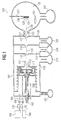
- FIG. 1 shows a cluster ion source 100 according to a first exemplary embodiment of the invention.
- the cluster ion source 100 basically has the same Structure based on the cluster ion source described in [1].
- Cooling circuit 102 provided with the coolant, according to this embodiment is filled with cooling water.
- a main chamber 103 is provided in the housing 101 Via a first feed line 104 argon in gas phase from a first gas container 105, which is filled with argon is called a continuous gas flow, which is by means of a first Mass flow controller 106 is regulated.
- the main chamber 103 becomes a second one Supply line 108 a doping gas, according to this Embodiment with boron atoms from a second Gas container 109, which is filled with the doping gas, supplied as a continuous or discrete gas stream, the is regulated by means of a second mass flow controller 110.
- the argon atoms are sputtered onto a target 111 Silicon shot and through a condensation area 112 the cluster ion source 100 is supplied with the Doping gas, so that starting from the sputtering target 111 Ion beam 113 is generated, which contains both the silicon ions and also contains the ions of the doping gas.
- the ion beam passes through a main chamber opening 114 a diameter of about 5 mm, whereby the Ion beam 113 is shaped in a predetermined manner.
- Another adjustment of the beam profile of the formed Ion beam 113 takes place through further openings 115, 116, 117 in further electrodes, their opening diameters in each case is about 5 mm and the different choice of electrical potentials applied to the electrodes become.
- the free argon atoms are through the first feed line 104 shot at the sputtering target 111 and through the Firing at the sputtering target 109 (silicon sputtering target) so-called fast silicon ions are generated.
- the ion clusters typically arise in different sizes from just a few to several thousand atoms, making their diameter smaller can be kept as the known diameter of Usually produced silicon islands, which according to the Known etching processes can be generated.
- the ion clusters are made by means of the diaphragms that the Define openings 112, 113, 114, 115, to a sharp limited ion beam 121 is formed, accelerated or else delayed and focused.
- the desired beam profile of the ion beam 113 is basically through the appropriate arrangement of the individual Apertures and the choice of electrical potentials on them Apertures freely adjustable.
- the sharply delimited ion beam 121 which is still a large one Number of ion clusters of different sizes and thus contains different masses, is characterized by a Mass separator 122, i.e. a device for Mass separation, performed as described in [3].
- the respective pressure in the secondary chambers 118, 119, 120 is guaranteed by additional turbomolecular pumps 123, 124, 125 each to the secondary chambers 118, 119, 120 are connected.
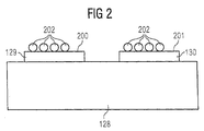
- the ion clusters are placed on a holder 127 attached substrate 128 on a first electrode 129 as well a second electrode 130, both on the substrate 128 are prefabricated, applied.
- the electrode surface 200 of the first electrode 129 or the electrode surface 201 of the second electrode 130 is roughened in a very easily adjustable manner by the ion clusters 202, so that an enlarged electrode surface 200 of the first electrode 129 and / or an enlarged electrode surface 201 of the second electrode 130 can be generated.
- the ion clusters 202 which are to be deposited on the first electrode 129 and / or the second electrode 130, are hit by an electric field directed in the opposite direction before striking the respective electrode surface 200, 201 , symbolized in Figure 1 by an arrow 131, braked.
- a further turbomolecular pump 132 is also provided, with the deposition chamber 133 in which the holder 127 is attached, coupled.
- the required size of the applied electric field depends on the desired energy of the ion cluster shortly before it hits the electrode surface 200, 201 and can be determined experimentally.
- the structuring of the electrode surfaces 200, 201 is suitable both for planar electrodes, as shown in FIG . 2 , and for electrodes which are arranged in three-dimensional structures, for example in trenches of predeterminable depth.
- ion clusters 202 on planar Electrode surfaces 200, 201 is a beam formation of the Ion beam with the broadest possible beam profile on site deposition, i.e. of hitting the Electrode surface 200, 201 is desirable.
- Cluster ion beam desirable either aimed at the location of the respective trench where the Ion cluster 202 is to be deposited in each case or via the entire electrode surface 200, 201 can be rasterized.
- the corresponding variability of the beam profile of the Ion beam can be selected by suitable choice of ion optical Lenses provided in the beam path of the ion beam and the voltages applied to the ion-optical lenses can be achieved.
- 201 can basically in further procedural steps, any electronic components, preferably DRAM memory elements and flash EEPROM memory elements getting produced.
- the device for mass separation 122 is suitable in accordance with an alternative embodiment of the invention so-called Vienna filter.
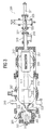
- a second cluster ion source 300 according to a second exemplary embodiment of the invention is shown in FIG .
- Helium gas is fed into a by means of a feed line 303 a main chamber 302 provided with a cooling element 301 above of a crucible 304, the silicon in the gas phase contains.
- the silicon gas in the crucible 104 is replaced by the Helium cooled and condensed to form clusters Main opening 305 are performed.
- the clusters are led into an area 306 which is kept at a pressure of approximately 10 -4 mbar by means of a diffusion pump 307.
- the cluster beam formed is doped with, according to this embodiment with boron atoms, doped with a cathode plasma generator 308.
- the doped cluster ion beam 309 is through a Beak opening 310 for focusing the cluster ion beam 309 led into a high vacuum area 311, which is connected to a another diffusion pump 312 is connected.
- the doped cluster ion beam 309 is in the high vacuum region 311 accelerated and further focused in one Acceleration area 313 and aligned in an X-Y deflector 314th
- a lens 315 focuses the doped cluster ion beam 309 further, and the doped focused in this way Cluster ion beam is used as a Wien filter 316 Mass selector supplied.
- a valve 322 is also between the drift tube 319 and the deposition chamber 323 is provided for controlling the from the Wien filter 316 and the drift tube 319 emerging cluster ion beam.
Landscapes
- Chemical & Material Sciences (AREA)
- Organic Chemistry (AREA)
- Engineering & Computer Science (AREA)
- Materials Engineering (AREA)
- Mechanical Engineering (AREA)
- Metallurgy (AREA)
- Chemical Kinetics & Catalysis (AREA)
- Physical Vapour Deposition (AREA)
- Non-Volatile Memory (AREA)
- Semiconductor Memories (AREA)
- Physical Deposition Of Substances That Are Components Of Semiconductor Devices (AREA)
- Electrodes Of Semiconductors (AREA)
- Electron Sources, Ion Sources (AREA)
Abstract
Description
- Figur 1
- eine Cluster-Ionenquelle zum Erzeugen einer Elektrodenanordnung mit aufgerauhter Elektrodenoberfläche gemäß einem ersten Ausführungsbeispiel der Erfindung;
- Figur 2
- einen Querschnitt durch ein elektronisches Bauelement mit zwei Elektroden mit aufgerauhter Elektrodenoberfläche gemäß einem Ausführungsbeispiel der Erfindung; und
- Figur 3
- eine Cluster-Ionenquelle gemäß einem zweiten Ausführungsbeispiel der Erfindung zum Erzeugen einer Elektrodenanordnung mit aufgerauhter Elektrodenoberfläche.
- ein zwischen der Hauptkammer 103 und der durch die erste Öffnung 115 gebildeter Bereich als eine erste Nebenkammer 118,
- eine zwischen der ersten Öffnung 115 und der zweiten Öffnung 116 gebildete zweite Nebenkammer 119, sowie
- eine dritte Nebenkammer 120 zwischen der zweiten Öffnung 116 und der dritten Öffnung 117.
- Phosphoratome,
- Boratome,
- Arsenatome, aber auch
- 100
- Cluster-Ionenquelle
- 101
- Gehäuse Cluster-Ionenquelle
- 102
- Kühlwasser-Anordnung
- 103
- Hauptkammer
- 104
- Erste Zuführleitung
- 105
- Erster Gasbehälter
- 106
- Erster Massenfluss-Regler
- 107
- Turbomolekulare Pumpe
- 108
- Zweite Zuführleitung
- 109
- Zweiter Gasbehälter
- 110
- Zweiter Massenfluss-Regler
- 111
- Sputter-Target
- 112
- Kondensationsbereich
- 113
- Cluster-Ionenstrahl
- 114
- Hauptkammer-Öffnung
- 115
- Erste Öffnung
- 116
- Zweite Öffnung
- 117
- Dritte Öffnung
- 118
- Erste Nebenkammer
- 119
- Zweite Nebenkammer
- 120
- Dritte Nebenkammer
- 121
- Scharf begrenzter Ionenstrahl
- 122
- Massenseparator
- 123
- Turbomolekulare Pumpe
- 124
- Turbomolekulare Pumpe
- 125
- Turbomolekulare Pumpe
- 126
- Ergebnis-Ionenstrahl
- 127
- Halterung
- 128
- Substrat
- 129
- Erste Elektrode
- 130
- Zweite Elektrode
- 131
- Pfeil
- 132
- Turbomolekulare Pumpe
- 200
- Elektrodenoberfläche erste Elektrode
- 201
- Elektrodenoberfläche zweite Elektrode
- 202
- Ionen-Cluster
- 300
- Cluster-Ionenquelle
- 301
- Kühlelement
- 302
- Hauptkammer
- 303
- Zuführleitung
- 304
- Tiegel
- 305
- Hauptöffnung
- 306
- Bereich
- 307
- Diffusionspumpe
- 308
- Kathodenplasma-Erzeuger
- 309
- Dotierter Cluster-Ionenstrahl
- 310
- Schnabelöffnung
- 311
- Hochvakuum-Bereich
- 312
- Weitere Diffusionspumpe
- 313
- Beschleunigungsbereich
- 314
- X-Y-Deflektor
- 315
- Linse
- 316
- Wien-Filter
- 317
- Weiterer Y-Deflektor
- 318
- Massenselektionsöffnung
- 319
- Drift-Röhre
- 320
- Halterung
- 321
- Linearantrieb
- 322
- Ventil
- 323
- Depositionskammer
Claims (9)
- Verfahren zum Herstellen einer ersten Elektrode und einer zweiten Elektrode,bei dem die erste Elektrode und die zweite Elektrode aus einem Elektrodenmaterial bereitgestellt werden,bei dem mittels einer Cluster-Ionenquelle Cluster aus dem Elektrodenmaterial auf die erste Elektrode und/oder die zweite Elektrode aufgebracht werden.
- Verfahren nach Anspruch 1,
bei dem als Elektrodenmaterial Halbleitermaterial verwendet wird. - Verfahren nach Anspruch 2,
bei dem als Elektrodenmaterial Silizium verwendet wird. - Verfahren nach einem der Ansprüche 1 bis 3,
bei dem als Elektrodenmaterial mit Dotieratomen dotiertes Silizium verwendet wird. - Verfahren nach Anspruch 4,
bei dem die Dotieratome in dem Kondensationsbereich der Cluster-Ionenquelle dem von der Cluster-Ionenquelle gebildeten Ionenstrahl zugefügt wird, wodurch das Elektrodenmaterial bereitgestellt wird. - Elektronisches Bauelement mit einer ersten Elektrode und einer zweiten Elektrode,
bei dem die erste Elektrode und/oder die zweite Elektrode gemäß dem Verfahren nach einem der Ansprüche 1 bis 5 gebildet worden ist/sind. - Elektronisches Speicherelement mit einer ersten Elektrode und einer zweiten Elektrode,
bei dem die erste Elektrode und/oder die zweite Elektrode gemäß dem Verfahren nach einem der Ansprüche 1 bis 5 gebildet worden ist/sind. - Elektronisches Speicherelement nach Anspruch 7,
bei dem das elektronische Speicherelement ein dynamisches Speicherelement mit freiem Zugriff (RAM) ist. - Elektronisches Speicherelement nach Anspruch 7,
bei dem das elektronische Speicherelement ein Flash-EEPROM ist.
Applications Claiming Priority (2)
| Application Number | Priority Date | Filing Date | Title |
|---|---|---|---|
| DE10038894 | 2000-08-09 | ||
| DE10038894 | 2000-08-09 |
Publications (3)
| Publication Number | Publication Date |
|---|---|
| EP1180795A2 true EP1180795A2 (de) | 2002-02-20 |
| EP1180795A3 EP1180795A3 (de) | 2004-10-20 |
| EP1180795B1 EP1180795B1 (de) | 2008-10-08 |
Family
ID=7651868
Family Applications (1)
| Application Number | Title | Priority Date | Filing Date |
|---|---|---|---|
| EP01118283A Expired - Lifetime EP1180795B1 (de) | 2000-08-09 | 2001-07-30 | Verfahren zum Herstellen einer ersten Elektrode und einer zweiten Elektrode, elektronisches Bauelement und elektronisches Speicherelement |
Country Status (6)
| Country | Link |
|---|---|
| US (1) | US6548341B2 (de) |
| EP (1) | EP1180795B1 (de) |
| JP (1) | JP3643799B2 (de) |
| KR (1) | KR100532000B1 (de) |
| DE (1) | DE50114378D1 (de) |
| TW (1) | TW512493B (de) |
Families Citing this family (5)
| Publication number | Priority date | Publication date | Assignee | Title |
|---|---|---|---|---|
| US7410890B2 (en) * | 2002-12-12 | 2008-08-12 | Tel Epion Inc. | Formation of doped regions and/or ultra-shallow junctions in semiconductor materials by gas-cluster ion irradiation |
| US7396745B2 (en) * | 2004-12-03 | 2008-07-08 | Tel Epion Inc. | Formation of ultra-shallow junctions by gas-cluster ion irradiation |
| EP1628335A4 (de) * | 2003-05-28 | 2007-04-18 | Univ Kyoto | Oberflächenbehandlungsverfahren mit ionenstrahl und oberflächenbehandlungseinrichtung |
| JP4716510B2 (ja) * | 2006-06-13 | 2011-07-06 | 株式会社大阪真空機器製作所 | クラスター製造装置及びクラスター製造方法 |
| JP4788754B2 (ja) * | 2008-10-15 | 2011-10-05 | パナソニック株式会社 | 部品内蔵配線基板および部品内蔵配線基板の製造方法 |
Family Cites Families (14)
| Publication number | Priority date | Publication date | Assignee | Title |
|---|---|---|---|---|
| KR900008155B1 (ko) * | 1986-10-29 | 1990-11-03 | 미쓰비시전기주식회사 | 박막형성방법 및 그 장치 |
| JPH03245523A (ja) * | 1990-02-22 | 1991-11-01 | Mitsubishi Electric Corp | 量子井戸構造の製造方法 |
| EP0551117A2 (de) * | 1992-01-08 | 1993-07-14 | Mitsubishi Denki Kabushiki Kaisha | Hochintegrierte Schaltung sowie Verfahren zur Herstellung von einem dünnen Film und dazugehörige Einrichtung |
| JP3251625B2 (ja) * | 1992-02-24 | 2002-01-28 | ローム株式会社 | 電界効果トランジスタ |
| JPH06140631A (ja) * | 1992-10-28 | 1994-05-20 | Ryoden Semiconductor Syst Eng Kk | 電界効果型薄膜トランジスタおよびその製造方法 |
| KR0162867B1 (ko) * | 1995-07-21 | 1999-02-01 | 김은영 | 이온 클러스터 빔을 이용한 반도체 소자용 구리박막 제조방법 |
| JP2917894B2 (ja) | 1996-02-28 | 1999-07-12 | 日本電気株式会社 | 半導体装置の製造方法 |
| JP3585681B2 (ja) * | 1996-12-19 | 2004-11-04 | 株式会社東芝 | 半導体シミュレーション方法および半導体シミュレーション装置 |
| US6255159B1 (en) * | 1997-07-14 | 2001-07-03 | Micron Technology, Inc. | Method to form hemispherical grained polysilicon |
| US5930625A (en) * | 1998-04-24 | 1999-07-27 | Vanguard International Semiconductor Corporation | Method for fabricating a stacked, or crown shaped, capacitor structure |
| US5990493A (en) * | 1998-05-14 | 1999-11-23 | Advanced Micro Devices, Inc. | Diamond etch stop rendered conductive by a gas cluster ion beam implant of titanium |
| JP2000349258A (ja) * | 1999-06-08 | 2000-12-15 | Mitsubishi Electric Corp | メモリセル並びにその制御方法及び製造方法 |
| JP2002016248A (ja) * | 2000-06-30 | 2002-01-18 | Mitsubishi Electric Corp | 半導体装置の製造方法 |
| JP3624822B2 (ja) * | 2000-11-22 | 2005-03-02 | 株式会社日立製作所 | 半導体装置およびその製造方法 |
-
2001
- 2001-07-24 US US09/912,039 patent/US6548341B2/en not_active Expired - Lifetime
- 2001-07-30 DE DE50114378T patent/DE50114378D1/de not_active Expired - Lifetime
- 2001-07-30 EP EP01118283A patent/EP1180795B1/de not_active Expired - Lifetime
- 2001-08-07 TW TW090119237A patent/TW512493B/zh not_active IP Right Cessation
- 2001-08-08 JP JP2001241183A patent/JP3643799B2/ja not_active Expired - Fee Related
- 2001-08-09 KR KR10-2001-0047892A patent/KR100532000B1/ko not_active Expired - Fee Related
Also Published As
| Publication number | Publication date |
|---|---|
| US6548341B2 (en) | 2003-04-15 |
| DE50114378D1 (de) | 2008-11-20 |
| EP1180795A3 (de) | 2004-10-20 |
| TW512493B (en) | 2002-12-01 |
| JP2002158188A (ja) | 2002-05-31 |
| KR20020013447A (ko) | 2002-02-20 |
| KR100532000B1 (ko) | 2005-11-30 |
| JP3643799B2 (ja) | 2005-04-27 |
| US20020132420A1 (en) | 2002-09-19 |
| EP1180795B1 (de) | 2008-10-08 |
Similar Documents
| Publication | Publication Date | Title |
|---|---|---|
| DE69404597T2 (de) | Gasphasenabscheidungen mittels Ionenextraction aus einem Plasma | |
| DE69211508T2 (de) | Verfahren und Geräte zur Einschränkung des Plasma-Ätzgebietes zur Erlangung präziser Formgestaltung von Substratöberflächen | |
| DE69025831T2 (de) | Elektronemittierende Vorrichtung; Herstellungsverfahren Elektronemittierende Vorrichtung, Herstellungsverfahren derselben und Anzeigegerät und Elektronstrahl- Schreibvorrichtung, welche diese Vorrichtung verwendet. | |
| DE10329388B4 (de) | Faraday-Anordnung als Ionenstrahlmessvorrichtung für eine Ionenimplantationsanlage und Verfahren zu deren Betrieb | |
| KR100404974B1 (ko) | 이온 소스용 자기 필터 | |
| DE3429591A1 (de) | Ionenquelle mit wenigstens zwei ionisationskammern, insbesondere zur bildung von chemisch aktiven ionenstrahlen | |
| DE112006002412T5 (de) | Ionenquelle und Plasma-Bearbeitungsvorrichtung | |
| DE3416470A1 (de) | Verfahren und vorrichtung zur herstellung von halbleitern im trockenverfahren unter verwendung einer fotochemischen reaktion | |
| DE69405722T2 (de) | Plasma-gestaltungs-einbuchtung zur steuerung von zerstaeubungsaetzverfahren | |
| DE69315758T2 (de) | Implantationsgerät mittels fokusierten Ionenstrahls | |
| DE10329383A1 (de) | Verbesserter Ionenstrahldetektor für Ionenimplantationsanlagen | |
| DE4142103C2 (de) | Vorrichtung zur ionenclusterstrahl-bedampfung | |
| DE2335821A1 (de) | Teilchenbeschleuniger | |
| EP1680800B1 (de) | Verfahren und vorrichtung zur ionenstrahlbearbeitung von oberflächen | |
| EP1180795B1 (de) | Verfahren zum Herstellen einer ersten Elektrode und einer zweiten Elektrode, elektronisches Bauelement und elektronisches Speicherelement | |
| DE10215369B4 (de) | Kathodenzerstäubungsgerät zur Ausbildung eines Metallfilms unter Verwendung eines Magnetfeldes | |
| DE10131709B4 (de) | Verfahren zur Herstellung einseitiger Buried-Straps | |
| DE10329389A1 (de) | Verfahren zur Kompensierung von Ätzratenungleichförmigkeiten mittels Ionenimplantation | |
| DE602004010781T2 (de) | Befestigungsvorrichtung für eine plasma-extraktionsblende | |
| DE10308968B4 (de) | Verfahren zur Herstellung einer leitenden Barrierenschicht mit verbesserter Bedeckung innerhalb kritischer Öffnungen | |
| DE102008032256B4 (de) | Vorrichtung und Verfahren zum Abscheiden aus der Dampfphase mit Sputterverstärkung | |
| DE69402118T2 (de) | Verfahren und Vorrichtung zur Herstellung von nadelförmigen Materialien sowie Verfahren zur Herstellung von Mikroemittern | |
| EP3319112A1 (de) | Vorrichtung zur extraktion von elektrischen ladungsträgern aus einem ladungsträgererzeugungsraum | |
| EP3043370A1 (de) | Vorrichtung zur Extraktion von elektrischen Ladungsträgern aus einem Ladungsträgererzeugungsraum sowie ein Verfahren zum Betreiben einer solchen Vorrichtung | |
| DE4102573C2 (de) |
Legal Events
| Date | Code | Title | Description |
|---|---|---|---|
| PUAI | Public reference made under article 153(3) epc to a published international application that has entered the european phase |
Free format text: ORIGINAL CODE: 0009012 |
|
| AK | Designated contracting states |
Kind code of ref document: A2 Designated state(s): AT BE CH CY DE DK ES FI FR GB GR IE IT LI LU MC NL PT SE TR |
|
| AX | Request for extension of the european patent |
Free format text: AL;LT;LV;MK;RO;SI |
|
| RIN1 | Information on inventor provided before grant (corrected) |
Inventor name: SARSTEDT, MARGIT, DR. |
|
| PUAL | Search report despatched |
Free format text: ORIGINAL CODE: 0009013 |
|
| AK | Designated contracting states |
Kind code of ref document: A3 Designated state(s): AT BE CH CY DE DK ES FI FR GB GR IE IT LI LU MC NL PT SE TR |
|
| AX | Request for extension of the european patent |
Extension state: AL LT LV MK RO SI |
|
| 17P | Request for examination filed |
Effective date: 20041203 |
|
| AKX | Designation fees paid |
Designated state(s): DE FR GB IE IT |
|
| GRAP | Despatch of communication of intention to grant a patent |
Free format text: ORIGINAL CODE: EPIDOSNIGR1 |
|
| RIC1 | Information provided on ipc code assigned before grant |
Ipc: H01L 21/28 20060101ALN20080403BHEP Ipc: C23C 14/22 20060101ALN20080403BHEP Ipc: H01L 21/02 20060101ALN20080403BHEP Ipc: H01L 21/8242 20060101AFI20080403BHEP |
|
| GRAS | Grant fee paid |
Free format text: ORIGINAL CODE: EPIDOSNIGR3 |
|
| GRAA | (expected) grant |
Free format text: ORIGINAL CODE: 0009210 |
|
| AK | Designated contracting states |
Kind code of ref document: B1 Designated state(s): DE FR GB IE IT |
|
| REG | Reference to a national code |
Ref country code: GB Ref legal event code: FG4D Free format text: NOT ENGLISH |
|
| REG | Reference to a national code |
Ref country code: IE Ref legal event code: FG4D Free format text: LANGUAGE OF EP DOCUMENT: GERMAN |
|
| REF | Corresponds to: |
Ref document number: 50114378 Country of ref document: DE Date of ref document: 20081120 Kind code of ref document: P |
|
| REG | Reference to a national code |
Ref country code: IE Ref legal event code: FD4D |
|
| PG25 | Lapsed in a contracting state [announced via postgrant information from national office to epo] |
Ref country code: IE Free format text: LAPSE BECAUSE OF FAILURE TO SUBMIT A TRANSLATION OF THE DESCRIPTION OR TO PAY THE FEE WITHIN THE PRESCRIBED TIME-LIMIT Effective date: 20081008 |
|
| PLBE | No opposition filed within time limit |
Free format text: ORIGINAL CODE: 0009261 |
|
| STAA | Information on the status of an ep patent application or granted ep patent |
Free format text: STATUS: NO OPPOSITION FILED WITHIN TIME LIMIT |
|
| PG25 | Lapsed in a contracting state [announced via postgrant information from national office to epo] |
Ref country code: IT Free format text: LAPSE BECAUSE OF FAILURE TO SUBMIT A TRANSLATION OF THE DESCRIPTION OR TO PAY THE FEE WITHIN THE PRESCRIBED TIME-LIMIT Effective date: 20081008 |
|
| 26N | No opposition filed |
Effective date: 20090709 |
|
| GBPC | Gb: european patent ceased through non-payment of renewal fee |
Effective date: 20090730 |
|
| REG | Reference to a national code |
Ref country code: FR Ref legal event code: ST Effective date: 20100331 |
|
| PG25 | Lapsed in a contracting state [announced via postgrant information from national office to epo] |
Ref country code: FR Free format text: LAPSE BECAUSE OF NON-PAYMENT OF DUE FEES Effective date: 20090731 |
|
| PG25 | Lapsed in a contracting state [announced via postgrant information from national office to epo] |
Ref country code: GB Free format text: LAPSE BECAUSE OF NON-PAYMENT OF DUE FEES Effective date: 20090730 |
|
| REG | Reference to a national code |
Ref country code: DE Ref legal event code: R081 Ref document number: 50114378 Country of ref document: DE Owner name: INFINEON TECHNOLOGIES AG, DE Free format text: FORMER OWNER: QIMONDA AG, 81739 MUENCHEN, DE Ref country code: DE Ref legal event code: R081 Ref document number: 50114378 Country of ref document: DE Owner name: POLARIS INNOVATIONS LTD., IE Free format text: FORMER OWNER: QIMONDA AG, 81739 MUENCHEN, DE |
|
| REG | Reference to a national code |
Ref country code: DE Ref legal event code: R081 Ref document number: 50114378 Country of ref document: DE Owner name: POLARIS INNOVATIONS LTD., IE Free format text: FORMER OWNER: INFINEON TECHNOLOGIES AG, 85579 NEUBIBERG, DE |
|
| PGFP | Annual fee paid to national office [announced via postgrant information from national office to epo] |
Ref country code: DE Payment date: 20150930 Year of fee payment: 15 |
|
| REG | Reference to a national code |
Ref country code: DE Ref legal event code: R119 Ref document number: 50114378 Country of ref document: DE |
|
| PG25 | Lapsed in a contracting state [announced via postgrant information from national office to epo] |
Ref country code: DE Free format text: LAPSE BECAUSE OF NON-PAYMENT OF DUE FEES Effective date: 20170201 |