EP1177582B1 - Methode de fabrication d'un afficheur optoelectronique a diodes electroluminescentes organiques - Google Patents
Methode de fabrication d'un afficheur optoelectronique a diodes electroluminescentes organiques Download PDFInfo
- Publication number
- EP1177582B1 EP1177582B1 EP00917184A EP00917184A EP1177582B1 EP 1177582 B1 EP1177582 B1 EP 1177582B1 EP 00917184 A EP00917184 A EP 00917184A EP 00917184 A EP00917184 A EP 00917184A EP 1177582 B1 EP1177582 B1 EP 1177582B1
- Authority
- EP
- European Patent Office
- Prior art keywords
- layer
- substrate
- pixel
- light emitting
- electrode
- Prior art date
- Legal status (The legal status is an assumption and is not a legal conclusion. Google has not performed a legal analysis and makes no representation as to the accuracy of the status listed.)
- Expired - Lifetime
Links
- 230000005693 optoelectronics Effects 0.000 title claims abstract description 7
- 238000004519 manufacturing process Methods 0.000 title claims description 12
- 239000010410 layer Substances 0.000 claims abstract description 39
- 239000000758 substrate Substances 0.000 claims abstract description 38
- 239000000463 material Substances 0.000 claims abstract description 22
- 229920001940 conductive polymer Polymers 0.000 claims abstract description 18
- 239000002322 conducting polymer Substances 0.000 claims abstract description 17
- 239000012044 organic layer Substances 0.000 claims abstract description 6
- 239000004065 semiconductor Substances 0.000 claims abstract description 6
- 238000000034 method Methods 0.000 claims description 36
- 229910052751 metal Inorganic materials 0.000 claims description 19
- 239000002184 metal Substances 0.000 claims description 19
- 239000011521 glass Substances 0.000 claims description 7
- 239000011248 coating agent Substances 0.000 claims description 4
- 238000000576 coating method Methods 0.000 claims description 4
- 229910021419 crystalline silicon Inorganic materials 0.000 claims description 4
- AMGQUBHHOARCQH-UHFFFAOYSA-N indium;oxotin Chemical compound [In].[Sn]=O AMGQUBHHOARCQH-UHFFFAOYSA-N 0.000 claims description 4
- 230000005525 hole transport Effects 0.000 claims description 3
- 230000003287 optical effect Effects 0.000 claims description 3
- 239000013522 chelant Substances 0.000 claims description 2
- 230000005669 field effect Effects 0.000 claims description 2
- 229910044991 metal oxide Inorganic materials 0.000 claims description 2
- 150000004706 metal oxides Chemical class 0.000 claims description 2
- 229920002959 polymer blend Polymers 0.000 claims description 2
- 229910052723 transition metal Inorganic materials 0.000 claims description 2
- 150000003624 transition metals Chemical class 0.000 claims description 2
- 239000004593 Epoxy Substances 0.000 claims 1
- 201000006747 infectious mononucleosis Diseases 0.000 claims 1
- 239000004033 plastic Substances 0.000 claims 1
- 229920003023 plastic Polymers 0.000 claims 1
- 239000011347 resin Substances 0.000 claims 1
- 229920005989 resin Polymers 0.000 claims 1
- 229920000642 polymer Polymers 0.000 description 16
- 238000000151 deposition Methods 0.000 description 9
- 239000011159 matrix material Substances 0.000 description 7
- 230000008021 deposition Effects 0.000 description 6
- 238000005538 encapsulation Methods 0.000 description 5
- 229920002451 polyvinyl alcohol Polymers 0.000 description 5
- 239000004411 aluminium Substances 0.000 description 4
- 229910052782 aluminium Inorganic materials 0.000 description 4
- XAGFODPZIPBFFR-UHFFFAOYSA-N aluminium Chemical compound [Al] XAGFODPZIPBFFR-UHFFFAOYSA-N 0.000 description 4
- 150000003384 small molecules Chemical class 0.000 description 4
- 239000000126 substance Substances 0.000 description 4
- 229920001609 Poly(3,4-ethylenedioxythiophene) Polymers 0.000 description 3
- XUIMIQQOPSSXEZ-UHFFFAOYSA-N Silicon Chemical compound [Si] XUIMIQQOPSSXEZ-UHFFFAOYSA-N 0.000 description 3
- 238000003491 array Methods 0.000 description 3
- 230000008569 process Effects 0.000 description 3
- 229910052710 silicon Inorganic materials 0.000 description 3
- 239000010703 silicon Substances 0.000 description 3
- 239000000243 solution Substances 0.000 description 3
- PXHVJJICTQNCMI-UHFFFAOYSA-N Nickel Chemical compound [Ni] PXHVJJICTQNCMI-UHFFFAOYSA-N 0.000 description 2
- KDLHZDBZIXYQEI-UHFFFAOYSA-N Palladium Chemical compound [Pd] KDLHZDBZIXYQEI-UHFFFAOYSA-N 0.000 description 2
- 229910045601 alloy Inorganic materials 0.000 description 2
- 239000000956 alloy Substances 0.000 description 2
- 230000004888 barrier function Effects 0.000 description 2
- 239000003086 colorant Substances 0.000 description 2
- 238000005516 engineering process Methods 0.000 description 2
- 238000010438 heat treatment Methods 0.000 description 2
- 150000002739 metals Chemical class 0.000 description 2
- 238000000059 patterning Methods 0.000 description 2
- BASFCYQUMIYNBI-UHFFFAOYSA-N platinum Chemical compound [Pt] BASFCYQUMIYNBI-UHFFFAOYSA-N 0.000 description 2
- 239000002210 silicon-based material Substances 0.000 description 2
- 238000004528 spin coating Methods 0.000 description 2
- OYPRJOBELJOOCE-UHFFFAOYSA-N Calcium Chemical compound [Ca] OYPRJOBELJOOCE-UHFFFAOYSA-N 0.000 description 1
- VYZAMTAEIAYCRO-UHFFFAOYSA-N Chromium Chemical compound [Cr] VYZAMTAEIAYCRO-UHFFFAOYSA-N 0.000 description 1
- 241000206607 Porphyra umbilicalis Species 0.000 description 1
- BUGBHKTXTAQXES-UHFFFAOYSA-N Selenium Chemical compound [Se] BUGBHKTXTAQXES-UHFFFAOYSA-N 0.000 description 1
- 239000007864 aqueous solution Substances 0.000 description 1
- QVGXLLKOCUKJST-UHFFFAOYSA-N atomic oxygen Chemical compound [O] QVGXLLKOCUKJST-UHFFFAOYSA-N 0.000 description 1
- 230000015572 biosynthetic process Effects 0.000 description 1
- 229910052791 calcium Inorganic materials 0.000 description 1
- 239000011575 calcium Substances 0.000 description 1
- 239000003795 chemical substances by application Substances 0.000 description 1
- 229910052804 chromium Inorganic materials 0.000 description 1
- 239000011651 chromium Substances 0.000 description 1
- 229910017052 cobalt Inorganic materials 0.000 description 1
- 239000010941 cobalt Substances 0.000 description 1
- GUTLYIVDDKVIGB-UHFFFAOYSA-N cobalt atom Chemical compound [Co] GUTLYIVDDKVIGB-UHFFFAOYSA-N 0.000 description 1
- 238000010276 construction Methods 0.000 description 1
- 238000004320 controlled atmosphere Methods 0.000 description 1
- 230000003247 decreasing effect Effects 0.000 description 1
- 230000006866 deterioration Effects 0.000 description 1
- 238000010586 diagram Methods 0.000 description 1
- 239000007772 electrode material Substances 0.000 description 1
- 239000003822 epoxy resin Substances 0.000 description 1
- 238000001704 evaporation Methods 0.000 description 1
- PCHJSUWPFVWCPO-UHFFFAOYSA-N gold Chemical compound [Au] PCHJSUWPFVWCPO-UHFFFAOYSA-N 0.000 description 1
- 229910052737 gold Inorganic materials 0.000 description 1
- 239000010931 gold Substances 0.000 description 1
- 229910052735 hafnium Inorganic materials 0.000 description 1
- VBJZVLUMGGDVMO-UHFFFAOYSA-N hafnium atom Chemical compound [Hf] VBJZVLUMGGDVMO-UHFFFAOYSA-N 0.000 description 1
- 238000007641 inkjet printing Methods 0.000 description 1
- 238000009413 insulation Methods 0.000 description 1
- 239000004973 liquid crystal related substance Substances 0.000 description 1
- 238000004377 microelectronic Methods 0.000 description 1
- 239000000178 monomer Substances 0.000 description 1
- 229910052759 nickel Inorganic materials 0.000 description 1
- 229910052758 niobium Inorganic materials 0.000 description 1
- 239000010955 niobium Substances 0.000 description 1
- GUCVJGMIXFAOAE-UHFFFAOYSA-N niobium atom Chemical compound [Nb] GUCVJGMIXFAOAE-UHFFFAOYSA-N 0.000 description 1
- 239000011368 organic material Substances 0.000 description 1
- 239000001301 oxygen Substances 0.000 description 1
- 229910052760 oxygen Inorganic materials 0.000 description 1
- 229910052763 palladium Inorganic materials 0.000 description 1
- 239000002985 plastic film Substances 0.000 description 1
- 229910052697 platinum Inorganic materials 0.000 description 1
- 238000005498 polishing Methods 0.000 description 1
- -1 poly(thiophenes) Polymers 0.000 description 1
- 229920000767 polyaniline Polymers 0.000 description 1
- 229910021420 polycrystalline silicon Inorganic materials 0.000 description 1
- 229920000647 polyepoxide Polymers 0.000 description 1
- 239000002861 polymer material Substances 0.000 description 1
- 229920005591 polysilicon Polymers 0.000 description 1
- 238000007639 printing Methods 0.000 description 1
- 230000001681 protective effect Effects 0.000 description 1
- 229910052761 rare earth metal Inorganic materials 0.000 description 1
- 150000002910 rare earth metals Chemical class 0.000 description 1
- 239000013557 residual solvent Substances 0.000 description 1
- 150000003839 salts Chemical group 0.000 description 1
- 229910052711 selenium Inorganic materials 0.000 description 1
- 239000011669 selenium Substances 0.000 description 1
- 230000000638 stimulation Effects 0.000 description 1
- 229910052715 tantalum Inorganic materials 0.000 description 1
- GUVRBAGPIYLISA-UHFFFAOYSA-N tantalum atom Chemical compound [Ta] GUVRBAGPIYLISA-UHFFFAOYSA-N 0.000 description 1
- 238000010345 tape casting Methods 0.000 description 1
- 229910052713 technetium Inorganic materials 0.000 description 1
- GKLVYJBZJHMRIY-UHFFFAOYSA-N technetium atom Chemical compound [Tc] GKLVYJBZJHMRIY-UHFFFAOYSA-N 0.000 description 1
- WFKWXMTUELFFGS-UHFFFAOYSA-N tungsten Chemical compound [W] WFKWXMTUELFFGS-UHFFFAOYSA-N 0.000 description 1
- 229910052721 tungsten Inorganic materials 0.000 description 1
- 239000010937 tungsten Substances 0.000 description 1
- XLYOFNOQVPJJNP-UHFFFAOYSA-N water Substances O XLYOFNOQVPJJNP-UHFFFAOYSA-N 0.000 description 1
Images

Classifications
-
- H—ELECTRICITY
- H10—SEMICONDUCTOR DEVICES; ELECTRIC SOLID-STATE DEVICES NOT OTHERWISE PROVIDED FOR
- H10K—ORGANIC ELECTRIC SOLID-STATE DEVICES
- H10K59/00—Integrated devices, or assemblies of multiple devices, comprising at least one organic light-emitting element covered by group H10K50/00
- H10K59/80—Constructional details
- H10K59/805—Electrodes
- H10K59/8051—Anodes
- H10K59/80517—Multilayers, e.g. transparent multilayers
-
- H—ELECTRICITY
- H10—SEMICONDUCTOR DEVICES; ELECTRIC SOLID-STATE DEVICES NOT OTHERWISE PROVIDED FOR
- H10K—ORGANIC ELECTRIC SOLID-STATE DEVICES
- H10K50/00—Organic light-emitting devices
- H10K50/80—Constructional details
- H10K50/805—Electrodes
- H10K50/81—Anodes
- H10K50/816—Multilayers, e.g. transparent multilayers
-
- H—ELECTRICITY
- H10—SEMICONDUCTOR DEVICES; ELECTRIC SOLID-STATE DEVICES NOT OTHERWISE PROVIDED FOR
- H10K—ORGANIC ELECTRIC SOLID-STATE DEVICES
- H10K59/00—Integrated devices, or assemblies of multiple devices, comprising at least one organic light-emitting element covered by group H10K50/00
- H10K59/10—OLED displays
- H10K59/12—Active-matrix OLED [AMOLED] displays
-
- H—ELECTRICITY
- H10—SEMICONDUCTOR DEVICES; ELECTRIC SOLID-STATE DEVICES NOT OTHERWISE PROVIDED FOR
- H10K—ORGANIC ELECTRIC SOLID-STATE DEVICES
- H10K2102/00—Constructional details relating to the organic devices covered by this subclass
- H10K2102/301—Details of OLEDs
- H10K2102/302—Details of OLEDs of OLED structures
- H10K2102/3023—Direction of light emission
- H10K2102/3026—Top emission
-
- H—ELECTRICITY
- H10—SEMICONDUCTOR DEVICES; ELECTRIC SOLID-STATE DEVICES NOT OTHERWISE PROVIDED FOR
- H10K—ORGANIC ELECTRIC SOLID-STATE DEVICES
- H10K50/00—Organic light-emitting devices
- H10K50/80—Constructional details
- H10K50/84—Passivation; Containers; Encapsulations
- H10K50/844—Encapsulations
-
- H—ELECTRICITY
- H10—SEMICONDUCTOR DEVICES; ELECTRIC SOLID-STATE DEVICES NOT OTHERWISE PROVIDED FOR
- H10K—ORGANIC ELECTRIC SOLID-STATE DEVICES
- H10K59/00—Integrated devices, or assemblies of multiple devices, comprising at least one organic light-emitting element covered by group H10K50/00
- H10K59/80—Constructional details
- H10K59/87—Passivation; Containers; Encapsulations
- H10K59/873—Encapsulations
Definitions
- the present invention relates to a method of making an optoelectronic organic light emitting diode display.
- OLEDs Organic light emitting diodes
- the materials can either be small molecules or polymer materials (in polymer light emitting diodes, PLEDs). These materials require different processes for practical manufacture into display devices. Small molecule materials are deposited onto a substrate by vapour deposition whilst polymers are cast onto a substrate from a solution by spin-coating, printing, doctor blading or a reel to reel process.
- a polymer layer is deposited, by spin coating, onto indium tin oxide (ITO) coated glass. This is followed by heat treatment to drive off residual solvent and a reflective metal electrode is then evaporated onto the top surface of the polymer layer.
- ITO indium tin oxide
- the ITO which is transparent, forms the other electrode and the polymer emits light through the ITO coated glass when a voltage is applied between the electrodes. Current and voltage control of the light emission is known.
- LCOS crystalline silicon
- other silicon materials such as polysilicon on glass.
- the silicon material provides the active matrix drive circuitry as well as the substrate.
- a vacuum fluorescent display has been fabricated on crystalline silicon.
- CMOS complementary metal-oxide-semiconductor
- bi-CMOS complementary metal-oxide-semiconductor
- Deposition of indium tin oxide directly onto the organic layers can cause unacceptable deterioration in the device performance.
- Another consideration is the need to carefully select the choice of metal electrode material directly in contact with the substrate so that it is fully compatible with microelectronic manufacturing equipment.
- European Patent application EP-A-0 883 190 discloses a method of making an OLED wherein the organic light emitting layer is formed by depositing an organic light emitting donor coating on a donor support, heating the donor coating at determined locations for evaporating it through a mask to deposit it on to the lower electrode.
- Documents WO 98 21755 and YAP D: 'SEE-THROUGH, MULTI-PIXEL ORGANIC EMISSIVE DISPLAY' ELECTRONICS LETTERS ,GB, IEE STEVENAGE, vol. 34, no. 9, pages 915-916. disclose in an OLED a deposition of a top electrode of electrically conductive polymer and patterning.
- the substrate is of crystalline silicon and the surface of the substrate may be polished or smoothed to produce a flat surface prior to the deposition of elctrode, or organic, materials of each OLED.
- a non-planarised silicon substrate can be coated with a layer of conducting polymer to provide a smooth, flat surface prior to deposition of further materials.
- each OLED pixel comprises a metal electrode in contact with the substrate.
- metal electrode in contact with the substrate.
- either may serve as the anode with the other constituting the cathode.
- the metal electrode may consist of a plurality of metal layers, for example a higher work function metal such as aluminium deposited on the substrate and a lower work function metal such as calcium deposited on the higher work function metal.
- a further layer of conducting polymer lies on top of a stable metal such as aluminium.
- the electrode also acts as a mirror behind each pixel and is either deposited on, or sunk into, the planarised surface of the substrate.
- selective regions of a bottom conducting polymer layer are made non-conducting by exposure to a suitable aqueous solution allowing formation of arrays of conducting pixel pads which serve as the bottom contacts of the pixel electrodes.
- the organic light emitting material is preferably a polymer but may alternatively be a monomer or a transition metal chelate.
- organic layers in the pixel elements may include an electron transport material layer, a hole transport material layer, a protective cap material laver and a conducting polymer material layer.
- the light permeable electrode may comprise further layers, e.g. of indium tin oxide (ITO) or other transparent or semitransparent metal oxides or low or high work function metals, or conducting epoxy resin, deposited onto the organic layer furthest from the substrate.
- ITO indium tin oxide
- a glass or plastic sheet coated with the light permeable electrically conducting polymer is bonded to said furthest organic light emitting to form the electrode and serve as a barrier to the ingress of oxygen and water.
- the viewing surface of the display may be completed by encapsulation with a further layer of polymer or glass.
- the preferred conducting polymer is poly(ethlyendioxythiophene), sold by Bayer AG under the trade mark PEDOT.
- Other molecularly altered poly(thiophenes) are also conducting and could be used, as could the emaraldine salt form of polyaniline.
- a polymer blend with a non-conducting polymer preferably poly (vinyl alcohol) (PVA), can be made.
- PVA poly (vinyl alcohol)
- a 9 wt% solution of PVA with PEDOT in a 10(PVA):6 volume ratio can be used.
- a wide range of molecular weights of PVA can be used without much difference in the resultant film or its conductivity.
- High work function metals that could be used include tungsten, nickel, cobalt, platinum, palladium and their alloys, and possibly niobium, selenium, gold, chromium, tantalum, hafnium, technetium and their alloys.
- the brightness of light emitted from each pixel is preferably controllable in an analogue manner by adjusting the voltage or current applied by the matrix circuitry or by inputting a digital signal which is converted to an analogue signal in each pixel circuit.
- the substrate preferably also provides data drivers, data converters and scan drivers for processing information to address the array of pixels so as to create images.
- each pixel is controlled by a switch comprising a voltage controlled element and a variable resistance element, both of which are conveniently formed by metal-oxide-semiconductor field effect transistors (MOSFETs).
- MOSFETs metal-oxide-semiconductor field effect transistors
- the apparent intensity of light output from a pixel is controlled by varying the mark/space ratio of the duty cycle for which the LED is switched on, preferably by means of an analogue voltage value. This relies on the fact that for duty cycles less than about 40 ms, the eye perceives only the average brightness of the pixel during its entire duty cycle.
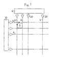
- Figure 1 shows a rectangular array of pixel circuits 2 and circuitry for addressing them.
- the intensity of light to be emitted by a polymer or other organic LED is controlled by varying the current flowing through it. This is done by applying analogue signals, provided by column lines 4 and set up by a column (data arrange) circuit 6, to the pixel circuits 2 on a row-by-row basis.
- the required row 8 is briefly selected by a row select circuit 10 and then deselected. During the selection time slot, the data from the column lines 4 flows into the pixel of the selected row.
- each pixel circuit 2 is isolated from its column line 4 and stores the data that was input. Another set of data is assembled on the column lines 4 and another row 8 is selected. Rows may be selected sequentially or in any desired order.
- Figure 2 shows a generic form of the pixel circuit 2 indicating its operating principle.
- the signal on row 8 operates a voltage-controlled switch 12 to close the switch during the brief selection period and connect column bus line 4 with a node in the circuit whose signal controls an electronically programmable variable resistance 14.
- data flows from the column bus 4 into the pixel circuit 2, current from a global power source 16 flowing through a LED 18 at a value set by the resistance 14.
- the intensity of light output by the LED is controlled in turn by that current. Different light intensities can be set very effectively in the different pixels in this manner.
- Figure 3 shows how the circuit of Figure 2 implemented using MOS (metal-oxide-semiconductor) transistors.
- the voltage controlled switch is formed by a first transistor M1, the gate of which is connected to the row 8.
- the variable resistance is formed by the channel of a second transistor M2, which capacitatively stores charge at its gate to vary the channel resistance depending on the analogue value of the voltage generated by the stored charge. This controls the current in the LED 18 and its light output.
- MOS metal-oxide-semiconductor
- the surface of the substrate is planarised. This planarisation either takes place as part of the manufacturing process of the integrated circuit or as a subsequent customising step.
- the planarisation is effected by depositing a dielectric 30, for example a polymeric material, on the surface of the substrate 32.
- a conducting polymer that can be patterned to create areas of insulation can be used instead for this purpose.
- a metal mirror/electrode 34 which may be of aluminium, for connecting the LED to the appropriate point in the circuit, is then deposited, the connection to the circuit being established by a metallic conducting via 36.
- Metallised portions of the CMOS circuit are designated 38.
- Figure 5 shows an alternative arrangement in which the electrode/mirror 34 is sunk into the dielectric surface, i.e. full planarisation is achieved.
- Appropriate layers 40 of the OLED e.g. polymer or other organic light emitting substance, conducting polymer and the like
- the display is sealed by coating with a glass plate 42.
- Figure 6 shows an alternative display.
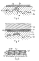
- the planarised aluminium electrode/mirror 34 On the substrate 32 there are deposited, in turn, the planarised aluminium electrode/mirror 34, optionally an electron or hole transport layer 44, a light emitting polymer 46, and a transparent electrode 48.
- the transparent electrode include a layer of conducting polymer 50 and may also include a thin layer of high work function metal 49, of a thickness to be adequately transparent, and a layer of ITO 51.
- An encapsulation layer/barrier 52 which seals all of the LEDs of the array, including their sides, completes this example of the display construction, three pixels of which are shown in Figure 6.
- the flat metal mirrors 34 are applied to the surface of the substrate 32 (preferably a CMOS or bi-CMOS backplane) so as to cover most of the area of each pixel with minimal gaps between the mirrors.
- Chemical Mechanical Polishing may be used to enhance the global and local planarisation.
- the layers of the organic light emitting polymer can be deposited by an automated technique using equipment currently used for applying photo-resists used for the patterning of integrated circuit layers. This gives precise control and a highly uniform thickness for each layer. Alternatively, they could be ink-jet printed. Rare earth organic light emitting chelates can be vacuum deposited.
- the encapsulation layer 52 is applied after making the connections to the transparent electrode in each pixel. Encapsulation, and also possibly the assembly of the pixel, are carried out in clean, dry conditions under a partial vacuum, or a suitable inert or controlled atmosphere.
- the display of the invention may be monochromatic.
- monomeric and polymeric substances are now available which will emit either red, green, blue or white light and can therefore be used to form OLEDs emitting those colours.
- a full colour display can be formed by arranging three individual backplanes, each emitting a different primary monochrome colour, on different sides of an optical system, from another side of which a combined colour image can be viewed.
- polymers or other organic substances emitting different colours can be fabricated so that adjacent diode pixels in groups of three neighbouring pixels produce red, green and blue light.
- field sequential colour filters can be fitted to a white light emitting display.
- Optical systems can also be used for increasing the apparent size of the displayed image, since the physical size of display is limited by the size of the silicon substrate.
- the image can be projected on to a screen.
- the display of the invention is robust, the organic LEDs being well protected, but has simplified manufacture and encapsulation.
- the power generated as heat should be manageable but could be decreased by reducing the current or voltage used to drive each LED. If current routing problems arise, multiple power supply bond pads can be used on the silicon chip.
Claims (29)
- Méthode de fabrication d'un afficheur optoélectronique à diodes électroluminescentes organiques, l'afficheur optoélectronique comprenant un substrat (32) constitué d'une matière semi-conductrice et un réseau de pixels de diodes électroluminescentes organiques (DELO) arrangé sur le substrat, dans laquelle le substrat (32) comprend un circuit actif pour commander la lumière émise par chaque pixel, et chaque pixel comprenant au moins une couche de matière électroluminescente organique (46) et une électrode perméable à la lumière (43, 48) en contact avec la couche organique sur un côté de celle-ci distant du substrat (32), ladite électrode perméable à la lumière (43, 48) comprenant un polymère électriquement conducteur (50), caractérisée en ce que ledit polymère électriquement conducteur est déposé sur une feuille de verre ou de plastique (42, 52) qui est ensuite collée sur la couche de matière électroluminescente organique (46) la plus éloignée du substrat (32).
- Méthode selon la revendication 1, dans laquelle le substrat (32) est constitué de silicium cristallin.
- Méthode selon la revendication 1 ou 2, dans laquelle le substrat (32) présente une surface plane plate.
- Méthode selon la revendication 1 ou 2, dans laquelle le substrat (32) présente une surface non plane.
- Méthode selon la revendication 1, 2 ou 3, comprenant la fourniture d'une électrode métallique (34) en contact avec le substrat (32), ladite électrode métallique servant également de miroir derrière le pixel.
- Méthode selon la revendication 1, 2 ou 3, comprenant la fourniture d'une couche noire d'absorption de la lumière adjacente au substrat (32).
- Méthode selon l'une quelconque des revendications précédentes, dans laquelle l'électrode perméable à la lumière (48) comprend une couche d'oxyde d'étain et indium (ITO) (51).
- Méthode selon l'une quelconque des revendications précédentes, dans laquelle l'électrode perméable à la lumière (48) comprend une couche de métal à travail d'extraction réduit.
- Méthode selon l'une quelconque des revendications 1 à 7, dans laquelle l'électrode perméable à la lumière (48) comprend une couche de métal à travail d'extraction élevé (49).
- Méthode selon la revendication 7, dans laquelle ladite couche ITO (51) est également prévue sous la forme d'un revêtement sur ladite feuille (52).
- Méthode selon l'une quelconque des revendications précédentes, dans laquelle l'électrode perméable à la lumière (48) comprend une couche de résine conductrice à base d'époxy.
- Méthode selon l'une quelconque des revendications précédentes, dans laquelle chaque pixel comprend une électrode inférieure comprenant une couche d'un polymère conducteur.
- Méthode selon l'une quelconque des revendications précédentes, dans laquelle chaque pixel comprend une électrode inférieure comprenant une couche d'un oxyde de métal, tel que l'ITO.
- Méthode selon l'une quelconque des revendications précédentes, dans laquelle chaque pixel comprend une couche de transport d'électrons organique (44) en contact avec la couche de matière électroluminescente (46).
- Méthode selon l'une quelconque des revendications précédentes, dans laquelle chaque pixel comprend une couche de transport de trous organique (44) en contact avec la couche de matière électroluminescente (46).
- Méthode selon l'une quelconque des revendications précédentes, dans laquelle le polymère conducteur (50) est déposé à partir d'une solution de mélange de polymères comprenant au moins un polymère non conducteur.
- Méthode selon l'une quelconque des revendications précédentes, comprenant la fourniture d'une couche extérieure transparente enveloppante imperméable à l'eau et à l'oxygène.
- Méthode selon l'une quelconque des revendications précédentes, dans laquelle la matière électroluminescente est monomère.
- Méthode selon l'une quelconque des revendications 1 à 17, dans laquelle la matière électroluminescente (46) est polymère.
- Méthode selon l'une quelconque des revendications précédentes, dans laquelle chaque DELO comprend un chélate de métal de transition.
- Méthode selon l'une quelconque des revendications précédentes, comprenant la fourniture de moyens (12, 14) pour commander la brillance apparente de la lumière émise par chaque pixel d'une façon analogue.
- Méthode selon la revendication 21, comprenant la fourniture de moyens par lesquels un signal analogique fait varier le rapport marque/espace du cycle opératoire pour lequel la DELO de chaque pixel est mise en circuit.
- Méthode selon la revendication 22, dans laquelle les moyens de commande comprennent un élément à résistance variable dans chaque circuit de pixel (2) pour faire varier le courant à travers la DELO et par conséquent sa sortie d'intensité de lumière.
- Méthode selon la revendication 23, dans laquelle ledit élément à résistance variable comprend le canal d'un transistor à effet de champ semiconducteur à oxyde métallique (MOSFET) (M2).
- Méthode selon la revendication 23 ou 24, dans laquelle chaque circuit de pixel (2) comprend un commutateur à tension commandée (12, M1) pour connecter un signal de données audit élément à résistance variable (14, M2) de façon à régler sa résistance.
- Méthode selon la revendication 25, dans laquelle ledit commutateur comprend un transistor (M1).
- Méthode selon l'une quelconque des revendications précédentes, comprenant la fourniture de groupes répétés de pixels d'émission de rouge, de bleu et de vert pour former une image en couleurs.
- Méthode selon l'une quelconque des revendications précédentes, dans laquelle l'afficheur est arrangé de manière à émettre une lumière blanche, comprenant le réglage de l'afficheur avec des filtres couleurs à séquences de trames pour créer une image en couleurs.
- Méthode pour fabriquer une unité d'affichage en couleurs, comprenant la fabrication de trois afficheurs optoélectroniques, en utilisant dans chaque cas la méthode selon l'une quelconque des revendications 1 à 26, affichant chacun une image dans une couleur monochromatique primaire différente, et en fournissant un système optique pour combiner les trois images en une image en couleurs.
Applications Claiming Priority (3)
| Application Number | Priority Date | Filing Date | Title |
|---|---|---|---|
| GB9907931 | 1999-04-07 | ||
| GBGB9907931.1A GB9907931D0 (en) | 1999-04-07 | 1999-04-07 | An optoelectronic display |
| PCT/GB2000/001295 WO2000060669A1 (fr) | 1999-04-07 | 2000-04-06 | Afficheur optoelectronique |
Publications (2)
| Publication Number | Publication Date |
|---|---|
| EP1177582A1 EP1177582A1 (fr) | 2002-02-06 |
| EP1177582B1 true EP1177582B1 (fr) | 2004-11-03 |
Family
ID=10851086
Family Applications (1)
| Application Number | Title | Priority Date | Filing Date |
|---|---|---|---|
| EP00917184A Expired - Lifetime EP1177582B1 (fr) | 1999-04-07 | 2000-04-06 | Methode de fabrication d'un afficheur optoelectronique a diodes electroluminescentes organiques |
Country Status (7)
| Country | Link |
|---|---|
| US (1) | US6949879B1 (fr) |
| EP (1) | EP1177582B1 (fr) |
| JP (1) | JP2002541631A (fr) |
| AT (1) | ATE281697T1 (fr) |
| DE (1) | DE60015525T2 (fr) |
| GB (1) | GB9907931D0 (fr) |
| WO (1) | WO2000060669A1 (fr) |
Families Citing this family (29)
| Publication number | Priority date | Publication date | Assignee | Title |
|---|---|---|---|---|
| GB0024804D0 (en) * | 2000-10-10 | 2000-11-22 | Microemissive Displays Ltd | An optoelectronic device |
| GB0104961D0 (en) * | 2001-02-28 | 2001-04-18 | Microemissive Displays Ltd | An encapsulated electrode |
| US7682249B2 (en) | 2001-05-04 | 2010-03-23 | Igt | Light emitting interface displays for a gaming machine |
| TWI303533B (en) | 2001-06-15 | 2008-11-21 | Oled T Ltd | Electroluminescent devices |
| GB0116644D0 (en) | 2001-07-09 | 2001-08-29 | Elam T Ltd | Electroluminescent materials and devices |
| US8342938B2 (en) | 2001-09-27 | 2013-01-01 | Igt | Gaming machine reel having a rotatable dynamic display |
| US7628701B2 (en) | 2002-06-24 | 2009-12-08 | Igt | System for interfacing a user and a casino gaming machine |
| GB0222649D0 (en) * | 2002-09-30 | 2002-11-06 | Microemissive Displays Ltd | Passivation layer |
| GB0306721D0 (en) * | 2003-03-24 | 2003-04-30 | Microemissive Displays Ltd | Method of forming a semiconductor device |
| GB0307745D0 (en) * | 2003-04-03 | 2003-05-07 | Microemissive Displays Ltd | Method and apparatus for depositing material on a substrate |
| GB0307746D0 (en) * | 2003-04-03 | 2003-05-07 | Microemissive Displays Ltd | Removing a material from a substrate |
| TWI234124B (en) * | 2003-06-30 | 2005-06-11 | Ritdisplay Corp | Display panel, electrode panel and electrode substrate thereof |
| CN100372145C (zh) * | 2003-09-01 | 2008-02-27 | 友达光电股份有限公司 | 有机发光元件的制造方法及其结构 |
| US8016670B2 (en) | 2004-01-12 | 2011-09-13 | Igt | Virtual glass for a gaming machine |
| GB0524400D0 (en) * | 2005-11-30 | 2006-01-04 | Microemissive Displays Ltd | Temporary memory circuits |
| US8835941B2 (en) * | 2006-02-09 | 2014-09-16 | Qd Vision, Inc. | Displays including semiconductor nanocrystals and methods of making same |
| GB0605014D0 (en) * | 2006-03-13 | 2006-04-19 | Microemissive Displays Ltd | Electroluminescent device |
| CA2540268A1 (fr) * | 2006-03-22 | 2007-09-22 | Realights Inc. | Procede d'eclairage par insertion de diodes electroluminescents dans l'acrylique |
| GB2440368A (en) | 2006-07-26 | 2008-01-30 | Oled T Ltd | Cathode coating for an electroluminescent device |
| JP2010508620A (ja) | 2006-09-12 | 2010-03-18 | キユーデイー・ビジヨン・インコーポレーテツド | 所定のパターンを表示するために有用なエレクトロルミネセントディスプレイ |
| GB0622998D0 (en) * | 2006-11-17 | 2006-12-27 | Microemissive Displays Ltd | Colour optoelectronic device |
| WO2008149874A1 (fr) * | 2007-06-08 | 2008-12-11 | Semiconductor Energy Laboratory Co., Ltd. | Dispositif d'affichage |
| WO2008153087A1 (fr) * | 2007-06-15 | 2008-12-18 | Semiconductor Energy Laboratory Co., Ltd. | Dispositif d'affichage |
| US9525148B2 (en) | 2008-04-03 | 2016-12-20 | Qd Vision, Inc. | Device including quantum dots |
| KR101995369B1 (ko) | 2008-04-03 | 2019-07-02 | 삼성 리서치 아메리카 인코포레이티드 | 양자점들을 포함하는 발광 소자 |
| JP2010145664A (ja) * | 2008-12-17 | 2010-07-01 | Sony Corp | 自発光型表示装置、半導体装置、電子機器及び電源線駆動方法 |
| KR101002659B1 (ko) * | 2008-12-23 | 2010-12-20 | 삼성모바일디스플레이주식회사 | 유기 발광 표시 장치 |
| DE102012223162B4 (de) * | 2012-12-14 | 2022-08-25 | Pictiva Displays International Limited | Flächenlichtsystem |
| US9300292B2 (en) * | 2014-01-10 | 2016-03-29 | Semiconductor Energy Laboratory Co., Ltd. | Circuit including transistor |
Family Cites Families (31)
| Publication number | Priority date | Publication date | Assignee | Title |
|---|---|---|---|---|
| US3710167A (en) * | 1970-07-02 | 1973-01-09 | Rca Corp | Organic electroluminescent cells having a tunnel injection cathode |
| US6331356B1 (en) * | 1989-05-26 | 2001-12-18 | International Business Machines Corporation | Patterns of electrically conducting polymers and their application as electrodes or electrical contacts |
| US5721299A (en) * | 1989-05-26 | 1998-02-24 | International Business Machines Corporation | Electrically conductive and abrasion/scratch resistant polymeric materials, method of fabrication thereof and uses thereof |
| JPH0412494A (ja) * | 1990-04-27 | 1992-01-17 | Sumitomo Chem Co Ltd | 耐湿性el素子 |
| JP3016896B2 (ja) * | 1991-04-08 | 2000-03-06 | パイオニア株式会社 | 有機エレクトロルミネッセンス素子 |
| ATE195197T1 (de) * | 1991-06-12 | 2000-08-15 | Uniax Corp | Anwendbare formen von elektrisch leitfähigen polyanilinen und davon hergestellte leitfähige produkte |
| JPH0520294U (ja) * | 1991-08-28 | 1993-03-12 | スタンレー電気株式会社 | Elセル |
| US5294869A (en) * | 1991-12-30 | 1994-03-15 | Eastman Kodak Company | Organic electroluminescent multicolor image display device |
| US5525867A (en) | 1994-08-05 | 1996-06-11 | Hughes Aircraft Company | Electroluminescent display with integrated drive circuitry |
| JPH08124679A (ja) * | 1994-10-25 | 1996-05-17 | Ibm Japan Ltd | エレクトロ・ルミネッセンス装置 |
| EP0717445B1 (fr) | 1994-12-14 | 2009-06-24 | Eastman Kodak Company | Dispositif électroluminescent avec une couche organique électroluminescente |
| JP3824644B2 (ja) * | 1995-04-18 | 2006-09-20 | ケンブリッジ ディスプレイ テクノロジー リミテッド | 有機発光デバイスの製造 |
| JP2755216B2 (ja) * | 1995-06-20 | 1998-05-20 | 日本電気株式会社 | 有機薄膜el素子の製造方法 |
| US5736754A (en) * | 1995-11-17 | 1998-04-07 | Motorola, Inc. | Full color organic light emitting diode array |
| JPH09306667A (ja) * | 1996-05-21 | 1997-11-28 | Seiko Precision Kk | 有機el素子の製造方法 |
| US6433355B1 (en) * | 1996-06-05 | 2002-08-13 | International Business Machines Corporation | Non-degenerate wide bandgap semiconductors as injection layers and/or contact electrodes for organic electroluminescent devices |
| US5773931A (en) * | 1996-09-06 | 1998-06-30 | Motorola, Inc. | Organic electroluminescent device and method of making same |
| EP0953213A2 (fr) * | 1996-11-12 | 1999-11-03 | International Business Machines Corporation | Motifs de polymeres electroconducteurs et leurs applications comme electrodes ou contacts electriques |
| DE69739633D1 (de) | 1996-11-28 | 2009-12-10 | Casio Computer Co Ltd | Anzeigevorrichtung |
| JPH10161563A (ja) | 1996-11-29 | 1998-06-19 | Tdk Corp | 有機el表示装置 |
| EP0950254A4 (fr) * | 1996-12-23 | 2002-11-27 | Univ Princeton | Dispositif organique luminescent contenant une couche de protection |
| US5739545A (en) * | 1997-02-04 | 1998-04-14 | International Business Machines Corporation | Organic light emitting diodes having transparent cathode structures |
| JP3571171B2 (ja) * | 1997-05-08 | 2004-09-29 | 出光興産株式会社 | 有機エレクトロルミネッセンス素子 |
| US5937272A (en) | 1997-06-06 | 1999-08-10 | Eastman Kodak Company | Patterned organic layers in a full-color organic electroluminescent display array on a thin film transistor array substrate |
| EP0924966A1 (fr) * | 1997-06-30 | 1999-06-23 | Aventis Research & Technologies GmbH & Co. KG | Electrode à couche mince pour dispositifs électroluminescentes organiques plains et procédé de fabrication |
| JPH1154268A (ja) * | 1997-08-08 | 1999-02-26 | Sanyo Electric Co Ltd | 有機エレクトロルミネッセンスディスプレイ装置 |
| JPH1167448A (ja) * | 1997-08-26 | 1999-03-09 | Toyota Central Res & Dev Lab Inc | ディスプレイ装置 |
| US5877695A (en) * | 1997-10-07 | 1999-03-02 | Ericsson, Inc. | Visual alarm for a communication module |
| US5998805A (en) * | 1997-12-11 | 1999-12-07 | Motorola, Inc. | Active matrix OED array with improved OED cathode |
| EP1055260A1 (fr) * | 1998-02-02 | 2000-11-29 | Uniax Corporation | Diodes organiques a photosensibilite commutable |
| GB0024804D0 (en) * | 2000-10-10 | 2000-11-22 | Microemissive Displays Ltd | An optoelectronic device |
-
1999
- 1999-04-07 GB GBGB9907931.1A patent/GB9907931D0/en not_active Ceased
-
2000
- 2000-04-06 DE DE60015525T patent/DE60015525T2/de not_active Expired - Fee Related
- 2000-04-06 JP JP2000610069A patent/JP2002541631A/ja active Pending
- 2000-04-06 EP EP00917184A patent/EP1177582B1/fr not_active Expired - Lifetime
- 2000-04-06 WO PCT/GB2000/001295 patent/WO2000060669A1/fr active IP Right Grant
- 2000-04-06 US US09/958,102 patent/US6949879B1/en not_active Expired - Fee Related
- 2000-04-06 AT AT00917184T patent/ATE281697T1/de not_active IP Right Cessation
Also Published As
| Publication number | Publication date |
|---|---|
| GB9907931D0 (en) | 1999-06-02 |
| JP2002541631A (ja) | 2002-12-03 |
| US6949879B1 (en) | 2005-09-27 |
| DE60015525D1 (de) | 2004-12-09 |
| DE60015525T2 (de) | 2005-10-27 |
| ATE281697T1 (de) | 2004-11-15 |
| WO2000060669A1 (fr) | 2000-10-12 |
| EP1177582A1 (fr) | 2002-02-06 |
Similar Documents
| Publication | Publication Date | Title |
|---|---|---|
| EP1177582B1 (fr) | Methode de fabrication d'un afficheur optoelectronique a diodes electroluminescentes organiques | |
| JP4254240B2 (ja) | 有機エレクトロルミネッセントディスプレイおよび電子装置 | |
| US10497757B2 (en) | Display device | |
| US6091194A (en) | Active matrix display | |
| US7580014B2 (en) | Display apparatus | |
| US7190122B2 (en) | OLED display with improved active matrix circuitry | |
| US7642109B2 (en) | Electrical connection in OLED devices | |
| US7187118B2 (en) | Dual panel type organic electro luminescent display device and manufacturing method for the same | |
| JP3850005B2 (ja) | スイッチング素子及び有機エレクトロルミネッセンス素子表示装置 | |
| EP2151865A1 (fr) | Dispositif électroluminescent, appareil électroluminescent, et leurs procédés de production | |
| KR19990072868A (ko) | 디스플레이소자 | |
| JP2004281399A (ja) | El表示素子 | |
| KR20010041040A (ko) | 전자 발광 소자 | |
| KR20090033425A (ko) | 액티브 매트릭스 유기 전자-광학 디바이스, 픽셀로 이루어진 디스플레이 및 이것의 구동 방법 | |
| KR20070091331A (ko) | 표시 패널 및 이를 제조하는 방법 | |
| US8278828B1 (en) | Large area organic LED display | |
| KR20110112309A (ko) | 변조 가능한 발광 다이오드 | |
| JP2005513555A (ja) | アクティブマトリクスエレクトロルミネッセンス表示装置 | |
| US7638949B2 (en) | Organic electroluminescence device, method for driving thereof, and electronic appliance | |
| US6815710B2 (en) | Organic electroluminescence unit | |
| US20020190664A1 (en) | Organic EL element, organic EL element array and organic EL display | |
| US7714514B1 (en) | Large area organic electroluminescent display using bimorph MEMS devices | |
| US10211268B1 (en) | Large area OLED display | |
| US10529279B1 (en) | Large area OLED display with MEMS switching device | |
| JP4314000B2 (ja) | 表示装置 |
Legal Events
| Date | Code | Title | Description |
|---|---|---|---|
| PUAI | Public reference made under article 153(3) epc to a published international application that has entered the european phase |
Free format text: ORIGINAL CODE: 0009012 |
|
| 17P | Request for examination filed |
Effective date: 20011119 |
|
| AK | Designated contracting states |
Kind code of ref document: A1 Designated state(s): AT BE CH CY DE DK ES FI FR GB GR IE IT LI LU MC NL PT SE |
|
| GRAP | Despatch of communication of intention to grant a patent |
Free format text: ORIGINAL CODE: EPIDOSNIGR1 |
|
| RTI1 | Title (correction) |
Free format text: METHOD OF MAKING AN OPTOELECTRONIC ORGANIC LIGHT EMITTING DIODE DISPLAY |
|
| GRAP | Despatch of communication of intention to grant a patent |
Free format text: ORIGINAL CODE: EPIDOSNIGR1 |
|
| GRAP | Despatch of communication of intention to grant a patent |
Free format text: ORIGINAL CODE: EPIDOSNIGR1 |
|
| GRAS | Grant fee paid |
Free format text: ORIGINAL CODE: EPIDOSNIGR3 |
|
| GRAA | (expected) grant |
Free format text: ORIGINAL CODE: 0009210 |
|
| AK | Designated contracting states |
Kind code of ref document: B1 Designated state(s): AT BE CH CY DE DK ES FI FR GB GR IE IT LI LU MC NL PT SE |
|
| PG25 | Lapsed in a contracting state [announced via postgrant information from national office to epo] |
Ref country code: IT Free format text: LAPSE BECAUSE OF FAILURE TO SUBMIT A TRANSLATION OF THE DESCRIPTION OR TO PAY THE FEE WITHIN THE PRE;WARNING: LAPSES OF ITALIAN PATENTS WITH EFFECTIVE DATE BEFORE 2007 MAY HAVE OCCURRED AT ANY TIME BEFORE 2007. THE CORRECT EFFECTIVE DATE MAY BE DIFFERENT FROM THE ONE RECORDED.SCRIBED TIME-LIMIT Effective date: 20041103 Ref country code: CH Free format text: LAPSE BECAUSE OF FAILURE TO SUBMIT A TRANSLATION OF THE DESCRIPTION OR TO PAY THE FEE WITHIN THE PRESCRIBED TIME-LIMIT Effective date: 20041103 Ref country code: FI Free format text: LAPSE BECAUSE OF FAILURE TO SUBMIT A TRANSLATION OF THE DESCRIPTION OR TO PAY THE FEE WITHIN THE PRESCRIBED TIME-LIMIT Effective date: 20041103 Ref country code: NL Free format text: LAPSE BECAUSE OF FAILURE TO SUBMIT A TRANSLATION OF THE DESCRIPTION OR TO PAY THE FEE WITHIN THE PRESCRIBED TIME-LIMIT Effective date: 20041103 Ref country code: LI Free format text: LAPSE BECAUSE OF FAILURE TO SUBMIT A TRANSLATION OF THE DESCRIPTION OR TO PAY THE FEE WITHIN THE PRESCRIBED TIME-LIMIT Effective date: 20041103 Ref country code: BE Free format text: LAPSE BECAUSE OF FAILURE TO SUBMIT A TRANSLATION OF THE DESCRIPTION OR TO PAY THE FEE WITHIN THE PRESCRIBED TIME-LIMIT Effective date: 20041103 Ref country code: AT Free format text: LAPSE BECAUSE OF FAILURE TO SUBMIT A TRANSLATION OF THE DESCRIPTION OR TO PAY THE FEE WITHIN THE PRESCRIBED TIME-LIMIT Effective date: 20041103 |
|
| REG | Reference to a national code |
Ref country code: GB Ref legal event code: FG4D |
|
| REG | Reference to a national code |
Ref country code: CH Ref legal event code: EP |
|
| REF | Corresponds to: |
Ref document number: 60015525 Country of ref document: DE Date of ref document: 20041209 Kind code of ref document: P |
|
| REG | Reference to a national code |
Ref country code: IE Ref legal event code: FG4D |
|
| PG25 | Lapsed in a contracting state [announced via postgrant information from national office to epo] |
Ref country code: GR Free format text: LAPSE BECAUSE OF FAILURE TO SUBMIT A TRANSLATION OF THE DESCRIPTION OR TO PAY THE FEE WITHIN THE PRESCRIBED TIME-LIMIT Effective date: 20050203 Ref country code: DK Free format text: LAPSE BECAUSE OF FAILURE TO SUBMIT A TRANSLATION OF THE DESCRIPTION OR TO PAY THE FEE WITHIN THE PRESCRIBED TIME-LIMIT Effective date: 20050203 Ref country code: SE Free format text: LAPSE BECAUSE OF FAILURE TO SUBMIT A TRANSLATION OF THE DESCRIPTION OR TO PAY THE FEE WITHIN THE PRESCRIBED TIME-LIMIT Effective date: 20050203 |
|
| PG25 | Lapsed in a contracting state [announced via postgrant information from national office to epo] |
Ref country code: ES Free format text: LAPSE BECAUSE OF FAILURE TO SUBMIT A TRANSLATION OF THE DESCRIPTION OR TO PAY THE FEE WITHIN THE PRESCRIBED TIME-LIMIT Effective date: 20050214 |
|
| PG25 | Lapsed in a contracting state [announced via postgrant information from national office to epo] |
Ref country code: CY Free format text: LAPSE BECAUSE OF FAILURE TO SUBMIT A TRANSLATION OF THE DESCRIPTION OR TO PAY THE FEE WITHIN THE PRESCRIBED TIME-LIMIT Effective date: 20050406 Ref country code: LU Free format text: LAPSE BECAUSE OF NON-PAYMENT OF DUE FEES Effective date: 20050406 Ref country code: IE Free format text: LAPSE BECAUSE OF NON-PAYMENT OF DUE FEES Effective date: 20050406 |
|
| PG25 | Lapsed in a contracting state [announced via postgrant information from national office to epo] |
Ref country code: MC Free format text: LAPSE BECAUSE OF NON-PAYMENT OF DUE FEES Effective date: 20050430 |
|
| NLV1 | Nl: lapsed or annulled due to failure to fulfill the requirements of art. 29p and 29m of the patents act | ||
| REG | Reference to a national code |
Ref country code: CH Ref legal event code: PL |
|
| PLBE | No opposition filed within time limit |
Free format text: ORIGINAL CODE: 0009261 |
|
| STAA | Information on the status of an ep patent application or granted ep patent |
Free format text: STATUS: NO OPPOSITION FILED WITHIN TIME LIMIT |
|
| ET | Fr: translation filed | ||
| 26N | No opposition filed |
Effective date: 20050804 |
|
| PG25 | Lapsed in a contracting state [announced via postgrant information from national office to epo] |
Ref country code: PT Free format text: LAPSE BECAUSE OF NON-PAYMENT OF DUE FEES Effective date: 20050403 |
|
| PGFP | Annual fee paid to national office [announced via postgrant information from national office to epo] |
Ref country code: DE Payment date: 20091013 Year of fee payment: 10 |
|
| PGFP | Annual fee paid to national office [announced via postgrant information from national office to epo] |
Ref country code: GB Payment date: 20091022 Year of fee payment: 10 Ref country code: FR Payment date: 20091112 Year of fee payment: 10 |
|
| GBPC | Gb: european patent ceased through non-payment of renewal fee |
Effective date: 20100406 |
|
| REG | Reference to a national code |
Ref country code: FR Ref legal event code: ST Effective date: 20101230 |
|
| PG25 | Lapsed in a contracting state [announced via postgrant information from national office to epo] |
Ref country code: DE Free format text: LAPSE BECAUSE OF NON-PAYMENT OF DUE FEES Effective date: 20101103 |
|
| PG25 | Lapsed in a contracting state [announced via postgrant information from national office to epo] |
Ref country code: GB Free format text: LAPSE BECAUSE OF NON-PAYMENT OF DUE FEES Effective date: 20100406 |
|
| PG25 | Lapsed in a contracting state [announced via postgrant information from national office to epo] |
Ref country code: FR Free format text: LAPSE BECAUSE OF NON-PAYMENT OF DUE FEES Effective date: 20100430 |