EP1172854A2 - Halbleiterspeicher mit wahlfreiem Zugriff - Google Patents
Halbleiterspeicher mit wahlfreiem Zugriff Download PDFInfo
- Publication number
- EP1172854A2 EP1172854A2 EP01114531A EP01114531A EP1172854A2 EP 1172854 A2 EP1172854 A2 EP 1172854A2 EP 01114531 A EP01114531 A EP 01114531A EP 01114531 A EP01114531 A EP 01114531A EP 1172854 A2 EP1172854 A2 EP 1172854A2
- Authority
- EP
- European Patent Office
- Prior art keywords
- lines
- column
- row lines
- memory
- memory matrix
- Prior art date
- Legal status (The legal status is an assumption and is not a legal conclusion. Google has not performed a legal analysis and makes no representation as to the accuracy of the status listed.)
- Withdrawn
Links
Images






Classifications
-
- G—PHYSICS
- G11—INFORMATION STORAGE
- G11C—STATIC STORES
- G11C11/00—Digital stores characterised by the use of particular electric or magnetic storage elements; Storage elements therefor
- G11C11/02—Digital stores characterised by the use of particular electric or magnetic storage elements; Storage elements therefor using magnetic elements
- G11C11/14—Digital stores characterised by the use of particular electric or magnetic storage elements; Storage elements therefor using magnetic elements using thin-film elements
- G11C11/15—Digital stores characterised by the use of particular electric or magnetic storage elements; Storage elements therefor using magnetic elements using thin-film elements using multiple magnetic layers
-
- G—PHYSICS
- G11—INFORMATION STORAGE
- G11C—STATIC STORES
- G11C11/00—Digital stores characterised by the use of particular electric or magnetic storage elements; Storage elements therefor
- G11C11/02—Digital stores characterised by the use of particular electric or magnetic storage elements; Storage elements therefor using magnetic elements
- G11C11/16—Digital stores characterised by the use of particular electric or magnetic storage elements; Storage elements therefor using magnetic elements using elements in which the storage effect is based on magnetic spin effect
-
- G—PHYSICS
- G11—INFORMATION STORAGE
- G11C—STATIC STORES
- G11C7/00—Arrangements for writing information into, or reading information out from, a digital store
- G11C7/18—Bit line organisation; Bit line lay-out
-
- H—ELECTRICITY
- H10—SEMICONDUCTOR DEVICES; ELECTRIC SOLID-STATE DEVICES NOT OTHERWISE PROVIDED FOR
- H10B—ELECTRONIC MEMORY DEVICES
- H10B61/00—Magnetic memory devices, e.g. magnetoresistive RAM [MRAM] devices
Definitions
- the invention relates to memory matrices, in particular memory matrices for MRAMs, i.e. non-volatile magnetic memory elements made of magnetic tunnel elements, according to Preamble of claim 1.
- Semiconductors with random access usually have a cell field from a matrix of column and row lines at the intersections of which there is one Memory cell is located.
- An MRAM uses memory elements typically used magnetic tunnel elements.
- Such a TMR element (TMR: tunnel magnetic resistance; English: tunneling magneto resistance) basically consists of two magnetic layers, a hard magnetic and a soft magnetic Layer. These are due to an insulating intermediate layer with a thickness of only a few atomic layers from each other Cut. The magnetizations in the two layers can be both rectified and directed towards each other. The insulating barrier between the magnetic layers is like this thin that after applying a voltage a few electrons through it can get; a so-called tunnel current flows. The strength of the tunnel current depends on the orientation the directions of magnetization to each other.
- the respective adjacent lines change their arrangements in the direction of travel means that at least one of the adjacent lines changes with respect to one line. This means that a line does not have the same neighboring lines across the entire cell array. With simultaneous addressing of neighboring lines, as is usually the case with Address decoders occurs, this is advantageous because undesirable coupling effects between two lines can be reduced.
- this change of arrangement consists of juxtaposed lines in that two each Lines are crossed because there is a crossover of two Technologically, it is easiest to implement neighboring lines is.
- An embodiment of the invention is that the Memory matrix has a first and second cell field, which are stacked on top of each other, with the Columns or row lines from different locations in the are essentially opposite. Such a stack has the The advantage that the storage density per chip area increases leaves.
- a line is multiple with any one and not always the same one at a time adjacent column or row lines crossed will, i.e. swaps their order. This can be another Reduction of the coupling values between the originally next to each other arranged lines can be reached.
- the change of Arrangement of different side by side Columns or row lines only with each other in a partial area the column and row lines that are used for a memory access is activated.
- This is advantageous because having so a small number of changes in arrangement, if possible high decoupling between the lines of the sub-area is achieved can be. It is sufficient to just couple within of these segments, i.e. several side by side or logically assigned lines to reduce, because the segments are only addressed one after the other. Only at the same time addressed lines can influence each other. Have unswitched or de-energized lines no significant influence on the switching properties of the active lines. The active lines also affect not the contents of the storage elements on the neighboring ones inactive lines. Nevertheless, a relatively good decoupling achieved for a variety of possible bit patterns.
- the memory matrix with respect to the changes in the arrangement of their lines so is constructed so that the order of the column or row lines on opposite edges of the memory matrix is equal to.
- This can result in additional circuitry be avoided when implementing address decoders, which arises when the address lines are disordered or have an order that differs from the original. This is particularly important because in In the case of MRAM memories, a connection of the column and Row lines on both edges of the cell field are useful is.
- the Cell fields or their column or row lines with regard to their changes in arrangement are mirror-symmetrical.
- edge area of the cell field Includes lines that do not change their arrangements.
- Fig. 1a is a TMR element according to the prior art pictured, with M1 and M2 the column and row lines for addressing, describing and reading out a Represent storage element.
- M1 and M2 the column and row lines for addressing, describing and reading out a Represent storage element.
- By stacking several such storage elements can be the storage density increase per chip area.
- Fig. 1b this is for two layers shown.
- another column line level M3 inserted.
- a stack of more than two TMR elements is conceivable.
- write currents flow through the column lines 4, 5, 6 and 7 and by a row line 7, so the four memory cells marked by circles to be discribed.
- a "zero" or logical "One" to be written is the flow direction of the Current through the column lines negative or positive and thus the respective magnetization rectified or opposite for magnetizing the hard magnetic layer directed.
- Fig. 2 is in the column lines 4 and 6 a “one" and in the column lines 5 and 7 one Inscribed "zero".
- a non-volatile magnetic Semiconductor memory from a matrix of columns S and Row lines Z built up. At the intersection of everyone Column S and row line Z is the TMR element.
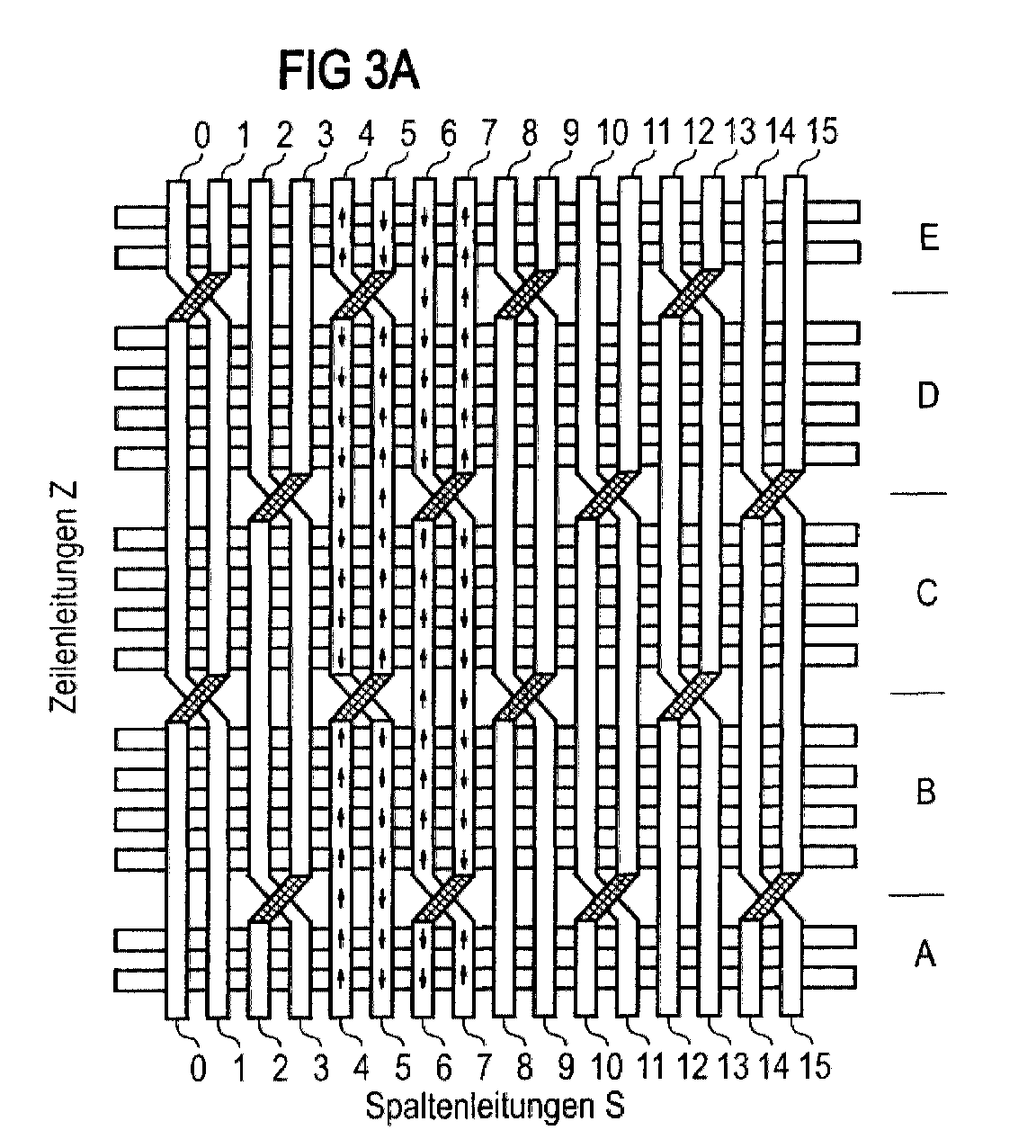
- two each Adjacent column lines S one or more times with each other crosses, so that these further their positions To deceive. As already explained above, this changes for a crossed line at least one of its direct Neighboring lines.
- Example marked by the mark A causes the Crossing of lines 2 and 3 that the Constellation of neighboring lines for lines 1,2,3 and 4 changes at the same time.
- column lines 4 and 5 of 3a Looking closely at column lines 4 and 5 of 3a can be seen that the courses of the Column lines 4 and 5 cross each other twice. As well are the adjacent column line pairs 2 and 3 or 6 and 7 crossed so that their place Crossovers to the crossings of the column lines 4 and 5 are offset. This has the consequence that in the shown embodiment the neighboring lines of Column lines 4 and 5 four times across sectors A to E. change.
- Coupling value for the edge lines (4 and 7) from -16 and for the cables (5 and 6) in the middle have a coupling value of - 32nd
- FIG. 4a Another embodiment is shown in Fig. 4a.
- this crossover scheme means that the Order of the column lines at the top of the matrix is not identical to that at the bottom.
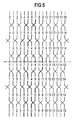
- 4a is the order of the column lines at the top of the cell matrix disordered and one Address decoders are therefore difficult to implement. This Disadvantage can be remedied by having two Cell fields with the same crossover scheme is a mirror image of each other. This is shown in Fig. 5 shown schematically, the dashed line represents imaginary mirror line.
- the order of Column lines S at the top correspond to the order the column lines S at the bottom.
- crossovers only occur within several or lines arranged one above the other. This can be useful because a memory access is carried out in blocks and only the side by side or one above the other arranged column lines are activated at the same time.
- Figures 6a-6h show the crossover in a packet of four column lines.
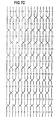
- the lines shown thinly here correspond to a logical "zero" or a negative current flow, the thick lines to a logical "one" or a positive current flow. It can be seen that there is a relatively uniform distribution of adjacent and non-adjacent areas and of the edge areas for all the bit patterns shown. The four lines are therefore decoupled relatively well for all possible bit patterns. This favorable constellation is achieved for four lines after two crossings (FIG. 7a), for eight lines four crossings are necessary (FIG. 7b), for 16 lines eight crossings (FIG. 7c) or generally for 2 n lines 2 n-1 crossovers. This can reduce the number of crossovers and at the same time ensure a good and even reduction in the cross coupling.
- FIG. 8a shows an embodiment in which two cell fields are stacked on top of each other, i.e. there is a row level M2 and two column levels M1, M3.
- the column lines M1-1, M3-1 and M1-2 of levels M1 and M2 each run over the entire Length parallel to each other.
- the column lines M1-1 and M3-1 are crossed with one another led so that the column lines M3-1 and M3-2 only half of their lengths are directly adjacent, whereby the coupling between these two lines is reduced becomes.
- MRAM memories can also be implemented with more than two layers become, the concept of crossing one another Column lines or row lines are also appropriate applicable accordingly.
- crossovers within a cell level also with crossovers can be combined between two cell levels.
Landscapes
- Engineering & Computer Science (AREA)
- Computer Hardware Design (AREA)
- Semiconductor Memories (AREA)
- Mram Or Spin Memory Techniques (AREA)
- Static Random-Access Memory (AREA)
- Hall/Mr Elements (AREA)
Abstract
Description
Adressdecodierern vorkommt, ist dies von Vorteil, weil somit unerwünschte Überkopplungseffekte zwischen zwei Leitungen reduziert werden können.
- Fig. 1a
- ein magnetisches TMR-Element nach dem Stand der Technik;
- Fig. 1b
- zwei magnetische TMR-Elemente, die in zwei Lagen übereinander angeordnet sind;
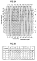
- Tab. 2a
- einen Ausschnitt aus einem Zellenfeld ohne Überkreuzung der Leitungen nach dem Stand der Technik;
- Fig. 2b
- eine Tabelle, die die Größenordnungen der Überkopplungen zwischen den Spaltenleitungen bei einem Zellenfeld nach Fig. 2a darstellt;
- Fig. 3a
- einen Ausschnitt aus einem Zellenfeld mit Überkreuzung von jeweils zwei benachbarter Spaltenleitungen;
- Tab. 3b
- eine Tabelle, die die Größenordnung der Überkopplung zwischen den Spaltenleitungen bei einem Zellenfeld nach Fig. 3a darstellt;
- Fig. 4a
- einen Ausschnitt aus einem Zellenfeld mit mehrfacher Überkreuzung von mehreren Bitleitungen;
- Tab. 4b
- eine Tabelle, die die Größenordnungen der Überkopplungen zwischen den Spaltenleitungen bei einem Zellenfeld nach Fig. 4a darstellt;
- Fig. 5
- eine spiegelsymmetrische Anordnung von zwei Zellenfeldern gemäß Fig. 4a, wobei die Reihenfolge der Spaltenleitungen am oberen Rand gleich der am unteren Rand entspricht;
- Fig. 6a-6h
- ein Paket von vier Spaltenleitungen, die bei einem Speicherzugriff gemeinsam aktiviert werden, wobei die Spaltenleitungen nur innerhalb dieses Pakets überkreuzt sind;
- Fig. 7a-7c
- günstige Überkreuzungskonstellationen bei Paketgrößen von 4, 8 bzw. 16 Spaltenleitungen;
- Fig. 8a
- eine mögliche Anordnung zweier Zellenfelder, bei der jeweils zwei Speicherelemente übereinander gestapelt sind;
- Fig. 8b
- zwei Zellenfelder nach Fig. 8a mit Spaltenleitungen, die miteinander überkreuzt sind.
Claims (9)
- Speichermatrix, die mindestens ein Zellenfeld aus Spaltenleitungen und Zeilenleitungen aufweist, an deren Schnittpunkten sich jeweils Speicherelemente befinden, wobei jeweils die Zeilenleitungen und/oder die Spaltenleitungen eines Zellenfelds nebeneinander angeordnet sind,
dadurch gekennzeichnet, dass mindestens zwei Spalten- oder Zeilenleitungen ihre Anordnung zueinander ändern. - Speichermatrix nach Anspruch 1, dadurch gekennzeichnet, dass die mindestens zwei Spalten- oder Zeilenleitungen überkreuzt sind.
- Speichermatrix nach einem der Ansprüche 1 oder 2, dadurch gekennzeichnet, dass die Speicherelemente nichtflüchtige magnetische TMR-Elemente sind.
- Speichermatrix nach einem der vorangehenden Ansprüche, dadurch gekennzeichnet, dass sie ein erstes und ein zweites Zellenfeld aufweist, die in Lagen übereinander gestapelt sind, wobei jeweils die Spalten- bzw. Zeilenleitungen von verschiedenen Lagen sich im wesentlichen benachbart gegenüberliegen.
- Speichermatrix nach einem der vorangehenden Ansprüche, dadurch gekennzeichnet, dass mindestens eine der Spaltenbzw. Zeilenleitungen über ihre Länge mehrfach mit mindestens zwei verschiedenen, nebeneinander angeordneten und/oder einander gegenüberliegenden Spalten- bzw. Zeilenleitung überkreuzt ist.
- Speichermatrix nach einem der vorangehenden Ansprüche, dadurch gekennzeichnet, dass benachbarte Spalten- bzw. Zeilenleitungen jeweils nur innerhalb eines bei einem Speicherzugriff gleichzeitig aktivierten Teilbereichs von Spalten- bzw. Zeilenleitungen miteinander überkreuzt sind.
- Speichermatrix nach einem der vorangehenden Ansprüche, dadurch gekennzeichnet, dass mindestens eines der Zellenfelder so aufgebaut ist, so dass die Reihenfolge der Spalten- bzw. Zeilenleitungen an gegenüberliegenden Rändern der Speichermatrix gleich ist.
- Speichermatrix nach Anspruch 7, dadurch gekennzeichnet, dass mindestens eines der Zellenfelder hinsichtlich der Anordnungen der Spalten- und/oder der Zeilenleitungen spiegelsymmetrisch ist.
- Speichermatrix nach einem der vorangehenden Ansprüche, dadurch gekennzeichnet, dass im Randbereich eines der Zellenfelder keine Änderung der Anordnung der Spalten- oder Zeilenleitungen erfolgt.
Applications Claiming Priority (2)
| Application Number | Priority Date | Filing Date | Title |
|---|---|---|---|
| DE10034083 | 2000-07-13 | ||
| DE10034083A DE10034083C1 (de) | 2000-07-13 | 2000-07-13 | Halbleiterspeicher mit wahlfreiem Zugeriff mit reduziertem Signalüberkoppeln |
Publications (2)
| Publication Number | Publication Date |
|---|---|
| EP1172854A2 true EP1172854A2 (de) | 2002-01-16 |
| EP1172854A3 EP1172854A3 (de) | 2006-01-18 |
Family
ID=7648809
Family Applications (1)
| Application Number | Title | Priority Date | Filing Date |
|---|---|---|---|
| EP01114531A Withdrawn EP1172854A3 (de) | 2000-07-13 | 2001-06-16 | Halbleiterspeicher mit wahlfreiem Zugriff |
Country Status (7)
| Country | Link |
|---|---|
| US (1) | US6826075B2 (de) |
| EP (1) | EP1172854A3 (de) |
| JP (1) | JP2002134708A (de) |
| KR (1) | KR100442460B1 (de) |
| CN (1) | CN1207716C (de) |
| DE (1) | DE10034083C1 (de) |
| TW (1) | TWI278097B (de) |
Cited By (1)
| Publication number | Priority date | Publication date | Assignee | Title |
|---|---|---|---|---|
| DE10309244A1 (de) * | 2003-03-03 | 2004-09-23 | Siemens Ag | Magnetisches Speicherelement, insbesondere MRAM-Element, mit einem TMR-Dünnschichtensystem |
Families Citing this family (6)
| Publication number | Priority date | Publication date | Assignee | Title |
|---|---|---|---|---|
| JP4637388B2 (ja) * | 2001-03-23 | 2011-02-23 | ルネサスエレクトロニクス株式会社 | 薄膜磁性体記憶装置 |
| US7020008B2 (en) | 2001-12-26 | 2006-03-28 | Renesas Technology Corp. | Thin film magnetic memory device writing data with bidirectional current |
| JP2004023062A (ja) * | 2002-06-20 | 2004-01-22 | Nec Electronics Corp | 半導体装置とその製造方法 |
| US11251019B2 (en) * | 2016-12-15 | 2022-02-15 | Toyota Jidosha Kabushiki Kaisha | Plasma device |
| JP6863199B2 (ja) | 2017-09-25 | 2021-04-21 | トヨタ自動車株式会社 | プラズマ処理装置 |
| KR102565822B1 (ko) * | 2018-12-04 | 2023-08-11 | 에스케이하이닉스 주식회사 | 반도체 장치 |
Family Cites Families (14)
| Publication number | Priority date | Publication date | Assignee | Title |
|---|---|---|---|---|
| US3471839A (en) * | 1965-09-14 | 1969-10-07 | Ibm | Storage sensing system for a magnetic matrix employing two storage elements per bit |
| US3604109A (en) * | 1969-11-17 | 1971-09-14 | Thomas & Betts Corp | Method of making horseshoe-shaped keepered word-line structure for memory planes |
| US4238838A (en) * | 1978-05-16 | 1980-12-09 | Ampex Corporation | Core memory wiring arrangement |
| CA1305255C (en) * | 1986-08-25 | 1992-07-14 | Joseph Lebowitz | Marching interconnecting lines in semiconductor integrated circuits |
| JPH0713858B2 (ja) | 1988-08-30 | 1995-02-15 | 三菱電機株式会社 | 半導体記憶装置 |
| US5732010A (en) * | 1992-09-22 | 1998-03-24 | Kabushiki Kaisha Toshiba | Dynamic random access memory device with the combined open/folded bit-line pair arrangement |
| KR100215595B1 (ko) * | 1993-09-21 | 1999-08-16 | 니시무로 타이죠 | 다이나믹형 반도체 기억장치 |
| US5640343A (en) * | 1996-03-18 | 1997-06-17 | International Business Machines Corporation | Magnetic memory array using magnetic tunnel junction devices in the memory cells |
| JP3345549B2 (ja) | 1996-04-26 | 2002-11-18 | ティーディーケイ株式会社 | 磁気抵抗効果メモリ |
| KR100270577B1 (ko) * | 1996-08-30 | 2000-11-01 | 김영환 | 플래쉬 메모리 셀의 제조 방법 |
| TW411471B (en) * | 1997-09-17 | 2000-11-11 | Siemens Ag | Memory-cell device |
| US5982658A (en) * | 1997-10-31 | 1999-11-09 | Honeywell Inc. | MRAM design to reduce dissimilar nearest neighbor effects |
| KR100277888B1 (ko) * | 1997-12-31 | 2001-02-01 | 김영환 | 플래쉬메모리및그의제조방법 |
| US6259621B1 (en) * | 2000-07-06 | 2001-07-10 | Micron Technology, Inc. | Method and apparatus for minimization of data line coupling in a semiconductor memory device |
-
2000
- 2000-07-13 DE DE10034083A patent/DE10034083C1/de not_active Expired - Fee Related
-
2001
- 2001-06-16 EP EP01114531A patent/EP1172854A3/de not_active Withdrawn
- 2001-07-10 KR KR10-2001-0041197A patent/KR100442460B1/ko not_active Expired - Fee Related
- 2001-07-11 JP JP2001211245A patent/JP2002134708A/ja active Pending
- 2001-07-12 TW TW090117072A patent/TWI278097B/zh not_active IP Right Cessation
- 2001-07-13 CN CNB011231114A patent/CN1207716C/zh not_active Expired - Fee Related
- 2001-09-24 US US09/905,853 patent/US6826075B2/en not_active Expired - Fee Related
Cited By (1)
| Publication number | Priority date | Publication date | Assignee | Title |
|---|---|---|---|---|
| DE10309244A1 (de) * | 2003-03-03 | 2004-09-23 | Siemens Ag | Magnetisches Speicherelement, insbesondere MRAM-Element, mit einem TMR-Dünnschichtensystem |
Also Published As
| Publication number | Publication date |
|---|---|
| KR100442460B1 (ko) | 2004-07-30 |
| TWI278097B (en) | 2007-04-01 |
| KR20020009411A (ko) | 2002-02-01 |
| US20020012266A1 (en) | 2002-01-31 |
| US6826075B2 (en) | 2004-11-30 |
| CN1333538A (zh) | 2002-01-30 |
| DE10034083C1 (de) | 2002-03-14 |
| CN1207716C (zh) | 2005-06-22 |
| EP1172854A3 (de) | 2006-01-18 |
| JP2002134708A (ja) | 2002-05-10 |
Similar Documents
| Publication | Publication Date | Title |
|---|---|---|
| EP1184871B1 (de) | MRAM-Anordnung | |
| EP1354321B1 (de) | Mram-anordnung | |
| DE69924655T2 (de) | Magnetische Tunnelübergangsvorrichtungen | |
| DE10196802B4 (de) | Rauschunterdrückung für DRAM-Architekturen mit offener Bitleitung | |
| DE69927487T2 (de) | Verfahren zum Schreiben und Lesen von magnetoresistiven Speichern | |
| DE10314812A1 (de) | Magnetische Kleinbereichs-Speichervorrichtungen | |
| DE10032271C2 (de) | MRAM-Anordnung | |
| DE60307459T2 (de) | Mram-zelle und speicherarchitektur mit maximalem lesesignal und reduzierter elektromagnetischer interferenz | |
| DE10355273A1 (de) | Magnetische Speichervorichtungen mit wahlfreiem Zugang (MRAM) mit nicht parallelen Haupt- und Bezugs-Magnetwiderständen | |
| DE60304209T2 (de) | Magnettunnelsperrschichtspeicherzellenarchitektur | |
| EP1360692B1 (de) | Verfahren zum beschreiben magnetoresistiver speicherzellen und mit diesem verfahren beschreibbarer magnetoresistiver speicher | |
| DE19823826A1 (de) | MRAM-Speicher sowie Verfahren zum Lesen/Schreiben digitaler Information in einen derartigen Speicher | |
| EP1222662B1 (de) | Mehrwertiger magnetoresistiver schreib/lese-speicher sowie verfahren zum beschreiben und auslesen eines solchen speichers | |
| DE10034083C1 (de) | Halbleiterspeicher mit wahlfreiem Zugeriff mit reduziertem Signalüberkoppeln | |
| EP1174924A2 (de) | MRAM-Speicherzelle | |
| DE10056830C2 (de) | Integrierte magnetoresistive Halbleiterspeicheranordnung | |
| EP1187137B1 (de) | MRAM-Modulanordnung | |
| DE60207006T2 (de) | Magneto-resistiver Film und Speicher mit diesem Film | |
| DE102004030174A1 (de) | Verfahren zur Herstellung magnetischer Direktzugriffsspeicher | |
| WO2002084705A2 (de) | Verfahren zum betrieb einer mram-halbleiterspeicheranordnung | |
| EP1342242B1 (de) | Mram-anordnung mit auswahltransistoren grosser kanalweite | |
| DE102005004593B4 (de) | Integrierter Halbleiterspeicher mit einer Anordnung nichtflüchtiger Speicherzellen | |
| DE60223161T2 (de) | Stromquelle und drainanordnung für magnetoresitive speicher | |
| DE102004031140B4 (de) | MRAM-Speichervorrichtung | |
| DE10393096T5 (de) | Magnetspeicher unter Verwendung eines ferromagnetischen Tunnelübergangselements |
Legal Events
| Date | Code | Title | Description |
|---|---|---|---|
| PUAI | Public reference made under article 153(3) epc to a published international application that has entered the european phase |
Free format text: ORIGINAL CODE: 0009012 |
|
| AK | Designated contracting states |
Kind code of ref document: A2 Designated state(s): AT BE CH CY DE DK ES FI FR GB GR IE IT LI LU MC NL PT SE TR |
|
| AX | Request for extension of the european patent |
Free format text: AL;LT;LV;MK;RO;SI |
|
| PUAL | Search report despatched |
Free format text: ORIGINAL CODE: 0009013 |
|
| AK | Designated contracting states |
Kind code of ref document: A3 Designated state(s): AT BE CH CY DE DK ES FI FR GB GR IE IT LI LU MC NL PT SE TR |
|
| AX | Request for extension of the european patent |
Extension state: AL LT LV MK RO SI |
|
| RIC1 | Information provided on ipc code assigned before grant |
Ipc: H01L 23/522 20060101ALI20051128BHEP Ipc: H01L 21/768 20060101ALI20051128BHEP Ipc: G11C 11/16 20060101ALI20051128BHEP Ipc: G11C 7/18 20060101ALI20051128BHEP Ipc: H01L 27/22 20060101AFI20051128BHEP |
|
| 17P | Request for examination filed |
Effective date: 20051215 |
|
| AKX | Designation fees paid |
Designated state(s): DE FR GB IE IT |
|
| 17Q | First examination report despatched |
Effective date: 20071106 |
|
| RAP1 | Party data changed (applicant data changed or rights of an application transferred) |
Owner name: INFINEON TECHNOLOGIES AG |
|
| STAA | Information on the status of an ep patent application or granted ep patent |
Free format text: STATUS: THE APPLICATION IS DEEMED TO BE WITHDRAWN |
|
| 18D | Application deemed to be withdrawn |
Effective date: 20100323 |