EP1172661B1 - Switchable testing circuit for single-ended and differential termination - Google Patents
Switchable testing circuit for single-ended and differential termination Download PDFInfo
- Publication number
- EP1172661B1 EP1172661B1 EP01105970A EP01105970A EP1172661B1 EP 1172661 B1 EP1172661 B1 EP 1172661B1 EP 01105970 A EP01105970 A EP 01105970A EP 01105970 A EP01105970 A EP 01105970A EP 1172661 B1 EP1172661 B1 EP 1172661B1
- Authority
- EP
- European Patent Office
- Prior art keywords
- circuit
- nodes
- diode bridge
- elements
- resistor
- Prior art date
- Legal status (The legal status is an assumption and is not a legal conclusion. Google has not performed a legal analysis and makes no representation as to the accuracy of the status listed.)
- Expired - Lifetime
Links
- 239000000872 buffer Substances 0.000 claims description 23
- 101100102849 Saccharomyces cerevisiae (strain ATCC 204508 / S288c) VTH1 gene Proteins 0.000 description 2
- 101150088150 VTH2 gene Proteins 0.000 description 2
- 230000005540 biological transmission Effects 0.000 description 2
- 230000001419 dependent effect Effects 0.000 description 1
- 239000004065 semiconductor Substances 0.000 description 1
Images

Classifications
-
- G—PHYSICS
- G01—MEASURING; TESTING
- G01R—MEASURING ELECTRIC VARIABLES; MEASURING MAGNETIC VARIABLES
- G01R31/00—Arrangements for testing electric properties; Arrangements for locating electric faults; Arrangements for electrical testing characterised by what is being tested not provided for elsewhere
- G01R31/28—Testing of electronic circuits, e.g. by signal tracer
- G01R31/317—Testing of digital circuits
- G01R31/3181—Functional testing
- G01R31/319—Tester hardware, i.e. output processing circuits
- G01R31/31917—Stimuli generation or application of test patterns to the device under test [DUT]
- G01R31/31924—Voltage or current aspects, e.g. driver, receiver
-
- G—PHYSICS
- G01—MEASURING; TESTING
- G01R—MEASURING ELECTRIC VARIABLES; MEASURING MAGNETIC VARIABLES
- G01R31/00—Arrangements for testing electric properties; Arrangements for locating electric faults; Arrangements for electrical testing characterised by what is being tested not provided for elsewhere
- G01R31/28—Testing of electronic circuits, e.g. by signal tracer
- G01R31/317—Testing of digital circuits
- G01R31/3181—Functional testing
- G01R31/319—Tester hardware, i.e. output processing circuits
- G01R31/3193—Tester hardware, i.e. output processing circuits with comparison between actual response and known fault free response
Definitions
- the invention relates to an electronic circuit for automatic test equipment for testing a device under test.
- test equipment is generally known and widely used for testing a variety of different electronic devices.
- the test equipment as disclosed e.g. in US-A-5,101,153, comprises a so-called pin-electronic circuit for generating input signals to the device under test.
- This circuit also has to represent a correct termination for the device under test and, finally, must be capable to analyze the response signals from the device under test.
- the device under test may have one physical signal line for any one of the logical signals. This case is called single-ended.
- the pin-electronic circuit may be terminated e.g. via a resistor to a programmable voltage.
- the device under test has differential output signals, i.e. two lines per signal.
- the pin-electronic circuit may be terminated with one resistor at each line of the differential signal wherein the two resistors of the two lines are programmed to the same voltage. This is called a differential signal operation with single-ended termination.
- the pin-electronic circuit may be terminated with one resistor between both lines of the differential signal. This is called a differential signal operation with differential termination.
- the invention provides the advantage that one and the same circuit may be used for an independent single-ended termination of any of the lines of the device under test, for a differential signal operation with single-ended termination and for a differential signal operation with differential termination.
- one and the same circuit may be used for different devices under test. Or in other words: It is not necessary anymore to provide different circuits for these different devices under test. The effort and the costs in connection with the automatic test equipment are therefore reduced.
- a diode bridge is used to switch between the different modes of the electronic circuit according to the invention.
- This diode bridge has the advantage that the automatic test equipment may be implemented for high-frequency applications because it can be made on one semiconductor chip, which minimizes physical distances.
- Figure 1 shows a first embodiment of an electronic circuit for an automatic test equipment according to the invention
- figure 2 shows a second embodiment of an electronic circuit according to the invention
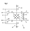
- figure 3 shows a third embodiment of an electronic circuit according to the invention.
- FIG 1 a first embodiment of a pin-electronic circuit 10 for an automatic test equipment according to the invention is shown.
- a signal SIG_A from a device under test is received by the circuit 10 on a line 11 and a signal SIG_B from the same device under test is received by the circuit 10 on a line 12.
- One input of a comparator CS1 is connected to the line 11 and one input of a comparator CS2 is connected to the line 12.
- the respective other inputs of the comparators CS1, CS2 receive a voltage VTH1, VTH2.
- the two inputs of another comparator CD are connected to the two lines 11, 12.
- Each of the two lines 11, 12 are also connected to a resistor R1, R2 which both have the impedance Z of each of the transmission lines from the device under test to the circuit 10.
- the other sides of two resistors R1, R2 are then connected together via a switch SW.
- Two buffers B1, B2 generate voltages VT1, VT2 at their outputs.
- the value of these voltages VT1, VT2 may be varied by voltages VT01, VT02 at the inputs of the buffers B1, B2.
- the outputs of the buffers B1, B2 are connected to the resistors R1, R2 at both sides of the switch SW.
- the voltages VT1, VT2 of the buffers B1, B2, therefore, constitute respective terminations for the two lines 11, 12.
- the buffers B1, B2 may be switched into a high-impedance state with the signals HZ1, HZ2.
- the circuit 10 of figure 1 provides a single-ended termination for the lines 11, 12.
- the line 11 and the line 12 are independent of each other.
- the line 11 may be terminated with the voltage VT1 by the buffer B1.
- the signal SIG_A of the line 11 may be compared with the voltage VTH1 by the comparator CS1.
- the buffer B2 may be switched into a high-impedance state and the signal SIG_B of the line 12 may be compared with the voltage VTH2 by the comparator CS2.
- the comparator CD is inactive.
- the circuit 10 of figure 1 provides a differential signal operation with a single-ended termination.
- the two comparators CS1, CS2 are inactive and the two signals SIG_A, SIG_B are compared by the comparator CD.
- the comparison may be performed by the two comparators CS1, CS2 with the comparator CD being inactive.
- the circuit 10 of figure 1 provides a differential signal operation with a differential termination.
- the two comparators CS1, CS2 are inactive and the two signals SIG_A, SIG_B are compared by the comparator CD.
- Figure 2 shows a second embodiment of a pin-electronic circuit 20 of an automatic test equipment according to the invention.
- the circuit 20 of figure 2 is similar to the circuit 10 of figure 1. Therefore, corresponding features are depicted with the same reference characters.
- the switch SW of figure 1 is replaced by a diode bridge 21 and two switched current sources 22, 23.
- the diode bridge 21 comprises four diodes D1, D2, D3, D4.
- a serial connection of a current source I1 and a switch SW1 is connected to the anodes of the diodes D1, D2.
- the cathodes of the diodes D3, D4 are connected to a serial connection of a switch SW2 and a current source I2.
- the cathode of the diode D1 is connected to the anode of the diode D3 and both are connected to a connection point of two resistors R10, R11.
- the other side of the resistor R10 is connected to the output of the buffer B1 and the other side of the resistor R11 is connected to the line 11.
- the cathode of the diode D2 is connected to the anode of the diode D4 and both are connected to a connection point of two resistors R20, R21.
- the other side of the resistor R20 is connected to the output of the buffer B2 and the other side of the resistor R21 is connected to the line 12.
- the two switches SW1, SW2 may be switched with the help of a common signal DT.
- the diode bridge 21 is used in its resistive region so that it acts as a small resistor.
- the circuit 20 of figure 2 provides a single-ended termination for the two lines 11, 12.
- the comparators CS1, CS2 are active whereas the diode bridge 21 and the comparator CD are inactive.
- the termination of each of the two lines 11, 12 may be programmed differently by the input voltages VT01, VT02 of the buffers B1, B2.
- the resistors R10, R11 and the resistors R20, R21 may be selected such that they result in the impedance Z of each of the transmission lines from the device under test to the two lines 11, 12.
- the circuit 20 of figure 2 provides a differential signal operation with single-ended termination.
- the circuit 20 of figure 2 provides a differential signal operation with differential termination of the lines 11, 12.
- the diode bridge 21 and the comparator CD are active whereas the comparators CS1, CS2 are inactive.
- the diode bridge 21 may also be used in its non-resistive region so that it acts as a so-called active or programmable load for one of the two lines 11, 12.
- the two switches SW1, SW2 are closed and e.g. the buffer B1 is set into its high-impedance state and the buffer B2 is set into its low-impedance state at a first voltage. If e.g. the line 11 carries a second voltage, then the voltage difference between the first and the second voltage is present at the diode bridge 21.
- the diode bridge 21 represents a load, which is programmable in particular with the first voltage and therefore the output voltage of the buffer B2.
- Figure 3 shows a third embodiment of a pin-electronic circuit 30 of an automatic test equipment according to the invention.
- the circuit 30 of figure 3 is similar to the circuit 20 of figure 2. Therefore, corresponding features are depicted with the same reference characters.
- the two buffers B1, B2 of figure 1 are replaced by two drivers DR1, DR2.
- Each of these drivers DR1, DR2 has an input, which may be programmed with a voltage DATA1, DATA2.
- the voltages DATA1, DATA2 may be programmed identical to the voltages VT01, VT02 as described in connection with the circuit 20 of figure 2.
- the drivers DR1, DR2 of the circuit 30 of figure 3 are used to establish a termination for the two lines 11, 12. This mode, therefore, is used for receiving the signals SIG_A, SIG_B on the lines 11, 12 from the device under test.
- the two drivers DR1, DR2 may also be used to send signals via the two lines 11, 12 to the device under test, in particular a logical low level signal or a logical high level signal.
- the inputs DATA1, DATA2 of the drivers DR1, DR2 are programmed as desired by a specific test program included in the automatic test equipment.
Landscapes
- Engineering & Computer Science (AREA)
- General Engineering & Computer Science (AREA)
- Physics & Mathematics (AREA)
- General Physics & Mathematics (AREA)
- Tests Of Electronic Circuits (AREA)
- Dc Digital Transmission (AREA)
- Logic Circuits (AREA)
Priority Applications (4)
| Application Number | Priority Date | Filing Date | Title |
|---|---|---|---|
| DE60100109T DE60100109T2 (de) | 2001-03-10 | 2001-03-10 | Umschaltbare Testschaltung für asymmetrischen und differentiellen Abschluss |
| EP01105970A EP1172661B1 (en) | 2001-03-10 | 2001-03-10 | Switchable testing circuit for single-ended and differential termination |
| US09/999,315 US6639397B2 (en) | 2001-03-10 | 2001-10-31 | Automatic test equipment for testing a device under test |
| JP2002051316A JP4171229B2 (ja) | 2001-03-10 | 2002-02-27 | 自動試験装置の電子回路 |
Applications Claiming Priority (1)
| Application Number | Priority Date | Filing Date | Title |
|---|---|---|---|
| EP01105970A EP1172661B1 (en) | 2001-03-10 | 2001-03-10 | Switchable testing circuit for single-ended and differential termination |
Publications (2)
| Publication Number | Publication Date |
|---|---|
| EP1172661A1 EP1172661A1 (en) | 2002-01-16 |
| EP1172661B1 true EP1172661B1 (en) | 2003-02-19 |
Family
ID=8176740
Family Applications (1)
| Application Number | Title | Priority Date | Filing Date |
|---|---|---|---|
| EP01105970A Expired - Lifetime EP1172661B1 (en) | 2001-03-10 | 2001-03-10 | Switchable testing circuit for single-ended and differential termination |
Country Status (4)
| Country | Link |
|---|---|
| US (1) | US6639397B2 (https=) |
| EP (1) | EP1172661B1 (https=) |
| JP (1) | JP4171229B2 (https=) |
| DE (1) | DE60100109T2 (https=) |
Families Citing this family (21)
| Publication number | Priority date | Publication date | Assignee | Title |
|---|---|---|---|---|
| US6798237B1 (en) | 2001-08-29 | 2004-09-28 | Altera Corporation | On-chip impedance matching circuit |
| US6812732B1 (en) | 2001-12-04 | 2004-11-02 | Altera Corporation | Programmable parallel on-chip parallel termination impedance and impedance matching |
| US6836144B1 (en) | 2001-12-10 | 2004-12-28 | Altera Corporation | Programmable series on-chip termination impedance and impedance matching |
| US6812734B1 (en) | 2001-12-11 | 2004-11-02 | Altera Corporation | Programmable termination with DC voltage level control |
| US7109744B1 (en) | 2001-12-11 | 2006-09-19 | Altera Corporation | Programmable termination with DC voltage level control |
| DE10207676A1 (de) * | 2002-02-22 | 2003-09-04 | Philips Intellectual Property | Schaltungsanordnung für einen stromgesteuerten Widerstand mit erweitertem Linearitätsbereich |
| US6888369B1 (en) | 2003-07-17 | 2005-05-03 | Altera Corporation | Programmable on-chip differential termination impedance |
| DE10338030B3 (de) * | 2003-08-19 | 2005-04-28 | Infineon Technologies Ag | Integrierte Schaltung zum Testen von Schaltungskomponenten eines Halbleiterchips |
| US6888370B1 (en) | 2003-08-20 | 2005-05-03 | Altera Corporation | Dynamically adjustable termination impedance control techniques |
| US6859064B1 (en) | 2003-08-20 | 2005-02-22 | Altera Corporation | Techniques for reducing leakage current in on-chip impedance termination circuits |
| US20050146320A1 (en) * | 2003-12-31 | 2005-07-07 | Gohel Tushar K. | Differential active load |
| US7218155B1 (en) | 2005-01-20 | 2007-05-15 | Altera Corporation | Techniques for controlling on-chip termination resistance using voltage range detection |
| US7221193B1 (en) | 2005-01-20 | 2007-05-22 | Altera Corporation | On-chip termination with calibrated driver strength |
| US7679397B1 (en) | 2005-08-05 | 2010-03-16 | Altera Corporation | Techniques for precision biasing output driver for a calibrated on-chip termination circuit |
| ATE434189T1 (de) * | 2006-03-09 | 2009-07-15 | Teradyne Inc | V/i-quelle und testsystem damit |
| US7408406B2 (en) * | 2006-05-24 | 2008-08-05 | Tektronix, Inc. | Mode selection amplifier circuit usable in a signal acquisition probe |
| DE102007045756B4 (de) * | 2007-09-25 | 2014-05-15 | Texas Instruments Deutschland Gmbh | Elektronische Leiterplatte und Verfahren für das automatische Prüfen |
| US8278936B2 (en) * | 2007-11-23 | 2012-10-02 | Evan Grund | Test circuits and current pulse generator for simulating an electrostatic discharge |
| US8836383B2 (en) * | 2012-09-07 | 2014-09-16 | Richtek Technology Corporation | Multipurpose half bridge signal output circuit |
| US9813050B1 (en) * | 2016-04-13 | 2017-11-07 | Analog Devices, Inc. | Comparator circuit with input attenuator |
| US10145893B2 (en) | 2016-12-25 | 2018-12-04 | Nuvoton Technology Corporation | Resolving automated test equipment (ATE) timing constraint violations |
Family Cites Families (13)
| Publication number | Priority date | Publication date | Assignee | Title |
|---|---|---|---|---|
| US4646299A (en) * | 1983-08-01 | 1987-02-24 | Fairchild Semiconductor Corporation | Method and apparatus for applying and monitoring programmed test signals during automated testing of electronic circuits |
| FR2648943B1 (fr) * | 1989-06-23 | 1991-10-11 | Radiotechnique Compelec | Circuit echantillonneur-bloqueur |
| US5010297A (en) * | 1989-12-01 | 1991-04-23 | Analog Devices, Incorporated | Automatic test equipment with active load having high-speed inhibit mode switching |
| US5200696A (en) * | 1990-09-10 | 1993-04-06 | Ltx Corporation | Test system apparatus with Schottky diodes with programmable voltages |
| US5101153A (en) * | 1991-01-09 | 1992-03-31 | National Semiconductor Corporation | Pin electronics test circuit for IC device testing |
| US5521493A (en) * | 1994-11-21 | 1996-05-28 | Megatest Corporation | Semiconductor test system including a novel driver/load circuit |
| JP3331109B2 (ja) * | 1996-01-23 | 2002-10-07 | 株式会社アドバンテスト | 半導体試験装置の比較器 |
| JP3672136B2 (ja) * | 1996-10-04 | 2005-07-13 | 株式会社アドバンテスト | Ic試験装置 |
| US5942922A (en) * | 1998-04-07 | 1999-08-24 | Credence Systems Corporation | Inhibitable, continuously-terminated differential drive circuit for an integrated circuit tester |
| JP3872594B2 (ja) * | 1998-05-21 | 2007-01-24 | 株式会社アドバンテスト | 半導体試験装置 |
| US6313657B1 (en) * | 1998-12-24 | 2001-11-06 | Advantest Corporation | IC testing apparatus and testing method using same |
| US6211723B1 (en) * | 1999-01-20 | 2001-04-03 | Ltx Corporation | Programmable load circuit for use in automatic test equipment |
| US6275023B1 (en) * | 1999-02-03 | 2001-08-14 | Hitachi Electronics Engineering Co., Ltd. | Semiconductor device tester and method for testing semiconductor device |
-
2001
- 2001-03-10 EP EP01105970A patent/EP1172661B1/en not_active Expired - Lifetime
- 2001-03-10 DE DE60100109T patent/DE60100109T2/de not_active Expired - Lifetime
- 2001-10-31 US US09/999,315 patent/US6639397B2/en not_active Expired - Fee Related
-
2002
- 2002-02-27 JP JP2002051316A patent/JP4171229B2/ja not_active Expired - Fee Related
Also Published As
| Publication number | Publication date |
|---|---|
| EP1172661A1 (en) | 2002-01-16 |
| US6639397B2 (en) | 2003-10-28 |
| JP2002311108A (ja) | 2002-10-23 |
| DE60100109T2 (de) | 2003-10-16 |
| JP4171229B2 (ja) | 2008-10-22 |
| DE60100109D1 (de) | 2003-03-27 |
| US20020125896A1 (en) | 2002-09-12 |
Similar Documents
| Publication | Publication Date | Title |
|---|---|---|
| EP1172661B1 (en) | Switchable testing circuit for single-ended and differential termination | |
| US7138846B2 (en) | Field effect transistor switch circuit | |
| US6275023B1 (en) | Semiconductor device tester and method for testing semiconductor device | |
| US6605958B2 (en) | Precision on-chip transmission line termination | |
| US6353334B1 (en) | Circuit for converting a logic signal on an output node to a pair of low-voltage differential signals | |
| US7313723B2 (en) | Self-reparable semiconductor and method thereof | |
| US7772912B2 (en) | Level shift circuit and method thereof | |
| CA2227890A1 (en) | Universal sender device | |
| US20020075035A1 (en) | Circuit for providing a logical output signal in accordance with crossing points of differential signals | |
| US6166569A (en) | Test interface circuits with waveform synthesizers having reduced spurious signals | |
| US6292010B1 (en) | Dynamic pin driver combining high voltage mode and high speed mode | |
| US6930506B2 (en) | Terminating resistor driver for high speed data communication | |
| EP1380113B1 (en) | Means for compensating a data-dependent supply current in an electronic circuit | |
| US7215148B1 (en) | Programmable current output buffer | |
| US6242966B1 (en) | Leakage current correcting circuit | |
| JPH03179920A (ja) | サンプルホールド回路装置 | |
| JP3208002B2 (ja) | 信号処理装置及びレベル変換回路 | |
| EP1386402B1 (en) | Modified repetitive cell matching technique for integrated circuits | |
| US20070241822A1 (en) | Chain-chopping current mirror and method for stabilizing output currents | |
| CN112731120B (zh) | 复合引脚驱动器 | |
| US6693464B2 (en) | Low-voltage current mode logic circuits and methods | |
| JPH06260915A (ja) | マルチプレクサ装置 | |
| US20070018638A1 (en) | Electrical test circuit with active-load and output sampling capability | |
| US6437633B2 (en) | Switching element, stage and system | |
| CN1191642A (zh) | 去复用器、保护转换单元、电信网络和去复用方法 |
Legal Events
| Date | Code | Title | Description |
|---|---|---|---|
| PUAI | Public reference made under article 153(3) epc to a published international application that has entered the european phase |
Free format text: ORIGINAL CODE: 0009012 |
|
| 17P | Request for examination filed |
Effective date: 20011023 |
|
| AK | Designated contracting states |
Kind code of ref document: A1 Designated state(s): DE FR GB Kind code of ref document: A1 Designated state(s): AT BE CH CY DE DK ES FI FR GB GR IE IT LI LU MC NL PT SE TR |
|
| AX | Request for extension of the european patent |
Free format text: AL;LT;LV;MK;RO;SI |
|
| 17Q | First examination report despatched |
Effective date: 20020228 |
|
| GRAH | Despatch of communication of intention to grant a patent |
Free format text: ORIGINAL CODE: EPIDOS IGRA |
|
| AKX | Designation fees paid |
Free format text: DE FR GB |
|
| RTI1 | Title (correction) |
Free format text: SWITCHABLE TESTING CIRCUIT FOR SINGLE-ENDED AND DIFFERENTIAL TERMINATION |
|
| GRAH | Despatch of communication of intention to grant a patent |
Free format text: ORIGINAL CODE: EPIDOS IGRA |
|
| GRAA | (expected) grant |
Free format text: ORIGINAL CODE: 0009210 |
|
| AK | Designated contracting states |
Designated state(s): DE FR GB |
|
| PG25 | Lapsed in a contracting state [announced via postgrant information from national office to epo] |
Ref country code: FR Free format text: LAPSE BECAUSE OF FAILURE TO SUBMIT A TRANSLATION OF THE DESCRIPTION OR TO PAY THE FEE WITHIN THE PRESCRIBED TIME-LIMIT Effective date: 20030219 |
|
| REG | Reference to a national code |
Ref country code: GB Ref legal event code: FG4D |
|
| REG | Reference to a national code |
Ref country code: IE Ref legal event code: FG4D |
|
| REF | Corresponds to: |
Ref document number: 60100109 Country of ref document: DE Date of ref document: 20030327 Kind code of ref document: P |
|
| PLBE | No opposition filed within time limit |
Free format text: ORIGINAL CODE: 0009261 |
|
| STAA | Information on the status of an ep patent application or granted ep patent |
Free format text: STATUS: NO OPPOSITION FILED WITHIN TIME LIMIT |
|
| EN | Fr: translation not filed | ||
| REG | Reference to a national code |
Ref country code: IE Ref legal event code: MM4A |
|
| 26N | No opposition filed |
Effective date: 20031120 |
|
| PGFP | Annual fee paid to national office [announced via postgrant information from national office to epo] |
Ref country code: GB Payment date: 20070307 Year of fee payment: 7 |
|
| GBPC | Gb: european patent ceased through non-payment of renewal fee |
Effective date: 20080310 |
|
| PG25 | Lapsed in a contracting state [announced via postgrant information from national office to epo] |
Ref country code: GB Free format text: LAPSE BECAUSE OF NON-PAYMENT OF DUE FEES Effective date: 20080310 |
|
| REG | Reference to a national code |
Ref country code: DE Ref legal event code: R082 Ref document number: 60100109 Country of ref document: DE Representative=s name: SCHOPPE, ZIMMERMANN, STOECKELER, ZINKLER & PAR, DE |
|
| REG | Reference to a national code |
Ref country code: DE Ref legal event code: R082 Ref document number: 60100109 Country of ref document: DE Representative=s name: SCHOPPE, ZIMMERMANN, STOECKELER, ZINKLER & PAR, DE Effective date: 20120515 Ref country code: DE Ref legal event code: R081 Ref document number: 60100109 Country of ref document: DE Owner name: ADVANTEST (SINGAPORE) PTE. LTD., SG Free format text: FORMER OWNER: VERIGY (SINGAPORE) PTE. LTD., SINGAPORE, SG Effective date: 20120515 Ref country code: DE Ref legal event code: R082 Ref document number: 60100109 Country of ref document: DE Representative=s name: SCHOPPE, ZIMMERMANN, STOECKELER, ZINKLER, SCHE, DE Effective date: 20120515 |
|
| PGFP | Annual fee paid to national office [announced via postgrant information from national office to epo] |
Ref country code: DE Payment date: 20140417 Year of fee payment: 14 |
|
| REG | Reference to a national code |
Ref country code: DE Ref legal event code: R119 Ref document number: 60100109 Country of ref document: DE |
|
| PG25 | Lapsed in a contracting state [announced via postgrant information from national office to epo] |
Ref country code: DE Free format text: LAPSE BECAUSE OF NON-PAYMENT OF DUE FEES Effective date: 20151001 |