EP1168433A2 - Verfahren zur Herstellung einer Verbindungsstruktur in einer Halbleitervorrichtung - Google Patents
Verfahren zur Herstellung einer Verbindungsstruktur in einer Halbleitervorrichtung Download PDFInfo
- Publication number
- EP1168433A2 EP1168433A2 EP01305540A EP01305540A EP1168433A2 EP 1168433 A2 EP1168433 A2 EP 1168433A2 EP 01305540 A EP01305540 A EP 01305540A EP 01305540 A EP01305540 A EP 01305540A EP 1168433 A2 EP1168433 A2 EP 1168433A2
- Authority
- EP
- European Patent Office
- Prior art keywords
- film
- wiring
- dielectric constant
- interlayer insulating
- insulating film
- Prior art date
- Legal status (The legal status is an assumption and is not a legal conclusion. Google has not performed a legal analysis and makes no representation as to the accuracy of the status listed.)
- Withdrawn
Links
Images

Classifications
-
- H—ELECTRICITY
- H10—SEMICONDUCTOR DEVICES; ELECTRIC SOLID-STATE DEVICES NOT OTHERWISE PROVIDED FOR
- H10W—GENERIC PACKAGES, INTERCONNECTIONS, CONNECTORS OR OTHER CONSTRUCTIONAL DETAILS OF DEVICES COVERED BY CLASS H10
- H10W20/00—Interconnections in chips, wafers or substrates
- H10W20/01—Manufacture or treatment
-
- H—ELECTRICITY
- H10—SEMICONDUCTOR DEVICES; ELECTRIC SOLID-STATE DEVICES NOT OTHERWISE PROVIDED FOR
- H10P—GENERIC PROCESSES OR APPARATUS FOR THE MANUFACTURE OR TREATMENT OF DEVICES COVERED BY CLASS H10
- H10P14/00—Formation of materials, e.g. in the shape of layers or pillars
- H10P14/60—Formation of materials, e.g. in the shape of layers or pillars of insulating materials
- H10P14/68—Organic materials, e.g. photoresists
-
- H—ELECTRICITY
- H10—SEMICONDUCTOR DEVICES; ELECTRIC SOLID-STATE DEVICES NOT OTHERWISE PROVIDED FOR
- H10P—GENERIC PROCESSES OR APPARATUS FOR THE MANUFACTURE OR TREATMENT OF DEVICES COVERED BY CLASS H10
- H10P14/00—Formation of materials, e.g. in the shape of layers or pillars
- H10P14/60—Formation of materials, e.g. in the shape of layers or pillars of insulating materials
- H10P14/63—Formation of materials, e.g. in the shape of layers or pillars of insulating materials characterised by the formation processes
- H10P14/6326—Deposition processes
- H10P14/6328—Deposition from the gas or vapour phase
- H10P14/6334—Deposition from the gas or vapour phase using decomposition or reaction of gaseous or vapour phase compounds, i.e. chemical vapour deposition
- H10P14/6336—Deposition from the gas or vapour phase using decomposition or reaction of gaseous or vapour phase compounds, i.e. chemical vapour deposition in the presence of a plasma [PECVD]
-
- H—ELECTRICITY
- H10—SEMICONDUCTOR DEVICES; ELECTRIC SOLID-STATE DEVICES NOT OTHERWISE PROVIDED FOR
- H10P—GENERIC PROCESSES OR APPARATUS FOR THE MANUFACTURE OR TREATMENT OF DEVICES COVERED BY CLASS H10
- H10P14/00—Formation of materials, e.g. in the shape of layers or pillars
- H10P14/60—Formation of materials, e.g. in the shape of layers or pillars of insulating materials
- H10P14/66—Formation of materials, e.g. in the shape of layers or pillars of insulating materials characterised by the type of materials
- H10P14/668—Formation of materials, e.g. in the shape of layers or pillars of insulating materials characterised by the type of materials the materials being characterised by the deposition precursor materials
-
- H—ELECTRICITY
- H10—SEMICONDUCTOR DEVICES; ELECTRIC SOLID-STATE DEVICES NOT OTHERWISE PROVIDED FOR
- H10W—GENERIC PACKAGES, INTERCONNECTIONS, CONNECTORS OR OTHER CONSTRUCTIONAL DETAILS OF DEVICES COVERED BY CLASS H10
- H10W20/00—Interconnections in chips, wafers or substrates
- H10W20/01—Manufacture or treatment
- H10W20/071—Manufacture or treatment of dielectric parts thereof
- H10W20/074—Manufacture or treatment of dielectric parts thereof of dielectric parts comprising thin functional dielectric layers, e.g. dielectric etch-stop, barrier, capping or liner layers
- H10W20/077—Manufacture or treatment of dielectric parts thereof of dielectric parts comprising thin functional dielectric layers, e.g. dielectric etch-stop, barrier, capping or liner layers on sidewalls or on top surfaces of conductors
-
- H—ELECTRICITY
- H10—SEMICONDUCTOR DEVICES; ELECTRIC SOLID-STATE DEVICES NOT OTHERWISE PROVIDED FOR
- H10W—GENERIC PACKAGES, INTERCONNECTIONS, CONNECTORS OR OTHER CONSTRUCTIONAL DETAILS OF DEVICES COVERED BY CLASS H10
- H10W20/00—Interconnections in chips, wafers or substrates
- H10W20/01—Manufacture or treatment
- H10W20/071—Manufacture or treatment of dielectric parts thereof
- H10W20/081—Manufacture or treatment of dielectric parts thereof by forming openings in the dielectric parts
- H10W20/084—Manufacture or treatment of dielectric parts thereof by forming openings in the dielectric parts for dual-damascene structures
- H10W20/088—Manufacture or treatment of dielectric parts thereof by forming openings in the dielectric parts for dual-damascene structures involving partial etching of via holes
-
- H—ELECTRICITY
- H10—SEMICONDUCTOR DEVICES; ELECTRIC SOLID-STATE DEVICES NOT OTHERWISE PROVIDED FOR
- H10W—GENERIC PACKAGES, INTERCONNECTIONS, CONNECTORS OR OTHER CONSTRUCTIONAL DETAILS OF DEVICES COVERED BY CLASS H10
- H10W20/00—Interconnections in chips, wafers or substrates
- H10W20/40—Interconnections external to wafers or substrates, e.g. back-end-of-line [BEOL] metallisations or vias connecting to gate electrodes
- H10W20/45—Interconnections external to wafers or substrates, e.g. back-end-of-line [BEOL] metallisations or vias connecting to gate electrodes characterised by their insulating parts
- H10W20/48—Insulating materials thereof
-
- H—ELECTRICITY
- H10—SEMICONDUCTOR DEVICES; ELECTRIC SOLID-STATE DEVICES NOT OTHERWISE PROVIDED FOR
- H10W—GENERIC PACKAGES, INTERCONNECTIONS, CONNECTORS OR OTHER CONSTRUCTIONAL DETAILS OF DEVICES COVERED BY CLASS H10
- H10W20/00—Interconnections in chips, wafers or substrates
- H10W20/40—Interconnections external to wafers or substrates, e.g. back-end-of-line [BEOL] metallisations or vias connecting to gate electrodes
- H10W20/495—Capacitive arrangements or effects of, or between wiring layers
Definitions
- the present invention relates to a method of manufacturing semiconductor devices.
- a method of manufacturing semiconductor devices having a dual damascene structure wiring is a method of manufacturing semiconductor devices having a dual damascene structure wiring.
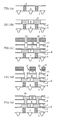
- an interlayer insulating film 22 made of BPSG (boron-phosphorus-silicate glass) is formed on a semiconductor substrate 21 having a transistor (not shown) formed thereon.
- a contact hole is formed in this interlayer insulating film 22.
- a tungsten film is formed and its surface is polished by a CMP method so that a tungsten plug 23 is buried in the contact hole.
- an etching stop film 24 is deposited and a non-fluorinated organic polymer film 25 having a dielectric constant of 3.0 is formed thereon.
- a trench is formed for a damascene wiring structure, and copper is buried in the damascene wiring trench to form a first layer copper wiring 26.
- a copper diffusion inhibiting film 27 is formed by a plasma CVD method on the non-fluorinated organic polymer film 25 and the first layer copper wiring 26, and thereon are formed a non-fluorinated organic polymer film 28, a copper diffusion inhibiting film 29, a non-fluorinated organic polymer film 30 and an etching stop film 31.
- a contact hole 33 for connecting the first copper wiring 26 and the second wiring is formed by dry etching using a resist mask 32 having a predetermined shape.
- a wiring trench 35 is formed by dry etching using a resist mask 34 having a predetermined shape so as to include the contact hole 33.
- copper is buried in the contact hole 33 and the wiring trench 35 to form a copper dual damascene wiring 36.
- the etching stop films in order to control the depth of the wiring trenches in dry etching for forming the wiring trenches in the interlayer insulating films because the depth of the trenches directly affects the wiring resistivity.
- the copper diffusion inhibiting films are also needed for preventing copper from diffusing in the interlayer insulating films after forming the wiring because copper easily diffuses in the interlayer insulating film even by thermal treatment at low temperatures.
- a SiN film is used as an etching stop insulating film because it is easy to attain the selectivity in dry etching in comparison with insulating films such as silicon dioxide (SiO 2 ) film or fluorinated silicon dioxide (FSG) film. Further, the SiN film is also used as the copper diffusion inhibiting film because of having the function of inhibiting the copper diffusion.
- the SiN film shows a high dielectric constant of not less than 7, it is difficult to lower the wiring capacitance effectively by using the SiN film generally formed in the above method even if it is used in combination with a film of a low dielectric material (e.g. film having a dielectric constant of not more than 3.0) as an interlayer insulating film in the multilayer wiring structure.
- the wiring capacitance means the capacitance which is generated between wirings arranged in a vertical direction or in a horizontal direction.
- boron nitride (BN) film as an etching stop film is described, for example, in Japanese Patent Laid-open H7(1995)-283312.
- BN boron nitride
- the method of depositing the BN film as described above can provide only a deposition rate of 9 nm/min or less. That gives rise to problems such as prolonged manufacturing process and elevation of the manufacturing cost.
- An object of the present invention is to provide a method of manufacturing a semiconductor device which can realize a decreased wiring capacitance in the vertical direction and in the horizontal direction by forming an interlayer insulating film of low dielectric constant and realize high speed operation by a simple method.
- a method of manufacturing a semiconductor device comprising a wiring formation step including: forming an interlayer insulating film composed of a boron nitride film having a dielectric constant of less than 4 on an (n)-th layer wiring, forming a hole and/or a trench in the interlayer insulating film, burying the hole and/or trench with a conductive material and forming an (n+1)-th layer wiring on the hole and/or trench.
- an interlayer insulating film is generally formed on a semiconductor substrate.
- the semiconductor substrate may be any one that is usually used in a semiconductor device without special limitation and illustratively includes elemental semiconductors such as silicon, germanium and compound semiconductors such as GaAs, InGaAs and ZnSe. Among them, the silicon substrate is preferred.
- one or more of device isolation regions, elements such as transistors, capacitors, resistances and the like, circuits made thereof, interlayer insulating films, other semiconductor devices and the like may be formed in a single-layer or multilayer structure.
- a semiconductor substrate is preferred on which one or more of elements such as transistors, capacitors, resistances and the like, circuits made thereof, other semiconductor devices and the like are formed in the single-layer.
- the wiring formation step in the present invention generally means a sequence of steps comprising forming an interlayer insulating film on an (n)-th layer wiring; forming a hole and/or trench or the like; burying the hole and/or trench with a conductive material; and forming an (n+1)-th layer wiring on the hole and/or trench.
- the (n)-th layer wiring means herein for instance, a substrate in which an impurities-diffused layer is formed, an electrode of an element, circuit or the like as mentioned above formed on a substrate, a wiring formed in a second or upward layer and the like.
- the substrate in which the impurities diffusion layer is formed may be a substrate in which P type or N type impurities are diffused at a comparatively high concentration.
- a material for the electrode and wiring, thickness thereof and the like may be those usually use for electrodes and wirings without any particular limitation and illustratively include conductive materials, for example, a single-layer or laminated layer of an amorphous, single crystal or polycrystal N type or P type elemental semiconductor (e.g.
- silicon, germanium, etc. or compound semiconductor (e.g. GaAs, InP, ZnSe, CsS, etc.); metals such as gold, platinum, silver, copper, aluminum and the like or their alloy; metals of high melting point such as titanium, tantalum, tungsten and the like; silicide, polycide of a metal of high melting point and the like.
- compound semiconductor e.g. GaAs, InP, ZnSe, CsS, etc.
- metals such as gold, platinum, silver, copper, aluminum and the like or their alloy
- metals of high melting point such as titanium, tantalum, tungsten and the like
- silicide polycide of a metal of high melting point and the like.
- the interlayer insulating film may be one capable of keeping electric isolation between wirings and may be formed in a single layer of a BN film having a dielectric constant of less than 4 or in a laminated film with other insulating film such as a SiO 2 film, a FSG film, a hydrogenized sil-sesquioxane resin film, a film containing carbon with a low dielectric constant (e.g., a CVD-SiOC film, etc.) or the like, as far as it is formed of a film containing a BN film and having a dielectric constant of less than 4.
- other insulating films are preferably those having almost the same dielectric constant as or a lower dielectric constant than that of the BN film.
- the dielectric constant of the BN film is below 4, preferably not more than about 3.5, more preferably not more than about 3.0 and further more preferably not more than about 2.0.
- the thickness of the BN film having a dielectric constant of below 4 can be appropriately adjusted depending upon the material of wiring, the performance of the semiconductor thus obtained, applied voltage for the semiconductor device and the like. In case of a single layer, for example, about 5 to 30 nm thickness may be mentioned.
- the film has a thickness such that it keeps insulation together with other insulating films, but it may be more preferable that the film has a thickness such that it functions as a film to inhibit diffusion of a metal such as copper etc., and/or as a dry etching stop film for formation of the trench wiring in the step of forming a multilayer wiring in the dual damascene structure using copper as wiring material, as described below.
- the BN film may preferably have a thickness of about 5 to 20 nm.
- it is used as the film inhibiting diffusion of a metal and/or as the dry etching stop film for formation of the trench wiring it is preferable to place the BN film at the bottom of the interlayer insulating film.
- the BN film having a dielectric constant of less than 4 can be formed by various methods, for example, a chemical vapor deposition (CVD) method, an atmospheric pressure CVD method, a reduced pressure CVD method, a thermal (high, normal, low temperature) CVD method, a plasma CVD method, a photo CVD method, an ECR plasma CVD method and the like. Among them, the plasma CVD method and the low temperature thermal CVD method are preferred.
- CVD chemical vapor deposition
- B 2 H 6 and NH 3 gases as materials and in addition to these gases, an inert gas such as helium, neon, argon or the like may be used, too.
- An appropriate volume ratio of B 2 H 6 and NH 3 is 1:about 10 to 50, 1:about 40, 1:about 30, further 1:about 20.
- Appropriate conditions of the plasma CVD method is selected so as to obtain a desired dielectric constant, to proceed the deposition smoothly (e.g. deposition rate: not less than about 10 nm/min, preferably not less than about 15 nm/min, etc.), not to induce atomic movement due to fusion of a wiring material in an under layer and not to damage the wiring, substrate and the like in the under layer.
- a desired dielectric constant e.g. deposition rate: not less than about 10 nm/min, preferably not less than about 15 nm/min, etc.
- preferable conditions are shown as follows: Pressure within a CVD apparatus may be about 0.5 to 3 torr; atmospheric temperature may be not more than about 450°C, preferably about 250 to 350°C; power may be about 40 to 200 W and the like.
- TEAB triethylamine bane complex
- NH 3 gases a carrier gas
- An appropriate volume ratio of TEAB and NH 3 is 1:about 10 to 50, 1:about 40, 1:about 30 and further 1:about 20.
- Appropriate conditions of the low temperature thermal CVD method is selected so as to obtain a desired dielectric constant, to proceed the deposition smoothly, not to induce atomic movement due to fusion of a wiring material in an under layer and not to damage the wiring, substrate and the like in the under layer, as described above.
- preferable conditions are shown as follows: Pressure within a CVD apparatus may be about 1 to 3 torr; atmospheric temperature may be not more than about 450°C, preferably about 350 to 400°C; power may be about 40 to 200 W and the like.
- the holes are generally formed to penetrate the interlayer insulating film for contacting an upward layer with an under layer of the interlayer insulating film. Examples thereof include contact hole, via hole, through hole and the like.
- the trenches are generally formed for arrangement of wiring in the surface of the interlayer insulating film as concave portions which are not penetrating. There is no particular limitation to size and shape of the holes and trenches as long as they are generally applied to semiconductor devices.
- the holes and/or trenches or the like may be formed by conventional methods such as a photolithography and etching technique.
- the etching can be performed by various methods, e.g., wet etching using an acid such as fluoric acid, hot phosphoric acid, nitric acid, sulfuric acid and the like or an alkaline solution; dry etching, i.e., physical etching such as sputtering or the like, chemical etching such as RIE method or the like.
- wet etching using an acid such as fluoric acid, hot phosphoric acid, nitric acid, sulfuric acid and the like or an alkaline solution
- dry etching i.e., physical etching such as sputtering or the like, chemical etching such as RIE method or the like.
- it is preferable to choose the conditions of etching so as to increase a selective ratio of the insulating film to the BN film.
- the holes or trenches can be buried, for example, by forming a film of a conductive material on the whole surface of the interlayer insulating film including the holes or trenches, for example, by a physical method such as a PVD method, a sputtering method or the like or by a chemical method such as a CVD method or the like and removing a unnecessary part of the conductive material outside the holes or trenches.
- the conductive material may be selected as required from the above-mentioned wiring materials. Among them, copper or its alloy is preferred. An appropriate thickness thereof is not particularly limited and, for example, may preferably be not less than the total depth of the hole and trench is preferred.
- a single layer film or laminated layer of a metal or an alloy such as titanium nitride, silicon tungsten nitride, niobium, tantalum and the like may be formed on the surface of holes and/or trenches.
- the unnecessary part of the conductive material can be removed by various physical or chemical etching methods, for example, a sputtering, a CVD method, a CMP method and the like. Among them, the CMP method is preferred.
- the above-described wiring step of the invention may be performed only once or a plurality of times. Also the wiring step may be performed at least once during a plurality of wiring steps.
- an interlayer insulating film 2 composed of a BPSG film is formed by an atmospheric pressure CVD method.
- a contact hole connecting the silicon substrate 1 is formed by using a photolithography and dry etching technique.
- a tungsten film is formed according to a sputtering method and a CVD method, and the unnecessary part of the tungsten film is removed by CMP method to bury a contact plug 3 into the contact hole.
- a non-fluoride organic polymer film 5 in 500 nm thick showing a dielectric constant of 3 is formed thereon by spin coating at 2000 rpm and heating at 200°C in a nitrogen atmosphere.
- a wiring trench is formed by the photolithography and dry etching technique.
- the copper film is formed on the surface of the non-fluoride organic polymer film 5 including the wiring trench by a sputtering method and EP method and the unnecessary part of the copper film is removed by CMP method to bury a first layer copper wiring 6.
- a BN film 7 in 50 nm thick is formed as a copper diffusion inhibiting film.
- a non-fluoride organic polymer film 8 in 500 nm thick is formed thereon by spin coating and then by a thermal treatment method.
- a BN film 9 in 50 nm thick, a non-fluoride organic polymer film 10 in 450 nm thick and a BN film 11 in 50 nm thick are formed thereon in order.
- the predetermined shape of a resist mask 12 is formed thereon by the photolithography and dry etching technique.
- a contact hole 14 connecting the first copper wiring 6 is formed using this resist mask 12.
- the predetermined shape of a resist mask 13 is formed by to the photolithography and dry etching technique and then a trench 15 for damascene wiring is formed by using this resist mask 13.
- a copper film is formed on the BN film 11 connecting the contact hole 14 and the trench 15 for damascene wiring by a sputtering method and EP method.
- the unnecessary part of the copper film is removed by CMP method to bury a second copper wiring 16 into the contact hole 14 and the trench 15, whereby the copper dual damascene laminated wiring is formed.
- the vertical and horizontal wiring capacitance in the copper dual damascene multiplayer wiring were measured in the case where a non-fluoride organic polymer film having a dielectric constant of 3 was used as the interlayer insulating film and a BN film having a dielectric constant of 3 or SiN film having a dielectric constant of 8 was used as the damascene trench processing etching stop film and the copper diffusion inhibiting film.
- the vertical and horizontal wiring capacitance in the copper dual damascene multiplayer wiring were measured in the case where a non-fluoride organic polymer film having a dielectric constant of 2.7 was used as the interlayer insulating film and a SiN film having a dielectric constant of 8, a BN film having a dielectric constant of 4 formed by a conventional method or a BN film having a dielectric constant of 3 or 2 formed by the manufacturing step described above was formed as the damascene trench processing etching stop film and the copper diffusion inhibiting film.
- the vertical and the horizontal wiring capacitances of the SiN film having a dielectric constant of 8 are 100 %
- the BN film having a dielectric constant of 4 showed a 92 % and a 95 % vertical and horizontal wiring capacitance, respectively
- the BN film having a dielectric constant of 3 showed a 88 % and a 91 %, respectively
- the BN film having a dielectric constant of 2 showed a 85 % and a 87 %, respectively.
- the BN films having a dielectric constant of 3 and 2 can attain about 10 % improvement of the operation rate than the conventional BN film having a dielectric constant 4. Further, it has been also seen that, as the dielectric constant is lower, there is less influence of unevenness of the thickness of the interlayer insulating film on the capacitance.
- the present invention it has become possible to form a device which can inhibit the increase of the vertical and horizontal wiring capacitance which would induce the wiring delay, by forming the interlayer insulating film composed of the boron nitride film having a dielectric constant of less than 4 in the step of forming the wiring.
- the interlayer insulating film composed of the boron nitride film having a dielectric constant of less than 4 in the step of forming the wiring.
- the interlayer insulating film of the present invention can exhibit the functions of the copper diffusion inhibition and/or the dry etching stopper for forming the trench wiring in the step of the multilayer wiring formation in the dual damascene structure using copper as a wiring material, it will be possible to effectively utilize the characteristics due to the low dielectric constant while keeping these functions. Therefore, of the vertical and horizontal wiring capacitance can be reduced, which leads to the realization of a high-speed device.
Landscapes
- Internal Circuitry In Semiconductor Integrated Circuit Devices (AREA)
- Formation Of Insulating Films (AREA)
Applications Claiming Priority (2)
| Application Number | Priority Date | Filing Date | Title |
|---|---|---|---|
| JP2000193001A JP3696055B2 (ja) | 2000-06-27 | 2000-06-27 | 半導体装置の製造方法 |
| JP2000193001 | 2000-06-27 |
Publications (2)
| Publication Number | Publication Date |
|---|---|
| EP1168433A2 true EP1168433A2 (de) | 2002-01-02 |
| EP1168433A3 EP1168433A3 (de) | 2004-04-14 |
Family
ID=18692065
Family Applications (1)
| Application Number | Title | Priority Date | Filing Date |
|---|---|---|---|
| EP01305540A Withdrawn EP1168433A3 (de) | 2000-06-27 | 2001-06-26 | Verfahren zur Herstellung einer Verbindungsstruktur in einer Halbleitervorrichtung |
Country Status (5)
| Country | Link |
|---|---|
| US (1) | US6511908B2 (de) |
| EP (1) | EP1168433A3 (de) |
| JP (1) | JP3696055B2 (de) |
| KR (1) | KR100421824B1 (de) |
| TW (1) | TW517310B (de) |
Families Citing this family (19)
| Publication number | Priority date | Publication date | Assignee | Title |
|---|---|---|---|---|
| JP4036075B2 (ja) * | 2002-10-29 | 2008-01-23 | 豊田合成株式会社 | p型SiC用電極の製造方法 |
| US6969902B2 (en) * | 2003-03-21 | 2005-11-29 | Texas Instruments Incorporated | Integrated circuit having antenna proximity lines coupled to the semiconductor substrate contacts |
| KR100562675B1 (ko) * | 2003-11-04 | 2006-03-20 | 주식회사 하이닉스반도체 | 반도체 소자의 제조방법 |
| DE102004021261B4 (de) * | 2004-04-30 | 2007-03-22 | Advanced Micro Devices, Inc., Sunnyvale | Halbleiterbauelement mit einem Hybrid-Metallisierungsschichtstapel für eine verbesserte mechanische Festigkeit während und nach dem Einbringen in ein Gehäuse |
| KR100568257B1 (ko) * | 2004-07-29 | 2006-04-07 | 삼성전자주식회사 | 듀얼 다마신 배선의 제조방법 |
| KR100703425B1 (ko) * | 2005-04-21 | 2007-04-03 | 삼성전자주식회사 | 이동통신 단말기용 안테나 조립체 |
| KR100711912B1 (ko) * | 2005-12-28 | 2007-04-27 | 동부일렉트로닉스 주식회사 | 반도체 소자의 금속 배선 형성 방법 |
| KR100731075B1 (ko) * | 2005-12-29 | 2007-06-22 | 동부일렉트로닉스 주식회사 | 반도체 소자 및 그 제조방법 |
| KR100712398B1 (ko) * | 2006-02-28 | 2007-05-02 | 고창석 | 폐비닐 절단장치 |
| US20070238309A1 (en) * | 2006-03-31 | 2007-10-11 | Jun He | Method of reducing interconnect line to line capacitance by using a low k spacer |
| US7521358B2 (en) * | 2006-12-26 | 2009-04-21 | Lam Research Corporation | Process integration scheme to lower overall dielectric constant in BEoL interconnect structures |
| DE102007004860B4 (de) * | 2007-01-31 | 2008-11-06 | Advanced Micro Devices, Inc., Sunnyvale | Verfahren zur Herstellung einer Kupfer-basierten Metallisierungsschicht mit einer leitenden Deckschicht durch ein verbessertes Integrationsschema |
| US20130193445A1 (en) * | 2012-01-26 | 2013-08-01 | International Business Machines Corporation | Soi structures including a buried boron nitride dielectric |
| US9048292B2 (en) | 2012-10-25 | 2015-06-02 | Micron Technology, Inc. | Patterning methods and methods of forming electrically conductive lines |
| CN104347477B (zh) * | 2013-07-24 | 2018-06-01 | 中芯国际集成电路制造(上海)有限公司 | 半导体结构的形成方法 |
| US9231063B2 (en) | 2014-02-24 | 2016-01-05 | International Business Machines Corporation | Boron rich nitride cap for total ionizing dose mitigation in SOI devices |
| US9269563B2 (en) * | 2014-06-06 | 2016-02-23 | Applied Materials, Inc. | Methods for forming interconnect structure utilizing selective protection process for hardmask removal process |
| US10269706B2 (en) * | 2016-07-26 | 2019-04-23 | Taiwan Semiconductor Manufacturing Co., Ltd. | Semiconductor device and manufacturing method thereof |
| US20230335498A1 (en) * | 2022-04-18 | 2023-10-19 | Taiwan Semiconductor Manufacturing Company, Ltd. | Interconnection structure and methods of forming the same |
Family Cites Families (7)
| Publication number | Priority date | Publication date | Assignee | Title |
|---|---|---|---|---|
| US5739579A (en) * | 1992-06-29 | 1998-04-14 | Intel Corporation | Method for forming interconnections for semiconductor fabrication and semiconductor device having such interconnections |
| US5272117A (en) * | 1992-12-07 | 1993-12-21 | Motorola, Inc. | Method for planarizing a layer of material |
| JP3695771B2 (ja) | 1994-04-12 | 2005-09-14 | シャープ株式会社 | 半導体装置及びその製造方法 |
| US5641974A (en) | 1995-06-06 | 1997-06-24 | Ois Optical Imaging Systems, Inc. | LCD with bus lines overlapped by pixel electrodes and photo-imageable insulating layer therebetween |
| US6069069A (en) * | 1996-12-16 | 2000-05-30 | Chartered Semiconductor Manufacturing, Ltd. | Method for planarizing a low dielectric constant spin-on polymer using nitride etch stop |
| US6194321B1 (en) * | 1998-08-19 | 2001-02-27 | Micron Technology, Inc. | Semiconductor processing methods utilizing boron and nitrogen, and semiconductor wafers comprising boron and nitrogen |
| US6165891A (en) * | 1999-11-22 | 2000-12-26 | Chartered Semiconductor Manufacturing Ltd. | Damascene structure with reduced capacitance using a carbon nitride, boron nitride, or boron carbon nitride passivation layer, etch stop layer, and/or cap layer |
-
2000
- 2000-06-27 JP JP2000193001A patent/JP3696055B2/ja not_active Expired - Lifetime
-
2001
- 2001-06-22 US US09/886,467 patent/US6511908B2/en not_active Expired - Lifetime
- 2001-06-26 EP EP01305540A patent/EP1168433A3/de not_active Withdrawn
- 2001-06-27 TW TW090115593A patent/TW517310B/zh not_active IP Right Cessation
- 2001-06-27 KR KR10-2001-0036959A patent/KR100421824B1/ko not_active Expired - Fee Related
Non-Patent Citations (5)
| Title |
|---|
| ARYA S P S ET AL: "Preparation, properties and applications of boron nitride thin films", THIN SOLID FILMS, ELSEVIER-SEQUOIA S.A. LAUSANNE, CH, vol. 157, no. 2, 29 February 1988 (1988-02-29), pages 267 - 282, XP025757929, ISSN: 0040-6090, [retrieved on 19880229], DOI: 10.1016/0040-6090(88)90008-9 * |
| GELATOS A V ET AL: "THE PROPERTIES OF A PLASMA DEPOSITED CANDIDATE INSULATOR FOR FUTURE MULTILEVEL INTERCONNECTS TECHNOLOGY", STRUCTURE AND MECHANICAL BEHAVIOR OF BIOLOGICAL MATERIALS : SYMPOSIUM HELD MARCH 29 - 31, 2005, SAN FRANCISCO, CALIFORNIA, U.S.A; [MATERIALS RESEARCH SOCIETY SYMPOSIUM PROCEEDINGS], WARRENDALE, PA. : MATERIALS RESEARCH SOCIETY, US, vol. 260, 1 January 1992 (1992-01-01), pages 347 - 354, XP000926647, ISBN: 978-1-55899-828-5 * |
| HYDER S B ET AL: "STRUCTURE AND PROPERTIES OF BORON NITRIDE FILMS GROWN BY HIGH TEMPERATURE REACTIVE PLASMA DEPOSITION", JOURNAL OF THE ELECTROCHEMICAL SOCIETY, ELECTROCHEMICAL SOCIETY. MANCHESTER, NEW HAMPSHIRE, US, vol. 123, no. 11, 1 November 1976 (1976-11-01), pages 1721 - 1724, XP001024714, ISSN: 0013-4651 * |
| NGUYEN N ET AL: "EVIDENCE OF A SHALLOW JUNCTION FORMATION FROM PLASMA ENHANCED CHEMICAL VAPOR DEPOSITION OF BORON NITRIDE AND SILICON BORON NITRIDE", APPLIED PHYSICS LETTERS, AIP, AMERICAN INSTITUTE OF PHYSICS, MELVILLE, NY, US, vol. 63, no. 15, 11 October 1993 (1993-10-11), pages 2103 - 2105, XP000397829, ISSN: 0003-6951, DOI: 10.1063/1.110579 * |
| YUZURIHA T H ET AL: "Structural and optical properties of plasma-deposited boron nitride films", THIN SOLID FILMS, ELSEVIER-SEQUOIA S.A. LAUSANNE, CH, vol. 140, no. 2, 1 July 1986 (1986-07-01), pages 199 - 207, XP025732602, ISSN: 0040-6090, [retrieved on 19860701], DOI: 10.1016/0040-6090(86)90263-4 * |
Also Published As
| Publication number | Publication date |
|---|---|
| JP3696055B2 (ja) | 2005-09-14 |
| TW517310B (en) | 2003-01-11 |
| JP2002016135A (ja) | 2002-01-18 |
| KR100421824B1 (ko) | 2004-03-12 |
| US6511908B2 (en) | 2003-01-28 |
| KR20020000842A (ko) | 2002-01-05 |
| US20020001939A1 (en) | 2002-01-03 |
| EP1168433A3 (de) | 2004-04-14 |
Similar Documents
| Publication | Publication Date | Title |
|---|---|---|
| US6511908B2 (en) | Method of manufacturing a dual damascene structure using boron nitride as trench etching stop film | |
| EP0279588B1 (de) | Kontakt in einer Bohrung in einem Halbleiter und Verfahren zu seiner Herstellung | |
| US6992005B2 (en) | Semiconductor device and method of manufacturing the same | |
| US4960732A (en) | Contact plug and interconnect employing a barrier lining and a backfilled conductor material | |
| KR100347743B1 (ko) | 무기 장벽 박막의 부착성 증대 방법 | |
| KR100652120B1 (ko) | 구리 보호층 및 열 전도체로서의 알루미늄 나이트라이드 | |
| US7119441B2 (en) | Semiconductor interconnect structure | |
| US20040219783A1 (en) | Copper dual damascene interconnect technology | |
| US20020167089A1 (en) | Copper dual damascene interconnect technology | |
| US20020132476A1 (en) | Barrier layer associated with a conductor layer in damascene structures | |
| US7189615B2 (en) | Single mask MIM capacitor and resistor with in trench copper drift barrier | |
| KR100546209B1 (ko) | 반도체 소자의 구리 배선 형성 방법 | |
| US7199043B2 (en) | Method of forming copper wiring in semiconductor device | |
| US6417090B1 (en) | Damascene arrangement for metal interconnection using low k dielectric constant materials for etch stop layer | |
| US7075166B1 (en) | Coating of copper and silver air bridge structures to improve electromigration resistance and other applications | |
| US10332956B2 (en) | Precision beol resistors | |
| KR20040077421A (ko) | 반도체 장치의 금속배선 형성 방법 | |
| EP0833381B1 (de) | Methode zur Herstellung elektrischer Verbindungen in Halbleitern | |
| EP0486244A1 (de) | Verfahren zum Herstellen von Kontakten mit niedrigem Widerstand | |
| KR20050006468A (ko) | 반도체 소자의 구리 배선 형성 방법 | |
| KR19990003484A (ko) | 반도체 소자의 금속 배선 형성 방법 | |
| KR20020055314A (ko) | 반도체 소자의 금속 배선 형성 방법 | |
| KR20040058957A (ko) | 반도체 소자의 금속 배선 형성 방법 | |
| KR20050009621A (ko) | 반도체 소자의 구리배선 형성방법 | |
| KR19990005865A (ko) | 반도체 소자의 금속 배선 형성 방법 |
Legal Events
| Date | Code | Title | Description |
|---|---|---|---|
| PUAI | Public reference made under article 153(3) epc to a published international application that has entered the european phase |
Free format text: ORIGINAL CODE: 0009012 |
|
| AK | Designated contracting states |
Kind code of ref document: A2 Designated state(s): AT BE CH CY DE DK ES FI FR GB GR IE IT LI LU MC NL PT SE TR |
|
| AX | Request for extension of the european patent |
Free format text: AL;LT;LV;MK;RO;SI |
|
| PUAL | Search report despatched |
Free format text: ORIGINAL CODE: 0009013 |
|
| RIC1 | Information provided on ipc code assigned before grant |
Ipc: 7H 01L 21/318 B Ipc: 7H 01L 23/532 B Ipc: 7H 01L 21/768 A |
|
| AK | Designated contracting states |
Kind code of ref document: A3 Designated state(s): AT BE CH CY DE DK ES FI FR GB GR IE IT LI LU MC NL PT SE TR |
|
| AX | Request for extension of the european patent |
Extension state: AL LT LV MK RO SI |
|
| 17P | Request for examination filed |
Effective date: 20040623 |
|
| 17Q | First examination report despatched |
Effective date: 20040824 |
|
| AKX | Designation fees paid |
Designated state(s): DE FR GB |
|
| 17Q | First examination report despatched |
Effective date: 20040824 |
|
| STAA | Information on the status of an ep patent application or granted ep patent |
Free format text: STATUS: THE APPLICATION IS DEEMED TO BE WITHDRAWN |
|
| 18D | Application deemed to be withdrawn |
Effective date: 20111124 |