EP1166385B1 - Inverted microstrip transmisson line integrated in a multilayer structure - Google Patents
Inverted microstrip transmisson line integrated in a multilayer structure Download PDFInfo
- Publication number
- EP1166385B1 EP1166385B1 EP00917089A EP00917089A EP1166385B1 EP 1166385 B1 EP1166385 B1 EP 1166385B1 EP 00917089 A EP00917089 A EP 00917089A EP 00917089 A EP00917089 A EP 00917089A EP 1166385 B1 EP1166385 B1 EP 1166385B1
- Authority
- EP
- European Patent Office
- Prior art keywords
- cable
- support element
- signal
- transmission cable
- cavity
- Prior art date
- Legal status (The legal status is an assumption and is not a legal conclusion. Google has not performed a legal analysis and makes no representation as to the accuracy of the status listed.)
- Expired - Lifetime
Links
- 230000005540 biological transmission Effects 0.000 claims abstract description 32
- 238000000034 method Methods 0.000 claims abstract description 22
- 239000004020 conductor Substances 0.000 claims description 7
- 238000004519 manufacturing process Methods 0.000 description 15
- 239000003989 dielectric material Substances 0.000 description 10
- 230000005672 electromagnetic field Effects 0.000 description 9
- 239000000463 material Substances 0.000 description 9
- SWPMTVXRLXPNDP-UHFFFAOYSA-N 4-hydroxy-2,6,6-trimethylcyclohexene-1-carbaldehyde Chemical compound CC1=C(C=O)C(C)(C)CC(O)C1 SWPMTVXRLXPNDP-UHFFFAOYSA-N 0.000 description 5
- 239000000758 substrate Substances 0.000 description 5
- 229910018487 Ni—Cr Inorganic materials 0.000 description 2
- 239000000919 ceramic Substances 0.000 description 2
- VNNRSPGTAMTISX-UHFFFAOYSA-N chromium nickel Chemical compound [Cr].[Ni] VNNRSPGTAMTISX-UHFFFAOYSA-N 0.000 description 2
- 239000006185 dispersion Substances 0.000 description 2
- 230000005855 radiation Effects 0.000 description 2
- 238000010276 construction Methods 0.000 description 1
- 239000013078 crystal Substances 0.000 description 1
- 230000000694 effects Effects 0.000 description 1
- 230000005684 electric field Effects 0.000 description 1
- 238000001125 extrusion Methods 0.000 description 1
- PCHJSUWPFVWCPO-UHFFFAOYSA-N gold Chemical compound [Au] PCHJSUWPFVWCPO-UHFFFAOYSA-N 0.000 description 1
- 239000010931 gold Substances 0.000 description 1
- 229910052737 gold Inorganic materials 0.000 description 1
- 238000005304 joining Methods 0.000 description 1
- 238000003475 lamination Methods 0.000 description 1
- 229910052751 metal Inorganic materials 0.000 description 1
- 239000002184 metal Substances 0.000 description 1
- 239000000203 mixture Substances 0.000 description 1
- 230000010355 oscillation Effects 0.000 description 1
- 229920003023 plastic Polymers 0.000 description 1
- 239000004033 plastic Substances 0.000 description 1
- 230000000284 resting effect Effects 0.000 description 1
- 238000007669 thermal treatment Methods 0.000 description 1
Images

Classifications
-
- H—ELECTRICITY
- H01—ELECTRIC ELEMENTS
- H01P—WAVEGUIDES; RESONATORS, LINES, OR OTHER DEVICES OF THE WAVEGUIDE TYPE
- H01P3/00—Waveguides; Transmission lines of the waveguide type
- H01P3/02—Waveguides; Transmission lines of the waveguide type with two longitudinal conductors
- H01P3/08—Microstrips; Strip lines
- H01P3/081—Microstriplines
- H01P3/084—Suspended microstriplines
-
- H—ELECTRICITY
- H05—ELECTRIC TECHNIQUES NOT OTHERWISE PROVIDED FOR
- H05K—PRINTED CIRCUITS; CASINGS OR CONSTRUCTIONAL DETAILS OF ELECTRIC APPARATUS; MANUFACTURE OF ASSEMBLAGES OF ELECTRICAL COMPONENTS
- H05K1/00—Printed circuits
- H05K1/02—Details
- H05K1/0213—Electrical arrangements not otherwise provided for
- H05K1/0237—High frequency adaptations
- H05K1/024—Dielectric details, e.g. changing the dielectric material around a transmission line
Definitions
- the invention relates to a transmission cable constructed by multilayer technique, said cable being located in a cavity with a first surface and a second surface essentially parallel to the first, said transmission cable consisting of a signal cable that is essentially parallel with the first surface of the cavity, and of a ground cable that is placed on said second surface, essentially in parallel with the signal cable.
- the so-called multilayer technique which is based either on the HTCC technique (High Temperature Cofired Ceramics) or on the LTCC technique (Low Temperature Cofired Ceramics).
- the produced structures consist of several green tapes, with a thickness of about 100 ⁇ m, which are positioned one on top of the other. Prior to thermal treatment, the material still is soft, so that in the green tapes, there can be made cavities of desired shapes.
- the elastic layers are laminated together by means of pressure.
- the pressurising In order to prevent the lamination pressure from collapsing the structure that contains various cavities, the pressurising must be carried out according to a so-called unaxial method. This means that the pressure is directed to the object only in the direction of the axis z of said object.
- the created structure is burnt, in the case of LTCC at 850 degrees and in the case of HTCC at 1,600 degrees. In the elements to be produced, at the cavities there are made perforations through which the excess pressure created in the burning process can be let out.
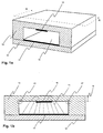
- FIGS 1a and 1b there is illustrated a possible alternative for realising an inverted microstrip cable based on the HTCC or LTCC multilayer technique according to the description above.
- the structure according to figure 1a is achieved by joining together, during the production process but prior to the burning step of the structure, the exemplary elements 12 and 13 illustrated in the drawing. Both of said elements are made layer by layer of some suitable dielectric material in a fashion described above.
- the element 13 there is machined a rectangular groove, on the bottom of which there is silk-screened a signal cable 10.
- the thickness 18 of the element 13, when measured at the bottom of the groove, is sufficient to prevent disturbing ground potential levels from coming close to the described inverted microstrip cable.
- the angle between the side walls of the groove made in the element 13 and the groove bottom 16, 17 is 90 degrees, but in principle the angles can have some other size, too.
- the elements 12 and 13 are machined separately, and when they are connected, there is obtained a structure according to figure 1a , where there is created a gas-filled cable cavity 14.
- FIG 1b there is illustrated a cross-section made in the direction A - A' of figure 1a .
- the attenuation and impedance of a transmission cable according to the invention are determined by the permittivity ( ⁇ r ) of the employed elements 12 and 13, as well as the geometric shape of the groove. From the drawing it is seen that the electromagnetic field emitted from the signal cable 10, said field in the drawing being illustrated by the power lines 15, proceeds a long way inside the element 13. With RF frequencies, the permittivity of the element 13 is clearly higher than the permittivity of the gas mixture filling the cable cavity 14. This results in that the cable attenuation is strongly increased with RF frequencies.
- the final multilayer structure of the apparatus also includes other material layers than those illustrated in figures 1a and 1b , in which layers there may be provided passive components, cavities for active components and other cable structures, too.
- the object of the invention is to reduce the described drawbacks connected to the prior art.
- the transmission cable placed in a cavity is characterised in that it comprises a support element with a surface essentially parallel to the first and second surfaces of the cavity, said support element being placed between said first and second surfaces, so that the signal cable is realised by means of an electroconductive material layer formed on the surface of said support element.
- the basic principle of the invention is as follows: by applying multilayer technique, there is manufactured a modified, inverted microstrip cable, where the signal cable is attached, by means of a specially designed support element, on one surface of the cable cavity.
- a specially designed support element on one surface of the cable cavity.
- An advantage of the invention is that at RF frequencies the attenuation of a transmission cable according to the invention is clearly lower than with existing inverted microstrip cables, because the electromagnetic field emitted from the signal cable is mainly located in the gas-filled cable cavity, the permittivity ( ⁇ r ) of said cable cavity with respect to the permittivity of the surrounding dielectric materials being low.
- Another advantage of the invention is that the transmission cable can be fully integrated in a multilayer structure without any specific work steps carried out expressly for this purpose.
- Yet another advantage of the invention is that thereby the impedance level of the transmission cable can be adjusted as desired in a simple fashion.
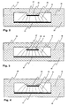
- Figures 2 - 6 represent a few preferred embodiments according to the invention. All embodiments illustrated in the drawings consist of elements manufactured by multilayer technique, which elements can in the manufacturing process be combined to form a uniform structure.
- the signal cable 20 of an inverted microstrip cable is attached to a support element 25 according to the invention.
- the walls surrounding the transmission cable can be made in a process explained above, in connection with the description of the prior art, for instance of two or more elements 22 and 23, which both are compiled of several green tapes.
- the sectional plane 26 of the elements, perpendicular to the patterns, is chosen so that the number of work steps in the manufacturing process is minimised.
- the support element 25 can likewise be made in several alternative ways. For example, it can be made so that the contact surface of the elements 22 and 23 is placed exactly on the level of the support element surface, which in the drawing is illustrated by a dotted line 26. On both sides of the support element 25, there are made grooves seen in the illustration.
- Another alternative is to make a groove in the element 23 according to the method described in connection with figure 1a and to manufacture the support element 25 and the signal cable 20 separately with respect to the sectional plane, starting from the sectional plane illustrated by the dotted line 27.
- the support element 25 and the signal cable 20 are in later manufacturing steps attached, as a uniform structure, on the bottom of the groove made in the element 23.
- the ground cable 21 is made either in the way described in connection with figure 1a , or it may be silk-screened in a groove of a suitable size provided in the element 22, if the contact surface of the elements 22 and 23 is the plane illustrated by the dotted line 26. When the elements 22, 23 and the support element 25 are connected, the ground cable 21 is placed in the cable cavity in parallel with the signal cable 20.
- the major part of the transmission cable losses are composed exactly of the losses made in the dielectric material layer.
- the inverted microstrip cable according to the invention has a smaller attenuation per unit of length than the inverted microstrip cable according to the prior art.
- the impedance level of the transmission cable according to the invention can be adjusted to the desired magnitude, because the impedance of the transmission cable is affected by adjusting the outer dimensions of the support element 25 made of some dielectric material.
- the signal cable 30 of an inverted microstrip cable is attached to a support element 35, which is narrowed in a triangular fashion towards the bottom of the transmission cable cavity.
- the cable structure according to the drawing is composed of at least two separate elements 32 and 33.
- the contact surface of the elements, which in the drawing is illustrated by the dotted line 36, is chosen to be the best possible with respect to the manufacturing of the structure.
- the contact surface 36 of the elements 32 and 33 can be, as is illustrated, the plane 30 of the signal cable attached to the support element 35, but it can also be some other plane.
- the support element 35 can be produced in connection with the production of the element 33, but it can also be produced separately, in which case its contact surface with the element 33 can be a plane which in the drawing is illustrated by the dotted line 37.
- Part of the electromagnetic field, illustrated by the power lines 34, emitted from the signal cable 30 towards the ground cable 31, proceeds for a short length inside the support element 35.
- the part of the electromagnetic field that is left inside the support element is smaller than the part left in the bottom substrate in the prior art arrangement illustrated in figure 1b .
- the attenuation per unit of length is thus lower than the attenuation of an inverted microstrip cable according to the prior art.
- the signal cable 40 of an inverted microstrip cable is attached to a support element 45 that is wider towards the bottom of the groove made in the element 43.
- the illustrated structure is composed of at least two separate elements 42 and 43. The elements are treated so that inside them, there is created a cable cavity according to the illustration.
- the contact surface of the elements 42 and 43, illustrated by the dotted line 46, is chosen to be the best possible with respect to the manufacturing of the product.
- the contact surface of the elements 42 and 43 can be, as is illustrated, a plane of the signal cable 40 attached to the support element 45, but it may also be another plane that is advantageous for the manufacturing process.
- the part that passes through the support element is remarkably smaller than in the case of the prior art inverted microstrip cable illustrated in figure 1b .
- the attenuation per unit of length also in this embodiment is lower than in a prior art inverted microstrip cable.
- the signal cable 50 of an inverted microstrip cable is attached to a support element 55 having the shape of a T-beam.
- the walls encasing the transmission cable are composed of at least two elements 52 and 53, and the sectional plane perpendicular to the patterns of said elements, said sectional plane being illustrated by the dotted line 56, is chosen so that the number of work steps in the manufacturing process is minimised.
- the support element 55 can be manufactured in several alternative ways. One alternative is to produce the support element 55 and the signal cable 50 separately, starting from the plane at the base of the T-beam, which plane is illustrated by the dotted line 57.
- the support element 55 and the signal cable 50 are connected, as a uniform structure, to the element 52.
- the ground cable 51 can be produced for instance in the way illustrated in connection with figure 1b .
- the ground cable 51 is located in the cable cavity on the opposite side of the signal cable 50.
- the inverted microstrip cable according to the drawing has an extremely low attenuation per length unit, in comparison with the attenuation of a prior art inverted microstrip cable.
- the transmission cable structure is composed of at least two elements 62 and 63.
- the contact surface of the elements 62 and 63, illustrated by the dotted line 66, is chosen to be the best possible with respect to the manufacturing of the product. It may be located at the illustrated point, in which case it is level with the surface of the support element 65, which in the drawing is illustrated by the dotted line 66.
- the shape of the support element is inwardly curved.
- the support element 65 constitutes part of the element 63.
- only a small part of the electric field emitted from the signal cable 60, which in figure 6 is illustrated by the power lines 64, proceeds in the dielectric material of the support element.
- the attenuation of an inverted microstrip cable according to the invention is low in comparison with a corresponding prior art transmission cable.
- the inverted microstrip cable according to the invention is placed in a cable cavity made of dielectric material layers.
- the number of the layers constituting the cable cavity wall may vary according to the employed technique and to an optimal number of working steps.
- the wall strength of the created cable cavity is assumed to be so good in all directions, that the other ground potential levels possibly located in the surroundings are placed far enough in order to prevent the shape of the electromagnetic field of the transmission cable from being disturbed thereby.
- the structure of the walls forming the cable cavity can be divided into various levels by innumerable different ways.
- the employed manufacturing technique determines which method of dividing the wall parts to be created is optimal with respect to expenses and output.
- the shape of the support element according to the invention can deviate from the preferred embodiments illustrated above.
- the manufacturing method of the employed signal and ground cables may be other than the suggested silk screen method.
- Other known cable structures, for example coplanar cable, can also be employed as the cable used in the structure.
- the inventive idea can be applied in various different ways within the scope of the patent claims.
Landscapes
- Microelectronics & Electronic Packaging (AREA)
- Engineering & Computer Science (AREA)
- Waveguides (AREA)
- Communication Cables (AREA)
- Optical Integrated Circuits (AREA)
- Insulated Conductors (AREA)
- Coils Or Transformers For Communication (AREA)
- Push-Button Switches (AREA)
- Electrotherapy Devices (AREA)
- Geophysics And Detection Of Objects (AREA)
- Transmitters (AREA)
- Particle Formation And Scattering Control In Inkjet Printers (AREA)
- Transducers For Ultrasonic Waves (AREA)
- Surface Acoustic Wave Elements And Circuit Networks Thereof (AREA)
- Semiconductor Integrated Circuits (AREA)
Applications Claiming Priority (3)
| Application Number | Priority Date | Filing Date | Title |
|---|---|---|---|
| FI990717A FI113580B (fi) | 1999-03-31 | 1999-03-31 | Invertoitu mikroliuska-siirtolinja monikerrosrakenteeseen integroituna |
| FI990717 | 1999-03-31 | ||
| PCT/FI2000/000274 WO2000062368A1 (en) | 1999-03-31 | 2000-03-30 | Inverted microstrip transmisson line integrated in a multilayer structure |
Publications (2)
| Publication Number | Publication Date |
|---|---|
| EP1166385A1 EP1166385A1 (en) | 2002-01-02 |
| EP1166385B1 true EP1166385B1 (en) | 2009-01-28 |
Family
ID=8554327
Family Applications (1)
| Application Number | Title | Priority Date | Filing Date |
|---|---|---|---|
| EP00917089A Expired - Lifetime EP1166385B1 (en) | 1999-03-31 | 2000-03-30 | Inverted microstrip transmisson line integrated in a multilayer structure |
Country Status (11)
| Country | Link |
|---|---|
| US (1) | US6714104B1 (ja) |
| EP (1) | EP1166385B1 (ja) |
| JP (1) | JP4170594B2 (ja) |
| CN (1) | CN1192452C (ja) |
| AT (1) | ATE422101T1 (ja) |
| AU (1) | AU758158B2 (ja) |
| BR (1) | BR0008596A (ja) |
| CA (1) | CA2367036C (ja) |
| DE (1) | DE60041484D1 (ja) |
| FI (1) | FI113580B (ja) |
| WO (1) | WO2000062368A1 (ja) |
Families Citing this family (5)
| Publication number | Priority date | Publication date | Assignee | Title |
|---|---|---|---|---|
| US5814702A (en) * | 1996-02-20 | 1998-09-29 | General Electric Company | Elastomer composition and thermoplastic resin composition modified therewith |
| US20050190019A1 (en) * | 2004-02-27 | 2005-09-01 | Carsten Metz | Low-loss transmission line structure |
| JP2009302606A (ja) * | 2008-06-10 | 2009-12-24 | Nippon Telegr & Teleph Corp <Ntt> | 伝送線路及び伝送線路の製造方法 |
| CN105514554A (zh) * | 2016-01-07 | 2016-04-20 | 北京同方吉兆科技有限公司 | 一种适用于大功率传输的倒置微带线结构 |
| KR20220096120A (ko) * | 2020-12-30 | 2022-07-07 | 삼성전자주식회사 | 삽입 손실을 줄이기 위한 전송 선로 구조 및 이를 포함하는 전자 장치 |
Citations (1)
| Publication number | Priority date | Publication date | Assignee | Title |
|---|---|---|---|---|
| WO2000038271A1 (en) * | 1998-12-22 | 2000-06-29 | Lk A/S | An electrical cable |
Family Cites Families (6)
| Publication number | Priority date | Publication date | Assignee | Title |
|---|---|---|---|---|
| US3904997A (en) * | 1973-09-13 | 1975-09-09 | Microwave Ass | Trapped-radiation microwave transmission line |
| US5105055A (en) | 1990-10-17 | 1992-04-14 | Digital Equipment Corporation | Tunnelled multiconductor system and method |
| JPH04368005A (ja) | 1991-06-14 | 1992-12-21 | Sanyo Electric Co Ltd | マイクロ波伝送線路 |
| WO1993002485A1 (en) | 1991-07-19 | 1993-02-04 | Fujitsu Limited | Microstrip line and manufacturing method therefor |
| JP2983169B2 (ja) | 1996-03-07 | 1999-11-29 | 株式会社移動体通信先端技術研究所 | 高周波用伝送線路の製造方法 |
| JP3218996B2 (ja) * | 1996-11-28 | 2001-10-15 | 松下電器産業株式会社 | ミリ波導波路 |
-
1999
- 1999-03-31 FI FI990717A patent/FI113580B/fi not_active IP Right Cessation
-
2000
- 2000-03-30 JP JP2000611335A patent/JP4170594B2/ja not_active Expired - Fee Related
- 2000-03-30 BR BR0008596-0A patent/BR0008596A/pt not_active IP Right Cessation
- 2000-03-30 US US09/937,506 patent/US6714104B1/en not_active Expired - Lifetime
- 2000-03-30 AT AT00917089T patent/ATE422101T1/de active
- 2000-03-30 AU AU38211/00A patent/AU758158B2/en not_active Ceased
- 2000-03-30 WO PCT/FI2000/000274 patent/WO2000062368A1/en active Search and Examination
- 2000-03-30 DE DE60041484T patent/DE60041484D1/de not_active Expired - Lifetime
- 2000-03-30 EP EP00917089A patent/EP1166385B1/en not_active Expired - Lifetime
- 2000-03-30 CA CA2367036A patent/CA2367036C/en not_active Expired - Lifetime
- 2000-03-30 CN CN00805866.0A patent/CN1192452C/zh not_active Expired - Fee Related
Patent Citations (1)
| Publication number | Priority date | Publication date | Assignee | Title |
|---|---|---|---|---|
| WO2000038271A1 (en) * | 1998-12-22 | 2000-06-29 | Lk A/S | An electrical cable |
Also Published As
| Publication number | Publication date |
|---|---|
| CN1346524A (zh) | 2002-04-24 |
| ATE422101T1 (de) | 2009-02-15 |
| WO2000062368A1 (en) | 2000-10-19 |
| CA2367036C (en) | 2010-06-29 |
| US6714104B1 (en) | 2004-03-30 |
| FI990717A0 (fi) | 1999-03-31 |
| BR0008596A (pt) | 2002-01-08 |
| AU758158B2 (en) | 2003-03-20 |
| EP1166385A1 (en) | 2002-01-02 |
| DE60041484D1 (de) | 2009-03-19 |
| CN1192452C (zh) | 2005-03-09 |
| CA2367036A1 (en) | 2000-10-19 |
| FI990717A (fi) | 2000-10-01 |
| FI113580B (fi) | 2004-05-14 |
| AU3821100A (en) | 2000-11-14 |
| JP4170594B2 (ja) | 2008-10-22 |
| JP2002542641A (ja) | 2002-12-10 |
Similar Documents
| Publication | Publication Date | Title |
|---|---|---|
| US11936111B2 (en) | Antenna array based on one or more metamaterial structures | |
| EP1196961B1 (en) | Method for creating waveguides in multilayer ceramic structures and a waveguide | |
| CN102696145B (zh) | 微带线和矩形波导间的微波转换设备 | |
| EP0883328B1 (en) | Circuit board comprising a high frequency transmission line | |
| US7750765B2 (en) | Compact via transmission line for printed circuit board and design method of the same | |
| JP5616338B2 (ja) | 平行な伝導表面間のギャップにおける導波管と伝送ライン | |
| JP2605654B2 (ja) | 複合マイクロ波回路モジュール及びその製造方法 | |
| JP3389819B2 (ja) | 誘電体導波管型共振器 | |
| US5499005A (en) | Transmission line device using stacked conductive layers | |
| WO1999027606A2 (en) | Microstrip arrangement | |
| JP2004112131A (ja) | 平面回路−導波管接続構造 | |
| WO2015124949A1 (en) | Ceramic waveguide filter apparatus | |
| EP1166385B1 (en) | Inverted microstrip transmisson line integrated in a multilayer structure | |
| DE69829327T2 (de) | Dielektrisches Filter, Sende/Empfangsweiche, und Kommunikationsgerät | |
| JPH10107518A (ja) | 誘電体導波管線路および配線基板 | |
| GB2222489A (en) | Waveguide apparatus | |
| US4647882A (en) | Miniature microwave guide | |
| GB2367952A (en) | Microwave dual mode dielectric resonator | |
| JP4080981B2 (ja) | 変換回路 | |
| KR20000022839A (ko) | 고주파 저손실 전극 | |
| JPH11136009A (ja) | 高周波用フレキシブル線路 | |
| CN1135657C (zh) | 具有多层接地面的快波振荡型天线 | |
| WO2023282042A1 (ja) | 電子部品 | |
| JP2000151225A (ja) | ストリップ線路−導波管変換装置 | |
| EP0357233A2 (en) | Waveguide apparatus |
Legal Events
| Date | Code | Title | Description |
|---|---|---|---|
| PUAI | Public reference made under article 153(3) epc to a published international application that has entered the european phase |
Free format text: ORIGINAL CODE: 0009012 |
|
| 17P | Request for examination filed |
Effective date: 20010918 |
|
| AK | Designated contracting states |
Kind code of ref document: A1 Designated state(s): AT BE CH CY DE DK ES FI FR GB GR IE IT LI LU MC NL PT SE |
|
| RAP1 | Party data changed (applicant data changed or rights of an application transferred) |
Owner name: NOKIA CORPORATION |
|
| GRAP | Despatch of communication of intention to grant a patent |
Free format text: ORIGINAL CODE: EPIDOSNIGR1 |
|
| GRAS | Grant fee paid |
Free format text: ORIGINAL CODE: EPIDOSNIGR3 |
|
| GRAA | (expected) grant |
Free format text: ORIGINAL CODE: 0009210 |
|
| AK | Designated contracting states |
Kind code of ref document: B1 Designated state(s): AT BE CH CY DE DK ES FI FR GB GR IE IT LI LU MC NL PT SE |
|
| REG | Reference to a national code |
Ref country code: GB Ref legal event code: FG4D |
|
| REG | Reference to a national code |
Ref country code: CH Ref legal event code: EP Ref country code: CH Ref legal event code: NV Representative=s name: CABINET MOUTARD |
|
| REG | Reference to a national code |
Ref country code: IE Ref legal event code: FG4D |
|
| REF | Corresponds to: |
Ref document number: 60041484 Country of ref document: DE Date of ref document: 20090319 Kind code of ref document: P |
|
| NLV1 | Nl: lapsed or annulled due to failure to fulfill the requirements of art. 29p and 29m of the patents act | ||
| PG25 | Lapsed in a contracting state [announced via postgrant information from national office to epo] |
Ref country code: ES Free format text: LAPSE BECAUSE OF FAILURE TO SUBMIT A TRANSLATION OF THE DESCRIPTION OR TO PAY THE FEE WITHIN THE PRESCRIBED TIME-LIMIT Effective date: 20090509 Ref country code: NL Free format text: LAPSE BECAUSE OF FAILURE TO SUBMIT A TRANSLATION OF THE DESCRIPTION OR TO PAY THE FEE WITHIN THE PRESCRIBED TIME-LIMIT Effective date: 20090128 Ref country code: FI Free format text: LAPSE BECAUSE OF FAILURE TO SUBMIT A TRANSLATION OF THE DESCRIPTION OR TO PAY THE FEE WITHIN THE PRESCRIBED TIME-LIMIT Effective date: 20090128 |
|
| PG25 | Lapsed in a contracting state [announced via postgrant information from national office to epo] |
Ref country code: SE Free format text: LAPSE BECAUSE OF FAILURE TO SUBMIT A TRANSLATION OF THE DESCRIPTION OR TO PAY THE FEE WITHIN THE PRESCRIBED TIME-LIMIT Effective date: 20090428 Ref country code: PT Free format text: LAPSE BECAUSE OF FAILURE TO SUBMIT A TRANSLATION OF THE DESCRIPTION OR TO PAY THE FEE WITHIN THE PRESCRIBED TIME-LIMIT Effective date: 20090629 |
|
| PG25 | Lapsed in a contracting state [announced via postgrant information from national office to epo] |
Ref country code: DK Free format text: LAPSE BECAUSE OF FAILURE TO SUBMIT A TRANSLATION OF THE DESCRIPTION OR TO PAY THE FEE WITHIN THE PRESCRIBED TIME-LIMIT Effective date: 20090128 Ref country code: MC Free format text: LAPSE BECAUSE OF NON-PAYMENT OF DUE FEES Effective date: 20090331 |
|
| PLBE | No opposition filed within time limit |
Free format text: ORIGINAL CODE: 0009261 |
|
| STAA | Information on the status of an ep patent application or granted ep patent |
Free format text: STATUS: NO OPPOSITION FILED WITHIN TIME LIMIT |
|
| 26N | No opposition filed |
Effective date: 20091029 |
|
| PG25 | Lapsed in a contracting state [announced via postgrant information from national office to epo] |
Ref country code: IE Free format text: LAPSE BECAUSE OF NON-PAYMENT OF DUE FEES Effective date: 20090330 |
|
| PG25 | Lapsed in a contracting state [announced via postgrant information from national office to epo] |
Ref country code: GR Free format text: LAPSE BECAUSE OF FAILURE TO SUBMIT A TRANSLATION OF THE DESCRIPTION OR TO PAY THE FEE WITHIN THE PRESCRIBED TIME-LIMIT Effective date: 20090429 |
|
| PG25 | Lapsed in a contracting state [announced via postgrant information from national office to epo] |
Ref country code: IT Free format text: LAPSE BECAUSE OF FAILURE TO SUBMIT A TRANSLATION OF THE DESCRIPTION OR TO PAY THE FEE WITHIN THE PRESCRIBED TIME-LIMIT Effective date: 20090128 |
|
| PG25 | Lapsed in a contracting state [announced via postgrant information from national office to epo] |
Ref country code: LU Free format text: LAPSE BECAUSE OF NON-PAYMENT OF DUE FEES Effective date: 20090330 |
|
| PG25 | Lapsed in a contracting state [announced via postgrant information from national office to epo] |
Ref country code: CY Free format text: LAPSE BECAUSE OF FAILURE TO SUBMIT A TRANSLATION OF THE DESCRIPTION OR TO PAY THE FEE WITHIN THE PRESCRIBED TIME-LIMIT Effective date: 20090128 |
|
| REG | Reference to a national code |
Ref country code: CH Ref legal event code: PFA Owner name: NOKIA CORPORATION Free format text: NOKIA CORPORATION#KEILALAHDENTIE 4#02150 ESPOO (FI) -TRANSFER TO- NOKIA CORPORATION#KEILALAHDENTIE 4#02150 ESPOO (FI) |
|
| REG | Reference to a national code |
Ref country code: CH Ref legal event code: PCAR Free format text: NEW ADDRESS: RUE DE LYON 75 - 4EME ETAGE, 1203 GENEVE (CH) |
|
| REG | Reference to a national code |
Ref country code: GB Ref legal event code: 732E Free format text: REGISTERED BETWEEN 20150910 AND 20150916 |
|
| REG | Reference to a national code |
Ref country code: DE Ref legal event code: R081 Ref document number: 60041484 Country of ref document: DE Owner name: NOKIA TECHNOLOGIES OY, FI Free format text: FORMER OWNER: NOKIA CORP., 02610 ESPOO, FI |
|
| REG | Reference to a national code |
Ref country code: CH Ref legal event code: PUE Owner name: NOKIA TECHNOLOGIES OY, FI Free format text: FORMER OWNER: NOKIA CORPORATION, FI |
|
| REG | Reference to a national code |
Ref country code: FR Ref legal event code: PLFP Year of fee payment: 17 |
|
| REG | Reference to a national code |
Ref country code: AT Ref legal event code: PC Ref document number: 422101 Country of ref document: AT Kind code of ref document: T Owner name: NOKIA TECHNOLOGIES OY, FI Effective date: 20160104 |
|
| PGFP | Annual fee paid to national office [announced via postgrant information from national office to epo] |
Ref country code: CH Payment date: 20160311 Year of fee payment: 17 |
|
| PGFP | Annual fee paid to national office [announced via postgrant information from national office to epo] |
Ref country code: BE Payment date: 20160215 Year of fee payment: 17 Ref country code: AT Payment date: 20160225 Year of fee payment: 17 |
|
| REG | Reference to a national code |
Ref country code: FR Ref legal event code: TP Owner name: NOKIA TECHNOLOGIES OY, FI Effective date: 20170109 |
|
| REG | Reference to a national code |
Ref country code: FR Ref legal event code: PLFP Year of fee payment: 18 |
|
| REG | Reference to a national code |
Ref country code: CH Ref legal event code: PL |
|
| REG | Reference to a national code |
Ref country code: AT Ref legal event code: MM01 Ref document number: 422101 Country of ref document: AT Kind code of ref document: T Effective date: 20170330 |
|
| PG25 | Lapsed in a contracting state [announced via postgrant information from national office to epo] |
Ref country code: AT Free format text: LAPSE BECAUSE OF NON-PAYMENT OF DUE FEES Effective date: 20170330 |
|
| PG25 | Lapsed in a contracting state [announced via postgrant information from national office to epo] |
Ref country code: LI Free format text: LAPSE BECAUSE OF NON-PAYMENT OF DUE FEES Effective date: 20170331 Ref country code: CH Free format text: LAPSE BECAUSE OF NON-PAYMENT OF DUE FEES Effective date: 20170331 |
|
| REG | Reference to a national code |
Ref country code: BE Ref legal event code: MM Effective date: 20170331 Ref country code: BE Ref legal event code: PD Owner name: NOKIA TECHNOLOGIES OY; FI Free format text: DETAILS ASSIGNMENT: CHANGE OF OWNER(S), AFFECTATION / CESSION; FORMER OWNER NAME: NOKIA CORPORATION Effective date: 20151117 |
|
| REG | Reference to a national code |
Ref country code: FR Ref legal event code: PLFP Year of fee payment: 19 |
|
| PGFP | Annual fee paid to national office [announced via postgrant information from national office to epo] |
Ref country code: GB Payment date: 20180321 Year of fee payment: 19 Ref country code: DE Payment date: 20180322 Year of fee payment: 19 |
|
| PG25 | Lapsed in a contracting state [announced via postgrant information from national office to epo] |
Ref country code: BE Free format text: LAPSE BECAUSE OF NON-PAYMENT OF DUE FEES Effective date: 20170331 |
|
| PGFP | Annual fee paid to national office [announced via postgrant information from national office to epo] |
Ref country code: FR Payment date: 20180323 Year of fee payment: 19 |
|
| REG | Reference to a national code |
Ref country code: GB Ref legal event code: 732E Free format text: REGISTERED BETWEEN 20190124 AND 20190130 |
|
| REG | Reference to a national code |
Ref country code: DE Ref legal event code: R081 Ref document number: 60041484 Country of ref document: DE Owner name: PROVENANCE ASSET GROUP LLC, PITTSFORD, US Free format text: FORMER OWNER: NOKIA TECHNOLOGIES OY, ESPOO, FI |
|
| REG | Reference to a national code |
Ref country code: DE Ref legal event code: R119 Ref document number: 60041484 Country of ref document: DE |
|
| GBPC | Gb: european patent ceased through non-payment of renewal fee |
Effective date: 20190330 |
|
| PG25 | Lapsed in a contracting state [announced via postgrant information from national office to epo] |
Ref country code: DE Free format text: LAPSE BECAUSE OF NON-PAYMENT OF DUE FEES Effective date: 20191001 Ref country code: GB Free format text: LAPSE BECAUSE OF NON-PAYMENT OF DUE FEES Effective date: 20190330 |
|
| PG25 | Lapsed in a contracting state [announced via postgrant information from national office to epo] |
Ref country code: FR Free format text: LAPSE BECAUSE OF NON-PAYMENT OF DUE FEES Effective date: 20190331 |