EP1162507A2 - Alignment method, overlay deviation inspection method and photomask - Google Patents
Alignment method, overlay deviation inspection method and photomask Download PDFInfo
- Publication number
- EP1162507A2 EP1162507A2 EP01112985A EP01112985A EP1162507A2 EP 1162507 A2 EP1162507 A2 EP 1162507A2 EP 01112985 A EP01112985 A EP 01112985A EP 01112985 A EP01112985 A EP 01112985A EP 1162507 A2 EP1162507 A2 EP 1162507A2
- Authority
- EP
- European Patent Office
- Prior art keywords
- mark
- photomask
- deviation
- inspection
- pattern
- Prior art date
- Legal status (The legal status is an assumption and is not a legal conclusion. Google has not performed a legal analysis and makes no representation as to the accuracy of the status listed.)
- Granted
Links
Images




Classifications
-
- H—ELECTRICITY
- H10—SEMICONDUCTOR DEVICES; ELECTRIC SOLID-STATE DEVICES NOT OTHERWISE PROVIDED FOR
- H10P—GENERIC PROCESSES OR APPARATUS FOR THE MANUFACTURE OR TREATMENT OF DEVICES COVERED BY CLASS H10
- H10P76/00—Manufacture or treatment of masks on semiconductor bodies, e.g. by lithography or photolithography
-
- G—PHYSICS
- G03—PHOTOGRAPHY; CINEMATOGRAPHY; ANALOGOUS TECHNIQUES USING WAVES OTHER THAN OPTICAL WAVES; ELECTROGRAPHY; HOLOGRAPHY
- G03F—PHOTOMECHANICAL PRODUCTION OF TEXTURED OR PATTERNED SURFACES, e.g. FOR PRINTING, FOR PROCESSING OF SEMICONDUCTOR DEVICES; MATERIALS THEREFOR; ORIGINALS THEREFOR; APPARATUS SPECIALLY ADAPTED THEREFOR
- G03F7/00—Photomechanical, e.g. photolithographic, production of textured or patterned surfaces, e.g. printing surfaces; Materials therefor, e.g. comprising photoresists; Apparatus specially adapted therefor
- G03F7/70—Microphotolithographic exposure; Apparatus therefor
- G03F7/70483—Information management; Active and passive control; Testing; Wafer monitoring, e.g. pattern monitoring
- G03F7/70605—Workpiece metrology
- G03F7/70616—Monitoring the printed patterns
- G03F7/70633—Overlay, i.e. relative alignment between patterns printed by separate exposures in different layers, or in the same layer in multiple exposures or stitching
-
- G—PHYSICS
- G03—PHOTOGRAPHY; CINEMATOGRAPHY; ANALOGOUS TECHNIQUES USING WAVES OTHER THAN OPTICAL WAVES; ELECTROGRAPHY; HOLOGRAPHY
- G03F—PHOTOMECHANICAL PRODUCTION OF TEXTURED OR PATTERNED SURFACES, e.g. FOR PRINTING, FOR PROCESSING OF SEMICONDUCTOR DEVICES; MATERIALS THEREFOR; ORIGINALS THEREFOR; APPARATUS SPECIALLY ADAPTED THEREFOR
- G03F9/00—Registration or positioning of originals, masks, frames, photographic sheets or textured or patterned surfaces, e.g. automatically
- G03F9/70—Registration or positioning of originals, masks, frames, photographic sheets or textured or patterned surfaces, e.g. automatically for microlithography
- G03F9/7073—Alignment marks and their environment
- G03F9/7076—Mark details, e.g. phase grating mark, temporary mark
-
- H—ELECTRICITY
- H10—SEMICONDUCTOR DEVICES; ELECTRIC SOLID-STATE DEVICES NOT OTHERWISE PROVIDED FOR
- H10W—GENERIC PACKAGES, INTERCONNECTIONS, CONNECTORS OR OTHER CONSTRUCTIONAL DETAILS OF DEVICES COVERED BY CLASS H10
- H10W46/00—Marks applied to devices, e.g. for alignment or identification
- H10W46/501—Marks applied to devices, e.g. for alignment or identification for use before dicing
Definitions
- the present invention relates to an alignment method for precisely overlaying photomasks used in lithography steps performed in manufacturing of semiconductor devices, a pattern-overlay inspection method, and a photomask used in these methods.
- a semiconductor wafer is exposed to lights having mask patterns exceeding 20 patterns to overlay the mask patterns successively on the semiconductor wafer for forming finally a plurality of device patterns on the semiconductor wafer.
- the pattern exposure is performed, the positioning of a photomask in an exposure apparatus is performed according to an alignment mark formed in advance on the photomask. After the positioning is fixed, the pattern exposure is performed to form a resist pattern on a chip of the semiconductor wafer for correctly overlaying the resist pattern on a pattern formed in advance within the chip.
- the pattern-overlay inspection is then performed on the basis of the resist pattern and the pattern formed in advance on the chip so as to inspect whether a device pattern to be formed is correctly overlaid on the device pattern formed in advance on the chip.
- FIG. 8 is a plan view showing typical conventional inspection marks for inspecting the deviation of alignment formed on the wafer together with a device pattern.
- the inspection marks include inner four marks 101 and outer four marks 102.
- the outer marks 102 are arranged to have a pitch of 28 ⁇ m as shown in the figure. Therefore, each of the outer marks 102 has a length slightly shorter than 28 ⁇ m.
- the inspection marks 101 are formed in advance in the first layer of wires on the wafer, for example, and the inspection marks 102 are then formed on a second layer of wires on the first layer of wires to have an arrangement as shown in FIG. 8.
- the deviation of alignment can be inspected by obtaining a subtraction of a measured distance between the neighboring marks 101 and 102 and a reference distance, for example.
- the difficulty is derived from the situation that the inspection marks for inspecting the deviation of alignment and the device pattern are not similar or equal to each other in size and shape.
- an error in the pattern position, size and shape takes place due to the aberration and focus position of the projection optical system including a projection lens in the exposure apparatus used in the lithography.
- the degree of the error varies depending on the shape, size and local density of the inspection marks and those of the device patterns.
- FIG. 9 exemplifies a device pattern formed on the wafer together with the overlay deviation inspection marks shown in FIG. 8, for example. As shown in FIG. 9, the pitch of the device pattern is 0.35 ⁇ m. Thus, the device pattern shown in FIG. 9 is utterly different from the inspection marks shown in FIG. 8 in shape and size.
- the device pattern includes in some cases patterns differing from each other in the shape, size, density, etc. even if these patterns are formed on the same layer of wires on the wafer. In such a case, a difference in the error amount in respect of the pattern position and shape takes place depending on the difference in the pattern size and shape. In order to form a precise pattern, it is desirable to measure the errors in the position, shape and size of all the device patterns. However, such a measuring means has not been developed in the past.
- the similar problems are also generated in the alignment mark used for finding the alignment position of the photo-mask in the light exposure step performed by using the exposure apparatus as well as in the inspection mark for measuring the deviation of alignment.
- a difficulty is generated that it is difficult to recognize correctly the actual device pattern position on the wafer exposed to the light.
- FIG. 10 is a plan view showing the conventional alignment mark formed on a wafer.
- the conventional alignment mark has a pattern having a pitch of 12 ⁇ m larger than that of the device pattern shown in FIG. 9 and is shaped like an oblong band, which widely differs from the device pattern shown in FIG. 9 in shape, size, etc.
- Jpn. Pat. Appln. KOKAI No. 9-102457 discloses a means for solving the problem of an error generated from the situation that the alignment mark differs from the device pattern in shape and size. It is disclosed that the length of the alignment mark is divided into a length close to that of the device pattern. However, since the mark for inspecting the deviation of alignment and the alignment mark are designed separately from each other in the past, the inspecting mark and the alignment mark widely differ from each other in, for example, the pitch as apparent from FIGS. 8 and 10, resulting in failure to permit these inspecting mark and the alignment mark to be related to each other in the pattern size and shape.
- the alignment mark, the mark for inspecting the deviation of alignment, and the device pattern differ from each other in the constituents of the pattern such as the pattern shape, size and density, with the result that the degrees of errors taking place in the pattern forming step differ from each other.
- the alignment mark, the mark for inspecting the deviation of alignment, and the device pattern differ from each other in the constituents of the pattern such as the pattern shape, size and density, with the result that the degrees of errors taking place in the pattern forming step differ from each other.
- An object of the present invention is to provide an alignment method, a high accuracy overlay inspection method and a photomask used in these methods, in which both the alignment mark and the device pattern are formed so as to be affected in substantially the same degree by the error caused by the aberration of the projection optical system of the light exposure device used in exposing the pattern to the exposure light and by the error in the processing.
- the amount of the positional deviation of the device pattern is rendered substantially equal to the amount of the positional deviation of the alignment mark and the mark for inspecting the overlay of photomasks.
- an alignment method that is expected to achieve the alignment with a high accuracy, an inspecting method of overlay of device patterns in a high accuracy, and a photomask used for these methods.
- the present invention is featured in that, where a first photomask and a second photomask are used in the lithography step employed in the manufacturing process of a semiconductor device, the mark for inspecting the deviation of the alignment of the mask and the alignment mark are constructed to include at least a part of the device pattern included in these masks when the first or second photomask is used for the light exposure. Since each of the alignment mark and the mark for inspecting the overlay of device pattern includes a mark equal or similar to those of the device pattern in size and shape in the corresponding photomask, the error caused by the aberration of the projection optical system used in the pattern exposure step and the error in the processing are received in substantially the same amount. As a result, the amounts of the positional deviation of these marks and patterns are substantially the same so as to make it possible to expect an alignment of a high accuracy.
- the present invention is also featured in that, where a first photomask and a second photomask are used in the lithography step included in the manufacturing process of a semiconductor device, marks capable of measuring the relative deviation amount taking place among different patterns in size and shape are formed in the first photomask as the marks for the overlay inspection of the device patterns.
- the marks capable of measuring the relative deviation amount among the different patterns include a reference pattern having a relatively small deviation with respect to that of the device pattern shape and a mark having a relatively large deviation with respect to the device pattern shape.
- the second photomask has also overlay inspection marks capable of measuring the amount of the relative deviation among different patterns, the relative deviation taking place when the second photomask is used for the light exposure.
- the marks include a reference mark having a relatively small deviation with respect to that of the device pattern shape and a mark having a relatively large deviation with respect to the device pattern shape, in the same manner as the first photomask.
- the positionsal deviation of the first photomask and the second photomask Since the amounts of the positional deviation of the first photomask and the second photomask, the positional deviation being caused by the aberration of the projection optical system of the device pattern, are measured, and the result of the measurement is used for correcting the position in performing the light exposure by using the first photomask and the second photomask which are overlaid one upon the other, it is possible to expect the alignment of a high accuracy.
- the present invention is featured in that, where a first photomask and a second photomask are used in the lithography step included in the manufacturing process of a semiconductor device, the reference patterns of the first and second masks are the patterns receiving substantially the same error even if there is an error in the aberration of the projection optical system.
- the overlay is corrected in view of the error in the relative positional deviation of the device shape relative to the reference pattern of the first photomask and in view of the similar error of the second photomask, making it possible to obtain a desired overlaying accuracy.
- the mark for inspecting the deviation of overlay and the alignment mark included in each of these photomasks are constructed to include at least a part of the device pattern shape included in the mask.
- FIGS. 1A to 1C schematically show the state that, when a device pattern portion 4 of FIG. 1B is formed on a chip 11 by exposing a wafer 1 to light by using first and second photomasks, an alignment mark and an inspecting mark are formed simultaneously, and that these marks and the device pattern are formed on the chip 11 in positions deviated by predetermined amounts from an ideal positions.
- the device pattern portion 4 is formed by using a first photomask 21 in a predetermined position on each of a plurality of chips 11 formed on the wafer 1 shown in, for example, FIG. 7, e.g., in the position shown in FIG. 1B together with an alignment mark portion 25B and a mark portion 5B for inspecting the deviation of overlay.
- a mask pattern 25A consisting of a mask substrate 23 of a glass plate and a light shielding film 24 of a predetermined pattern formed on the mask substrate 23 is formed on the photomask 21, as shown in FIG. 1A.
- Light emitted from a light source (not shown) is incident on the first photomask 21 from the upper surface of the mask substrate 23 and passes through the light shielding film 24 so as to form a patterned light of the alignment mark.
- the patterned light is converged by a projection lens 3 so as to be projected as an alignment mark 41 within the alignment mark portion 25B on a resist film 21A formed on the wafer 1.
- an ideal pattern forming position when the positional deviation amount of the mask pattern 25A is zero, is denoted by broken lines, the alignment mark 41 exposed to light is deviated in the X-direction in an amount of X1.
- the alignment mark 25A within the alignment mark portion 25B on the first photomask 21 is affected by, for example, the aberration of the projection lens 3, with the result that the alignment mark 25A is formed as a transferred alignment mark 41 in a position deviated from the desired position in an amount of X1 as shown by the solid line in FIG. 1A.
- the alignment mark 41 is formed on the wafer 1 by using a resist mask formed by developing the resist 21A that was exposed to light, the alignment mark 41 is formed in a position deviated from the position of the alignment mark 25A on the photomask 21 in an amount of X1.
- the resist 21A is exposed to light by using an inspecting mark 5A within the inspecting mark portion 5B formed on the first photomask 21, as shown in the left portion of FIG. 1A.
- the inspecting mark 5A is also affected by, for example, the aberration of the projection lens 3, with the result that the inspecting mark 5A is formed as a mark portion 42 for inspecting the deviation of the transfer alignment in a position deviated from the ideal position denoted by broken lines in an amount of X1.
- the inspecting mark 42 is formed as the mark portion 41 for inspecting the deviation in a position deviated in an amount of X1 from the ideal mark 5A formed on the photomask 21 for inspecting the deviation of overlay, as shown in FIG. 1A. Therefore, the relative positions between the alignment mark 41 or the overlay inspection mark 42 and the device pattern on the chip 11 are similar to those on the photomask 21.
- the positional deviation in the X-direction alone is shown in FIG. 1A.
- the positional deviation caused by, for example, the aberration of the projection lens 3 takes place not only in the X-direction but also in the Y-direction.
- the positional deviation in the X-direction alone is described herein. Needless to say, however, it is necessary to inspect the amount of the positional deviation and to correct the deviation in the Y-direction, too. Since the position deviation in the Y-direction can be corrected as in the correction of the positional deviation in the X-direction, description is omitted herein in respect of the correction of the positional deviation in the Y-direction.
- a resist 22A newly formed on the wafer 1 by using a second photomask 22 formed of a glass substrate 26 and a light shielding film 27 formed on the substrate 26 is exposed to light, as shown in FIG. 1B.
- Formed on the second photomask 22 are a mark for inspecting the deviation of overlay together with the device pattern. An alignment mark is not formed on the second photomask 22.
- the mark for inspecting the deviation of alignment formed on the second photomask 22 is a mark 43 for inspecting the deviation of alignment formed inside the mark 42, as shown in FIG. 1C, unlike the mark 42 for inspecting the deviation of alignment, which is formed on the chip 11 by using the mask mark 5A for inspecting the deviation of alignment, which is formed on the first photomask 21.
- the mark 43 differs in size and shape from those of the mark 42 so as to distinguish easily these marks 42 and 43. Also, the mark 43 for inspecting the deviation of alignment is formed on the wafer at a position different from that of the mark 42. In this embodiment, the mark 43 is formed inside the mark 42. However, the mark 43 may be formed outside the mark 42.
- the exposure position of the second photomask 22 is adjusted in conformity with the alignment mark 41 within the alignment mark portion 25B within the chip 11 on the wafer 1 in the step of exposing the resist film 22A to light by using a light exposure apparatus. Therefore, the second photomask 22 does not require a mask pattern for the alignment mark. However, when another alignment mark is required for alignment a third photomask, for example, this another alignment mark may be formed on the chip 11 aligned to the alignment mark formed on the chip 11 using the second photomask 22.
- the mark 43 for inspecting the deviation of alignment which is transferred to the chip 11 on the wafer 1 by using the second photomask 22, is transferred inside the mark 42 for inspecting the deviation of alignment, which is transferred by using the first photomask 21.
- Each of the alignment mark 25A of the first photomask and the mark 5A for inspecting the deviation of alignment uses at least a part of the device pattern of the first photomask 21 as it is, or use a pattern equal to or similar to the device pattern. Also, the mark 43 for inspecting the deviation of alignment of the second photomask 22 is substantially equal in size and shape to the device pattern (not shown) of the second photomask 22.
- the device pattern and the overlay inspection mark 43 formed on the chip 11 using the second photomask 22 are affected in the similar degree by the aberration and focus position of the projection lens 3 and the deviation of the device pattern is similar to the overlay inspection mark 43.
- the deviation of the device pattern and the marks of the first photomask 21 formed on the chip 11 and the deviation of the device pattern and the marks of the second photomask 22 formed on the chip 11 are not the same, because the sizes and shapes of the first and second photomasks are not the same and because the deviation is also affected by the mechanical errors of the exposure apparatus and a change in the exposure conditions when the first and second photomasks are used in the same exposure apparatus.
- the deviation amount of the mark 43 from the center of the mark 42 will show the difference of the deviation of the marks caused by the difference of the sizes and shapes of the device patterns on the first and second photomasks 21 and 22, as shown in FIG. 1C.
- the deviation of alignment between the result of light exposure of the first photomask 21 and the result of light exposure of the second photomask 22 is measured by using a mark for measuring the deviation of alignment consisting of the first mark 42 for inspecting the deviation of alignment formed on the chip 11 and the mark 43 for inspecting the deviation of alignment formed on the resist 22A.
- the deviation of alignment noted above can be measured by forming each of the marks 42 and 43 on the chip 11.
- the difference D between the center C1 of the center points G1 and G2 in the outer overlay inspection marks 42 and the center C2 of the center points G3 and G4 in the inner overlay inspection marks 43 is measured.
- This measured difference D shows a deviation generated between the overlay inspection marks formed on the chip 11 by using the photomasks 21 and 22.
- the mark 42 for inspecting the deviation of alignment is a mark formed by the light exposure of the first photomask 21 and has a shape equal to or similar to a part of the device pattern 4 included in the first photomask 21.
- the mark 43 for inspecting the deviation of alignment is a mark formed by the light exposure of the second photomask 22 and has a shape equal to or similar to a part of the device pattern (not shown) included in the second photomask 22.
- the mark 43 for inspecting the deviation of overlay is shown in a large shape differing from the actual shape for the sake of convenience in the drawing. In general, however, the mark 43 is divided like the mark 42 for inspecting the deviation of alignment, though it is possible for the marks 42 and 43 to be slightly different from each other in the shape.
- the mark consist of the mark 102 for inspecting the deviation of overlay, which is formed by using the first photomask 21, and the mark 101 for inspecting the deviation of overlay, which is formed by using the second photomask 22.
- each of the alignment mark 41 and the marks 42, 43 for inspecting the deviation of overlay includes a part or a similar pattern of the device pattern, with the result that these marks receive the error caused by the influence of the aberration of the projection optical system such as a projection lens used in performing the pattern transfer in substantially the same degree.
- the projection optical system such as a projection lens used in performing the pattern transfer in substantially the same degree.
- FIGS. 2A to 2D collectively show schematically the alignment mark and the mark for inspecting the deviation of overlay, in a case in which are formed different patterns on the same photomask.
- the second embodiment is featured in that, in the case where a first photomask and a second photomask are used in the lithography step included in the manufacturing process of a semiconductor device, and the light exposure is performed by using the first or second photomask, each of the mark for inspecting the deviation of overlay of the device patterns and the alignment mark includes at least a part of the device pattern shape included in the photomasks.
- the first photomask includes first and second device patterns having different sizes and shapes and the second photomask includes a third device pattern of a size and shape different from those of the first and second device patterns. Therefore, the first and second photomasks include the overlay inspection mark and an alignment mark each having at least a part of these first to third device patterns.
- each of the alignment mark and the mark for inspecting the deviation of overlay is formed by combining different patterns on the same photomask.
- the patterns are selected from the typical patterns within the device patterns included in the first and second photomasks.
- a thick pattern and a fine pattern are selected from the device pattern in order to facilitate the description of the present invention. These thick pattern and fine pattern are alternately arranged in the patterns of the alignment mark and the mark for inspecting the deviation of overlay.
- the thick pattern and the fine pattern differ from each other in the amount of generation of the positional error when these patterns are transferred onto the wafer. It is possible to measure the positions of the thick pattern and the fine pattern by subjecting the generation amount of the positional error to a signal processing.
- an alignment mark consisting of a thick pattern 32 and a thin pattern 33 alternately arranged is formed in a first photomask 31.
- the alignment mark is transferred onto a wafer 30 by using these thick pattern and fine pattern.
- the fine pattern 33 in a position that should originally be transferred is actually deviated in its position so as to actually allow a fine pattern 34 to be transferred in a deviated position.
- the rate of the positional deviation of the fine pattern 33 is larger than that of the thick pattern 32.
- each of the position of the thick pattern 32 and the position of the fine pattern 33 is measured by a signal processing in view of the difference in the generation amount of the positional error noted above.
- the ideal position of the fine pattern 33 shown by the dotted lines is deviated at the position shown by the solid lines as the deviated fine pattern 34.
- the degree of the deviation of the fine pattern 34 is larger than that of the thick pattern 32. In this case, the deviation of the thick pattern 32 is assumed to be substantially zero.
- the deviation of the thick pattern 32 is not zero and is deviated slightly in X and Y directions. Therefore, when a distance between the transferred thick pattern 32 and the transferred thin pattern 34 is measured, the measured distance will denote a sum of an original distance between the thick and thin patterns on the photomask 31 and a difference between the deviation of the thick pattern and the deviation of the thin pattern transferred on the wafer, or a relative deviation amount therebetween. Therefore, when the original distance is subtracted from the sum value, the resultant value will denote a relative deviation amount ⁇ X in the X direction. In this manner, the positional deviation amount ⁇ X due to the pattern difference of the device patterns can be determined on the alignment mark transferred on the wafer.
- the relative deviation amount between alignment marks corresponding to the thick pattern 32d and thin pattern 33d which are included in the device pattern in the first photomask is measured by processing measured signals by taking the amount ⁇ X into consideration.
- a pattern 39d corresponding to a device pattern is transferred between the thick pattern 32 and the thin pattern 33 having an intermediate size between those of the thick and thin patterns 32 and 33 on the wafer using the second photomask.
- the relative deviation amounts ⁇ X of the thick and thin patterns 32 and 33 are known, it is easy to align the second photomask so as to position the third pattern 39d at the center position between the thick and thin patterns 32 and 33.
- FIGS. 2B and 2C show another case in which a third pattern 39d is first formed on the wafer using the first photomask and then the overlay inspection marks used to transfer the thick pattern 32d and thin pattern 33d are formed in such a manner that the third pattern 39d is positioned at the center of the thick and thin patterns 32d and 33d, as shown in FIG. 2D.
- the overlay inspection marks in the case where the device patterns have thick patterns, or the marks for inspecting the deviation of overlay for a large pattern comprising reference patterns 35 and 37 are formed on the wafer using the first photomask 31.
- the third pattern 39d having the intermediate size is formed as shown in FIG. 2D.
- another thick pattern 36 is formed as the overlay inspection mark inside the thick patterns 35 by the second photomask.
- the third pattern 39d is designed to be formed at an intermediate position of the thick and thin patterns 32d and 33d as shown in FIG. 2D.
- the mark for inspecting the deviation of alignment for a small pattern comprises a thick pattern 37 formed of the first photomask and a fine pattern 38 formed of the second photomask.
- the overlay error in the case where the device pattern has a thick pattern can be measured using the overlay inspection marks 35 and 36 shown in FIG. 2B, and the overlay error in the case of thin device pattern can be measured using the overlay inspection marks 37 and 38 shown in FIG. 2C.
- the overlay inspection for the respective device patterns can be performed. Therefore, as shown in FIG. 2D, it is easy to form the thick pattern 32d and the thin pattern 33d using the second photomask with respect to the device pattern 39d of the intermediate size using the first photomask at a correct position.
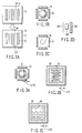
- FIGS. 3A to 3C collectively show schematically the marks for inspecting the deviation of alignment each formed on the photomask.
- first and second sets of overlay inspection marks are formed using the first and second photomasks.
- the first set of overlay inspection marks are prepared for measuring a first error denoting mainly a mechanical error caused by the exposure apparatus, which does not include an error due to the aberration of the projection lens.
- the second set of overlay inspection marks are prepared for measuring a second error mainly caused by the exposure error due to the projection lens.
- the overlay of the second photomask is adjusted by taking the first and second errors into consideration, thereby achieving a desired accuracy of the pattern overlay.
- an alignment mark equal to that used in the first embodiment shown in FIG. 1A and the marks shown in FIGS. 3A to 3C as marks for inspecting the deviation of overlay in the case where the light exposure is performed by using the first photomask and the second photomask.
- the transferred patterns in the step of the light exposure performed by using the first photomask are the outside patterns 61 shown in FIG. 3A, a thick frame-like reference pattern 64 of a rectangular shape and the overlay inspection mark 63 having a device pattern as shown in FIG. 3B.
- the patterns transferred in the light exposure step using the second photomask are an inside pattern 62 shown in FIG. 3A, a thick frame-like reference pattern 65 having a rectangular shape as shown in FIG. 3C, and the overlay inspection mark 66 having a device pattern as shown in FIG. 3C.
- the measured value ⁇ X1 can be obtained on the basis of the distance between a inside line of the reference pattern 64 in the X direction and the side of the pattern 63 in the X direction in
- FIG. 3B is a diagrammatic representation of FIG. 3B.
- a reference pattern 65 and a pattern 66 having the device pattern shape in the second photomask are formed in the second photomask in the same manner as the patterns 63 and 64 formed in the first photomask.
- the positional deviation amount in the X direction between the two kinds of patterns such as the reference pattern 65 and the pattern 66 representing the device pattern is also measured in the second photomask.
- the measured deviation is denoted as ⁇ X as shown in FIG. 3C.
- the positional deviation amount between the first photomask and the second photomask measured by the conventional marks 61 and 62 is measured as ⁇ X12.
- the ⁇ X12 may be measured as a distance between a side line of the outside pattern 61 and a corresponding side line of the inside pattern 62 facing the outside pattern 61.
- the positional deviation amount ⁇ X12D between the device pattern transferred by the first photomask and the device pattern transferred by the second photomask can be obtained from these three measured values by the formula given below: ⁇ X12D : ⁇ X12 + ⁇ X1 + ⁇ X2
- the four sides of the overlay inspection marks 63 and 66 having the device pattern shape is surrounded by the reference marks 64 and 65.
- the present invention is not limited to the particular construction. For example, it is possible to have only two sides in the X and Y directions of the overlay inspection mark 63 surrounded by the reference mark 64.
- inspection marks with a reference pattern sandwiched therebetween. Further, it is possible to arrange the reference pattern simply within a measuring region in the vicinity of the device pattern.
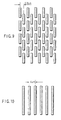
- FIG. 4 schematically shows an alignment mark formed by combination of different patterns on the same photomask.
- FIGS. 5A and 5B collectively show schematically a mark for inspecting the deviation of overlay formed by the combination of different patterns on the same photomask.
- the fourth embodiment covers the case where a first photomask and a second photomask are used in the lithography steps included in the manufacturing process of a semiconductor device, and is featured in that, when the light exposure is performed by using the first or second photomask, a mark for inspecting the deviation of overlay of the photomask and an alignment mark are constructed to include at least a part of the device pattern included in the photomask, and that an alignment mark and a mark for inspecting the deviation of overlay are formed by the combination of different patterns on the same photomask.
- the length in the longitudinal direction is rendered very large compared with the device pattern, even if the pattern size in the width direction corresponds to the device pattern. In such a case, there is a possibility of occurring an inconvenience that is not expected in the device pattern to take place in the process of consecutively executing these marks.
- the alignment mark is divided for use as shown in FIG. 4.
- the mark for inspecting the deviation of overlay is also divided as shown in FIGS. 5A and 5B.
- each of the fine patterns and the thick patterns is divided into a plurality of small patterns.
- an alignment mark consisting of a thick pattern 42 and a fine pattern 43 is formed on the first photomask 41.
- the alignment mark is transferred onto the wafer by using the particular alignment mark formed on the first photomask 41.
- the fine pattern in a position that should originally be transferred is actually deviated in its position so as to actually allow a fine pattern to be transferred in a deviated position.
- the rate of the positional deviation of the fine pattern is larger than that of the thick pattern. Since the thick pattern and the fine pattern differ from each other in the amount of the positional error when transferred onto the wafer, each of the position of the thick pattern and the position of the fine pattern is measured by a signal processing in view of the difference in the generation amount of the positional error noted above.
- the mark for inspecting the deviation of overlay for a large pattern comprises a thick pattern 45 formed of the first photomask and another thick pattern 46 formed of the second photomask.
- the mark for inspecting the deviation of overlay for a small pattern comprises a thick pattern 47 formed of the first photomask and a fine pattern 48 formed of the second photomask.
- the reference patterns 64 and 65 shown in FIGS. 3B and 3C can also be divided for use as in the third embodiment. With the particular construction, it is possible to measure the deviation of alignment for each of the patterns.
- FIGS. 6A to 6E are cross sectional views collectively showing the manufacturing process of a semiconductor device. Described in the following is manufacturing steps of a semiconductor device by employing the alignment method of the present invention.
- a silicon oxide (SiO 2 ) film 73 is formed on a semiconductor substrate 70 such as a silicon semiconductor substrate, followed by forming a photoresist film 74 on the silicon oxide film 73, as shown in FIG. 6A. Further, the photoresist film 74 is selectively exposed to light by using a first photomask 71 described previously in conjunction with the first to fourth embodiments, followed by the developing treatment to form open portions.
- the silicon oxide film 73 is etched with the photoresist 74 used as a mask so as to form contact holes in the silicon oxide film 73, followed by forming a first layer aluminum wiring 75 on the silicon oxide film 73, as shown in FIG. 6B.
- the first layer aluminum wiring 75 is electrically connected to the semiconductor substrate 70 via the contact holes.
- a silicon oxide (SiO 2 ) film 76 is formed in a manner to cover the upper surface of the first layer aluminum wiring 75, followed by planarizing the surface of the silicon oxide film 76 by CMP, as shown in FIG. 6C.
- a photoresist film 77 is formed on the silicon oxide film 76.
- the photoresist film 77 is then selectively exposed to light by using a second photomask 72 of the construction equal to that described previously in conjunction with the first to fourth embodiments so as to form an open portion, as shown in FIG. 6D.
- the silicon oxide film 76 is etched with the photoresist film 77 used as a mask so as to form a contact hole in the silicon oxide film 76.
- a second layer aluminum wiring 78 is formed on the silicon oxide film 76, followed by patterning the second layer aluminum wiring 78.
- the second layer aluminum wiring 78 is electrically connected to the first layer aluminum wiring 75 via the contact hole, as shown in FIG. 6E.
- each of the first and second photomasks is constructed such that each of the alignment mark and the mark for inspecting the deviation of overlay includes a part of the device pattern or an equivalent pattern as in the first embodiment. It follows that the alignment mark and the mark for inspecting the deviation of overlay receive the error caused by the influence given by the aberration of the projection optical system including a projection lens used in performing the pattern transfer in substantially the same degree. As a result, the amount of the positional deviation of the pattern is the same, making it possible to achieve an alignment of a high accuracy, i.e., formation of the device pattern.
- FIG. 7 schematically shows that a large number of chips 11 are formed on the wafer 1 such as a silicon wafer.
- the chips 11 are arranged on the wafer 1 to form a two dimensional array, and dicing lines 12 are formed between the adjacent chips 11.
- the wafer 1 is cut along the dicing lines 12 so as to obtain a plurality of the individual chips 11.
- the alignment mark and the mark for inspecting the deviation of overlay referred to in each of the first to fourth embodiments of the present invention described above are constructed as follows:
- each of the alignment mark and the mark for inspecting the deviation of overlay includes a part of the device pattern or an equivalent pattern, these marks receive an error caused by the influence given by the aberration of the projection optical system used in performing the pattern transfer in substantially the same degree as the device pattern. This implies that the positional deviation amount of these patterns is the same, with the result that it is possible to expect an alignment of a high accuracy. It is also possible to perform the measurement with a high accuracy in measuring the error in the overlay. It should also be noted that, in the case of including a plurality of patterns differing from each other in the size and shape of the device pattern, it is possible to achieve an alignment of a high accuracy even if the positional deviation amount caused by, for example, the aberration of the projection optical system differs depending on the pattern.
Landscapes
- Physics & Mathematics (AREA)
- General Physics & Mathematics (AREA)
- Exposure And Positioning Against Photoresist Photosensitive Materials (AREA)
- Preparing Plates And Mask In Photomechanical Process (AREA)
- Exposure Of Semiconductors, Excluding Electron Or Ion Beam Exposure (AREA)
Abstract
Description
Claims (16)
- An alignment method, characterized by comprising the steps of:forming at least a first device pattern (4) and an alignment mark (25A) on a wafer (1), using a first photomask (21) having the first device pattern and the alignment mark which has a shape equal to or similar to that of said first device pattern; andpositioning a second photomask (22) with respect to a resist film (22A) formed on said wafer (1) according to said alignment mark (25A) formed on said wafer.
- An alignment method according to claim 1, characterized by further comprising the steps of:forming on said wafer a first deviation inspection mark (5A) together with said first device pattern (4) and said alignment mark (25A), using said first photomask (21) having the first deviation inspection mark in addition to the first device pattern and the alignment mark;positioning said second photomask (22) with respect to the alignment mark and the first deviation inspection mark formed on said wafer, said second photomask having a second device pattern and a second deviation inspection mark (43) which has a shape equal to or similar to that of said second device pattern; andforming, at a position on said resist film (22A) corresponding to said first deviation inspection mark, an exposure pattern of said second deviation inspection mark, together with said second device pattern.
- An alignment method according to claim 1, characterized by further comprising the steps of:forming the alignment mark (31) and the first device pattern on the wafer by using the first photomask (21) having the first device pattern including first and second device pattern elements with different sizes and shapes and alignment mark including first and second alignment mark elements (32, 33) with sizes and shapes corresponding to those of the first and second device pattern elements; andpositioning said second photomask (22) with respect to said wafer according to positions of said first and second alignment mark elements of the alignment mark.
- An alignment method according to claim 3, characterized in that said first alignment mark element (32) has a size and a shape to cause an exposure position deviation amount due to an optical system of an exposure apparatus for exposing the resist film being smaller than that caused by said second alignment mark element (33).
- An alignment method according to claim 2, characterized in that said first photomask has first and second deviation inspection reference marks (35, 37) having similar size and shape with each other; andsaid second photomask has a first inspection mark (36) with a size and shape similar to said first deviation inspection reference mark, the first inspection mark being positioned on said wafer in association with said first deviation inspection reference mark, and has a second inspection mark (38) causing an exposure deviation amount due to an optical system of an exposure apparatus used for exposing said resist film larger than that of said first inspection mark, the second inspection mark (38) being positioned on said wafer in association with said second deviation inspection reference mark (37); andthe alignment method further comprising the steps of:
correcting the exposure positions of the first and second photomasks (21, 22) using selectively one of a first arrangement (35, 36) or a second arrangement (37, 38) according to the size and shape of the device pattern formed in said second photomask, the first arrangement being a combination of said first deviation inspection reference mark and said first inspection mark and the second arrangement being a combination of said second deviation inspection reference mark and said second inspection mark. - An alignment method according to claim 2, characterized in that said first photomask (21) has a first deviation inspection mark, a first reference mark (64), and a second deviation inspection mark (65) which has a size and a shape equal to or similar to said first device pattern deviated largely caused by the optical system of an exposure apparatus with respect to the first reference pattern; andsaid second photomask (22) has a second reference mark (65), a third deviation inspection mark (66) which has a size and a shape equal to or similar to said second device pattern deviated largely caused by the optical system of the exposure apparatus with respect to the second reference pattern, and a fourth inspection mark (62) positioned in association with the first deviation inspection mark formed on said wafer; andthe alignment method further comprising the steps of:calculating a sum of a first deviation between said first and fourth deviation inspection marks (64, 63), a second deviation between said first reference pattern and said second deviation inspection mark (65, 66), and a third deviation between said second reference pattern and said third deviation inspection mark (61, 62); andcorrecting an exposure position of another photomask using the calculated sum.
- An overlay inspection method for a photomask, characterized by comprising the steps of:forming on a wafer (1) a first device pattern and an alignment mark, using a first photomask (21) having at least the first device pattern and the alignment mark (41) which has a shape equal to or similar to the first device pattern;exposing a resist film (21A) formed on the wafer (1) to the second photomask (22) according to the alignment mark; anddetermining the positioning accuracy of the second photomask (22) with respect to the wafer (1) using the alignment mark (41).
- An overlay inspection method according to claim 7, characterized by further comprising the steps of:forming on said wafer (1) a first deviation inspection mark together with said first device pattern and said alignment mark, using said first photomask (21) having the first deviation inspection mark in addition to the first device pattern and the alignment mark (41);positioning said second photomask (22) with respect to the alignment mark (41) and the first deviation inspection mark formed on said wafer, said second photomask having a second device pattern and a second deviation inspection mark (42) which has a shape equal to or similar to that of said second device pattern; andforming, at a position on said resist film (22A) corresponding to said first deviation inspection mark, an exposure pattern of said second deviation inspection mark, together with said second device pattern.
- An overlay inspection method according to claim 7, characterized by further comprising the steps of:forming the alignment mark and the first device pattern on the wafer (1) by using the first photomask (21) having the first device pattern including first and second device pattern elements with different sizes and shapes and alignment mark including first and second alignment mark elements (32, 33) with sizes and shapes corresponding to those of the first and second device pattern elements; andpositioning said second photomask (22) with respect to said wafer according to positions of said first and second alignment mark elements (32, 33) of the alignment mark.
- An overlay inspection method according to claim 9, characterized in that said first alignment mark element (32) has a size and a shape to cause an exposure position deviation amount due to an optical system of an exposure apparatus for exposing the resist film being smaller than that caused by said second alignment mark (33).
- An overlay inspection method according to claim 8, characterized in that said first photomask (21) has first and second deviation inspection reference marks (35, 37) having similar size and shape with each other; andsaid second photomask (22) has a first inspection mark (36) with a size and shape similar to said first deviation inspection reference mark, the first inspection mark being positioned on said wafer in association with said first deviation inspection reference mark, and has a second inspection mark (38) causing an exposure deviation amount due to an optical system of an exposure apparatus used for exposing said resist film larger than that of said first inspection mark, the second inspection mark being positioned on said wafer in association with said second deviation inspection reference mark (37); andthe overlay inspection method further comprising the steps of:
correcting the exposure positions of the first and second photomasks (21, 22) using selectively one of a first arrangement or a second arrangement according to the size and shape of the device pattern formed in said second photomask, the first arrangement (35, 36) being a combination of said first deviation inspection reference mark and said first inspection mark and the second arrangement (37, 38) being a combination of said second deviation inspection reference mark and said second inspection mark. - An overlay inspection method according to claim 8, characterized in that said first photomask (21) has a first deviation inspection mark (61), a first reference mark (64), and a second deviation inspection mark (63) which has a size and a shape equal to or similar to said first device pattern deviated largely caused by the optical system of an exposure apparatus with respect to the first reference pattern; andsaid second photomask has a second reference mark (65), a third deviation inspection mark (66) which has a size and a shape equal to or similar to said second device pattern deviated largely caused by the optical system of the exposure apparatus with respect to the second reference pattern, and a fourth inspection mark (62) positioned in association with the first deviation inspection mark formed on said wafer; andthe overlay inspection method further comprising the steps of:calculating a sum of a first deviation between said first and fourth deviation inspection marks (61, 62), a second deviation between said first reference pattern and said second deviation inspection mark (64, 63), and a third deviation between said second reference pattern and said third deviation inspection mark (65, 66); andcorrecting an exposure position of another photomask using the calculated sum.
- A photomask characterized by comprising:a device pattern (4);an alignment mark (25A) having a size and a shape equal to or similar to those of said device pattern; anda deviation inspection mark (5A) having a size and a shape equal to or similar to those of said device pattern.
- A photomask characterized by comprising:a device pattern configuration (4) including at least two device patterns having different sizes and shapes;an alignment mark including at least two alignment mark elements (32, 33) having different sizes and shapes corresponding to those of the device patterns; anda deviation inspection mark (37, 38) having a shape including a part of said device pattern configuration.
- A photomask characterized by comprising:a device pattern configuration (4);an alignment mark including a reference pattern (32) and a part (33) of said device pattern configuration; anda deviation inspection mark having a shape including a part of said device pattern configuration.
- A photomask according to any one of claims 8 to 15, characterized in that said alignment mark (32, 33) and said deviation inspection mark (35-38) respectively have a width and a length corresponding to those of said device pattern configuration.
Applications Claiming Priority (2)
| Application Number | Priority Date | Filing Date | Title |
|---|---|---|---|
| JP2000172077 | 2000-06-08 | ||
| JP2000172077 | 2000-06-08 |
Publications (3)
| Publication Number | Publication Date |
|---|---|
| EP1162507A2 true EP1162507A2 (en) | 2001-12-12 |
| EP1162507A3 EP1162507A3 (en) | 2005-01-05 |
| EP1162507B1 EP1162507B1 (en) | 2007-03-07 |
Family
ID=18674534
Family Applications (1)
| Application Number | Title | Priority Date | Filing Date |
|---|---|---|---|
| EP01112985A Expired - Lifetime EP1162507B1 (en) | 2000-06-08 | 2001-06-08 | Alignment method, overlay deviation inspection method and photomask |
Country Status (6)
| Country | Link |
|---|---|
| US (1) | US6610448B2 (en) |
| EP (1) | EP1162507B1 (en) |
| KR (1) | KR100424228B1 (en) |
| CN (1) | CN100468623C (en) |
| DE (1) | DE60127029T2 (en) |
| TW (1) | TW588414B (en) |
Cited By (10)
| Publication number | Priority date | Publication date | Assignee | Title |
|---|---|---|---|---|
| US6858948B2 (en) | 2001-05-23 | 2005-02-22 | Asml Netherlands B.V. | Substrate provided with an alignment mark in a substantially transmissive process layer, mask for exposing said mark, device manufacturing method, and device manufactured thereby |
| EP1498779A3 (en) * | 2003-07-11 | 2005-03-23 | ASML Netherlands B.V. | Marker structure for alignment or overlay |
| DE10345466A1 (en) * | 2003-09-30 | 2005-04-28 | Infineon Technologies Ag | A method of detecting placement errors of circuit patterns when transferred by a mask to layers of a substrate of a semiconductor wafer |
| WO2005041291A3 (en) * | 2003-10-15 | 2005-12-29 | Infineon Technologies Ag | Mask and method for using the mask in lithographic processing |
| WO2005064408A3 (en) * | 2003-12-23 | 2006-03-02 | Koninkl Philips Electronics Nv | Wafer with optical control modules in exposure fields |
| US7466413B2 (en) | 2003-07-11 | 2008-12-16 | Asml Netherlands B.V. | Marker structure, mask pattern, alignment method and lithographic method and apparatus |
| CN102053479B (en) * | 2009-10-28 | 2012-11-21 | 中芯国际集成电路制造(上海)有限公司 | Positioning device and positioning method for optical mask defects |
| CN111900116A (en) * | 2020-06-22 | 2020-11-06 | 中国科学院微电子研究所 | Wafer alignment method and system |
| CN112652566A (en) * | 2020-12-30 | 2021-04-13 | 合肥晶合集成电路股份有限公司 | Method for preparing integrated circuit |
| CN114326332A (en) * | 2022-01-28 | 2022-04-12 | 魅杰光电科技(上海)有限公司 | Alignment mark for exposure device and alignment method thereof |
Families Citing this family (66)
| Publication number | Priority date | Publication date | Assignee | Title |
|---|---|---|---|---|
| JP3348783B2 (en) * | 1999-07-28 | 2002-11-20 | 日本電気株式会社 | Mark for overlay and semiconductor device |
| US7804994B2 (en) * | 2002-02-15 | 2010-09-28 | Kla-Tencor Technologies Corporation | Overlay metrology and control method |
| DE10230532B4 (en) * | 2002-07-05 | 2007-03-08 | Infineon Technologies Ag | Method for determining the structure of a mask for microstructuring semiconductor substrates by means of photolithography |
| DE10248224B4 (en) * | 2002-10-16 | 2005-08-04 | Infineon Technologies Ag | Method for adjusting and exposing a semiconductor wafer |
| US7075639B2 (en) * | 2003-04-25 | 2006-07-11 | Kla-Tencor Technologies Corporation | Method and mark for metrology of phase errors on phase shift masks |
| JP2004342833A (en) * | 2003-05-15 | 2004-12-02 | Seiko Epson Corp | Semiconductor device manufacturing method, electro-optical device, integrated circuit, and electronic equipment. |
| US7346878B1 (en) | 2003-07-02 | 2008-03-18 | Kla-Tencor Technologies Corporation | Apparatus and methods for providing in-chip microtargets for metrology or inspection |
| US7608468B1 (en) * | 2003-07-02 | 2009-10-27 | Kla-Tencor Technologies, Corp. | Apparatus and methods for determining overlay and uses of same |
| CN100510967C (en) * | 2003-08-04 | 2009-07-08 | 麦克罗尼克激光系统公司 | Phase shift mask alignment method and device |
| DE10345524B4 (en) * | 2003-09-30 | 2005-10-13 | Infineon Technologies Ag | Method for determining a relative offset of two structured circuit patterns on a semiconductor wafer by means of a scanning electron microscope |
| US7425396B2 (en) * | 2003-09-30 | 2008-09-16 | Infineon Technologies Ag | Method for reducing an overlay error and measurement mark for carrying out the same |
| DE10359200B4 (en) * | 2003-09-30 | 2012-10-31 | Qimonda Ag | Method for reducing a coverage error |
| CN100382229C (en) * | 2003-10-08 | 2008-04-16 | 茂德科技股份有限公司 | Alignment mark capable of correcting manufacturing process deviation and alignment method thereof |
| US7241538B2 (en) * | 2003-11-05 | 2007-07-10 | Promos Technologies | Method for providing representative features for use in inspection of photolithography mask and for use in inspection photo-lithographically developed and/or patterned wafer layers, and products of same |
| WO2005076077A2 (en) * | 2004-02-05 | 2005-08-18 | Koninklijke Philips Electronics N. V. | Mask inspection apparatus and method |
| EP1569276A1 (en) * | 2004-02-27 | 2005-08-31 | Heptagon OY | Micro-optics on optoelectronics |
| US7557921B1 (en) | 2005-01-14 | 2009-07-07 | Kla-Tencor Technologies Corporation | Apparatus and methods for optically monitoring the fidelity of patterns produced by photolitographic tools |
| JP4290177B2 (en) * | 2005-06-08 | 2009-07-01 | キヤノン株式会社 | Mold, alignment method, pattern forming apparatus, pattern transfer apparatus, and chip manufacturing method |
| JP2007035768A (en) * | 2005-07-25 | 2007-02-08 | Toshiba Corp | Method for forming misalignment inspection mark and method for manufacturing semiconductor device |
| TWI302341B (en) * | 2006-08-04 | 2008-10-21 | Nanya Technology Corp | Improved overlay mark |
| CN101174092B (en) * | 2006-10-30 | 2010-10-06 | 上海华虹Nec电子有限公司 | Method for monitoring imaging distortion caused by lens coma aberration and lens imaging system thereof |
| CN100456141C (en) * | 2007-01-23 | 2009-01-28 | 上海微电子装备有限公司 | Batch Wafer Exposure Method |
| CN101398630B (en) * | 2007-09-25 | 2010-10-13 | 南亚科技股份有限公司 | Alignment and overlay mark, mask structure and using method thereof |
| JP2009238777A (en) * | 2008-03-25 | 2009-10-15 | Toshiba Corp | Manufacturing method of semiconductor device |
| KR100984271B1 (en) * | 2008-12-24 | 2010-10-04 | 김주환 | Calibration method of mask inspection device |
| CN101789386B (en) * | 2009-01-24 | 2011-09-21 | 南亚科技股份有限公司 | Wafer Alignment Method |
| CN101924013B (en) * | 2009-06-17 | 2012-10-03 | 上海华虹Nec电子有限公司 | Method for increasing photo-etching alignment precision after extension |
| CN102005361B (en) * | 2009-09-03 | 2012-07-11 | 上海华虹Nec电子有限公司 | Forming method of aligned layer graphs on silicon wafer |
| US8039356B2 (en) * | 2010-01-20 | 2011-10-18 | International Business Machines Corporation | Through silicon via lithographic alignment and registration |
| US9927718B2 (en) | 2010-08-03 | 2018-03-27 | Kla-Tencor Corporation | Multi-layer overlay metrology target and complimentary overlay metrology measurement systems |
| CN102386322B (en) * | 2010-08-25 | 2013-07-24 | 中芯国际集成电路制造(上海)有限公司 | Method for improving aligning accuracy |
| CN101982880A (en) * | 2010-09-10 | 2011-03-02 | 上海集成电路研发中心有限公司 | Registration measurement pattern |
| CN102456540B (en) * | 2010-10-19 | 2014-05-21 | 上海华虹宏力半导体制造有限公司 | Method for preparing photoetching alignment mark applied to epitaxial process |
| CN102540732A (en) * | 2010-12-08 | 2012-07-04 | 无锡华润上华科技有限公司 | Method for judging one-time photoetching result during semiconductor production |
| CN102540735A (en) * | 2010-12-08 | 2012-07-04 | 无锡华润上华科技有限公司 | Check method of photomask diagram position deviation |
| CN102543667B (en) * | 2010-12-08 | 2014-02-26 | 上海华虹宏力半导体制造有限公司 | Forming method of graph of aligned layer on silicon chip |
| JP5533769B2 (en) * | 2011-04-14 | 2014-06-25 | ウシオ電機株式会社 | Mask and workpiece alignment method |
| CN102364301A (en) * | 2011-06-30 | 2012-02-29 | 常州天合光能有限公司 | Method for Measuring Stencil Overlay Accuracy |
| US10890436B2 (en) | 2011-07-19 | 2021-01-12 | Kla Corporation | Overlay targets with orthogonal underlayer dummyfill |
| US9097978B2 (en) * | 2012-02-03 | 2015-08-04 | Taiwan Semiconductor Manufacturing Company, Ltd. | Method and apparatus to characterize photolithography lens quality |
| JP5696079B2 (en) | 2012-03-22 | 2015-04-08 | 株式会社東芝 | Mask and semiconductor device manufacturing method |
| JP5832345B2 (en) * | 2012-03-22 | 2015-12-16 | 株式会社ニューフレアテクノロジー | Inspection apparatus and inspection method |
| US20140240705A1 (en) * | 2013-02-27 | 2014-08-28 | Kabushiki Kaisha Toshiba | Semiconductor device, reticle method for checking position misalignment and method for manufacturing position misalignment checking mark |
| CN103247550B (en) * | 2013-05-07 | 2016-04-13 | 上海华力微电子有限公司 | The test module of monitoring program stability and method |
| CN104347443B (en) * | 2013-08-07 | 2017-02-08 | 无锡华润上华科技有限公司 | Testing method for sudden change in horizontal direction of wafer alignment |
| JP6271922B2 (en) * | 2013-09-10 | 2018-01-31 | キヤノン株式会社 | Method for determining position, exposure method, exposure apparatus, and article manufacturing method |
| WO2016060545A1 (en) * | 2014-10-14 | 2016-04-21 | Mimos Berhad | Overlay feature design and method for application in wafer fabrication |
| CN105824198B (en) * | 2015-01-04 | 2019-01-18 | 上海微电子装备(集团)股份有限公司 | A kind of multiple exposing method |
| CN106324979B (en) * | 2015-07-02 | 2020-03-27 | 无锡华润华晶微电子有限公司 | Mask plate, wafer positioning plate, manufacturing method and wafer manufacturing method |
| US9470987B1 (en) * | 2015-10-22 | 2016-10-18 | United Microelectronics Corp. | Overlay mask |
| KR101665569B1 (en) * | 2016-05-19 | 2016-10-12 | (주)오로스 테크놀로지 | Overlay mark, overlay measurement method and semiconductor device manufacturing method using the overlay mark |
| US9786569B1 (en) | 2016-10-26 | 2017-10-10 | Taiwan Semiconductor Manufacturing Co., Ltd. | Overlay measurement and compensation in semiconductor fabrication |
| US10871708B2 (en) | 2017-01-24 | 2020-12-22 | Nikon Corporation | Spatial-frequency matched wafer alignment marks, wafer alignment and overlay measurement and processing using multiple different mark designs on a single layer |
| JP2018185452A (en) * | 2017-04-27 | 2018-11-22 | ルネサスエレクトロニクス株式会社 | Semiconductor device and manufacturing method thereof |
| CN107367249B (en) * | 2017-07-27 | 2019-11-26 | 四川省建筑科学研究院有限公司 | Prefabricated components assembling capacity detection method, method of adjustment and joining method |
| US10474040B2 (en) * | 2017-12-07 | 2019-11-12 | Kla-Tencor Corporation | Systems and methods for device-correlated overlay metrology |
| US10533848B2 (en) * | 2018-03-05 | 2020-01-14 | Kla-Tencor Corporation | Metrology and control of overlay and edge placement errors |
| CN108766901B (en) * | 2018-06-26 | 2020-07-31 | 上海华力微电子有限公司 | Method for detecting flatness of wafer worktable |
| JP2020041859A (en) | 2018-09-07 | 2020-03-19 | キオクシア株式会社 | Position measuring method, position measuring device, and semiconductor device manufacturing method |
| EP3931865A4 (en) * | 2019-02-14 | 2023-02-15 | KLA Corporation | SYSTEM AND METHOD FOR MEASURING MISALIGNMENT OF SEMICONDUCTOR DEVICE WAFER USING INDUCED TOPOGRAPHY |
| CN112034677B (en) * | 2020-09-17 | 2024-02-06 | 合肥晶合集成电路股份有限公司 | Overlay mark, overlay mark method and overlay measurement method |
| CN112394611B (en) * | 2020-11-16 | 2024-02-23 | 长江存储科技有限责任公司 | Mask plate and method of making three-dimensional memory |
| CN112130414B (en) * | 2020-11-26 | 2021-04-06 | 中芯集成电路制造(绍兴)有限公司 | Calibration method for feeding position of photolithography mask and exposure machine |
| CN112612185B (en) * | 2020-12-15 | 2022-11-22 | 长江存储科技有限责任公司 | Pattern structure and method for overlay error detection |
| CN114428445A (en) * | 2022-01-27 | 2022-05-03 | 华虹半导体(无锡)有限公司 | Overlay error measurement method and device |
| CN114995077B (en) * | 2022-06-21 | 2025-05-27 | 广州新锐光掩模科技有限公司 | A method for aligning pattern positions between EUV lithography machine and DUV lithography machine |
Family Cites Families (15)
| Publication number | Priority date | Publication date | Assignee | Title |
|---|---|---|---|---|
| US4475811A (en) | 1983-04-28 | 1984-10-09 | The Perkin-Elmer Corporation | Overlay test measurement systems |
| JP2836391B2 (en) * | 1992-07-30 | 1998-12-14 | 日本電気株式会社 | Mask for fabricating semiconductor integrated circuit and inspection method thereof |
| JP2829211B2 (en) * | 1993-01-07 | 1998-11-25 | 株式会社東芝 | Misalignment measurement method |
| US5702567A (en) | 1995-06-01 | 1997-12-30 | Kabushiki Kaisha Toshiba | Plurality of photolithographic alignment marks with shape, size and spacing based on circuit pattern features |
| US5757507A (en) * | 1995-11-20 | 1998-05-26 | International Business Machines Corporation | Method of measuring bias and edge overlay error for sub-0.5 micron ground rules |
| JPH09244222A (en) * | 1996-03-08 | 1997-09-19 | Mitsubishi Electric Corp | Reticle for overlay error measurement, overlay error measurement method and overlay error measurement mark using the reticle |
| TW361055B (en) | 1996-05-09 | 1999-06-11 | Mitsubishi Electric Corp | Mark for measurement of accuracy in superposition, method for correcting detect of the mark, photomask having the mark, and manufacture and exposure device for the photomask |
| KR200148125Y1 (en) * | 1996-08-30 | 1999-06-15 | 구본준 | Photomask |
| JP3684707B2 (en) * | 1996-09-30 | 2005-08-17 | 富士通株式会社 | Reticle pattern inspection method |
| KR19980031846A (en) * | 1996-10-31 | 1998-07-25 | 김영환 | Manufacturing Method of Semiconductor Device |
| JP3892565B2 (en) * | 1997-02-28 | 2007-03-14 | 株式会社東芝 | Pattern formation method |
| US5902703A (en) * | 1997-03-27 | 1999-05-11 | Vlsi Technology, Inc. | Method for measuring dimensional anomalies in photolithographed integrated circuits using overlay metrology, and masks therefor |
| JP3757551B2 (en) * | 1997-06-25 | 2006-03-22 | ソニー株式会社 | Mask pattern forming method and mask formed by this method |
| JP3580992B2 (en) * | 1997-09-18 | 2004-10-27 | 旭化成マイクロシステム株式会社 | Photo mask |
| JP2000133576A (en) * | 1998-10-28 | 2000-05-12 | Nec Corp | Misalignment measurement mark and misalignment measurement method |
-
2001
- 2001-06-05 TW TW090113628A patent/TW588414B/en not_active IP Right Cessation
- 2001-06-07 US US09/874,958 patent/US6610448B2/en not_active Expired - Lifetime
- 2001-06-08 DE DE60127029T patent/DE60127029T2/en not_active Expired - Lifetime
- 2001-06-08 EP EP01112985A patent/EP1162507B1/en not_active Expired - Lifetime
- 2001-06-08 KR KR10-2001-0032023A patent/KR100424228B1/en not_active Expired - Fee Related
- 2001-06-08 CN CNB011208767A patent/CN100468623C/en not_active Expired - Fee Related
Cited By (18)
| Publication number | Priority date | Publication date | Assignee | Title |
|---|---|---|---|---|
| US6876092B2 (en) | 2001-05-23 | 2005-04-05 | Asml Netherlands B.V. | Substrate provided with an alignment mark, method of designing a mask, computer program, mask for exposing said mark, device manufacturing method, and device manufactured thereby |
| US6858948B2 (en) | 2001-05-23 | 2005-02-22 | Asml Netherlands B.V. | Substrate provided with an alignment mark in a substantially transmissive process layer, mask for exposing said mark, device manufacturing method, and device manufactured thereby |
| US7759029B2 (en) | 2001-05-23 | 2010-07-20 | Asml Netherlands B.V. | Substrate provided with an alignment mark in a substantially transmissive process layer, mask for exposing said mark, device manufacturing method, and device manufactured thereby |
| US7560196B2 (en) | 2001-05-23 | 2009-07-14 | Asml Netherlands B.V. | Mask for exposing an alignment mark, and method and computer program for designing the mask |
| US7056805B2 (en) | 2001-05-23 | 2006-06-06 | Asml Netherlands B.V. | Substrate provided with an alignment mark in a substantially transmissive process layer, mask for exposing said mark, device manufacturing method, and device manufactured thereby |
| US7462548B2 (en) | 2001-05-23 | 2008-12-09 | Asml Netherlands B.V. | Substrate provided with an alignment mark in a substantially transmissive process layer, mask for exposing said mark, device manufacturing method, and device manufactured thereby |
| US7466413B2 (en) | 2003-07-11 | 2008-12-16 | Asml Netherlands B.V. | Marker structure, mask pattern, alignment method and lithographic method and apparatus |
| EP1498779A3 (en) * | 2003-07-11 | 2005-03-23 | ASML Netherlands B.V. | Marker structure for alignment or overlay |
| DE10345466A1 (en) * | 2003-09-30 | 2005-04-28 | Infineon Technologies Ag | A method of detecting placement errors of circuit patterns when transferred by a mask to layers of a substrate of a semiconductor wafer |
| WO2005041291A3 (en) * | 2003-10-15 | 2005-12-29 | Infineon Technologies Ag | Mask and method for using the mask in lithographic processing |
| US7030506B2 (en) | 2003-10-15 | 2006-04-18 | Infineon Technologies, Ag | Mask and method for using the mask in lithographic processing |
| WO2005064408A3 (en) * | 2003-12-23 | 2006-03-02 | Koninkl Philips Electronics Nv | Wafer with optical control modules in exposure fields |
| CN102053479B (en) * | 2009-10-28 | 2012-11-21 | 中芯国际集成电路制造(上海)有限公司 | Positioning device and positioning method for optical mask defects |
| CN111900116A (en) * | 2020-06-22 | 2020-11-06 | 中国科学院微电子研究所 | Wafer alignment method and system |
| CN112652566A (en) * | 2020-12-30 | 2021-04-13 | 合肥晶合集成电路股份有限公司 | Method for preparing integrated circuit |
| CN112652566B (en) * | 2020-12-30 | 2023-03-07 | 合肥晶合集成电路股份有限公司 | Method for preparing integrated circuit |
| CN114326332A (en) * | 2022-01-28 | 2022-04-12 | 魅杰光电科技(上海)有限公司 | Alignment mark for exposure device and alignment method thereof |
| CN114326332B (en) * | 2022-01-28 | 2024-03-26 | 魅杰光电科技(上海)有限公司 | Alignment mark for exposure device and alignment method thereof |
Also Published As
| Publication number | Publication date |
|---|---|
| KR100424228B1 (en) | 2004-03-24 |
| EP1162507A3 (en) | 2005-01-05 |
| US6610448B2 (en) | 2003-08-26 |
| TW588414B (en) | 2004-05-21 |
| US20010055720A1 (en) | 2001-12-27 |
| DE60127029D1 (en) | 2007-04-19 |
| CN100468623C (en) | 2009-03-11 |
| KR20010111048A (en) | 2001-12-15 |
| CN1329357A (en) | 2002-01-02 |
| EP1162507B1 (en) | 2007-03-07 |
| DE60127029T2 (en) | 2007-11-15 |
Similar Documents
| Publication | Publication Date | Title |
|---|---|---|
| EP1162507B1 (en) | Alignment method, overlay deviation inspection method and photomask | |
| JP4528464B2 (en) | Alignment method, overlay inspection method, and photomask | |
| US6670632B1 (en) | Reticle and method of fabricating semiconductor device | |
| JP4864776B2 (en) | Photo mask | |
| US6498640B1 (en) | Method to measure alignment using latent image grating structures | |
| US7160654B2 (en) | Method of the adjustable matching map system in lithography | |
| US7972932B2 (en) | Mark forming method and method for manufacturing semiconductor device | |
| US8497997B2 (en) | Semiconductor device and method of manufacturing the same | |
| US5783341A (en) | Alignment for layer formation through determination of target values for translation, rotation and magnification | |
| JPH1069066A (en) | Mask and its inspection method and exposure method | |
| KR100519252B1 (en) | Overlay mark, method for forming overlay mark and mearsurement method for overlay | |
| KR100257167B1 (en) | Method of manufacturing semiconductor device | |
| US20040241558A1 (en) | Focus detection structure | |
| US7483156B2 (en) | Method for measuring overlay and overlay mark used therefor | |
| US6841307B2 (en) | Photomask making method and alignment method | |
| JPH11132716A (en) | Overlapping accuracy measuring method in photolithography process and overlapping accuracy measuring mark in photolithography process | |
| JP2970473B2 (en) | Alignment method and alignment error inspection method | |
| JP2000306822A (en) | Method for manufacturing semiconductor device | |
| JP2004273612A (en) | Semiconductor device, manufacturing method thereof, and photomask | |
| KR20010028305A (en) | Method for revising registration | |
| KR960002287B1 (en) | Stepping pitch measuring method of alignment/exposure apparatus | |
| KR100283483B1 (en) | Method for manufacturing target for measuring overlapping | |
| JPH09304916A (en) | Method for forming alignment mark and / or misalignment measurement mark | |
| JP2002025899A (en) | Alignment mark and alignment method | |
| GB2367146A (en) | Method of fabricating a semiconductor device. |
Legal Events
| Date | Code | Title | Description |
|---|---|---|---|
| PUAI | Public reference made under article 153(3) epc to a published international application that has entered the european phase |
Free format text: ORIGINAL CODE: 0009012 |
|
| 17P | Request for examination filed |
Effective date: 20010608 |
|
| AK | Designated contracting states |
Kind code of ref document: A2 Designated state(s): AT BE CH CY DE DK ES FI FR GB GR IE IT LI LU MC NL PT SE TR |
|
| AX | Request for extension of the european patent |
Free format text: AL;LT;LV;MK;RO;SI |
|
| PUAL | Search report despatched |
Free format text: ORIGINAL CODE: 0009013 |
|
| AK | Designated contracting states |
Kind code of ref document: A3 Designated state(s): AT BE CH CY DE DK ES FI FR GB GR IE IT LI LU MC NL PT SE TR |
|
| AX | Request for extension of the european patent |
Extension state: AL LT LV MK RO SI |
|
| 17Q | First examination report despatched |
Effective date: 20050513 |
|
| AKX | Designation fees paid |
Designated state(s): DE FR GB |
|
| GRAP | Despatch of communication of intention to grant a patent |
Free format text: ORIGINAL CODE: EPIDOSNIGR1 |
|
| RIC1 | Information provided on ipc code assigned before grant |
Ipc: G03F 7/20 20060101AFI20060818BHEP Ipc: G03F 9/00 20060101ALI20060818BHEP |
|
| GRAS | Grant fee paid |
Free format text: ORIGINAL CODE: EPIDOSNIGR3 |
|
| GRAA | (expected) grant |
Free format text: ORIGINAL CODE: 0009210 |
|
| AK | Designated contracting states |
Kind code of ref document: B1 Designated state(s): DE FR GB |
|
| REG | Reference to a national code |
Ref country code: GB Ref legal event code: FG4D |
|
| REF | Corresponds to: |
Ref document number: 60127029 Country of ref document: DE Date of ref document: 20070419 Kind code of ref document: P |
|
| ET | Fr: translation filed | ||
| PLBE | No opposition filed within time limit |
Free format text: ORIGINAL CODE: 0009261 |
|
| STAA | Information on the status of an ep patent application or granted ep patent |
Free format text: STATUS: NO OPPOSITION FILED WITHIN TIME LIMIT |
|
| 26N | No opposition filed |
Effective date: 20071210 |
|
| PGFP | Annual fee paid to national office [announced via postgrant information from national office to epo] |
Ref country code: FR Payment date: 20110621 Year of fee payment: 11 |
|
| PGFP | Annual fee paid to national office [announced via postgrant information from national office to epo] |
Ref country code: GB Payment date: 20110608 Year of fee payment: 11 |
|
| PGFP | Annual fee paid to national office [announced via postgrant information from national office to epo] |
Ref country code: DE Payment date: 20110601 Year of fee payment: 11 |
|
| GBPC | Gb: european patent ceased through non-payment of renewal fee |
Effective date: 20120608 |
|
| REG | Reference to a national code |
Ref country code: FR Ref legal event code: ST Effective date: 20130228 |
|
| REG | Reference to a national code |
Ref country code: DE Ref legal event code: R119 Ref document number: 60127029 Country of ref document: DE Effective date: 20130101 |
|
| PG25 | Lapsed in a contracting state [announced via postgrant information from national office to epo] |
Ref country code: DE Free format text: LAPSE BECAUSE OF NON-PAYMENT OF DUE FEES Effective date: 20130101 Ref country code: GB Free format text: LAPSE BECAUSE OF NON-PAYMENT OF DUE FEES Effective date: 20120608 Ref country code: FR Free format text: LAPSE BECAUSE OF NON-PAYMENT OF DUE FEES Effective date: 20120702 |