EP1160880B1 - Process for the mass production of photovoltaic modules - Google Patents
Process for the mass production of photovoltaic modules Download PDFInfo
- Publication number
- EP1160880B1 EP1160880B1 EP01304749A EP01304749A EP1160880B1 EP 1160880 B1 EP1160880 B1 EP 1160880B1 EP 01304749 A EP01304749 A EP 01304749A EP 01304749 A EP01304749 A EP 01304749A EP 1160880 B1 EP1160880 B1 EP 1160880B1
- Authority
- EP
- European Patent Office
- Prior art keywords
- substrate
- layers
- semiconductor material
- type iib
- vib
- Prior art date
- Legal status (The legal status is an assumption and is not a legal conclusion. Google has not performed a legal analysis and makes no representation as to the accuracy of the status listed.)
- Expired - Lifetime
Links
Images


Classifications
-
- H—ELECTRICITY
- H10—SEMICONDUCTOR DEVICES; ELECTRIC SOLID-STATE DEVICES NOT OTHERWISE PROVIDED FOR
- H10F—INORGANIC SEMICONDUCTOR DEVICES SENSITIVE TO INFRARED RADIATION, LIGHT, ELECTROMAGNETIC RADIATION OF SHORTER WAVELENGTH OR CORPUSCULAR RADIATION
- H10F71/00—Manufacture or treatment of devices covered by this subclass
- H10F71/125—The active layers comprising only Group II-VI materials, e.g. CdS, ZnS or CdTe
-
- Y—GENERAL TAGGING OF NEW TECHNOLOGICAL DEVELOPMENTS; GENERAL TAGGING OF CROSS-SECTIONAL TECHNOLOGIES SPANNING OVER SEVERAL SECTIONS OF THE IPC; TECHNICAL SUBJECTS COVERED BY FORMER USPC CROSS-REFERENCE ART COLLECTIONS [XRACs] AND DIGESTS
- Y02—TECHNOLOGIES OR APPLICATIONS FOR MITIGATION OR ADAPTATION AGAINST CLIMATE CHANGE
- Y02E—REDUCTION OF GREENHOUSE GAS [GHG] EMISSIONS, RELATED TO ENERGY GENERATION, TRANSMISSION OR DISTRIBUTION
- Y02E10/00—Energy generation through renewable energy sources
- Y02E10/50—Photovoltaic [PV] energy
- Y02E10/543—Solar cells from Group II-VI materials
Definitions
- the present invention relates to processes for the mass production of low cost photovoltaic modules and, more specifically to a process for fabricating the critical semiconductor layers, which together with attendant non-vacuum processes, are all accomplished at high throughput.
- PV modules are used to generate electricity from sunlight by the photovoltaic effect. It has been recognized for decades that if these modules could be mass produced at low cost, they could be used to meet a considerable portion of the world's energy needs.
- PV modules must be produced at many times the current volume and at costs below $100/m 2 , as discussed by Bonnet et. al. in "Cadmium-telluride material for thin film solar cells", J. Mater. Res., Vol. 13, No. 10 (1998 ).
- PV modules are manufactured in small quantities at costs of about $500/m 2 . About one hundred times the current yearly production is required to sustain a PV module manufacturing capacity that can contribute just 5% of the current electricity generated. Consequently, the manufacturing volume of PV modules needs to be greatly increased and costs significantly reduced.
- PV modules must be produced as a commodity.
- Commodity level manufacturing requires innovation to develop highly automated production processes and equipment, which are designed to specifically fabricate the commodity product.
- Commodity manufacturing necessitates high production speeds (high throughput), minimal labor costs, and a continuous process flow.
- Low capital costs and ease of expanding production capacity also facilitate commodity manufacturing.
- cadmium telluride (CdTe) thin film PV device has the potential to satisfy the requirements for commodity manufacturing.
- CdTe PV cells are thin film polycrystalline devices, in which the CdTe layer is paired with a cadmium sulfide (CdS) layer to form a heterojunction.
- CdS/CdTe PV device can be produced through a variety of vacuum and non-vacuum processes.
- sublimation in vacuum is most amenable to commodity manufacturing. This is because vacuum sublimation of CdS/CdTe PV modules exhibits deposition rates 10 to 100 times higher than any other PV module deposition method.
- Vacuum sublimation of the semiconductor layers for CdS/CdTe PV modules can also be performed in modest vacuum levels and does not require costly high vacuum equipment. Vacuum deposition methods for other thin film PV devices require costly, complex high vacuum equipment and results in low throughput.
- CdS/CdTe thin film cell fabricated by vacuum sublimation is the most suitable for commodity level manufacturing of PV modules.
- cadmium is a Group B carcinogen. According to U.S. government regulations, the quantity of this material which can be lawfully released into the environment or into an occupational setting is extremely small.
- the known prior art in CdS/CdTe vacuum sublimation requires process and hardware innovations to achieve occupational and environmental safety as required by federal regulations, as well as commodity scale manufacturing.
- a CdTe device is the back wall configuration, in which the thin films are deposited onto a glass superstrate, hereinafter referred to as a substrate.
- the CdTe device is most often fabricated on a glass substrate coated with a transparent conductive oxide (TCO) film onto which other film layers are deposited in the following order: a) a CdS film, b) a CdTe film, c) an ohmic contact layer, and d) a metal film.
- TCO transparent conductive oxide
- the TCO and the metal films form the front and back electrodes, respectively.
- the CdS layer (n-type) and the CdTe layer (p-type) form the p/n junction of the device.
- the cells are deployed with the substrate facing the sun. Photons travel through the glass and TCO film before reaching the p/n junction of the device.
- a module is formed by interconnecting individual cells in series to produce a useful voltage.
- a process for manufacturing CdS/CdTe modules includes the following steps: 1) cleaning the TCO coated glass substrates, 2) heating the substrates, 3) depositing an n-type CdS layer, 4) depositing a p-type CdTe layer, 5) performing a CdCl 2 treatment to improve CdTe grain structure and electrical properties, 6) forming a p+ ohmic low resistance contact layer to improve current collection from the CdTe, 7) depositing a metal layer (metallization) to form the back electrode, 8) scribing the film layers into individual cells, 9) interconnecting the cells in series and providing a means of electrical connection to the module, and 10) encapsulating the finished module.
- Prior art methods for scribing the layers to form a module include laser scribing, mechanical scribing, and abrasive blasting.
- Known laser scribing methods used in the PV industry are associated with low production speed and high capital cost. Laser scribing was abandoned recently in one industrial setting due to laser equipment failure as discussed by Borg in, "Commercial Production of Thin-Film CdTe Photovoltaic Modules", NREL/SR-520-23733, Oct. 1997.
- Known mechanical and abrasive blast scribing methods have only been shown on a small scale as typified by U.S. Patent No. 5,501,744 to Albright and require innovation and improvement to be suitable for commodity level manufacturing.
- VTD vapor transport deposition
- the substrate is held horizontally in a heated environment and supported from beneath by ceramic rollers in the heated environment.
- the deposition of the semiconductor is made onto the top surface of the substrate.
- the ceramic rollers prevent the glass substrate from sagging under its own weight due to the elevated temperatures involved.
- the entire VTD method is very complex and costly. It is possible to deposit a complete CdTe solar cell in a very short time and at sufficiently low substrate temperatures to eliminate glass sagging completely or reduce it to a very small acceptable value. Thus, the expensive ceramic rollers of the VTD method are not needed. Reloading starting material may also be performed in a much simple manner than as shown in this prior art. Since the films are thin, only small amounts of material are required to form them. Consequently, only very small volumes of starting material are needed for many days of operation, thus eliminating the need for this complex reloading arrangement. The heated vessels of this method contain toxic vapors, which pose significant occupational safety problems when they are opened for reloading during processing.
- VTD method vapors are transported through long distances in a carrier gas, an arrangement which will likely lead to the formation of very small nano-particles through condensation of the vapors. These nano-particles degrade the film qualities and lead to occupational hazards when the system is serviced. Furthermore, in the VTD method, the continuous flow of carrier gas has to be maintained along the substrate. Any CdS or CdTe vapors that are carried past the substrate will be wasted. Any deposits of waste material on the inner surface of the vacuum chamber, pumps, exhaust, etc. must be cleaned, thereby exposing maintenance workers to toxic materials and raising occupational safety issues.
- the VTD method In order to prevent unwanted condensation of CdS and CdTe vapors, the VTD method also requires continued heating of large portions of the equipment, including the vaporization vessel itself, the conduits, the deposition chamber, etc. This wastes energy and increases the capital costs.
- the VTD method is only used for depositing the p/n junction layers.
- Other processing steps, such as the CdCl 2 treatment, ohmic contact formation, and metallization are inherently low throughput batch processes. Scribing is taught to be either laser scribing or photolithography, both of which are slow and costly processes.
- An operating pressure of 750 millitorr is specified. At these pressures, nano-particles will be formed, since the vapor will homogeneously condense in the ambient gas near the edge of the deposition space. These very small particles degrade film quality and pose a health hazard to workers during routine maintenance inside the vacuum chamber.
- US4798660 discloses a method for fabricating a copper indium diselenide semiconductor film comprising use of DC magnetron sputtering apparatus to sequentially deposit a first film of copper on a substrate and a second film of indium on the copper film.
- PATENT ABSTRACTS OF JAPAN vol. 010, no. 209 (E-421), 22 July 1986 & JP61049483A disclose a method of manufacturing a photoconductive thin film in which a thin film made of CdS, CdSe or a mixture thereof is deposited on a substrate. This thin film is heat-treated while allowing a powder composed of CdS, CdSe and a small amount of a Cu compound to contact the thin film. Further the film is heat-treated in a mixed vapor of CdS, CdSe and a Cd chloride.
- GB2084197 discloses a method and apparatus for depositing material (e.g. CdS) on a continuously moving substrate by vacuum evaporation, particularly in the manufacture of photovoltaic cells.
- material e.g. CdS
- Any vacuum process for manufacturing CdTe PV modules would also require an apparatus to transport substrates through the process steps within vacuum and to transport the substrates into and out of vacuum rapidly.
- This apparatus should be robust, simple, and low cost. The apparatuses described in the prior art simply do not meet these requirements.
- the present invention is directed to commodity scale manufacturing of CdTe PV modules and involves innovations in manufacturing processes.
- a method for fabricating semiconductor layers of a photovoltaic cell comprising the steps of: providing, in a vacuum chamber, a substrate upon which the photovoltaic cell is to be fabricated; heating the substrate to a desired temperature in the vacuum chamber; depositing one or more layers of n-type IIB/VIB semiconductor material onto a surface of the substrate in the vacuum chamber; depositing one or more layers of p-type IIB/VIB semiconductor material onto the one or more layers of n-type IIB/VIB semiconductor material in the vacuum chamber; the method being characterized in that all steps thereof are carried out in a single vacuum chamber, said vacuum chamber being at a constant vacuum level and in that the method comprises the additional steps of: treating the one or more layers of n-type IIB/VIB and p-type IIB/VIB semiconductor material with the vapor of a halogen containing substance in the vacuum chamber, wherein treating the one or more layers of n-type IIB/VIB and p-type II
- One aspect of the present invention involves providing all of the processing steps for the critical semiconductor layers of a CdTe PV device inline, with all of those steps being completely performed within one vacuum boundary, at high throughput. They include rapid substrate heating, deposition of CdS, deposition of CdTe, CdCl 2 treatment, and ohmic contact formation. These steps are performed at modest vacuum pressures without requiring costly high vacuum equipment.
- inline vacuum processing By utilizing inline vacuum processing to form all of the critical layers without breaking vacuum, an improvement in process throughput, film quality, device efficiency, and device stability is realized, while at the same time avoiding pinhole formation. All inline vacuum processing is also advantageous in that it limits the production of toxic waste and environmental and occupational exposure to toxic compounds.
- a preferred aspect of the present invention is a CdCl 2 treatment step, which may be performed in the same vacuum boundary and inline with the other fabrication steps.
- Our CdCl 2 treatment process has the advantage of a high throughput rate while producing stable, high efficiency devices and, at the same time, limiting environmental and occupational exposure to toxic compounds.
- a preferred aspect of the present invention is a vacuum process to produce a p+ ohmic contact region by subliming a metal salt onto a CdTe layer.
- Our ohmic contact formation process has the advantage of producing, at high throughput rates, a low resistance ohmic contact that is stable over time.
- a preferred aspect of the present invention is a unique high throughput, low cost spray process to form the back electrode. This process has the advantage of producing a durable, high conductivity back electrode using known low cost industrial spray methods.
- a preferred aspect of the present invention is to provide high throughput, low cost processes to perform module scribing using abrasive blasting or mechanical brushing through a mask. These scribing processes have the advantage of selectively scribing the semiconductor layers without scribing the TCO layer. In addition, the scribe process may be adjusted so that the TCO layer may be removed as well.
- Yet another aspect not forming part of the present invention is to provide substrate cleaning in a clean mini-environment at the entrance to the inline continuous vacuum process, which has the advantage of greatly reduced cost resulting from the elimination of a clean room to contain the entire process line.
- a substrate cleaning station 55 cleans the commercially available substrates that typically comprise low cost soda lime glass coated with transparent conducting oxide (TCO).
- TCO transparent conducting oxide
- a pair of metal strip belts 1 transport the substrates through the next portion of the apparatus 1000.
- the belts may be moved bidirectionally by means of a known stepper motor 7. Precise indexing of the position of the pair of belts 1 is accomplished by the use of a commercially available stepper motor controller 8.
- the pair of metal strip belts 1 pass through a pair of openings 2 and a vacuum chamber 3.
- a plurality of process stations for the processing of the critical semiconductor layers are contained within the vacuum chamber 3, and are described in detail below. Another series of process stations are linked by a plurality of conveyor belts 51. These process stations do not require vacuum.
- a first spray process station 52a is followed by a first film scribing process station 53a. These process stations are followed by a second spray process station 52b and a second film scribing process station 53b.
- the final process station in the apparatus 1000 is an encapsulation station 56.
- the description of the apparatus and processes of the instant invention is presented in the following order: the substrate transport apparatus and openings, the vacuum process stations, the metallization method, the film scribing method, and the process steps to produce a photovoltaic module. Following the description of the preferred embodiment is a description of alternate embodiments.
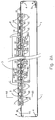
- Figures 2A , 3 , 4 , and 5 in combination illustrate the complete assembly of the preferred embodiment of a pair of air-to-vacuum-to-air (AVA) openings and the substrate transport system.
- the pair of AVA openings 2 facilitate the rapid transport of substrates from air into vacuum and then back into air.
- Figure 2A illustrates vacuum chamber 3, which is pumped to a suitable vacuum by known techniques.
- a pair of AVA openings 2 is shown on either side of the vacuum chamber 3.
- a pair of continuous metal strip belts 1 pass through both of the AVA openings 2 and also through the entire length of the vacuum chamber 3.
- a plurality of substrates 10, which are carried on the twin metal belts 1, are also shown.
- the AVA openings 2 are shown with a plurality of pockets 14 and a plurality of vacuum pump ports 15 for vacuum pumping.
- a pair of injection ports 11 are shown for the injection of process gas.
- a plurality of pulleys 4 are provided for moving the belts 1.
- a belt tensioner 9 maintains the belts 1 at a predetermined tension.
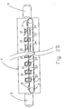
- FIG 3 shows the details of the AVA openings 2 in cross section.
- a top channel 2a and a bottom plate 2b are split by a belt bearing plate 20.
- parts 2a, 2b, and 20 form the cross section of the opening 2 of Figures 2A , 3 , and 4 .
- a clearance distance 21 on the order of 0.005 in. ⁇ 0.002 in. is formed around the substrate 10.
- This clearance distance 21 is formed between the substrate 10 and the top channel 2a and between the substrate 10 and the belt bearing plate 20.
- the clearance distance 21 is large enough so that the substrate 10 may move freely, but is small enough to provide resistance to fluid flow through the clearance distance 21. This resistance to fluid flow allows the vacuum chamber 3 to be maintained at a desired vacuum leveL
- the pair of continuous metal strip belts 1 provide a substrate carrier to convey the plurality of substrates 10.
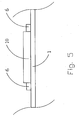
- Figure 5 is a detailed view of a pair of tabs 6 which are attached to the metal strip belt 1.
- the pair of continuous metal strip belts 1 provide a substrate carrier that will not be coated by the vacuum deposition processes.
- the elimination of coating on the belt 1 is a significant improvement over the prior art.
- the prior art utilized substrate carriers which enclosed the perimeter of the substrate in a "picture frame" type arrangement.
- the picture frame type substrate carriers are necessarily coated during deposition. These coatings lead to jamming in the close tolerance seals during motion, present occupational safety issues due to particle generation, and result in cross contamination between the processes. In the present invention, these problems have been addressed by exposing only the substrates 10 to coating during a vacuum deposition.
- the clearance distance 21 is not formed between the substrate carrier and the openings. Rather, the clearance distance 21 is formed between the precisely cut substrate 10 and the AVA openings 2. The clearance 21 is formed specifically between the substrate 10 and the top channel 2a and between the substrate 10 and the linear bearing plate 20.
- the use of the pair of metal strip belts 1 as the substrate carrier has many other advantages.
- the fact that the belts 1 have a low mass will create less wear on any bearing surface used.
- the low mass will also greatly decrease the inertia of the substrate carrier, thus allowing the substrate to be moved quickly between processing stations.
- Continuous metal strip belts 1 also have advantages in situations calling for a series of vacuum processes to be carried out in one vacuum chamber 3.
- Continuous metal strip belts 1 of 200 feet in length can be fabricated by known methods. This allows a large number of process steps to be carried out in one vacuum chamber 3.
- the present substrate carriers also facilitate scaling up the process. For larger substrates 10, the openings 2 must be increased in size. However, the strip belts 1 may be simply spaced further apart.
- the continuous metal strip belts 1 are preferably formed of metal alloys that have high resistance to corrosion and that retain high strength at elevated temperatures. These belts may be coated with other materials to alter the surface properties further, if needed. Many different attachments or tabs 6 for retaining the substrate 10 may be welded or fixed to the metal strip belts 1 at relatively low cost.
- a cut tolerance of ⁇ 0.003 inch is required for the glass substrates 10 which are carried on the continuous metal strip belts 1.
- High throughput, low cost equipment is commercially available for cutting the substrates 10 to the required tolerances.
- the precision glass cutting required for this invention is not an additional processing step, since the substrates 10 must be cut to size in any method.
- the continuous metal strip belts 1 are also relatively small in cross section.
- the small cross section decreases the thermal expansion as the belts pass through high temperature vacuum processes, which will decrease any tendency to jam in the AVA openings 2 due to thermal expansion.
- the relatively low mass of the metal strip belts 1 also allows the substrate carrier to cool and heat more rapidly than the prior art picture frame type substrate carrier.
- the low mass of the metal strip belts 1 allows the belt temperature to match the glass temperature during processing, thereby reducing thermal gradients in the glass substrates 10 which could otherwise lead to stresses that may crack the glass.
- the vacuum chamber 3 and a plurality of vacuum processing stations are illustrated in a partial schematic elevation view in section.
- the metal strip belts 1 carry the plurality of substrates 10 through the plurality of vacuum processing stations 200 and 300.
- the process stations 300 provide for cooling of substrates 10 by radiation to a pair of water cooled plates 34.
- Each of the process stations 200 of Figure 2A contain a pair of heated pockets 33.
- These heated pockets 33 provide a flux of heat or vapor and are suitably shaped blocks of a material with a high thermal conductivity.
- the pair of heated pockets 33 are shown with details of the pair of continuous metal strip belts 1 in cross section. Both upper and lower heated pockets 33 have a machined pocket 29.
- a deposition material 35 is shown in the pocket 29 of the lower heated pocket 33. Only the substrate 10 spans the pocket 29. No part of the belts 1 crosses the pocket 29, thus avoiding deposition anywhere but on the substrate 10.
- the upper heated pocket 33 serves as a heater for the substrate 10.
- Heated pocket 33 may be fabricated using any material which has an acceptable level of thermal conductivity. Further, that material should have a low level of porosity to prevent adsorption of air and water vapor and a low level of impurities.
- One material which has proven useful is purified pyrolitic grade graphite. However, metals and metals coated with ceramics, as well as other suitable materials, may be chosen.
- the heated pockets 33 are heated by a plurality of quartz halogen lamps 38, which are not damaged when used in vacuum at high temperatures.
- the temperature control of the heated pocket 33 may be accomplished by placing a thermocouple in the wall of the heated pocket 33 and using well known proportional with integral and derivative (PID) temperature control of the power to the lamps 38.
- Lamps 38 are contained in boxes 39 for protection. Boxes 39 also serve as support structure for the lamps 38 and the heated pocket 33.
- the boxes 39 also provide electrical isolation for safety, prevent arcing from the lamps 38, and also serve as radiation shields to reduce the loss of energy.
- Other means of heating the heated pocket 33 including resistive heating and inductive heating, for example, may be used as well.
- Each of the process stations 200 may perform a variety of processes on a substrate 10. These processes include: i) rapidly heating a substrate, ii) annealing a substrate and films, iii) thermally stripping a film from a substrate, iv) exposing a substrate and films to a vapor treatment, or v) depositing a thin film on a substrate.
- the chosen processes performed by station 200 depend on three parameters: a) the temperature of the lower heated pocket 33, b) the temperature of the upper heated pocket 33, and c) the presence or absence of the deposition material 35. For processes i) through iii) described above, no deposition material 35 is loaded into the pocket 29.
- the upper and lower heated pockets 33 are maintained at temperatures such that the rapid heating of glass substrates 10 may be done in a short cycle time, on the order of one minute.
- the uniformity of heating prevents cracking of the substrates 10.
- the upper and lower heated pocket 33 and substrate 10 are maintained at a temperature which will not resublime thin films off of the substrate 10.
- the upper and lower heated pocket 33 and substrate 10 are maintained at a temperature that is high enough to cause films on the substrate 10 to sublime away.
- deposition material 35 is loaded into the pocket 29.
- the upper heated pocket 33 and substrate 10 are maintained at a higher temperature than the lower heated pocket 33.
- the deposition material 35 will sublime in the pocket 29 of the lower heated pocket 33 and expose the lower surface of the substrate 10 to vapor, but the vapor will not be deposited as a film on the substrate 10.
- the lower heated pocket 33 is maintained at a relatively higher temperature than the substrate 10 and the upper heated pocket 33. In this manner, the deposition material 35 will sublime in the pocket 29 of the lower heated pocket 33, and the vapor will condense and be deposited as a film on the lower surface of the substrate 10. All of these processes are robust, may be performed at high throughput, are occupationally and environmentally safe, and involve low capital cost.
- the pair of metal belts 1 transports the substrates 10 through the plurality of process stations 200 or 300.
- the metal belts I and the substrates 10 may be moved continuously.
- the preferred embodiment of the present invention provides for intermittent motion of the metal belt 1 and the substrates 10. This motion is accomplished using a conventional stepper motor 7 and a stepper motor motion controller 8.
- the substrates 10 are placed at equal pitch distances on the belts 1, and the process stations 200 or 300 are placed one pitch distance apart.
- the intermittent motion consists of pauses in the motion of the belts 1 for processing and brief periods of motion of the belts 1 to advance the plurality of substrates 10 through the series of process steps. In this manner, an individual substrate 10 will pause at each process station 200 or 300 for an equal amount of time.
- a useful period of time hereinafter defined as the cycle time, consists of the total period of time for one pause and one movement of the belts 1.
- One substrate 10 will complete the series of inline vacuum process steps for each period of cycle time.
- process stations 200 or 300 are modular, a plurality of one type of process may be placed in series. If a given process step requires a processing time which exceeds the cycle time, then the given process step may be carried out over a series of similar processing stations 200 or 300. For example, an annealing step, which requires a longer period of time to complete than the cycle time, may be carried out over a series of annealing process stations 200.
- the deposition of thin films onto substrates 10 is a critical processing step of the present invention. A detailed description of the deposition apparatus is given below.
- the intermittent motion of the belts 1 allows a pause for deposition.
- the individual substrates 10, which are spaced at regular pitch intervals on the metal strip belts 1 will be in a sealing relationship with individual heated pockets 33.
- the individual heated pockets 33 will deposit a film onto the substrates 10.
- the thickness of the films can be varied by varying the temperature of each individual heated pocket 33. Closed loop control of film thickness may be achieved by measuring film thickness with known thickness monitors and adjusting the heated pocket 33 temperature as needed. Very precise control may be achieved since the deposition rate is a function of the temperature of the heated pocket 33.
- the present invention is specifically designed to produce very uniform film deposition across the surface of the substrate 10 at high throughput so that in a mass manufacturing environment the reproducibility of the film uniformity from one substrate 10 to another substrate 10 is tightly controlled over long periods of time.
- the substrate 10 is held in a novel sealing relationship with the pocket 29.
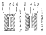
- Figure 6A and Figure 6B show an elevation view of two prior art devices used for film deposition by vacuum sublimation.
- the known method of Bozler in U.S. Patent 3,636,919 (1972 ) shows the source deposition material 35a and substrate 10a in an enclosed space.
- the enclosed space is formed by an upper heater 36 U and a lower heater 36 L. Because the substrate 10a is sealed in the enclosed space, the substrate 10a could not be moved and only one film could be deposited for each pump down of the vacuum chamber.
- Figure 6B details another known method according to Bonnet in U.S. Patent 5,304,499 (1994 ) which is commonly known as close spaced sublimation (CSS).
- CCS close spaced sublimation
- the deposition material 35a is placed on a flat heated plate 36 L and the substrate is held at a typical distance of 2 to 3 mm from the deposition material 35a.
- the disadvantage of this known method is that the clearance between the deposition material 35a and the substrate 10a forms a leak path for the vapor. This leak will lead to non-uniform deposition and the formation of toxic nano particles in the process space.
- the heated pocket deposition apparatus of the present invention overcomes the limitations of the prior art.
- Clearance distance 37 is formed on the two sides of the substrate 10 where the substrate 10 spans the belts 1.
- the clearance distance 37 is necessary to prevent the substrates 10 from touching the heated pocket 33 and damaging the deposited films.
- the clearance distance 37 is formed in such a manner as to provide a close tolerance slip fit seal between the top of the heated pocket 33 and the bottom of each of the substrates 10. Any vapor leak through the clearance distance 37 will be in the molecular flow regime and will be very small. This effectively eliminates vapor leaks through the clearance distance 37 and allows the substrates 10 to act as a shutter across the source pocket 29.
- the walls of the pocket 29 will collimate the vapor flux from the subliming material 35. Since the clearance distance 37 is at the top of the pocket 29 and at a right angle to the collimated vapor flux, nearly all of the vapor flux will pass the entry of the clearance distance 37 without directly entering it. Any vapor which does enter the clearance distance 37 due to gas scattering will be readily deposited on the surface of the substrate 10.
- the design of the clearance distance 37 allows for movement of multiple substrates 10 while maintaining a vapor seal. This design has advantages over the prior art since it will maintain the deposition uniformity across the substrate 10.
- the use of the substrates 10 to act as a shutter virtually eliminates cross contamination between heated pockets 33. The elimination of cross contamination allows the use of one vacuum boundary for the multiple processing steps and reduces the capital cost of the system. In most vacuum processes for processing PV devices, load locks or load locks in combination with intermediate chambers are used to prevent cross contamination between processing steps.
- the deposition material 35 must be distributed in an evenly spaced pattern across the floor of the pocket 29.
- the deposition material 35 may be in the form of powder, pellets pressed from powder, or random chunks. All of these forms of material for the fabrication of CdTe PV are commercially available.
- the distance between the deposition material 35 and the lower surface of the substrate 10, which is provided by the depth of the pocket 29 in the lower heated pocket 33, must be sufficient to allow for gas scattering of the sublimed species.
- Gas scattering is the result of collisions among the sublimed species or between the sublimed species and the molecules of the ambient background gas. These collisions deflect and scatter the sublimed species from following a straight line path from the deposition material 35 to the substrate 10. This scattering of the sublimed species results in a uniform deposition on the substrate 10
- the Knudsen number is a known dimensionless parameter which is used to quantify the amount of gas scattering present.
- the Knudsen number is the ratio of the mean free path in the pocket 29, at a given temperature and pressure, divided by the distance between the deposition material 35 and the substrate 10.
- the Knudsen number is less than 0.01, then the species within the pocket 29 are in viscous flow and gas scattering will be significant In this viscous flow regime, the gas scattering may lead to such a loss of energy from the sublimed species that they condense to form nano-particles.
- the species will be in a molecular flow regime with very little gas scattering. In this molecular flow regime, the sublimed species will travel in straight lines to the substrate. This line of sight deposition causes non-uniform film thickness across the substrate 10.
- the species will be in transition flow with some gas scattering. In the transition regime, the vapor flux is randomized by gas scattering.
- An additional advantage of the present invention is the heating of the process gas in the pocket 29. Since the substrates 10 act as a shutter for the heated pocket 33, the process gas in the source pocket 29 comes to a uniform high temperature. The high temperature of the process gas in the heated pocket 33 is another factor which prevents the formation of nano-particles due to the gas scattering collisions described above.
- the preferred embodiment of the present invention provides a means of forming a back electrode layer at high throughput and using equipment that is low capital cost. This layer is adherent to the other layers in the film stack and has a very low electrical resistivity.
- the back electrode is fabricated by a novel spray process at atmospheric pressure in process stations 52a and 52b.
- a layer of conductive graphite coating followed by a layer of conductive Ni coating are applied by known industrial spray methods to form the back electrode for carrying current. Sprays containing other metals besides Ni are known and may also be used.
- a metal conductive coating layer may also be applied by spray directly to the ohmic contact layer without an intervening carbon layer. In this description, carbon is not considered a metal.
- the gas used as a propellant in the spray process may be a dry inert gas such as N 2 or Ar, and the process may be performed in a controlled environment.
- the thick film of the back electrode contains a polymer binder, which provides a level of encapsulation and protection for the completed device.
- the spray is performed at room temperatures and does not harm or introduce defects into the previously fabricated semiconductor layers.
- the spray method has the advantage of low capital cost.
- the preferred embodiment of the present invention also provides a means of scribing that exhibits high throughput and low cost.
- a scribing step may be performed at the film scribing station 53a after the graphite layer is formed by the spray process at the process station 52a.
- the scribing is performed after the application of the graphite layer to prevent any damage to the semiconductor layers by handling.
- Figure 9A illustrates the details of the preferred embodiment of the film scribing method.
- a rotating wire brush 42 is brought into contact through openings 45 in a mask 41 to remove portions of the film 40 from the substrate 10.
- the openings 45 in the mask 41 are tapered in cross section and are narrower near the contact of the mask 41 and the film layers 40. This facilitates the entry of the rotating brush 42 into the openings 45.
- the mask 41 may be coated with a hard coating, such as titanium nitride, to reduce wear.
- the preferred embodiment of the film scribing method shown in Figure 9A does not require a precisely defined rotating brush 42 since the openings 45 in the mask 41 define the area of the film 40 which will be removed.
- the rotating wire brush 42 is passed axially along the openings 45 in the mask 41 over the substrate 10 to perform a scribe.
- a plurality of rotating metal brushes 42 may also be provided so that one pass along the axis of the openings 45 in the mask 41 will complete the plurality of scribes on an entire substrate 10.
- This film scribing method has the ability to scribe layers selectively. By using an abrasive powder with the rotating brush 42, the TCO layer may be scribed. By using the rotating brush 42 alone, all of the layers except the TCO layer may be removed.
- the process steps of the preferred embodiment of the present invention are shown in the flow chart of Figure 10A .
- the overall system 1000 required to perform the process is shown in Figure 1 .
- the apparatus required to perform the vacuum portion of the process, from step 2) of Figure 10A through step 12) of Figure 10A is illustrated in Figure 2A .
- the substrates 10 are transported through the vacuum process stations 200 and 300 on the metal strip belts 1.
- these process steps may be performed by a single one or a series of the vacuum process stations 200 or 300 illustrated in Figure 2A .
- the total time required for processing at each process station 200 or 300 and the transport of the substrate 10 to the next process station 200 or 300 is a unit of cycle time as defined above.
- the cycle time in the process description below is in the range of 30 seconds to 2 minutes.
- step (1) the substrate 10, which may have a TCO layer on one surface, is ultrasonically cleaned, rinsed, dipped in isopropyl alcohol to remove water from the surface, and dried in a clean room type mini-environment.
- step (2) the substrate 10 is transported into the vacuum chamber 3 through the AVA opening 2 using the metal strip belts 1.
- step (3) the substrate 10 is heated to a temperature in the range of 500° C to 560° C and transported to the next process.
- step (4) with the temperature of the substrate 10 in the range of 500° C to 560° C, a CdS film is deposited onto the TCO layer on the substrate 10 and the substrate 10 is transported to the next process.
- step (5) with the temperature of the substrate 10 in the range of 500° C to 560° C, a CdTe film is deposited onto the CdS layer on the substrate 10 and the substrate 10 is transported to the next process.
- step (6) and step (7) a CdCl 2 treatment is performed on the CdS/CdTe layers.
- step (6) with the temperature of the substrate 10 in the range of 300° C to 500° C, the CdS/CdTe layers on the substrate 10 are exposed to CdCl 2 and the substrate 10 is transported to the next process.
- the CdCl 2 exposure of the CdS/CdTe layers on the substrate 10 may be to a CdCl 2 vapor or a CdCl 2 film may be deposited on the CdTe layer. Either method of CdCl 2 exposure will produce high efficiency CdTe PV devices.
- a series of CdCl 2 treatment stations may be required.
- step (7) with the temperature of the substrate 10 in the range of 400° C to 450° C, the CdCl 2 treated layers on the substrate 10 are annealed, any CdCl 2 film is removed, and the substrate 10 is transported to the next process.
- a series of annealing stations may be required.
- step (6) and step (7) provide the CdCl 2 treatment of the CdS/CdTe layers.
- the CdCl 2 treatment of CdTe PV devices in vacuum is known.
- no prior art shows the CdCl 2 treatment step performed inline between the deposition of the CdTe layer and the formation of the ohmic contact layer and without the substrate leaving vacuum.
- no prior art shows directly transporting substrates from CdTe deposition to CdCl 2 treatment.
- step (8) the substrate 10 and films are cooled to the required temperature in the range of 25° C to 100° C and the substrate 10 is transported to the next process.
- a series of cooling stations may be required.
- step (9) and step (10) an ohmic low resistance contact is formed on the CdTe layer.
- step (9) with the substrate 10 temperature in a range of 150° C to 300° C°, a metal salt is deposited onto the CdTe layer on the substrate 10, and the substrate 10 is transported to the next process.
- One metal salt which has been used for this process step is CuCl.
- step (10) with the temperature of the substrate 10 in a range of 150° C to 250° C, the CdS/CdTe/metal salt layers on the substrate 10 are annealed, and the substrate 10 is transported to the next process. For this process step a series of annealing stations may be required.
- step (9) and step (10) produce a reaction between the metal salt and the surface of the CdTe layer and this reaction produces a thin p+ semiconductor layer on the CdTe surface to form the ohmic contact.
- a copper telluride such as Cu x Te or Cu doped CdTe:Cu or both may be formed.
- the thin p+ layer provides a low resistance ohmic contact on the surface of the CdTe layer and is stable.
- the prior art does not show the formation of an ohmic contact layer on CdTe by deposition of a metal salt onto the CdTe layer in vacuum.
- step (11) the substrate 10 and films are cooled to the required temperature in the range of 25° C to 100° C and the substrate 10 is transported to the next process.
- a series of cooling stations may be required.
- step (12) the substrate 10 is transported out of the vacuum chamber 3 through the AVA opening 2 on the metal strip belts 1.
- step (13) the ohmic contact layer is exposed to air for an optimum time in the range of 4 to 16 hours before a layer of conductive coating containing carbon is applied onto the ohmic contact layer by a spray process.
- the air exposure has led to PV devices with increased long term stability.
- a series of scribes in selected film layers on the substrate 10 are required to isolate individual PV cells on the substrate and to interconnect the individual cells on the substrate 10 to form a completed module.
- step (14) a plurality of first scribes through the all of the film layers on the substrate 10 including the transparent conductive oxide are performed.
- a second plurality of scribes through the carbon and the p/n layers without removing the TCO are performed parallel to the first set of scribes. Both of these sets of scribes are performed by the novel film scribing method described above with reference to Figure 9A .
- step (15) a layer of conductive coating containing Ni is applied by spray onto the layer of conductive coating containing carbon. Since the Ni metalization layer is formed after the second set of scribes, the Ni layer will fill the cuts in the semiconductor layers from the second scribe. This will cause an electrical connection of the back electrode of one cell to the front electrode of another cell. This step in combination with the following step of the final scribe of the metalization layer will complete the interconnection of the PV cells in series to form the PV module.
- step (16) a plurality of third scribes through only the metallization layers are performed.
- This third set of scribes is performed by the novel film scribing method described above with reference to Figure 9A .
- step (17) electrical connections are made and the finished module is encapsulated.
- any of the film deposition steps, including the steps 4), 5), 6), or 9) of Figure 10A more than one layer of a particular material may be deposited. These multiple layers may be deposited by a series of heated pocket deposition apparatuses. If one layer of material is deposited in a given cycle time, to a given thickness, then this single layer may be replaced by many thinner layers built up to the thickness of the single layer of material by using many depositions at shorter cycle times. Multiple depositions are advantageous since for every decrease in cycle time there is a corresponding increase in production rate. Multiple processing stations can also be used to decrease the cycle time for the other steps including annealing, vapor treatment, cooling, etc.
- a multijunction solar cell in accordance with the teachings of the present invention.
- a monolithic multijunction structure could be fabricated on the substrate.
- two or more solar cells would be stacked on one substrate in such a way that solar radiation passes through the larger band gap material first, and residual radiation passes through the stack to a smaller band gap material.
- the band gap of the materials needed could be tailored by using semiconductors formed by the combination of any of the elements Zn, Cd, Hg, S, Se, or Te. These elements are from group IIB and group VIB of the periodic table. These semiconductors may be in the form of alloys containing three or more elements.
- the multiple layers may be deposited by a series of heated pocket deposition apparatuses. Also, by varying the composition of the deposition material in the multiple heated pockets, a graded band gap photovoltaic device may be fabricated.
- the deposition of the metal compound may include compounds of Cu, Ag, Au, Hg, Sn, Sb, and Pb. These compounds may be metal salts as described in the preferred embodiment or organometallic compounds of Cu, Ag, Au, Hg, Sn, Sb, and Pb may also be used. These compounds may be deposited onto CdTe in vacuum to form an ohmic low resistance contact layer by reaction with the CdTe layer. This ohmic low resistance contact may be formed by tellurides of Cu, Ag, Au, Hg, Sn, Sb, and Pb, or the ohmic contact may be highly doped CdTe.
- An alternative embodiment to step 10) of Figure 10A is to anneal the ohmic contact layer in air, inert gas or other atmospheres outside the vacuum chamber.
- CdS and CdTe other semiconductors may be used instead of CdS and CdTe.
- These semiconductors are formed by the combination of any of the elements Zn, Cd, Hg, S, Se or, Te. These elements are from group IIB and group VIB of the periodic table. These semiconductors may also be in the form of alloys containing three or more elements.
- These compound semiconductors are known to be useful in the formation of PV devices, are readily sublimable, and may be deposited in vacuum by the present invention. A series of stations may be used to deposit the n-type and p-type semiconductors.
- more than one layer may be used to form the n-type and p-type regions of the device This allows a faster cycle time while still maintaining adequate semiconductor film thickness.
- the different stations may deposit different IIB-VIB compound semiconductors made up of the elements Zn, Cd, Hg, S, Se or, Te.
- halogen containing substances such as HCl or Cl 2 gas may be used in place of or in addition to CdCl 2 .
- a controlled amount of the gas can be introduced into the heated pocket 33.
- Other halogen containing substances which are known to have effects similar to CdCl 2 may also be used. Some known examples of these compounds are CdBr 2 and CdI 2 .
- a CdTe PV device may be fabricated without the deposition of CdS shown in step 4) of Figure 10A .
- the p/n junction is formed between the n-type TCO and the p-type CdTe or other IIB-VIB compounds.
- a CdTe device may be fabricated by depositing the CdS layer on the substrate 10 outside of the vacuum chamber 3 by known methods, including chemical bath deposition.
- the substrate 10 with the CdS layer would be brought into the vacuum chamber 3 and steps 3) through step 11) of Figure 10A would be performed in vacuum.
- a CdCl 2 treatment may be performed after step 4) CdS deposition and before step 5) CdTe deposition.
- This CdCl 2 treatment is in addition to the step 6) CdCl 2 treatment as shown in Figure 10A .
- the additional CdCl 2 treatment is known to further increase the device performance.
- the HPD deposition heated pocket 33 may be used to apply other film layers which would improve the performance of a CdS/CdTe PV device.
- One such layer is an anti-reflection (AR) coating which would be deposited on the glass substrate 10 on the opposite side of the substrate 10 from the TCO. The AR coating would face the sun and reduce the amount of incoming sunlight which is reflected off of the glass surface. This would increase the current that the device could produce.
- AR coating is a thin film of MgF 2 . Since MgF 2 is sublimable, this film may be applied with the heated pocket 33 deposition. The AR coating can be done at a suitable location in the vacuum chamber 3.
- i-SnO x Another layer which is known to increase the efficiency of a CdS/CdTe device is a layer of high resistivity intrinsic tin oxide (i-SnO x ).
- This layer would be applied between the TCO layer and the CdS layer or a layer of SnOx of the desired resistivity could be deposited directly on the glass substrate 10.
- This intrinsic layer has a much higher electrical resistivity than the TCO layer and has been shown to increase device efficiency.
- This resistive layer would allow the CdS layer to be thinner. The thinner CdS layer would allow more light to pass into the CdTe layer and increase the current the device would produce.
- the heated pocket 33 could be used to sublime i-SnO x .
- the i-SnO x deposition would be performed before the CdS deposition of step 4) of Figure 10A .
- step 15) of Figure 10A An alternate embodiment to step 15) of Figure 10A is that the graphite and Ni may be sprayed through a mask to form a patterned deposition. This patterned back electrode would eliminate the need for the second and third set of scribes shown in steps 14) and 16) of Figure 10A .
- a spray through a mask may also be used to fill the cut of the first scribe with an insulating compound before the spraying of the Ni conductive coating. The insulating compound eliminates electrical shunts between the Ni layer and the TCO.
- Figure 2B shows an alternate embodiment of the present invention in which the pair of continuous metal strip belts 1 are entirely contained within the vacuum chamber 3.
- a pair of known load locks 5 on either side of the chamber 3 provide a means of transporting the substrates 10 into and out of vacuum.
- FIG 7B illustrates an alternate embodiment of the vacuum process station of Figure 7A involving a different arrangement for the upper heated pocket 33.
- This alternate embodiment involves the addition of a baffle having a plurality of holes 28.
- the deposition material 35 is placed above the baffle in a confined space.
- the confined space has a lid 27, which may be removed to reload the deposition material 35.
- the vacuum process station 200 may be used as the heated pocket 33 to deposit films on the upper surface of the substrate 10.
- the substrates 10 can be transported by arrangements such as rollers, robotic arms, etc., which are well known. This would be especially useful for the deposition of the AR coating.
- FIG 8 illustrates an alternative to the heated pocket 33.
- This embodiment can be used to generate plasma in the pocket 29.
- This arrangement is called plasma enhanced heated pocket deposition (PEHPD).
- the alternate embodiment of the heated pocket 33 provides a high voltage pin 30 for the generation of plasma, the pin 30 may be made from graphite.
- the pin 30 is electrically isolated by insulation 31 which may be a quartz tube.
- the high voltage from the DC power supply 32 generates the plasma.
- the heated pocket-to-substrate distance in the PEHPD heated pocket must be large enough to produce ions within the pocket 29. If the pocket 29 is too shallow it will not produce a glow discharge at desirable pressures, when the substrate 10 is sealing the pocket 29 during deposition.
- both the CdS and CdTe heated pocket may optionally be of the PEHPD type so that the advantages of plasma enhanced deposition may be incorporated.
- These advantages of plasma enhanced deposition include: (i) doping of CdTe with nitrogen, (ii) passivation of the defects in CdTe. (iii) alteration of the morphology of CdS, (iv) doping of CdS, and (v) mixing of the CdS/CdTe interface.
- ZnTe may be doped with nitrogen by PEHPD to form ZnTe:N, a p+ semiconductor layer which may be used as an ohmic contact to CdTe.
- FIG 10B is a flow chart of the process steps of some of the alternate embodiments of the invention.
- the processing steps as shown schematically in that figure include (1) cleaning the substrate by known means in a clean room type mini-environment, (2) transporting the substrate into the vacuum chamber using AVA or load lock transport, (3) heating the substrate, (4) depositing a CdS film on the substrate using heated pockets with or without plasma, (5) depositing a CdTe film onto the CdS film using heated pockets with or without plasma, (6) performing a treatment, with a halogen containing substance, on the CdS/CdTe films using a heated pocket, (7) annealing the substrate and films, (8) forming an ohmic contact on the CdTe layer by heated pocket deposition of a Te layer on the CdTe layer or by heated pocket deposition with plasma of a ZnTe:N layer on the CdTe layer, (9) depositing a metallization layer onto the ohmic contact layer by heated pocket deposition of a sub
- Step 8) in Figure 10B illustrates another alternative embodiment of the present invention in which Te is used as an ohmic contact layer Te is easily sublimed and is known to form an ohmic contact material for CdTe devices.
- Te could be deposited inline by heated pocket deposition with or without a cooling step.
- a metal back electrode can be applied to the Te ohmic contact by either a vacuum deposition step or by the spray process of the present invention.
- Step 9) of Figure 10B illustrates an alternate embodiment of the present invention in which the back electrode metallization may be accomplished inline in vacuum.
- the back electrode metallization may be applied by a heated pocket deposition of metals including, but not limited to, Zn or Cd, which are readily sublimable and electrically conductive.
- Figure 9B illustrates an alternative embodiment of the scribing method of the present invention involving the use of an abrasive blast 43 which is provided by known methods.
- the abrasive blast 43 is performed through openings 45 in the mask 41 to remove portions of the film 40 from the substrate 10.
- This embodiment of the scribing method does not require a precisely defined abrasive blast 43 since the mask 41 defines the area of the film 40 which will be removed.
- the abrasive blast 43 is passed over the substrate 10 to perform a scribe.
- Each abrasive blast 43 may enter more than one opening 45 in the mask 41 so that one abrasive blast 43 may perform more than one scribe for each pass over the substrate 10.
- a plurality of abrasive blasts 43 may be provided so that one pass along the axis of the openings 45 in the mask 41 will complete the plurality of scribes of an entire substrate 10.
- Different abrasive media with different hardness and size may be provided so that various layers in the film stack 40 may be scribed selectively. This allows the scribing method of the present invention to: 1) scribe all the way through the film stack including the relatively hard TCO layer, and 2) selectively scribe through all of the layers above the TCO layer without removing the TCO.
Landscapes
- Photovoltaic Devices (AREA)
- Physical Deposition Of Substances That Are Components Of Semiconductor Devices (AREA)
- Physical Vapour Deposition (AREA)
Applications Claiming Priority (2)
| Application Number | Priority Date | Filing Date | Title |
|---|---|---|---|
| US583381 | 2000-05-30 | ||
| US09/583,381 US6423565B1 (en) | 2000-05-30 | 2000-05-30 | Apparatus and processes for the massproduction of photovotaic modules |
Publications (3)
| Publication Number | Publication Date |
|---|---|
| EP1160880A2 EP1160880A2 (en) | 2001-12-05 |
| EP1160880A3 EP1160880A3 (en) | 2005-12-07 |
| EP1160880B1 true EP1160880B1 (en) | 2012-07-11 |
Family
ID=24332883
Family Applications (1)
| Application Number | Title | Priority Date | Filing Date |
|---|---|---|---|
| EP01304749A Expired - Lifetime EP1160880B1 (en) | 2000-05-30 | 2001-05-30 | Process for the mass production of photovoltaic modules |
Country Status (3)
| Country | Link |
|---|---|
| US (3) | US6423565B1 (enExample) |
| EP (1) | EP1160880B1 (enExample) |
| JP (2) | JP4599503B2 (enExample) |
Cited By (2)
| Publication number | Priority date | Publication date | Assignee | Title |
|---|---|---|---|---|
| US20210351037A1 (en) * | 2018-10-05 | 2021-11-11 | Osram Opto Semiconductors Gmbh | Method for producing a semiconductor component comprising performing a plasma treatment, and semiconductor component |
| US20220406621A1 (en) * | 2021-06-17 | 2022-12-22 | Taiwan Semiconductor Manufacturing Co., Ltd. | Laser De-Bonding Carriers and Composite Carriers Thereof |
Families Citing this family (230)
| Publication number | Priority date | Publication date | Assignee | Title |
|---|---|---|---|---|
| US6423565B1 (en) * | 2000-05-30 | 2002-07-23 | Kurt L. Barth | Apparatus and processes for the massproduction of photovotaic modules |
| US6548751B2 (en) * | 2000-12-12 | 2003-04-15 | Solarflex Technologies, Inc. | Thin film flexible solar cell |
| JP3953742B2 (ja) * | 2001-03-14 | 2007-08-08 | 独立行政法人産業技術総合研究所 | 気体炭化水素の固定化材とその使用及び炭化水素の固形化方法 |
| CA2462590A1 (en) * | 2001-10-05 | 2003-04-17 | Solar Systems & Equipments S.R.L. | A process for large-scale production of cdte/cds thin film solar cells |
| JP4087172B2 (ja) * | 2002-07-11 | 2008-05-21 | セイコーインスツル株式会社 | 半導体装置の製造方法 |
| US8502064B2 (en) * | 2003-12-11 | 2013-08-06 | Philip Morris Usa Inc. | Hybrid system for generating power |
| SE0400582D0 (sv) * | 2004-03-05 | 2004-03-05 | Forskarpatent I Uppsala Ab | Method for in-line process control of the CIGS process |
| WO2005096396A1 (ja) * | 2004-03-31 | 2005-10-13 | Sanyo Electric Co., Ltd | 太陽電池の製造方法 |
| US7318769B2 (en) * | 2004-11-23 | 2008-01-15 | First Solar, Inc. | System and method for removing film from planar substrate peripheries |
| US20100186810A1 (en) * | 2005-02-08 | 2010-07-29 | Nicola Romeo | Method for the formation of a non-rectifying back-contact a cdte/cds thin film solar cell |
| ITLU20050002A1 (it) * | 2005-02-08 | 2006-08-09 | Solar Systems & Equipments Srl | UN NUOVO PROCESSO PER IL TRATTAMENTO IN AMBIENTE DI CLORO DELLE CELLE SOLARI A FILM SOTTILI DI CdTe/CdS senza l'uso di CdC12. |
| CN101163814A (zh) | 2005-03-18 | 2008-04-16 | 株式会社爱发科 | 成膜方法和成膜装置以及永磁铁和永磁铁的制造方法 |
| US7906722B2 (en) * | 2005-04-19 | 2011-03-15 | Palo Alto Research Center Incorporated | Concentrating solar collector with solid optical element |
| US20070079866A1 (en) * | 2005-10-07 | 2007-04-12 | Applied Materials, Inc. | System and method for making an improved thin film solar cell interconnect |
| US7799371B2 (en) * | 2005-11-17 | 2010-09-21 | Palo Alto Research Center Incorporated | Extruding/dispensing multiple materials to form high-aspect ratio extruded structures |
| US20070107773A1 (en) * | 2005-11-17 | 2007-05-17 | Palo Alto Research Center Incorporated | Bifacial cell with extruded gridline metallization |
| US7765949B2 (en) * | 2005-11-17 | 2010-08-03 | Palo Alto Research Center Incorporated | Extrusion/dispensing systems and methods |
| US20070227633A1 (en) * | 2006-04-04 | 2007-10-04 | Basol Bulent M | Composition control for roll-to-roll processed photovoltaic films |
| US7736913B2 (en) * | 2006-04-04 | 2010-06-15 | Solopower, Inc. | Composition control for photovoltaic thin film manufacturing |
| US7851693B2 (en) * | 2006-05-05 | 2010-12-14 | Palo Alto Research Center Incorporated | Passively cooled solar concentrating photovoltaic device |
| US8017860B2 (en) | 2006-05-15 | 2011-09-13 | Stion Corporation | Method and structure for thin film photovoltaic materials using bulk semiconductor materials |
| SE529315C2 (sv) * | 2006-05-24 | 2007-07-03 | Goeran Fajerson | Metod för tillverkning av fotovoltaiska celler och moduler från kiselskivor |
| US7803419B2 (en) * | 2006-09-22 | 2010-09-28 | Abound Solar, Inc. | Apparatus and method for rapid cooling of large area substrates in vacuum |
| US7922471B2 (en) | 2006-11-01 | 2011-04-12 | Palo Alto Research Center Incorporated | Extruded structure with equilibrium shape |
| US8226391B2 (en) * | 2006-11-01 | 2012-07-24 | Solarworld Innovations Gmbh | Micro-extrusion printhead nozzle with tapered cross-section |
| US8322025B2 (en) | 2006-11-01 | 2012-12-04 | Solarworld Innovations Gmbh | Apparatus for forming a plurality of high-aspect ratio gridline structures |
| US7780812B2 (en) * | 2006-11-01 | 2010-08-24 | Palo Alto Research Center Incorporated | Extrusion head with planarized edge surface |
| US20080116183A1 (en) * | 2006-11-21 | 2008-05-22 | Palo Alto Research Center Incorporated | Light Scanning Mechanism For Scan Displacement Invariant Laser Ablation Apparatus |
| US7928015B2 (en) * | 2006-12-12 | 2011-04-19 | Palo Alto Research Center Incorporated | Solar cell fabrication using extruded dopant-bearing materials |
| US7638438B2 (en) * | 2006-12-12 | 2009-12-29 | Palo Alto Research Center Incorporated | Solar cell fabrication using extrusion mask |
| US20080185039A1 (en) * | 2007-02-02 | 2008-08-07 | Hing Wah Chan | Conductor fabrication for optical element |
| US7767253B2 (en) * | 2007-03-09 | 2010-08-03 | Guardian Industries Corp. | Method of making a photovoltaic device with antireflective coating |
| US7954449B2 (en) * | 2007-05-08 | 2011-06-07 | Palo Alto Research Center Incorporated | Wiring-free, plumbing-free, cooled, vacuum chuck |
| US20080300918A1 (en) * | 2007-05-29 | 2008-12-04 | Commercenet Consortium, Inc. | System and method for facilitating hospital scheduling and support |
| US8071179B2 (en) | 2007-06-29 | 2011-12-06 | Stion Corporation | Methods for infusing one or more materials into nano-voids if nanoporous or nanostructured materials |
| US20100047954A1 (en) * | 2007-08-31 | 2010-02-25 | Su Tzay-Fa Jeff | Photovoltaic production line |
| KR20100051738A (ko) * | 2007-08-31 | 2010-05-17 | 어플라이드 머티어리얼스, 인코포레이티드 | 광전지 생산 라인 |
| US8759671B2 (en) | 2007-09-28 | 2014-06-24 | Stion Corporation | Thin film metal oxide bearing semiconductor material for single junction solar cell devices |
| US8287942B1 (en) | 2007-09-28 | 2012-10-16 | Stion Corporation | Method for manufacture of semiconductor bearing thin film material |
| US7998762B1 (en) | 2007-11-14 | 2011-08-16 | Stion Corporation | Method and system for large scale manufacture of thin film photovoltaic devices using multi-chamber configuration |
| WO2009091713A1 (en) * | 2008-01-15 | 2009-07-23 | First Solar, Inc. | System and method for depositing a material on a substrate |
| US8212139B2 (en) | 2008-01-18 | 2012-07-03 | Tenksolar, Inc. | Thin-film photovoltaic module |
| US8933320B2 (en) | 2008-01-18 | 2015-01-13 | Tenksolar, Inc. | Redundant electrical architecture for photovoltaic modules |
| US8748727B2 (en) | 2008-01-18 | 2014-06-10 | Tenksolar, Inc. | Flat-plate photovoltaic module |
| US8231431B2 (en) * | 2008-01-24 | 2012-07-31 | Applied Materials, Inc. | Solar panel edge deletion module |
| US20090188603A1 (en) * | 2008-01-25 | 2009-07-30 | Applied Materials, Inc. | Method and apparatus for controlling laminator temperature on a solar cell |
| CN102089892B (zh) * | 2008-02-27 | 2013-02-13 | 应用材料公司 | 用于在太阳能电池上形成电连接的设备与方法 |
| US7908743B2 (en) * | 2008-02-27 | 2011-03-22 | Applied Materials, Inc. | Method for forming an electrical connection |
| EP2257986A4 (en) * | 2008-03-04 | 2012-06-13 | Solexant Corp | PROCESS FOR THE MANUFACTURE OF SOLAR CELLS |
| US8410357B2 (en) * | 2008-03-18 | 2013-04-02 | Solexant Corp. | Back contact for thin film solar cells |
| US7858872B2 (en) * | 2008-03-18 | 2010-12-28 | Solexant Corp. | Back contact for thin film solar cells |
| EP2274456A1 (en) * | 2008-03-26 | 2011-01-19 | Solexant Corp. | Improved junctions in substrate solar cells |
| KR101073768B1 (ko) * | 2008-04-16 | 2011-10-13 | 내셔날 인스티튜트 오브 어드밴스드 인더스트리얼 사이언스 앤드 테크놀로지 | 카본 나노튜브 배향 집합체의 제조 장치 및 제조 방법 |
| EP2124264A1 (en) * | 2008-05-21 | 2009-11-25 | Applied Materials, Inc. | Method and apparatus for producing a solar cell module with integrated laser patterning |
| WO2009141411A1 (en) * | 2008-05-21 | 2009-11-26 | Applied Materials Inc. | Method and apparatus for producing a solar cell module with integrated laser patterning |
| US20090291231A1 (en) * | 2008-05-21 | 2009-11-26 | Applied Materials, Inc. | Method and apparatus for producing a solar cell module with integrated laser patterning |
| GB0809530D0 (en) * | 2008-05-27 | 2008-07-02 | Univ Durham | Improved physical vapour deposition processes |
| US8642138B2 (en) | 2008-06-11 | 2014-02-04 | Stion Corporation | Processing method for cleaning sulfur entities of contact regions |
| US8847249B2 (en) | 2008-06-16 | 2014-09-30 | Soraa, Inc. | Solid-state optical device having enhanced indium content in active regions |
| US9087943B2 (en) | 2008-06-25 | 2015-07-21 | Stion Corporation | High efficiency photovoltaic cell and manufacturing method free of metal disulfide barrier material |
| US8003432B2 (en) | 2008-06-25 | 2011-08-23 | Stion Corporation | Consumable adhesive layer for thin film photovoltaic material |
| US20100000589A1 (en) * | 2008-07-03 | 2010-01-07 | Amelio Solar, Inc. | Photovoltaic devices having conductive paths formed through the active photo absorber |
| US8767787B1 (en) | 2008-07-14 | 2014-07-01 | Soraa Laser Diode, Inc. | Integrated laser diodes with quality facets on GaN substrates |
| US8805134B1 (en) | 2012-02-17 | 2014-08-12 | Soraa Laser Diode, Inc. | Methods and apparatus for photonic integration in non-polar and semi-polar oriented wave-guided optical devices |
| US7981778B2 (en) * | 2009-07-22 | 2011-07-19 | Applied Materials, Inc. | Directional solid phase crystallization of thin amorphous silicon for solar cell applications |
| US8557045B2 (en) * | 2008-08-26 | 2013-10-15 | Colorado State University Research Foundation | Apparatus and method for fabricating photovoltaic modules using heated pocket deposition in a vacuum |
| EP2329518A2 (en) | 2008-08-26 | 2011-06-08 | Applied Materials, Inc. | Laser material removal methods and apparatus |
| US20100059115A1 (en) * | 2008-09-05 | 2010-03-11 | First Solar, Inc. | Coated Substrates and Semiconductor Devices Including the Substrates |
| US7999175B2 (en) | 2008-09-09 | 2011-08-16 | Palo Alto Research Center Incorporated | Interdigitated back contact silicon solar cells with laser ablated grooves |
| US7855089B2 (en) | 2008-09-10 | 2010-12-21 | Stion Corporation | Application specific solar cell and method for manufacture using thin film photovoltaic materials |
| US8394662B1 (en) | 2008-09-29 | 2013-03-12 | Stion Corporation | Chloride species surface treatment of thin film photovoltaic cell and manufacturing method |
| US8008110B1 (en) | 2008-09-29 | 2011-08-30 | Stion Corporation | Bulk sodium species treatment of thin film photovoltaic cell and manufacturing method |
| US8008112B1 (en) | 2008-09-29 | 2011-08-30 | Stion Corporation | Bulk chloride species treatment of thin film photovoltaic cell and manufacturing method |
| US8236597B1 (en) | 2008-09-29 | 2012-08-07 | Stion Corporation | Bulk metal species treatment of thin film photovoltaic cell and manufacturing method |
| US8026122B1 (en) | 2008-09-29 | 2011-09-27 | Stion Corporation | Metal species surface treatment of thin film photovoltaic cell and manufacturing method |
| US8476104B1 (en) | 2008-09-29 | 2013-07-02 | Stion Corporation | Sodium species surface treatment of thin film photovoltaic cell and manufacturing method |
| US8501521B1 (en) | 2008-09-29 | 2013-08-06 | Stion Corporation | Copper species surface treatment of thin film photovoltaic cell and manufacturing method |
| US7947524B2 (en) | 2008-09-30 | 2011-05-24 | Stion Corporation | Humidity control and method for thin film photovoltaic materials |
| US8383450B2 (en) | 2008-09-30 | 2013-02-26 | Stion Corporation | Large scale chemical bath system and method for cadmium sulfide processing of thin film photovoltaic materials |
| US7863074B2 (en) | 2008-09-30 | 2011-01-04 | Stion Corporation | Patterning electrode materials free from berm structures for thin film photovoltaic cells |
| US7910399B1 (en) | 2008-09-30 | 2011-03-22 | Stion Corporation | Thermal management and method for large scale processing of CIS and/or CIGS based thin films overlying glass substrates |
| US8425739B1 (en) | 2008-09-30 | 2013-04-23 | Stion Corporation | In chamber sodium doping process and system for large scale cigs based thin film photovoltaic materials |
| US8741689B2 (en) | 2008-10-01 | 2014-06-03 | Stion Corporation | Thermal pre-treatment process for soda lime glass substrate for thin film photovoltaic materials |
| US20110018103A1 (en) * | 2008-10-02 | 2011-01-27 | Stion Corporation | System and method for transferring substrates in large scale processing of cigs and/or cis devices |
| US8435826B1 (en) | 2008-10-06 | 2013-05-07 | Stion Corporation | Bulk sulfide species treatment of thin film photovoltaic cell and manufacturing method |
| US8003430B1 (en) | 2008-10-06 | 2011-08-23 | Stion Corporation | Sulfide species treatment of thin film photovoltaic cell and manufacturing method |
| US8168463B2 (en) | 2008-10-17 | 2012-05-01 | Stion Corporation | Zinc oxide film method and structure for CIGS cell |
| US20100118081A1 (en) * | 2008-11-07 | 2010-05-13 | Palo Alto Research Center Incorporated | Dead Volume Removal From An Extrusion Printhead |
| US20100117254A1 (en) * | 2008-11-07 | 2010-05-13 | Palo Alto Research Center Incorporated | Micro-Extrusion System With Airjet Assisted Bead Deflection |
| US8117983B2 (en) * | 2008-11-07 | 2012-02-21 | Solarworld Innovations Gmbh | Directional extruded bead control |
| US9150966B2 (en) * | 2008-11-14 | 2015-10-06 | Palo Alto Research Center Incorporated | Solar cell metallization using inline electroless plating |
| US8344243B2 (en) | 2008-11-20 | 2013-01-01 | Stion Corporation | Method and structure for thin film photovoltaic cell using similar material junction |
| US8080729B2 (en) * | 2008-11-24 | 2011-12-20 | Palo Alto Research Center Incorporated | Melt planarization of solar cell bus bars |
| US20100130014A1 (en) * | 2008-11-26 | 2010-05-27 | Palo Alto Research Center Incorporated | Texturing multicrystalline silicon |
| US8960120B2 (en) * | 2008-12-09 | 2015-02-24 | Palo Alto Research Center Incorporated | Micro-extrusion printhead with nozzle valves |
| US20100139756A1 (en) * | 2008-12-10 | 2010-06-10 | Palo Alto Research Center Incorporated | Simultaneously Writing Bus Bars And Gridlines For Solar Cell |
| US8563847B2 (en) | 2009-01-21 | 2013-10-22 | Tenksolar, Inc | Illumination agnostic solar panel |
| US20100206357A1 (en) * | 2009-02-18 | 2010-08-19 | Palo Alto Research Center Incorporated | Two-Part Solar Energy Collection System With Replaceable Solar Collector Component |
| US20100206356A1 (en) * | 2009-02-18 | 2010-08-19 | Palo Alto Research Center Incorporated | Rotational Trough Reflector Array For Solar-Electricity Generation |
| US20100206379A1 (en) * | 2009-02-18 | 2010-08-19 | Palo Alto Research Center Incorporated | Rotational Trough Reflector Array With Solid Optical Element For Solar-Electricity Generation |
| CN101820018B (zh) * | 2009-02-27 | 2014-12-17 | 比亚迪股份有限公司 | 一种CdS薄膜的制备方法 |
| EP3249699B1 (en) * | 2009-03-18 | 2020-04-15 | Evatec AG | Method of inline manufacturing a solar cell panel |
| US8837545B2 (en) | 2009-04-13 | 2014-09-16 | Soraa Laser Diode, Inc. | Optical device structure using GaN substrates and growth structures for laser applications |
| US8634442B1 (en) | 2009-04-13 | 2014-01-21 | Soraa Laser Diode, Inc. | Optical device structure using GaN substrates for laser applications |
| DE112010001615T5 (de) | 2009-04-13 | 2012-08-02 | Soraa, Inc. | Stuktur eines optischen Elements unter Verwendung von GaN-Substraten für Laseranwendungen |
| US8828776B2 (en) * | 2009-04-16 | 2014-09-09 | Tp Solar, Inc. | Diffusion furnaces employing ultra low mass transport systems and methods of wafer rapid diffusion processing |
| US20100273279A1 (en) * | 2009-04-27 | 2010-10-28 | Applied Materials, Inc. | Production line for the production of multiple sized photovoltaic devices |
| US8241943B1 (en) | 2009-05-08 | 2012-08-14 | Stion Corporation | Sodium doping method and system for shaped CIGS/CIS based thin film solar cells |
| US8372684B1 (en) | 2009-05-14 | 2013-02-12 | Stion Corporation | Method and system for selenization in fabricating CIGS/CIS solar cells |
| TW201101514A (en) * | 2009-05-18 | 2011-01-01 | First Solar Inc | Silicon nitride diffusion barrier layer for cadmium stannate TCO |
| US9829780B2 (en) | 2009-05-29 | 2017-11-28 | Soraa Laser Diode, Inc. | Laser light source for a vehicle |
| US10108079B2 (en) | 2009-05-29 | 2018-10-23 | Soraa Laser Diode, Inc. | Laser light source for a vehicle |
| US8247887B1 (en) | 2009-05-29 | 2012-08-21 | Soraa, Inc. | Method and surface morphology of non-polar gallium nitride containing substrates |
| US8427590B2 (en) | 2009-05-29 | 2013-04-23 | Soraa, Inc. | Laser based display method and system |
| US20100330711A1 (en) * | 2009-06-26 | 2010-12-30 | Applied Materials, Inc. | Method and apparatus for inspecting scribes in solar modules |
| US8507786B1 (en) | 2009-06-27 | 2013-08-13 | Stion Corporation | Manufacturing method for patterning CIGS/CIS solar cells |
| US8398772B1 (en) | 2009-08-18 | 2013-03-19 | Stion Corporation | Method and structure for processing thin film PV cells with improved temperature uniformity |
| US20110065227A1 (en) * | 2009-09-15 | 2011-03-17 | Applied Materials, Inc. | Common laser module for a photovoltaic production line |
| US8355418B2 (en) | 2009-09-17 | 2013-01-15 | Soraa, Inc. | Growth structures and method for forming laser diodes on {20-21} or off cut gallium and nitrogen containing substrates |
| US8750342B1 (en) | 2011-09-09 | 2014-06-10 | Soraa Laser Diode, Inc. | Laser diodes with scribe structures |
| TWI513016B (zh) * | 2009-09-22 | 2015-12-11 | First Solar Inc | 用以自基板之邊緣追蹤與移除塗層之系統及方法 |
| CN102696118A (zh) * | 2009-10-13 | 2012-09-26 | 第一太阳能有限公司 | 对碲化镉光伏器件进行退火的方法 |
| US20110083728A1 (en) * | 2009-10-14 | 2011-04-14 | Palo Alto Research Center Incorporated | Disordered Nanowire Solar Cell |
| US8227723B2 (en) * | 2009-10-19 | 2012-07-24 | Applied Materials, Inc. | Solder bonding method and apparatus |
| US8809096B1 (en) | 2009-10-22 | 2014-08-19 | Stion Corporation | Bell jar extraction tool method and apparatus for thin film photovoltaic materials |
| US20110104398A1 (en) * | 2009-10-29 | 2011-05-05 | General Electric Company | Method and system for depositing multiple materials on a substrate |
| US20110100419A1 (en) * | 2009-11-03 | 2011-05-05 | Palo Alto Research Center Incorporated | Linear Concentrating Solar Collector With Decentered Trough-Type Relectors |
| US20110143489A1 (en) * | 2009-12-11 | 2011-06-16 | General Electric Company | Process for making thin film solar cell |
| US20110139073A1 (en) * | 2009-12-15 | 2011-06-16 | Primestar Solar, Inc. | Conveyor assembly for a vapor deposition apparatus |
| US8187555B2 (en) * | 2009-12-15 | 2012-05-29 | Primestar Solar, Inc. | System for cadmium telluride (CdTe) reclamation in a vapor deposition conveyor assembly |
| US8189198B2 (en) * | 2009-12-15 | 2012-05-29 | Primestar Solar, Inc. | Active viewport detection assembly for substrate detection in a vapor detection system |
| US8481355B2 (en) * | 2009-12-15 | 2013-07-09 | Primestar Solar, Inc. | Modular system and process for continuous deposition of a thin film layer on a substrate |
| US8247255B2 (en) * | 2009-12-15 | 2012-08-21 | PrimeStar, Inc. | Modular system and process for continuous deposition of a thin film layer on a substrate |
| US8163089B2 (en) | 2009-12-16 | 2012-04-24 | Primestar Solar, Inc. | Vapor deposition apparatus and process for continuous deposition of a thin film layer on a substrate |
| US8039290B2 (en) * | 2009-12-16 | 2011-10-18 | General Electric Company | Method of making photovoltaic cell |
| US8430966B2 (en) * | 2009-12-16 | 2013-04-30 | Primestar Solar, Inc. | Vapor deposition apparatus and process for continuous deposition of a thin film layer on a substrate |
| US8748214B2 (en) | 2009-12-16 | 2014-06-10 | First Solar, Inc. | Method of p-type doping of cadmium telluride |
| US8430963B2 (en) * | 2010-01-07 | 2013-04-30 | Primestar Solar, Inc. | Cool-down system and method for a vapor deposition system |
| US8252117B2 (en) * | 2010-01-07 | 2012-08-28 | Primestar Solar, Inc. | Automatic feed system and related process for introducing source material to a thin film vapor deposition system |
| US8859880B2 (en) * | 2010-01-22 | 2014-10-14 | Stion Corporation | Method and structure for tiling industrial thin-film solar devices |
| US8263494B2 (en) | 2010-01-25 | 2012-09-11 | Stion Corporation | Method for improved patterning accuracy for thin film photovoltaic panels |
| US10147850B1 (en) | 2010-02-03 | 2018-12-04 | Soraa, Inc. | System and method for providing color light sources in proximity to predetermined wavelength conversion structures |
| US8905588B2 (en) | 2010-02-03 | 2014-12-09 | Sorra, Inc. | System and method for providing color light sources in proximity to predetermined wavelength conversion structures |
| DE102010008084A1 (de) * | 2010-02-15 | 2011-08-18 | Leybold Optics GmbH, 63755 | Vorrichtung zur thermischen Behandlung von Substraten |
| US9773933B2 (en) | 2010-02-23 | 2017-09-26 | Tenksolar, Inc. | Space and energy efficient photovoltaic array |
| US20110216401A1 (en) * | 2010-03-03 | 2011-09-08 | Palo Alto Research Center Incorporated | Scanning System With Orbiting Objective |
| US9096930B2 (en) | 2010-03-29 | 2015-08-04 | Stion Corporation | Apparatus for manufacturing thin film photovoltaic devices |
| US8142521B2 (en) * | 2010-03-29 | 2012-03-27 | Stion Corporation | Large scale MOCVD system for thin film photovoltaic devices |
| JP4977230B2 (ja) * | 2010-03-31 | 2012-07-18 | 積水化学工業株式会社 | エッチング方法及び装置 |
| US8480805B2 (en) * | 2010-04-16 | 2013-07-09 | Colorado State University Research Foundation | System and method for sealing a vapor deposition source |
| US8361229B2 (en) | 2010-04-22 | 2013-01-29 | Primestar Solar, Inc. | Seal configuration for a system for continuous deposition of a thin film layer on a substrate |
| US8252619B2 (en) * | 2010-04-23 | 2012-08-28 | Primestar Solar, Inc. | Treatment of thin film layers photovoltaic module manufacture |
| US8361232B2 (en) | 2010-04-29 | 2013-01-29 | Primestar Solar, Inc. | Vapor deposition apparatus and process for continuous indirect deposition of a thin film layer on a substrate |
| US8451876B1 (en) | 2010-05-17 | 2013-05-28 | Soraa, Inc. | Method and system for providing bidirectional light sources with broad spectrum |
| US9299861B2 (en) | 2010-06-15 | 2016-03-29 | Tenksolar, Inc. | Cell-to-grid redundandt photovoltaic system |
| US8236601B2 (en) | 2010-07-02 | 2012-08-07 | Primestar Solar, Inc. | Apparatus and methods of forming a conductive transparent oxide film layer for use in a cadmium telluride based thin film photovoltaic device |
| US8241938B2 (en) | 2010-07-02 | 2012-08-14 | Primestar Solar, Inc. | Methods of forming a conductive transparent oxide film layer for use in a cadmium telluride based thin film photovoltaic device |
| KR101454129B1 (ko) * | 2010-07-06 | 2014-10-22 | 가부시키가이샤 시마쓰세사쿠쇼 | 방사선 검출기의 제조 방법 |
| US8461061B2 (en) | 2010-07-23 | 2013-06-11 | Stion Corporation | Quartz boat method and apparatus for thin film thermal treatment |
| CN103155172B (zh) | 2010-08-10 | 2016-04-06 | 腾克太阳能公司 | 高效太阳能电池阵列 |
| DE102011008862A1 (de) * | 2010-09-04 | 2012-03-08 | Maschinenbau Gerold Gmbh & Co. Kg | Dünnschicht-Solarzelle sowie Anlage zur Herstellung von Dünnschicht-Solarzellen |
| US8628997B2 (en) | 2010-10-01 | 2014-01-14 | Stion Corporation | Method and device for cadmium-free solar cells |
| US7943415B1 (en) | 2010-10-27 | 2011-05-17 | Primestar Solar Inc. | Methods of sputtering cadmium sulfide layers for use in cadmium telluride based thin film photovoltaic devices |
| US7939363B1 (en) | 2010-10-27 | 2011-05-10 | General Electric Company | Systems and methods of intermixing cadmium sulfide layers and cadmium telluride layers for thin film photovoltaic devices |
| US8816319B1 (en) | 2010-11-05 | 2014-08-26 | Soraa Laser Diode, Inc. | Method of strain engineering and related optical device using a gallium and nitrogen containing active region |
| US9048170B2 (en) | 2010-11-09 | 2015-06-02 | Soraa Laser Diode, Inc. | Method of fabricating optical devices using laser treatment |
| US8975615B2 (en) * | 2010-11-09 | 2015-03-10 | Soraa Laser Diode, Inc. | Method of fabricating optical devices using laser treatment of contact regions of gallium and nitrogen containing material |
| US20120028393A1 (en) * | 2010-12-20 | 2012-02-02 | Primestar Solar, Inc. | Vapor deposition apparatus and process for continuous deposition of a doped thin film layer on a substrate |
| US20120052617A1 (en) | 2010-12-20 | 2012-03-01 | General Electric Company | Vapor deposition apparatus and process for continuous deposition of a doped thin film layer on a substrate |
| US20120027921A1 (en) | 2010-12-22 | 2012-02-02 | Primestar Solar, Inc. | Vapor deposition apparatus and process for continuous deposition of a thin film layer on a substrate |
| US8187386B2 (en) | 2010-12-22 | 2012-05-29 | Primestar Solar, Inc. | Temporally variable deposition rate of CdTe in apparatus and process for continuous deposition |
| US8801858B2 (en) | 2010-12-23 | 2014-08-12 | First Solar, Inc. | Non-wear shutter apparatus for a vapor deposition apparatus |
| US8771421B2 (en) | 2010-12-23 | 2014-07-08 | First Solar, Inc. | Entrance and exit roll seal configuration for a vapor deposition system |
| US8728200B1 (en) | 2011-01-14 | 2014-05-20 | Stion Corporation | Method and system for recycling processing gas for selenization of thin film photovoltaic materials |
| US8998606B2 (en) | 2011-01-14 | 2015-04-07 | Stion Corporation | Apparatus and method utilizing forced convection for uniform thermal treatment of thin film devices |
| US20120190180A1 (en) * | 2011-01-24 | 2012-07-26 | Lobue Joseph D | Thin film crystallization device and method for making a polycrystalline composition |
| US9025635B2 (en) | 2011-01-24 | 2015-05-05 | Soraa Laser Diode, Inc. | Laser package having multiple emitters configured on a support member |
| US9595813B2 (en) | 2011-01-24 | 2017-03-14 | Soraa Laser Diode, Inc. | Laser package having multiple emitters configured on a substrate member |
| US9093820B1 (en) | 2011-01-25 | 2015-07-28 | Soraa Laser Diode, Inc. | Method and structure for laser devices using optical blocking regions |
| DE202011110836U1 (de) * | 2011-02-21 | 2016-09-02 | Ctf Solar Gmbh | Vorrichtung zur Beschichtung von Substraten |
| US8962424B2 (en) | 2011-03-03 | 2015-02-24 | Palo Alto Research Center Incorporated | N-type silicon solar cell with contact/protection structures |
| US8247741B2 (en) | 2011-03-24 | 2012-08-21 | Primestar Solar, Inc. | Dynamic system for variable heating or cooling of linearly conveyed substrates |
| US9287684B2 (en) * | 2011-04-04 | 2016-03-15 | Soraa Laser Diode, Inc. | Laser package having multiple emitters with color wheel |
| US8241930B2 (en) | 2011-05-31 | 2012-08-14 | Primestar Solar, Inc. | Methods of forming a window layer in a cadmium telluride based thin film photovoltaic device |
| US8188562B2 (en) | 2011-05-31 | 2012-05-29 | Primestar Solar, Inc. | Multi-layer N-type stack for cadmium telluride based thin film photovoltaic devices and methods of making |
| US8247686B2 (en) | 2011-05-31 | 2012-08-21 | Primestar Solar, Inc. | Multi-layer N-type stack for cadmium telluride based thin film photovoltaic devices and methods of making |
| CN102244110B (zh) * | 2011-06-24 | 2012-09-05 | 四川大学 | 硒化钒薄膜作背接触层的CdTe太阳电池 |
| US8677932B2 (en) | 2011-08-03 | 2014-03-25 | First Solar, Inc. | Apparatus for metering granular source material in a thin film vapor deposition apparatus |
| US8436445B2 (en) | 2011-08-15 | 2013-05-07 | Stion Corporation | Method of manufacture of sodium doped CIGS/CIGSS absorber layers for high efficiency photovoltaic devices |
| US8822261B2 (en) * | 2011-09-26 | 2014-09-02 | First Solar, Inc. | Methods of making photovoltaic devices |
| JP5839321B2 (ja) * | 2011-09-29 | 2016-01-06 | 不二越機械工業株式会社 | インゴットへの切り代プレートおよび取付プレートの接着方法および接着装置 |
| US8673777B2 (en) | 2011-09-30 | 2014-03-18 | First Solar, Inc. | In-line deposition system and process for deposition of a thin film layer |
| US8722136B2 (en) * | 2011-10-21 | 2014-05-13 | First Solar, Inc. | Heat strengthening of a glass superstrate for thin film photovoltaic devices |
| NL2007658C2 (nl) * | 2011-10-26 | 2013-05-01 | Smit Ovens Bv | Inrichting voor het verhitten van een substraat. |
| US20130115372A1 (en) | 2011-11-08 | 2013-05-09 | Primestar Solar, Inc. | High emissivity distribution plate in vapor deposition apparatus and processes |
| CN104025252B (zh) * | 2011-11-18 | 2018-04-06 | 第一太阳能有限公司 | 提供用于光伏模块的单步骤氯化镉蒸气处理的方法和设备 |
| US20130140135A1 (en) * | 2011-12-02 | 2013-06-06 | Lian Hok Tan | Belt conveyor for conveying solar wafers during fabrication |
| CN104066867B (zh) * | 2011-12-30 | 2017-10-17 | Hoya株式会社 | 光学元件、光学薄膜形成装置及光学薄膜形成方法 |
| US9054245B2 (en) | 2012-03-02 | 2015-06-09 | First Solar, Inc. | Doping an absorber layer of a photovoltaic device via diffusion from a window layer |
| US9020003B1 (en) | 2012-03-14 | 2015-04-28 | Soraa Laser Diode, Inc. | Group III-nitride laser diode grown on a semi-polar orientation of gallium and nitrogen containing substrates |
| US9343871B1 (en) | 2012-04-05 | 2016-05-17 | Soraa Laser Diode, Inc. | Facet on a gallium and nitrogen containing laser diode |
| CN102628164B (zh) * | 2012-04-27 | 2013-06-12 | 保定天威薄膜光伏有限公司 | 一种控制太阳能电池组件电学性能低下及外观缺陷的方法 |
| US9034686B2 (en) * | 2012-06-29 | 2015-05-19 | First Solar, Inc. | Manufacturing methods for semiconductor devices |
| US9324898B2 (en) | 2012-09-25 | 2016-04-26 | Alliance For Sustainable Energy, Llc | Varying cadmium telluride growth temperature during deposition to increase solar cell reliability |
| CN102881778B (zh) * | 2012-10-17 | 2015-01-28 | 上海太阳能电池研究与发展中心 | 一种CdTe薄膜电池的热处理方法 |
| US20150027372A1 (en) * | 2013-07-26 | 2015-01-29 | First Solar, Inc. | Vapor Deposition Apparatus for Continuous Deposition of Multiple Thin Film Layers on a Substrate |
| US9093599B2 (en) | 2013-07-26 | 2015-07-28 | First Solar, Inc. | Vapor deposition apparatus for continuous deposition of multiple thin film layers on a substrate |
| CN104425652B (zh) | 2013-08-30 | 2019-04-05 | 中国建材国际工程集团有限公司 | 用于生产薄膜太阳能电池的方法 |
| KR20150078549A (ko) * | 2013-12-31 | 2015-07-08 | 한국과학기술원 | 집적형 박막 태양전지의 제조 장치 |
| US11437774B2 (en) | 2015-08-19 | 2022-09-06 | Kyocera Sld Laser, Inc. | High-luminous flux laser-based white light source |
| US9787963B2 (en) | 2015-10-08 | 2017-10-10 | Soraa Laser Diode, Inc. | Laser lighting having selective resolution |
| EP3387679B1 (en) | 2015-12-09 | 2022-04-27 | First Solar, Inc. | Photovoltaic devices and method of manufacturing |
| DE102016101856B4 (de) | 2016-02-03 | 2017-11-30 | Ctf Solar Gmbh | Verfahren zum Abscheiden einer CdTe-Schicht auf einem Substrat |
| TW201812887A (zh) * | 2016-09-23 | 2018-04-01 | 頎邦科技股份有限公司 | 晶圓切割方法 |
| US20180127875A1 (en) * | 2016-11-04 | 2018-05-10 | National Chung Shan Institute Of Science And Technology | Apparatus for performing selenization and sulfurization process on glass substrate |
| JP6316920B1 (ja) * | 2016-12-07 | 2018-04-25 | 國家中山科學研究院 | ガラス基板のセレン化及び硫化工程に用いる設備 |
| JP6618459B2 (ja) * | 2016-12-26 | 2019-12-11 | 東芝三菱電機産業システム株式会社 | 薄膜製造装置及び薄膜製造方法 |
| US10771155B2 (en) | 2017-09-28 | 2020-09-08 | Soraa Laser Diode, Inc. | Intelligent visible light with a gallium and nitrogen containing laser source |
| EP3717675B1 (en) * | 2017-12-01 | 2022-09-21 | China Triumph International Engineering Co., Ltd. | Physical vapor deposition system comprising positioning marker and method for adjusting distance between crucible and substrate |
| US10222474B1 (en) | 2017-12-13 | 2019-03-05 | Soraa Laser Diode, Inc. | Lidar systems including a gallium and nitrogen containing laser light source |
| US10551728B1 (en) | 2018-04-10 | 2020-02-04 | Soraa Laser Diode, Inc. | Structured phosphors for dynamic lighting |
| US11239637B2 (en) | 2018-12-21 | 2022-02-01 | Kyocera Sld Laser, Inc. | Fiber delivered laser induced white light system |
| US11421843B2 (en) | 2018-12-21 | 2022-08-23 | Kyocera Sld Laser, Inc. | Fiber-delivered laser-induced dynamic light system |
| US12000552B2 (en) | 2019-01-18 | 2024-06-04 | Kyocera Sld Laser, Inc. | Laser-based fiber-coupled white light system for a vehicle |
| US12152742B2 (en) | 2019-01-18 | 2024-11-26 | Kyocera Sld Laser, Inc. | Laser-based light guide-coupled wide-spectrum light system |
| US11884202B2 (en) | 2019-01-18 | 2024-01-30 | Kyocera Sld Laser, Inc. | Laser-based fiber-coupled white light system |
| GB2589356A (en) * | 2019-11-28 | 2021-06-02 | Univ Exeter | Van der Waals heterostructures |
| KR102871322B1 (ko) * | 2021-03-23 | 2025-10-16 | 주성엔지니어링(주) | 기판처리장치 |
| CN114005905B (zh) * | 2021-10-22 | 2023-10-17 | 成都中建材光电材料有限公司 | 一种碲化镉太阳能电池的连续生产装备 |
| CN117832333B (zh) * | 2024-03-05 | 2024-05-31 | 龙焱能源科技(杭州)有限公司 | 一种碲化镉薄膜电池及其制备方法 |
Family Cites Families (24)
| Publication number | Priority date | Publication date | Assignee | Title |
|---|---|---|---|---|
| US3636919A (en) | 1969-12-02 | 1972-01-25 | Univ Ohio State | Apparatus for growing films |
| US3294670A (en) | 1963-10-07 | 1966-12-27 | Western Electric Co | Apparatus for processing materials in a controlled atmosphere |
| US3787961A (en) * | 1972-06-19 | 1974-01-29 | Matsuo Electric Co | Chip-shaped, non-polarized solid state electrolytic capacitor and method of making same |
| US4017773A (en) * | 1975-05-27 | 1977-04-12 | Sprague Electric Company | Solid valve-metal capacitor with buried graphite in the particles in the electrolyte |
| US4319069A (en) | 1980-07-25 | 1982-03-09 | Eastman Kodak Company | Semiconductor devices having improved low-resistance contacts to p-type CdTe, and method of preparation |
| GB2084197B (en) | 1980-09-23 | 1984-02-22 | Univ Delaware | Deposition material by vacuum evaporation |
| US4336285A (en) * | 1981-02-03 | 1982-06-22 | Radiation Monitoring Devices, Inc. | Method to synthesize and produce thin films by spray pyrolysis |
| JPS6028136B2 (ja) * | 1981-10-14 | 1985-07-03 | 株式会社日立製作所 | 炉心管 |
| JPS6149483A (ja) | 1984-08-17 | 1986-03-11 | Matsushita Electric Ind Co Ltd | 光導電性薄膜の製造方法 |
| US4798660A (en) | 1985-07-16 | 1989-01-17 | Atlantic Richfield Company | Method for forming Cu In Se2 films |
| US4734381A (en) | 1985-10-24 | 1988-03-29 | Atlantic Richfield Company | Method of making a thin film cadmium telluride solar cell |
| DE4132882C2 (de) | 1991-10-03 | 1996-05-09 | Antec Angewandte Neue Technolo | Verfahren zur Herstellung von pn CdTe/CdS-Dünnschichtsolarzellen |
| GB9123684D0 (en) | 1991-11-07 | 1992-01-02 | Bp Solar Ltd | Ohmic contacts |
| US5501744A (en) | 1992-01-13 | 1996-03-26 | Photon Energy, Inc. | Photovoltaic cell having a p-type polycrystalline layer with large crystals |
| JPH05291599A (ja) * | 1992-04-09 | 1993-11-05 | Matsushita Electric Ind Co Ltd | 太陽電池の製造法 |
| US5248349A (en) | 1992-05-12 | 1993-09-28 | Solar Cells, Inc. | Process for making photovoltaic devices and resultant product |
| US5393675A (en) | 1993-05-10 | 1995-02-28 | The University Of Toledo | Process for RF sputtering of cadmium telluride photovoltaic cell |
| JPH07115216A (ja) * | 1993-10-18 | 1995-05-02 | Matsushita Electric Ind Co Ltd | 太陽電池の製造方法 |
| JPH0878355A (ja) * | 1994-09-05 | 1996-03-22 | Japan Energy Corp | 化合物半導体のオーミック電極及びその製造方法 |
| EP0744779A3 (en) | 1995-05-17 | 1998-10-21 | Matsushita Battery Industrial Co Ltd | A manufacturing method of compound semiconductor thinfilms and photoelectric device or solar cell using the same compound semiconductor thinfilms |
| WO1997021252A1 (en) * | 1995-12-07 | 1997-06-12 | Japan Energy Corporation | Method of producing photoelectric conversion device |
| DE19903798A1 (de) * | 1999-02-01 | 2000-08-10 | Angew Solarenergie Ase Gmbh | Verfahren und Anordnung zur Wärmebehandlung von flächigen Gegenständen |
| US6251701B1 (en) * | 2000-03-01 | 2001-06-26 | The United States Of America As Represented By The United States Department Of Energy | All-vapor processing of p-type tellurium-containing II-VI semiconductor and ohmic contacts thereof |
| US6423565B1 (en) * | 2000-05-30 | 2002-07-23 | Kurt L. Barth | Apparatus and processes for the massproduction of photovotaic modules |
-
2000
- 2000-05-30 US US09/583,381 patent/US6423565B1/en not_active Expired - Lifetime
-
2001
- 2001-05-29 JP JP2001160953A patent/JP4599503B2/ja not_active Expired - Fee Related
- 2001-05-30 EP EP01304749A patent/EP1160880B1/en not_active Expired - Lifetime
-
2002
- 2002-07-22 US US10/200,265 patent/US20030129810A1/en not_active Abandoned
-
2004
- 2004-03-24 US US10/808,050 patent/US7220321B2/en not_active Expired - Fee Related
-
2010
- 2010-01-20 JP JP2010010341A patent/JP2010141343A/ja active Pending
Non-Patent Citations (3)
| Title |
|---|
| DEBBAGH F. ET AL: "Some annealing effects on r.f. sputtered Cu/Te/CdTe structure", MATERIALS SCIENCE AND ENGINEERING B, vol. 38, 4 January 1996 (1996-01-04), ELSEVIER, LAUSANNE, CH, pages 223 - 227, XP004017605 * |
| MCCANDLESS B.E. ET AL: "Influence of processing conditions on performance and stability in polycrystalline thin-film CdTe-based solar cells", AIP CONF. PROC., vol. 462, 5 March 1999 (1999-03-05), pages 182 - 187 * |
| ROMEO N. ET AL: "Back contacts to CSS CdS/CdTe solar cells and stability of performances", THIN SOLID FILMS, vol. 361-362, 1 February 2000 (2000-02-01), pages 327 - 329, XP004187495 * |
Cited By (4)
| Publication number | Priority date | Publication date | Assignee | Title |
|---|---|---|---|---|
| US20210351037A1 (en) * | 2018-10-05 | 2021-11-11 | Osram Opto Semiconductors Gmbh | Method for producing a semiconductor component comprising performing a plasma treatment, and semiconductor component |
| US11915935B2 (en) * | 2018-10-05 | 2024-02-27 | Osram Opto Semiconductors Gmbh | Method for producing a semiconductor component comprising performing a plasma treatment, and semiconductor component |
| US20220406621A1 (en) * | 2021-06-17 | 2022-12-22 | Taiwan Semiconductor Manufacturing Co., Ltd. | Laser De-Bonding Carriers and Composite Carriers Thereof |
| US11908708B2 (en) * | 2021-06-17 | 2024-02-20 | Taiwan Semiconductor Manufacturing Co., Ltd. | Laser de-bonding carriers and composite carriers thereof |
Also Published As
| Publication number | Publication date |
|---|---|
| US20050158891A1 (en) | 2005-07-21 |
| EP1160880A3 (en) | 2005-12-07 |
| JP4599503B2 (ja) | 2010-12-15 |
| US6423565B1 (en) | 2002-07-23 |
| US20030129810A1 (en) | 2003-07-10 |
| JP2010141343A (ja) | 2010-06-24 |
| JP2002064215A (ja) | 2002-02-28 |
| EP1160880A2 (en) | 2001-12-05 |
| US7220321B2 (en) | 2007-05-22 |
Similar Documents
| Publication | Publication Date | Title |
|---|---|---|
| EP1160880B1 (en) | Process for the mass production of photovoltaic modules | |
| US8557045B2 (en) | Apparatus and method for fabricating photovoltaic modules using heated pocket deposition in a vacuum | |
| US7838763B2 (en) | Manufacturing apparatus and method for large-scale production of thin-film solar cells | |
| EP2381485B1 (en) | Treatment of thin film layers photovoltaic module | |
| US8349084B2 (en) | Apparatus and systems for intermixing cadmium sulfide layers and cadmium telluride layers for thin film photovoltaic devices | |
| EP1424735B1 (en) | Method for forming light-absorbing layer | |
| US20120024695A1 (en) | Systems and methods for high-rate deposition of thin film layers on photovoltaic module substrates | |
| US20110266141A1 (en) | System and methods for high-rate co-sputtering of thin film layers on photovoltaic module substrates | |
| EP2381012A1 (en) | Modular system for high-rate deposition of thin film layers on photovoltaic module substrates | |
| EP2381010B1 (en) | Methods for high-rate sputtering of a compound semiconductor on large area substrates | |
| EP2402483B1 (en) | Apparatus and method for isolating a viewport |
Legal Events
| Date | Code | Title | Description |
|---|---|---|---|
| PUAI | Public reference made under article 153(3) epc to a published international application that has entered the european phase |
Free format text: ORIGINAL CODE: 0009012 |
|
| AK | Designated contracting states |
Kind code of ref document: A2 Designated state(s): AT BE CH CY DE DK ES FI FR GB GR IE IT LI LU MC NL PT SE TR |
|
| AX | Request for extension of the european patent |
Free format text: AL;LT;LV;MK;RO;SI |
|
| PUAL | Search report despatched |
Free format text: ORIGINAL CODE: 0009013 |
|
| AK | Designated contracting states |
Kind code of ref document: A3 Designated state(s): AT BE CH CY DE DK ES FI FR GB GR IE IT LI LU MC NL PT SE TR |
|
| AX | Request for extension of the european patent |
Extension state: AL LT LV MK RO SI |
|
| 17P | Request for examination filed |
Effective date: 20060606 |
|
| AKX | Designation fees paid |
Designated state(s): AT BE CH CY DE DK ES FI FR GB GR IE IT LI LU MC NL PT SE TR |
|
| 17Q | First examination report despatched |
Effective date: 20060810 |
|
| RAP1 | Party data changed (applicant data changed or rights of an application transferred) |
Owner name: ABOUND SOLAR, INC. |
|
| RIN1 | Information on inventor provided before grant (corrected) |
Inventor name: SAMPATH, WALAJABAD S. Inventor name: ENZENROTH, ROBERT A. Inventor name: BARTH, KURT L. |
|
| GRAP | Despatch of communication of intention to grant a patent |
Free format text: ORIGINAL CODE: EPIDOSNIGR1 |
|
| RIC1 | Information provided on ipc code assigned before grant |
Ipc: H01L 31/18 20060101AFI20120123BHEP |
|
| RTI1 | Title (correction) |
Free format text: PROCESS FOR THE MASS PRODUCTION OF PHOTOVOLTAIC MODULES |
|
| GRAS | Grant fee paid |
Free format text: ORIGINAL CODE: EPIDOSNIGR3 |
|
| GRAA | (expected) grant |
Free format text: ORIGINAL CODE: 0009210 |
|
| AK | Designated contracting states |
Kind code of ref document: B1 Designated state(s): AT BE CH CY DE DK ES FI FR GB GR IE IT LI LU MC NL PT SE TR |
|
| REG | Reference to a national code |
Ref country code: GB Ref legal event code: FG4D |
|
| REG | Reference to a national code |
Ref country code: CH Ref legal event code: EP |
|
| REG | Reference to a national code |
Ref country code: AT Ref legal event code: REF Ref document number: 566510 Country of ref document: AT Kind code of ref document: T Effective date: 20120715 |
|
| REG | Reference to a national code |
Ref country code: IE Ref legal event code: FG4D |
|
| REG | Reference to a national code |
Ref country code: DE Ref legal event code: R096 Ref document number: 60146802 Country of ref document: DE Effective date: 20120906 |
|
| REG | Reference to a national code |
Ref country code: NL Ref legal event code: VDEP Effective date: 20120711 |
|
| REG | Reference to a national code |
Ref country code: AT Ref legal event code: MK05 Ref document number: 566510 Country of ref document: AT Kind code of ref document: T Effective date: 20120711 |
|
| PG25 | Lapsed in a contracting state [announced via postgrant information from national office to epo] |
Ref country code: BE Free format text: LAPSE BECAUSE OF FAILURE TO SUBMIT A TRANSLATION OF THE DESCRIPTION OR TO PAY THE FEE WITHIN THE PRESCRIBED TIME-LIMIT Effective date: 20120711 Ref country code: FI Free format text: LAPSE BECAUSE OF FAILURE TO SUBMIT A TRANSLATION OF THE DESCRIPTION OR TO PAY THE FEE WITHIN THE PRESCRIBED TIME-LIMIT Effective date: 20120711 Ref country code: AT Free format text: LAPSE BECAUSE OF FAILURE TO SUBMIT A TRANSLATION OF THE DESCRIPTION OR TO PAY THE FEE WITHIN THE PRESCRIBED TIME-LIMIT Effective date: 20120711 Ref country code: CY Free format text: LAPSE BECAUSE OF FAILURE TO SUBMIT A TRANSLATION OF THE DESCRIPTION OR TO PAY THE FEE WITHIN THE PRESCRIBED TIME-LIMIT Effective date: 20120711 |
|
| PG25 | Lapsed in a contracting state [announced via postgrant information from national office to epo] |
Ref country code: SE Free format text: LAPSE BECAUSE OF FAILURE TO SUBMIT A TRANSLATION OF THE DESCRIPTION OR TO PAY THE FEE WITHIN THE PRESCRIBED TIME-LIMIT Effective date: 20120711 Ref country code: GR Free format text: LAPSE BECAUSE OF FAILURE TO SUBMIT A TRANSLATION OF THE DESCRIPTION OR TO PAY THE FEE WITHIN THE PRESCRIBED TIME-LIMIT Effective date: 20121012 Ref country code: PT Free format text: LAPSE BECAUSE OF FAILURE TO SUBMIT A TRANSLATION OF THE DESCRIPTION OR TO PAY THE FEE WITHIN THE PRESCRIBED TIME-LIMIT Effective date: 20121112 |
|
| PG25 | Lapsed in a contracting state [announced via postgrant information from national office to epo] |
Ref country code: NL Free format text: LAPSE BECAUSE OF FAILURE TO SUBMIT A TRANSLATION OF THE DESCRIPTION OR TO PAY THE FEE WITHIN THE PRESCRIBED TIME-LIMIT Effective date: 20120711 |
|
| PG25 | Lapsed in a contracting state [announced via postgrant information from national office to epo] |
Ref country code: DK Free format text: LAPSE BECAUSE OF FAILURE TO SUBMIT A TRANSLATION OF THE DESCRIPTION OR TO PAY THE FEE WITHIN THE PRESCRIBED TIME-LIMIT Effective date: 20120711 Ref country code: ES Free format text: LAPSE BECAUSE OF FAILURE TO SUBMIT A TRANSLATION OF THE DESCRIPTION OR TO PAY THE FEE WITHIN THE PRESCRIBED TIME-LIMIT Effective date: 20121022 |
|
| PLBE | No opposition filed within time limit |
Free format text: ORIGINAL CODE: 0009261 |
|
| STAA | Information on the status of an ep patent application or granted ep patent |
Free format text: STATUS: NO OPPOSITION FILED WITHIN TIME LIMIT |
|
| PG25 | Lapsed in a contracting state [announced via postgrant information from national office to epo] |
Ref country code: IT Free format text: LAPSE BECAUSE OF FAILURE TO SUBMIT A TRANSLATION OF THE DESCRIPTION OR TO PAY THE FEE WITHIN THE PRESCRIBED TIME-LIMIT Effective date: 20120711 |
|
| 26N | No opposition filed |
Effective date: 20130412 |
|
| REG | Reference to a national code |
Ref country code: DE Ref legal event code: R097 Ref document number: 60146802 Country of ref document: DE Effective date: 20130412 |
|
| PG25 | Lapsed in a contracting state [announced via postgrant information from national office to epo] |
Ref country code: MC Free format text: LAPSE BECAUSE OF FAILURE TO SUBMIT A TRANSLATION OF THE DESCRIPTION OR TO PAY THE FEE WITHIN THE PRESCRIBED TIME-LIMIT Effective date: 20120711 |
|
| REG | Reference to a national code |
Ref country code: CH Ref legal event code: PL |
|
| GBPC | Gb: european patent ceased through non-payment of renewal fee |
Effective date: 20130530 |
|
| PG25 | Lapsed in a contracting state [announced via postgrant information from national office to epo] |
Ref country code: CH Free format text: LAPSE BECAUSE OF NON-PAYMENT OF DUE FEES Effective date: 20130531 Ref country code: DE Free format text: LAPSE BECAUSE OF NON-PAYMENT OF DUE FEES Effective date: 20131203 Ref country code: LI Free format text: LAPSE BECAUSE OF NON-PAYMENT OF DUE FEES Effective date: 20130531 |
|
| REG | Reference to a national code |
Ref country code: IE Ref legal event code: MM4A |
|
| REG | Reference to a national code |
Ref country code: DE Ref legal event code: R119 Ref document number: 60146802 Country of ref document: DE Effective date: 20131203 |
|
| REG | Reference to a national code |
Ref country code: FR Ref legal event code: ST Effective date: 20140131 |
|
| PG25 | Lapsed in a contracting state [announced via postgrant information from national office to epo] |
Ref country code: IE Free format text: LAPSE BECAUSE OF NON-PAYMENT OF DUE FEES Effective date: 20130530 Ref country code: GB Free format text: LAPSE BECAUSE OF NON-PAYMENT OF DUE FEES Effective date: 20130530 |
|
| PG25 | Lapsed in a contracting state [announced via postgrant information from national office to epo] |
Ref country code: FR Free format text: LAPSE BECAUSE OF NON-PAYMENT OF DUE FEES Effective date: 20130531 |
|
| PG25 | Lapsed in a contracting state [announced via postgrant information from national office to epo] |
Ref country code: TR Free format text: LAPSE BECAUSE OF FAILURE TO SUBMIT A TRANSLATION OF THE DESCRIPTION OR TO PAY THE FEE WITHIN THE PRESCRIBED TIME-LIMIT Effective date: 20120711 |
|
| PG25 | Lapsed in a contracting state [announced via postgrant information from national office to epo] |
Ref country code: LU Free format text: LAPSE BECAUSE OF NON-PAYMENT OF DUE FEES Effective date: 20130530 |